Incandescent Light Bulbs Based on a Refractory Metasurface †


Abstract
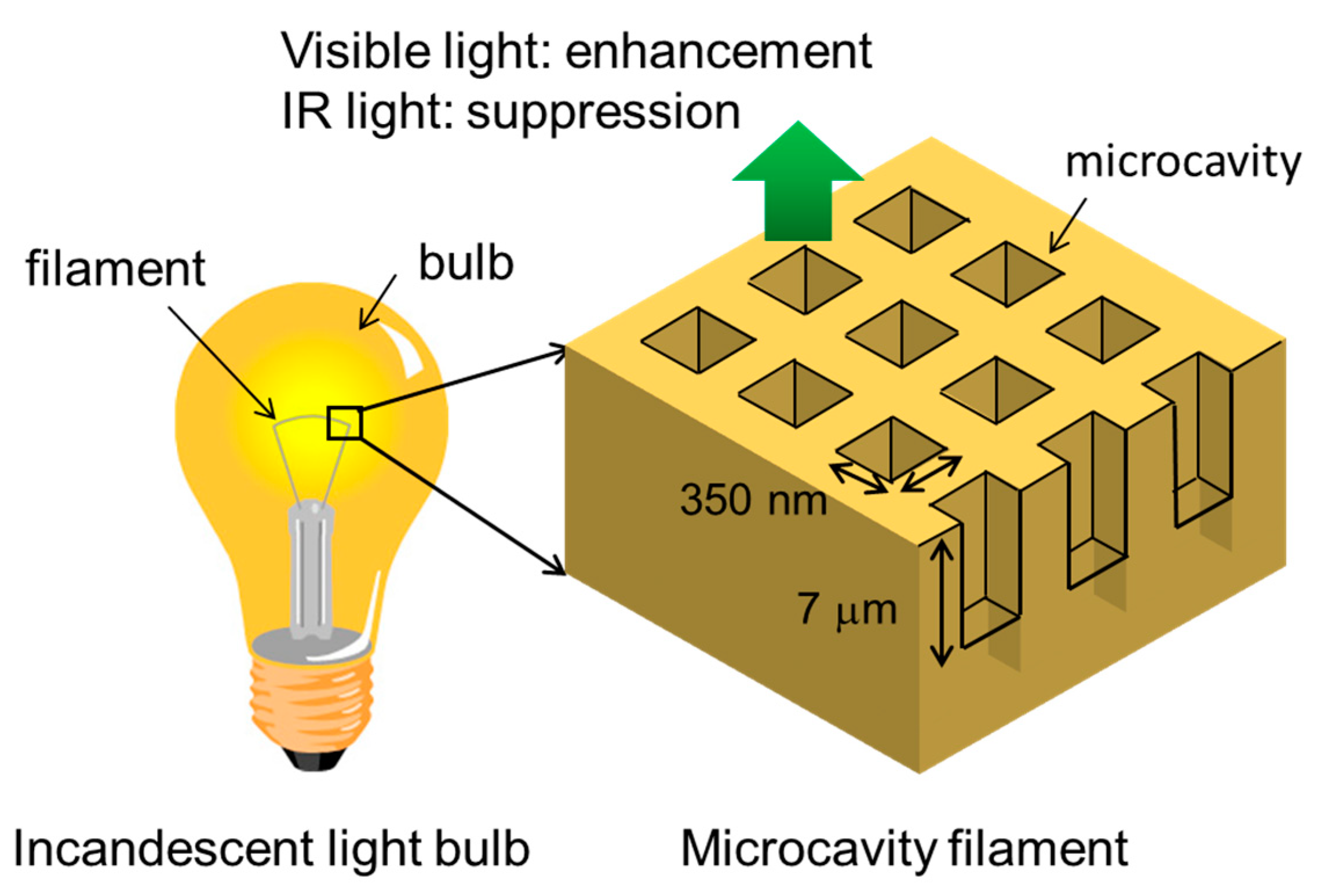
1. Introduction
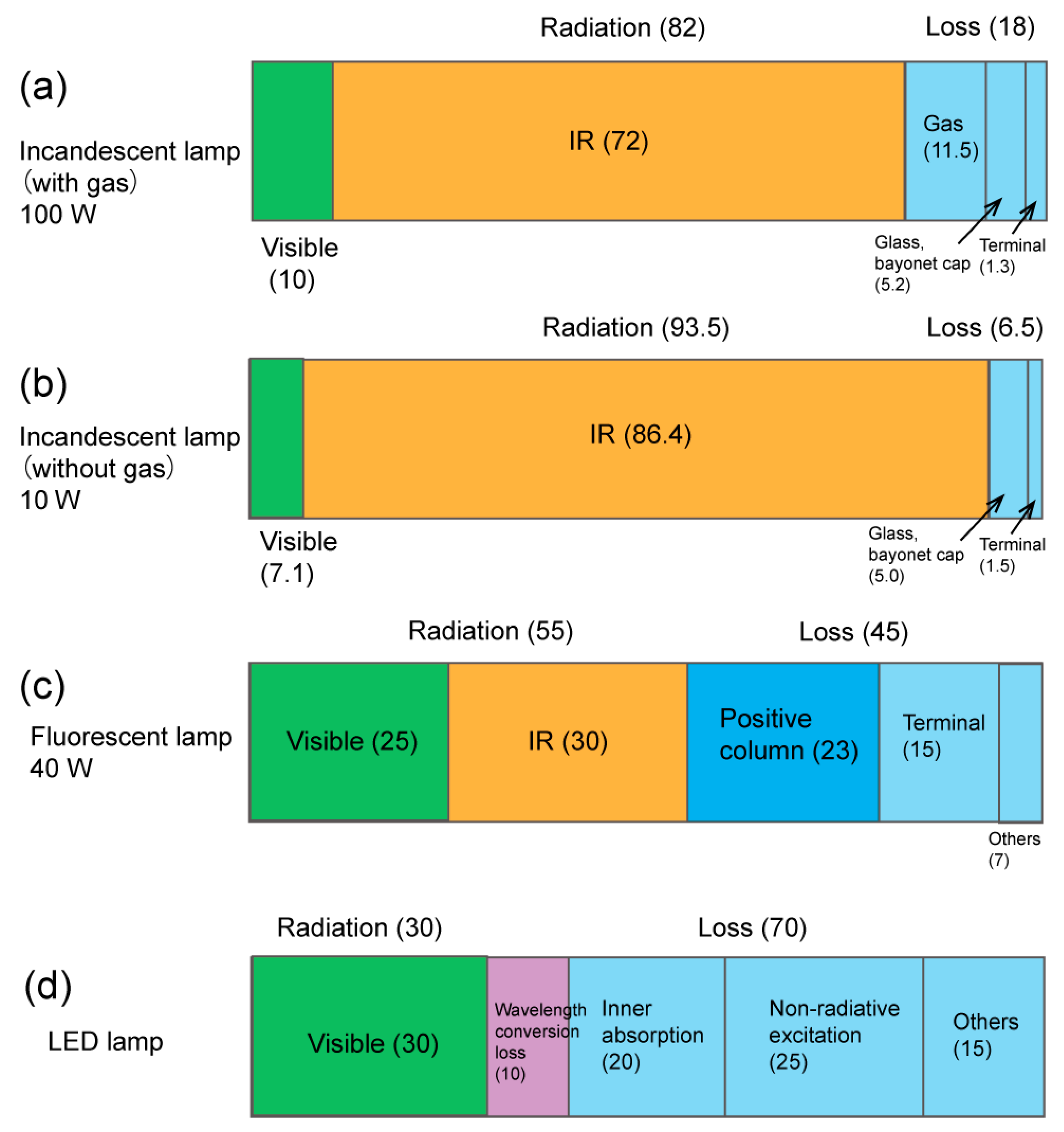
2. The Efficiency of Thermal Radiation Light Sources
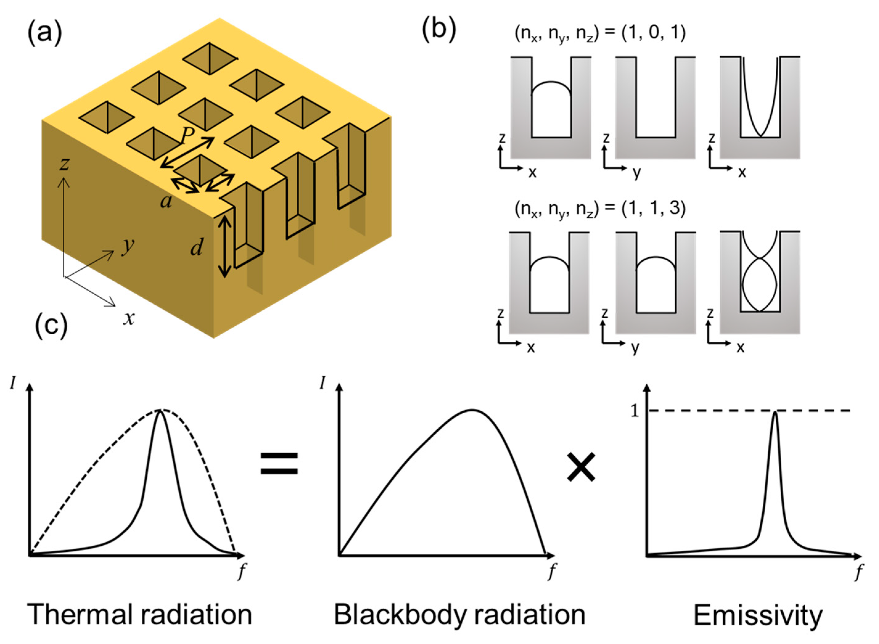
3. The Basic Principle of Thermal Radiation Control by a Refractory Metasurface
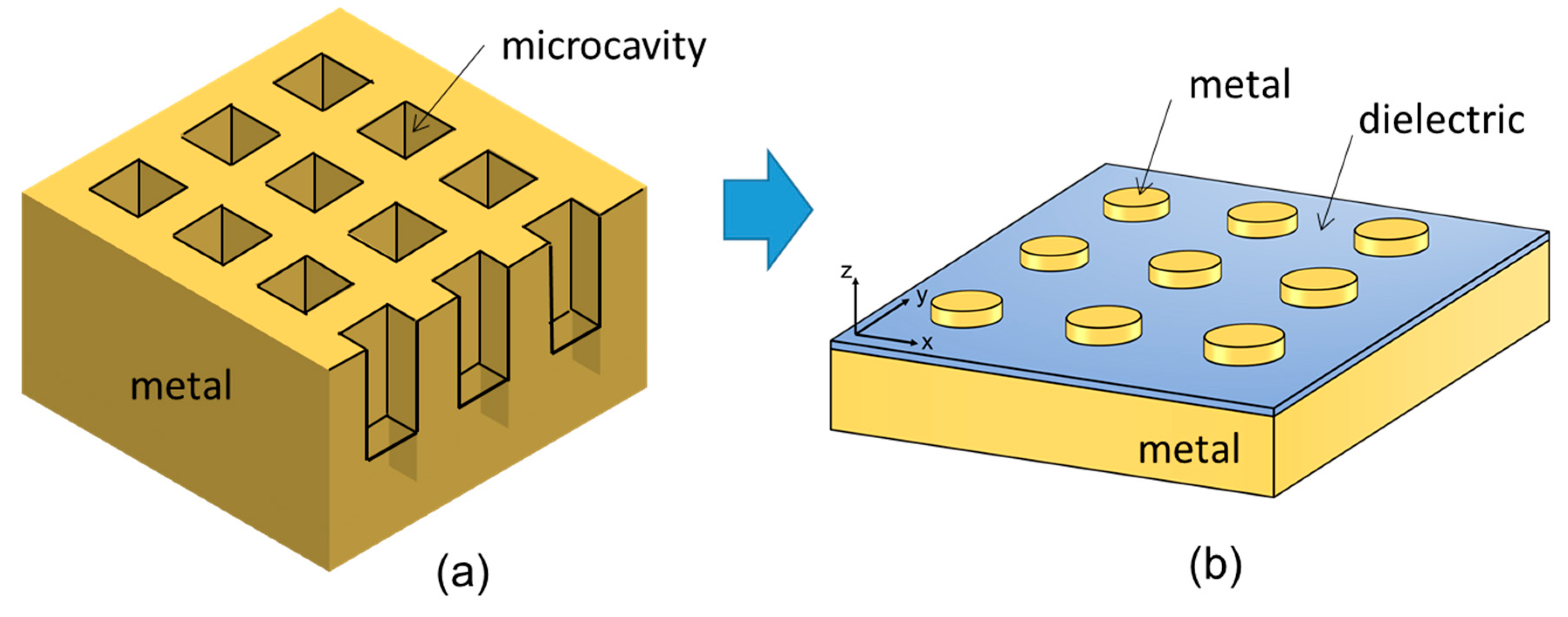
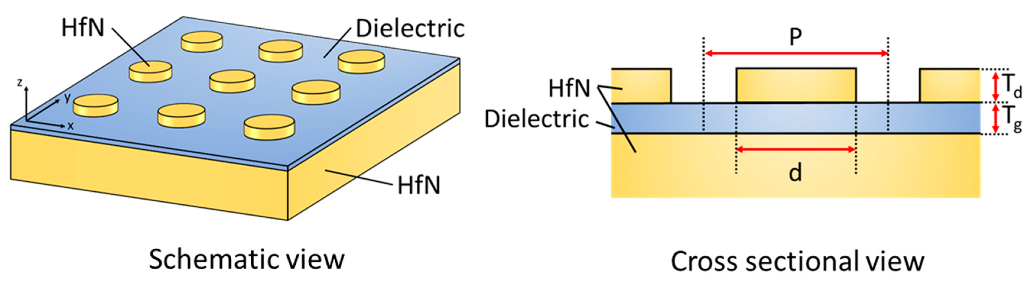
4. Thermal Radiation Control by a Microcavity Array
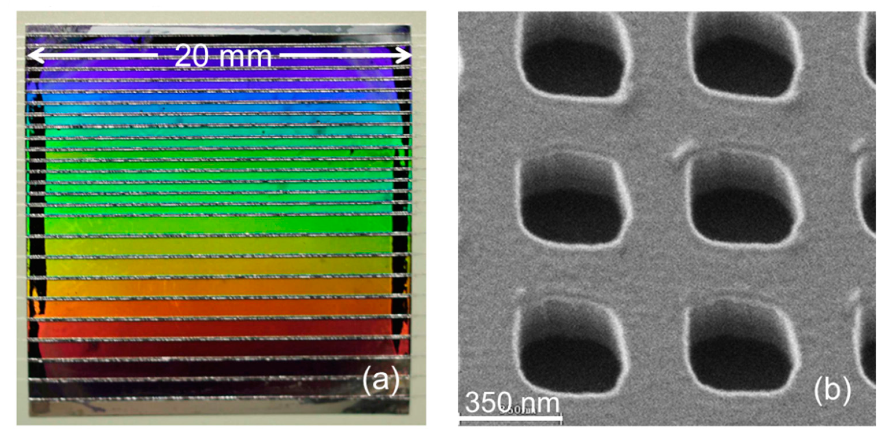
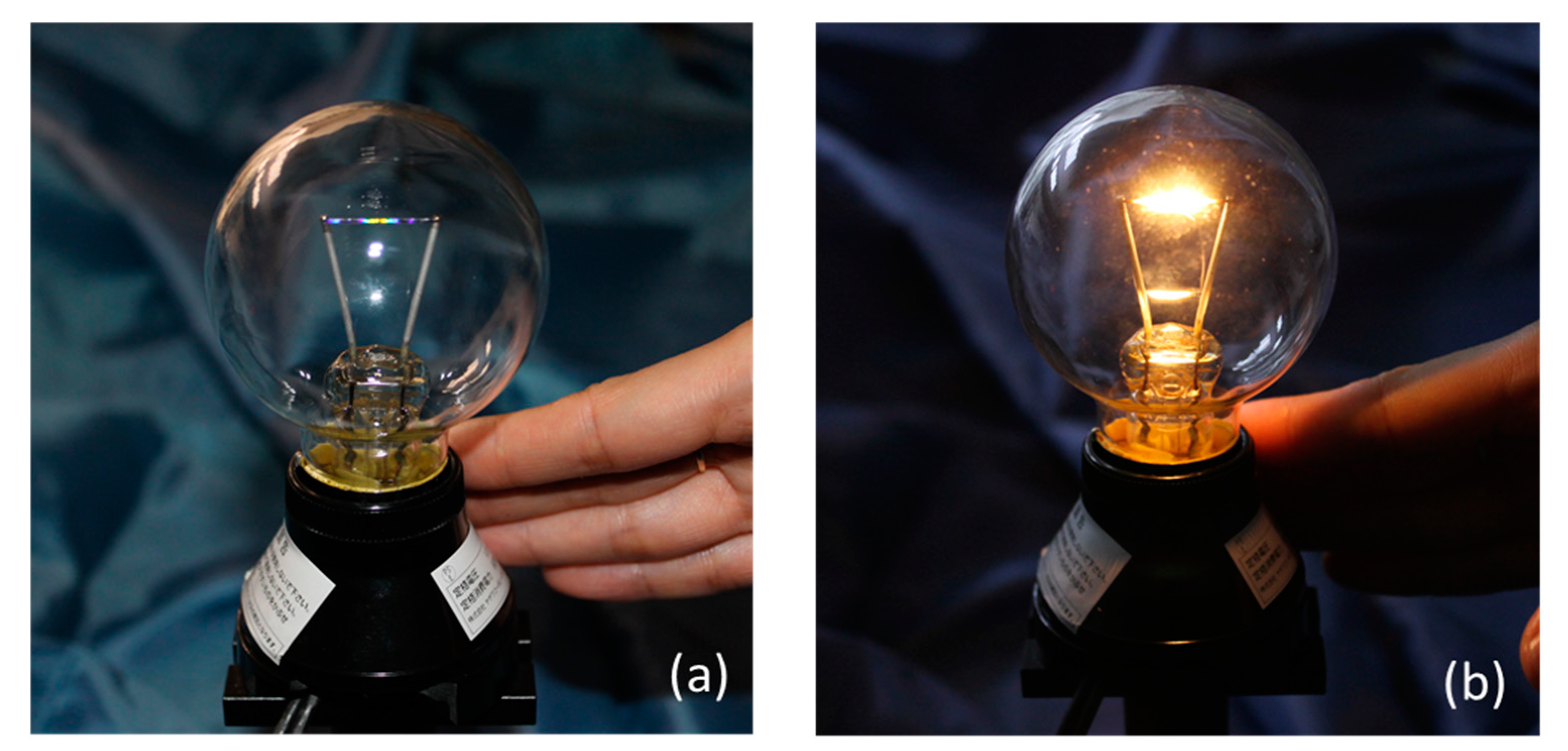
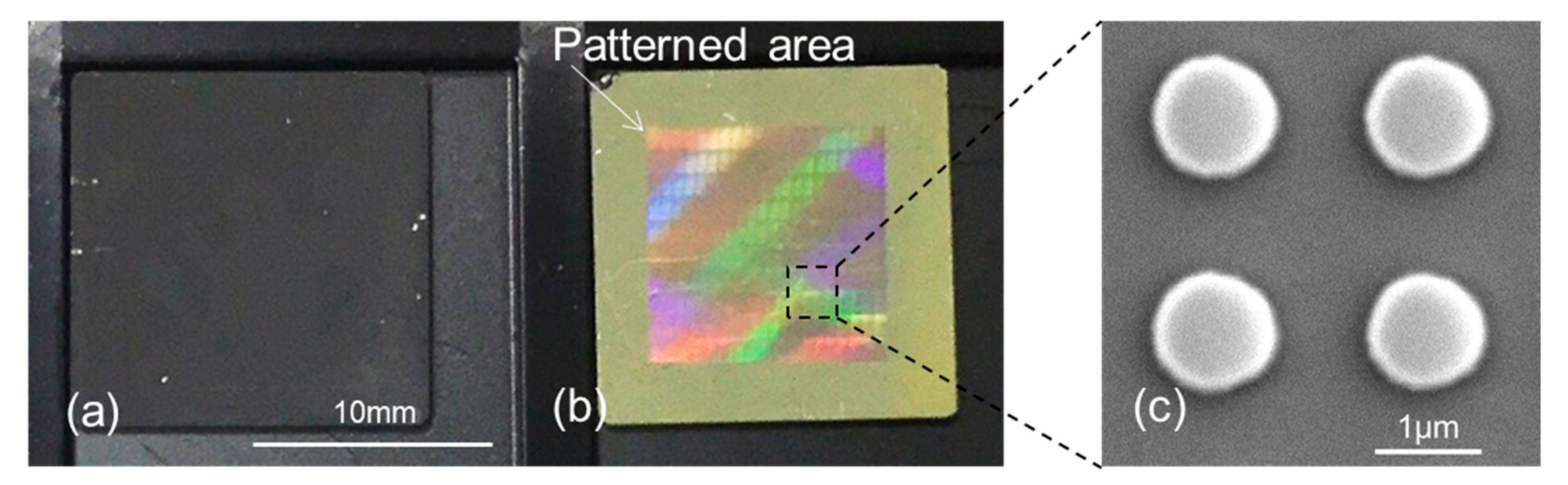
4.1. Fabrication by Nanoimprint
4.2. Measurements
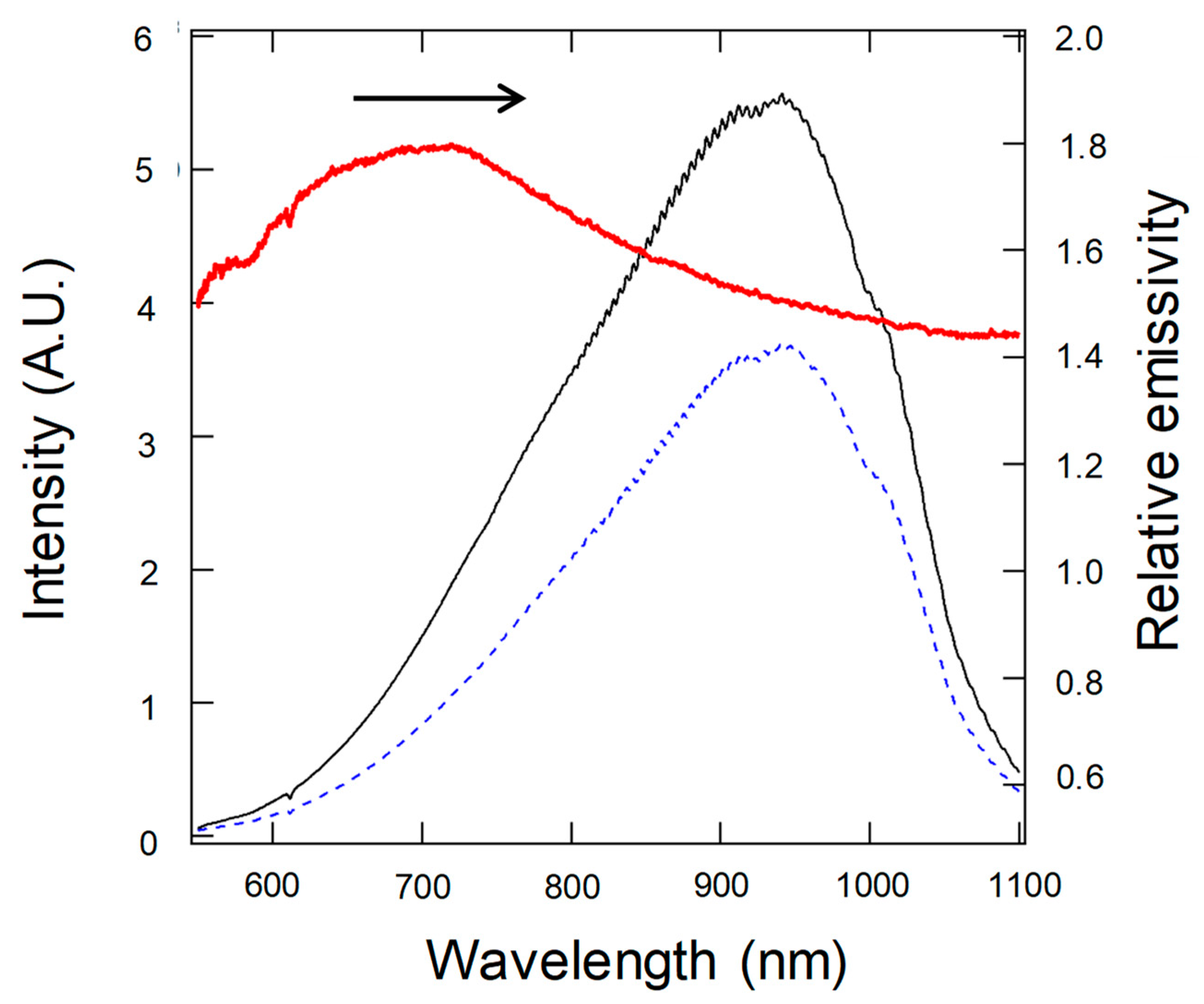
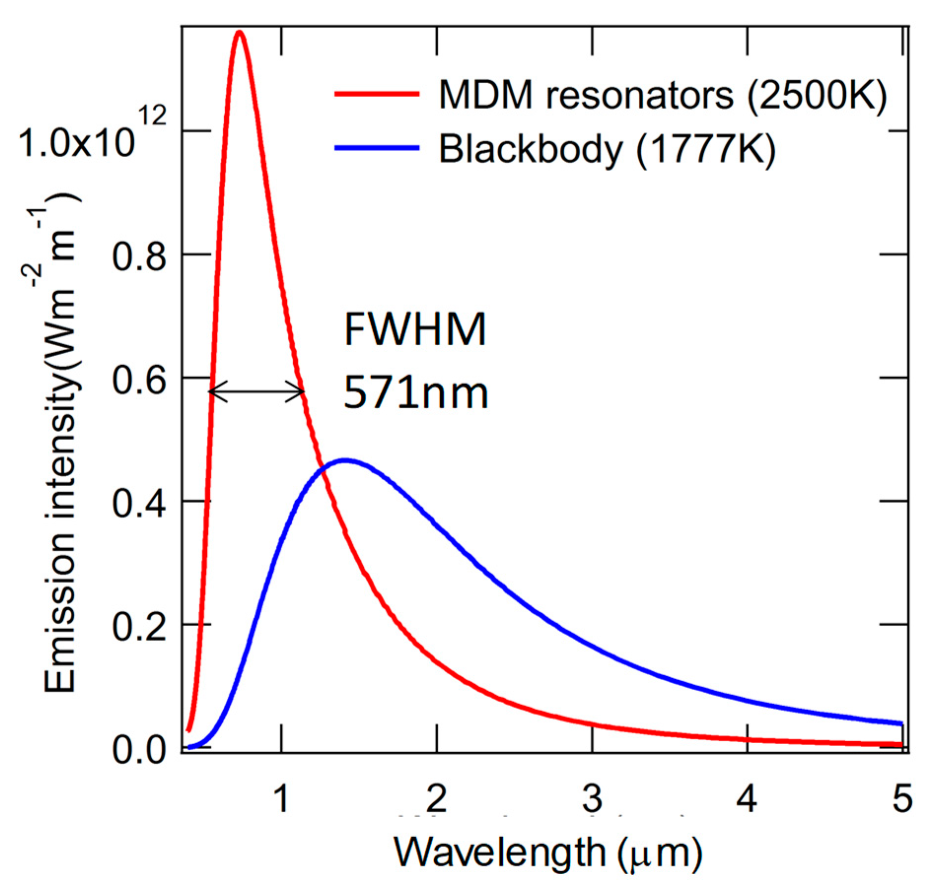
4.3. Results and Discussion
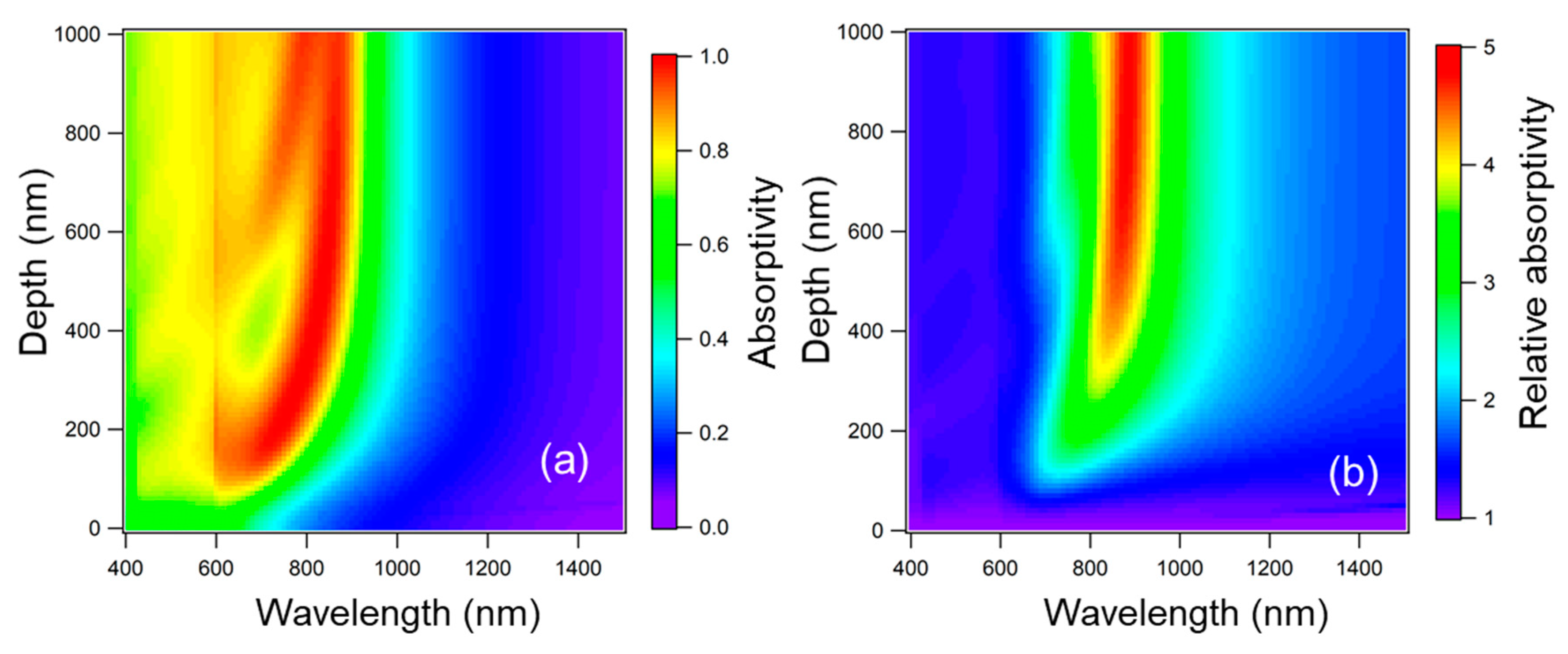
4.4. Simulated Results
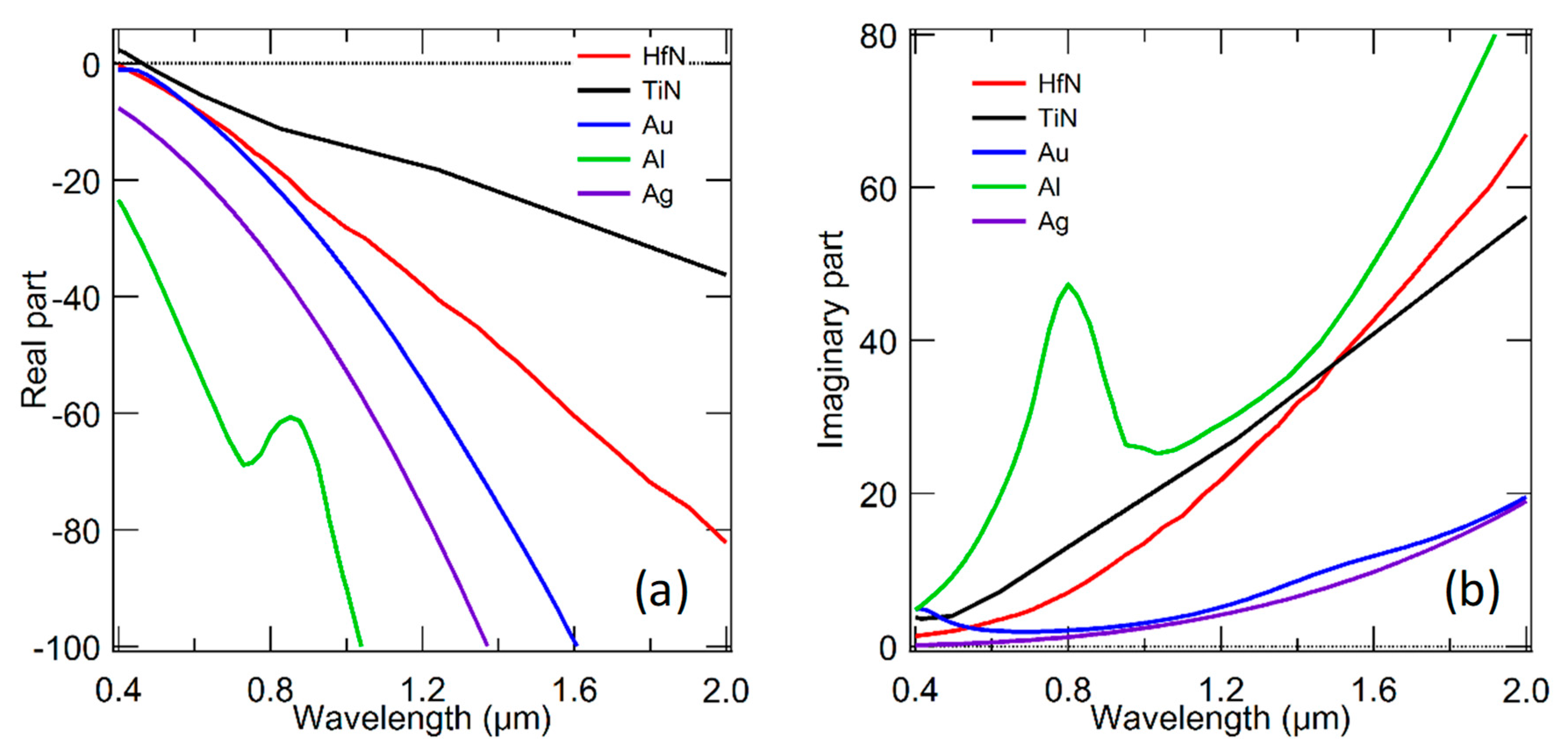
5. Thermal Radiation Control by a Refractory Plasmonic Metasurface
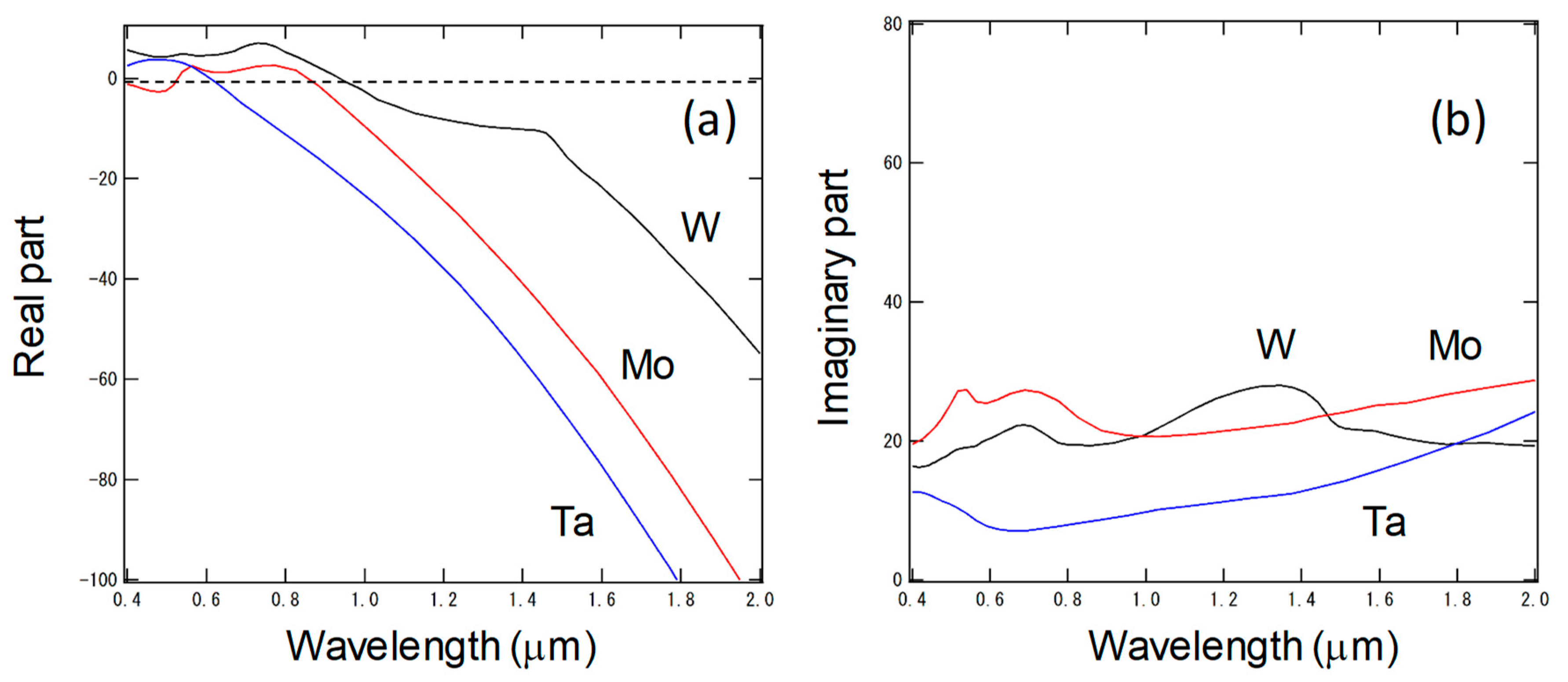
5.1. Thermal Radiation Control by Plasmonic Cavities
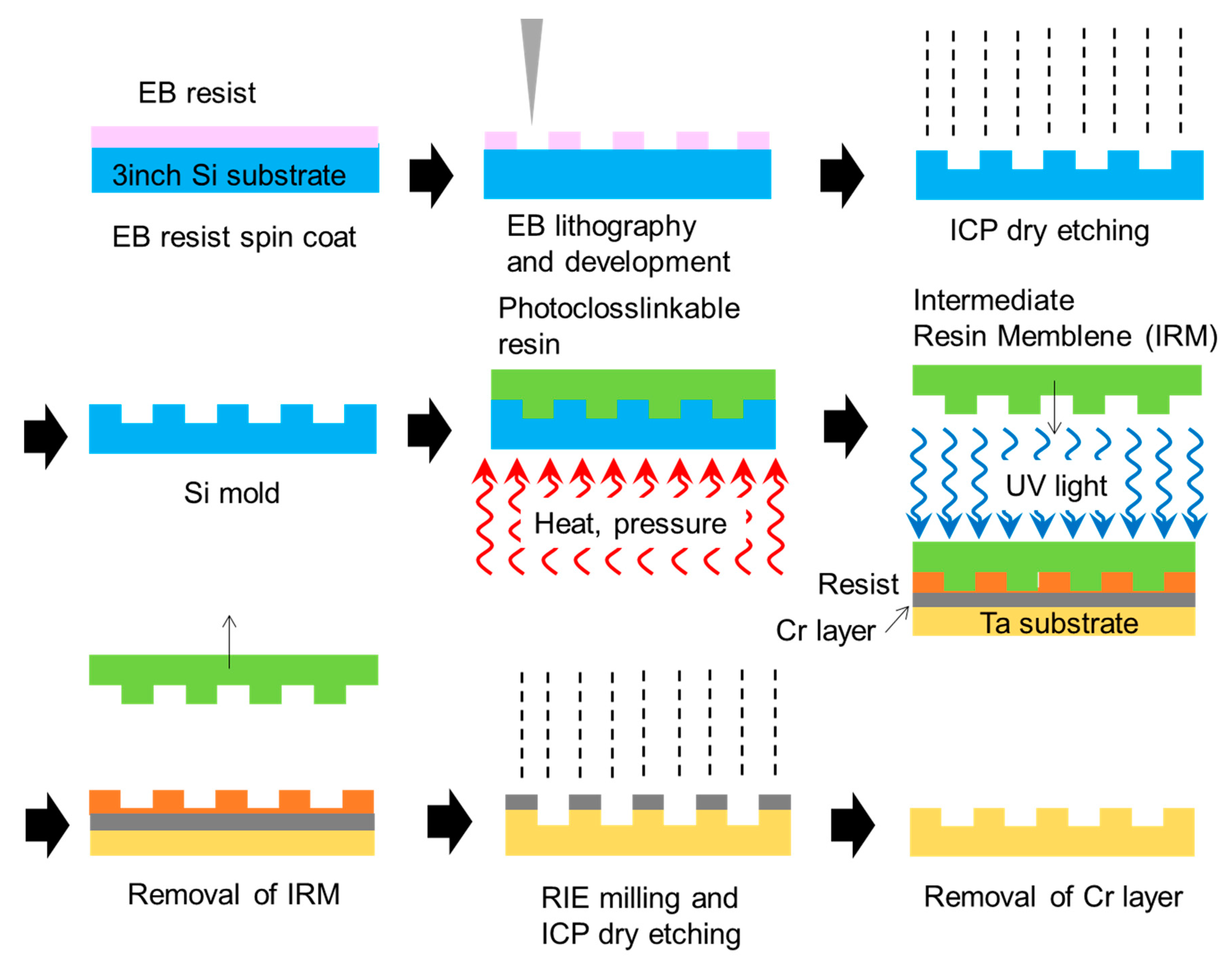
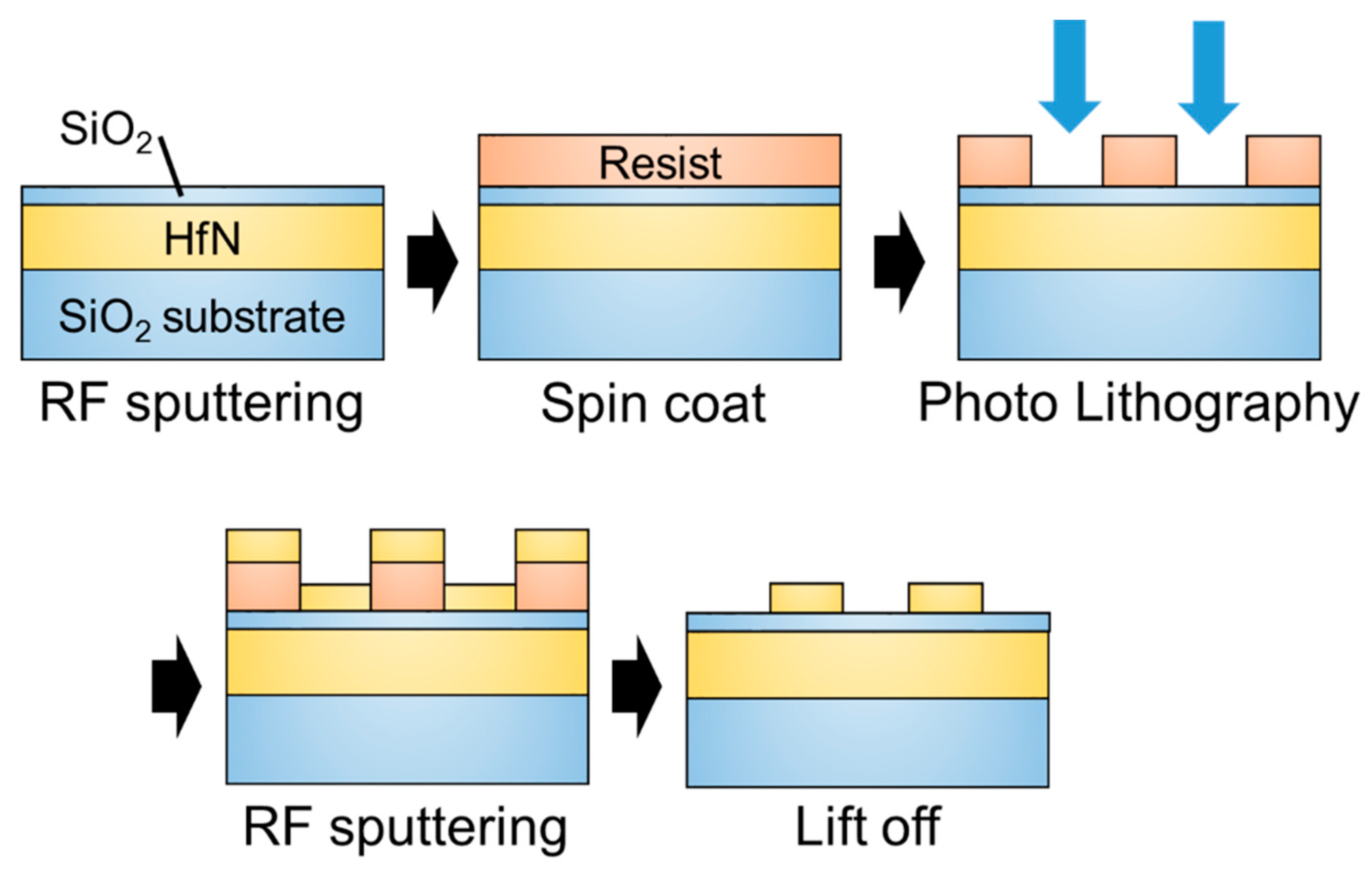
5.2. Fabrication
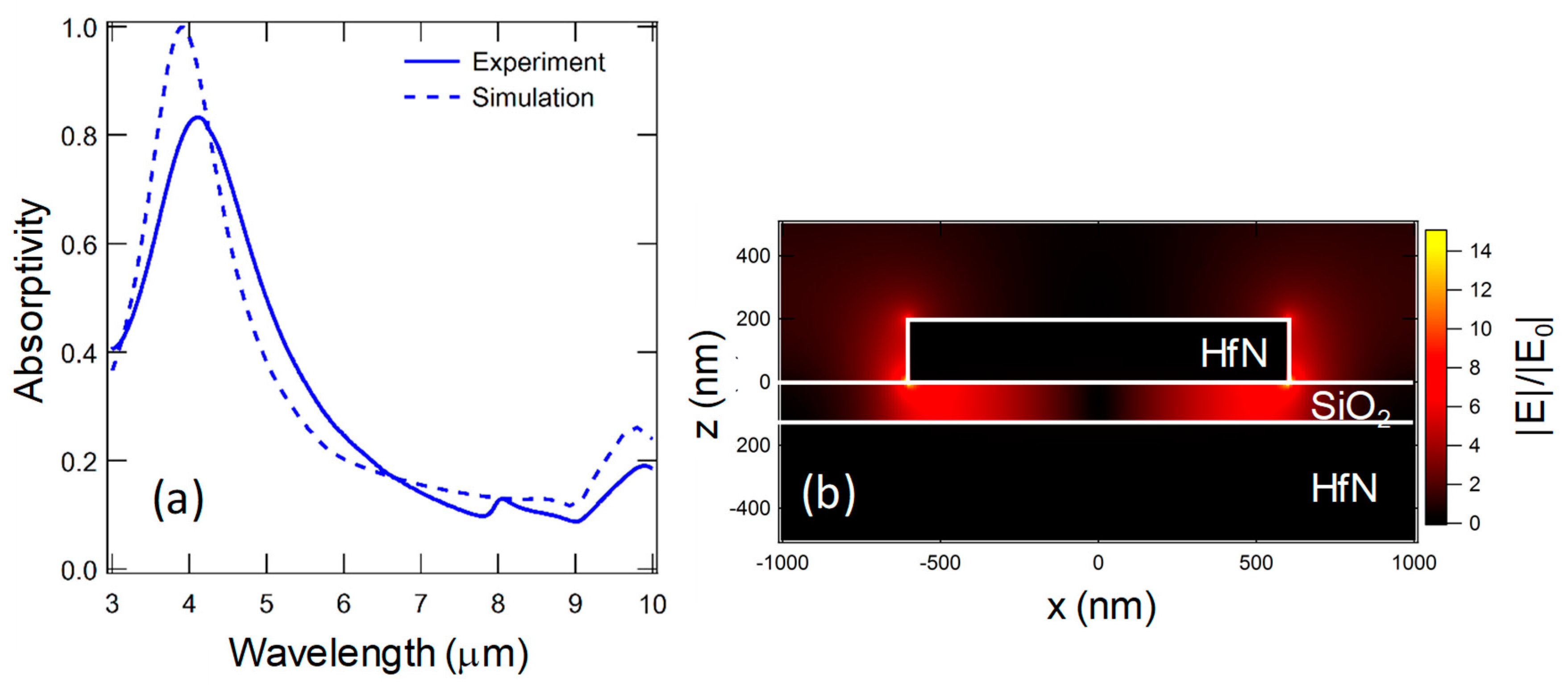
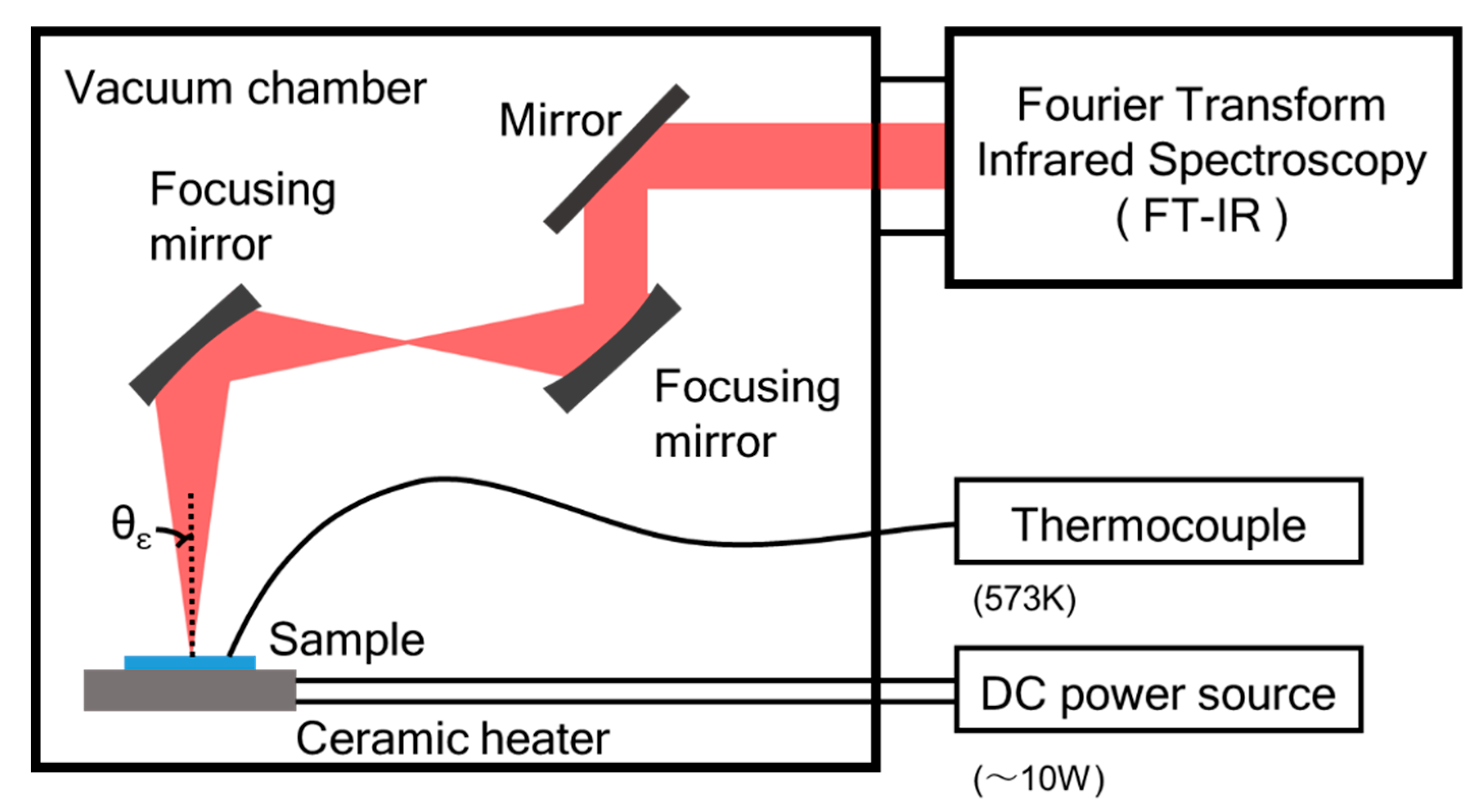
5.3. Measurements
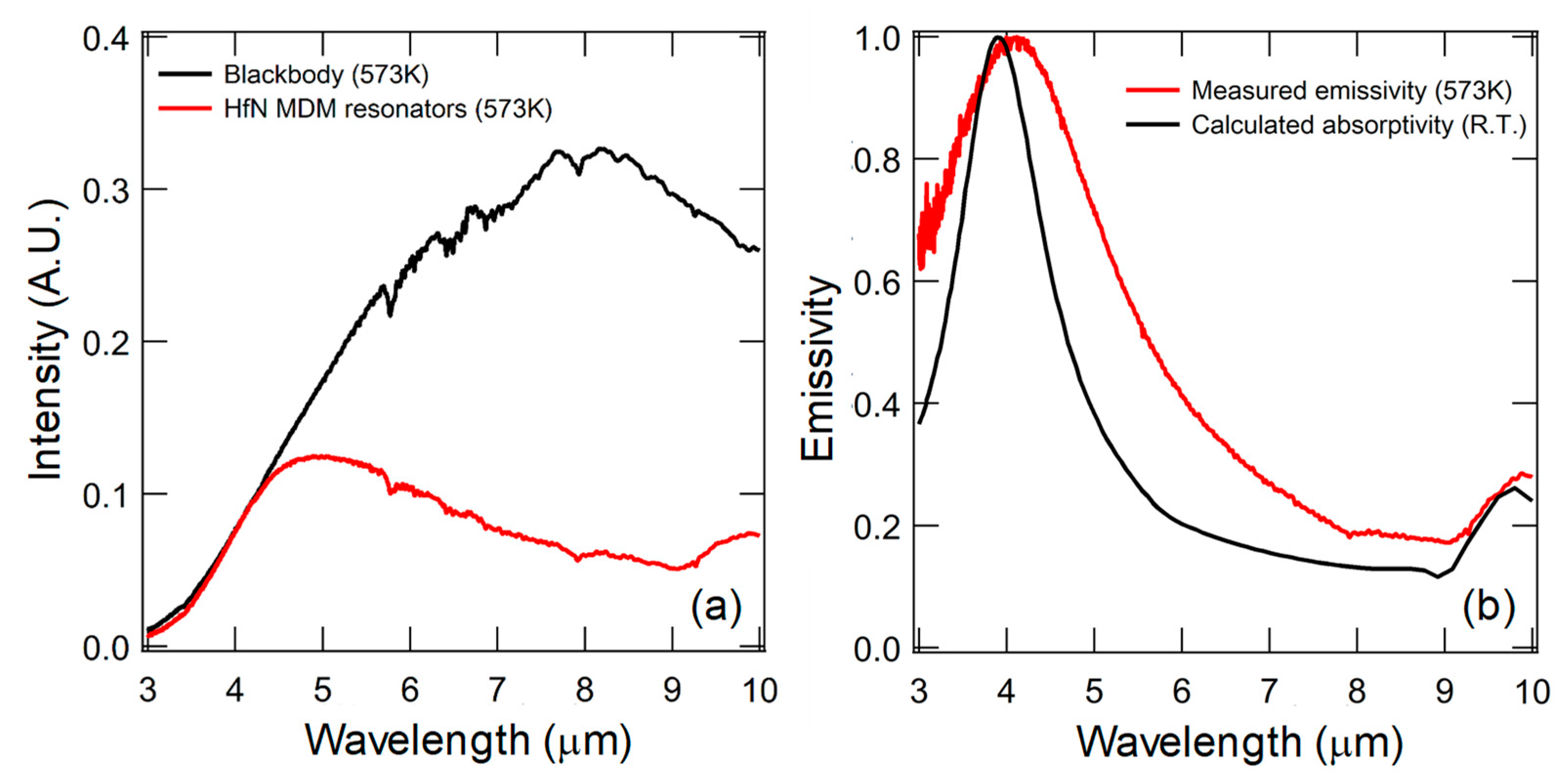
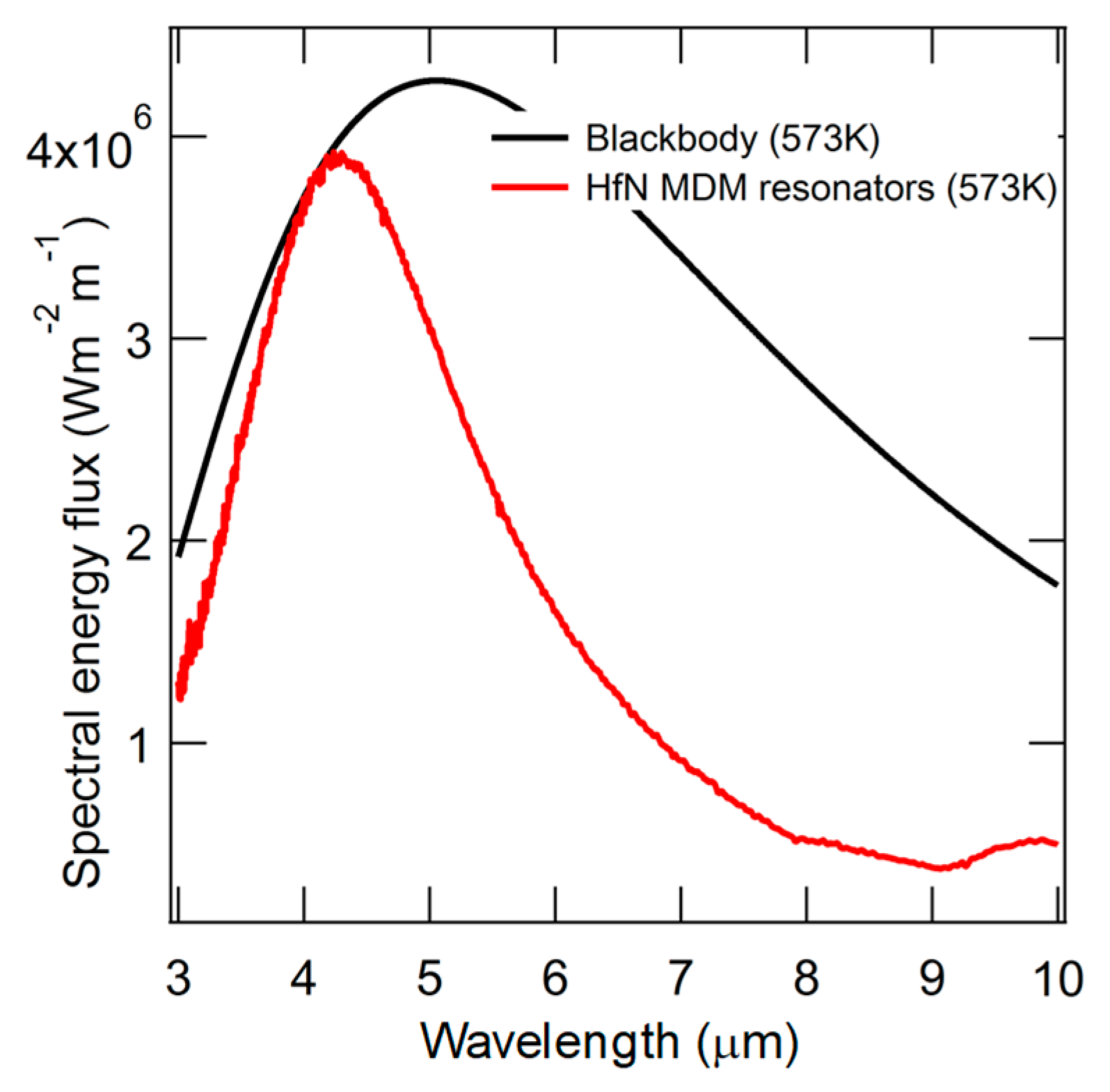
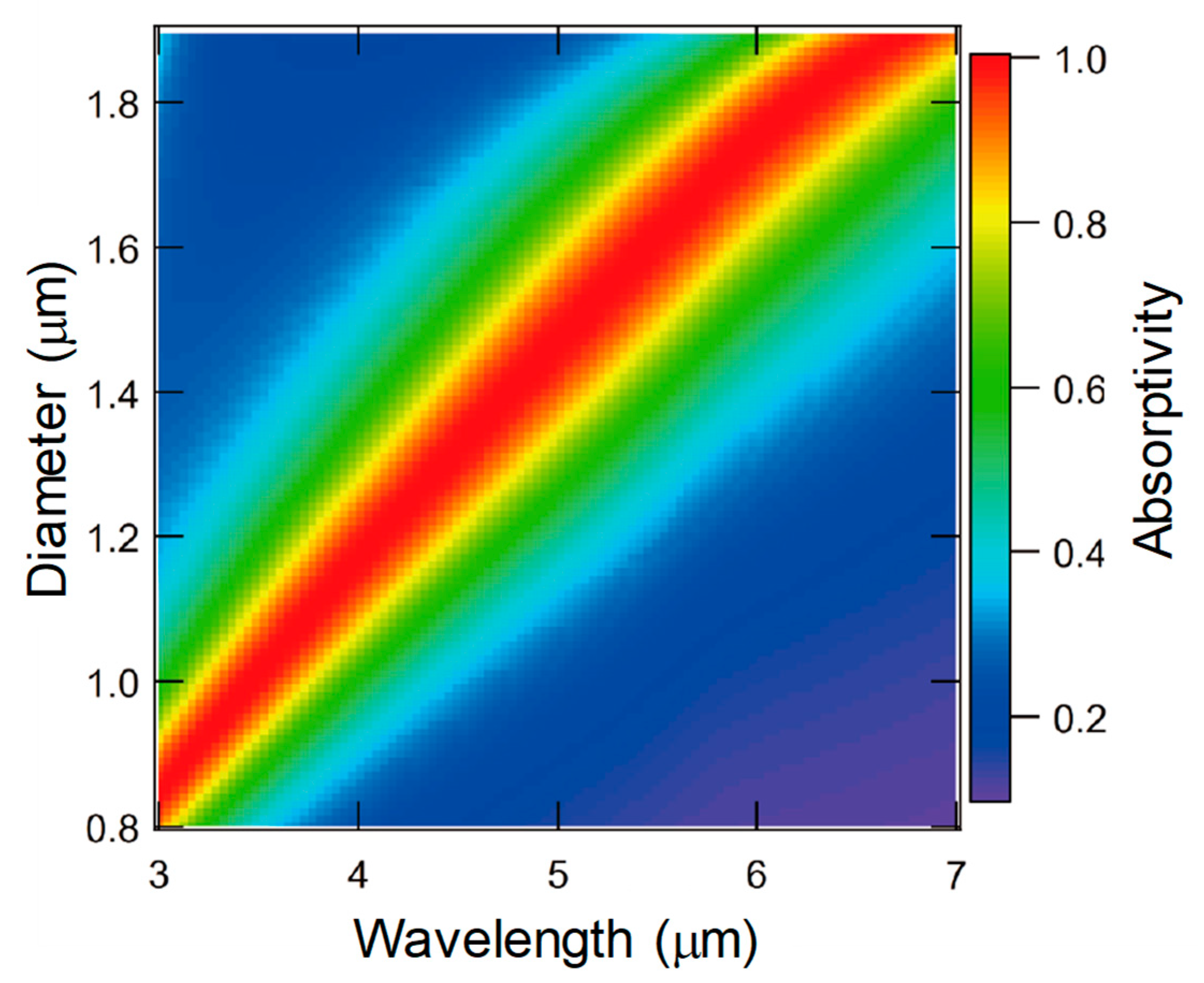
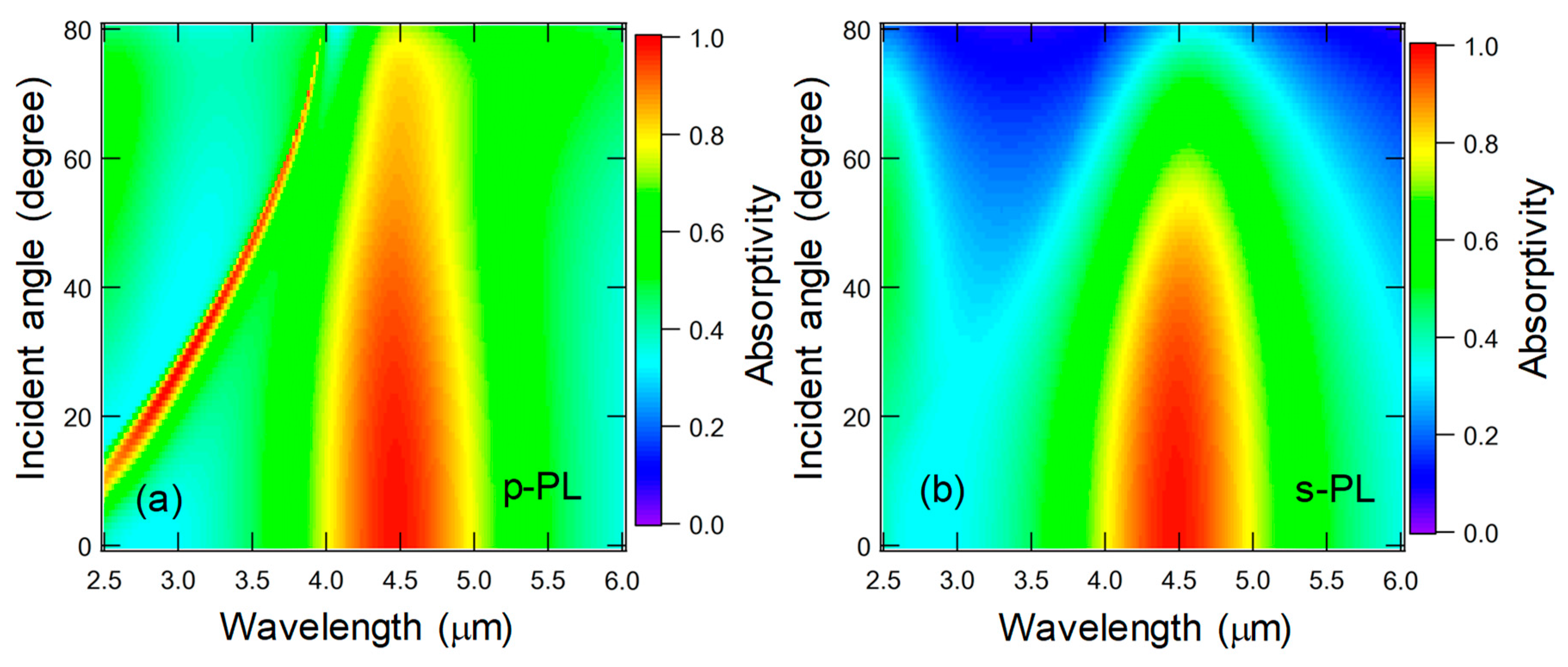
5.4. Results and Discussion
6. Conclusions
Author Contributions
Funding
Acknowledgments
Conflicts of Interest
Appendix A

Appendix B

Appendix C

Appendix D

Appendix E

Appendix F

Appendix G

References
- Takahara, J.; Ueba, Y.; Nagatsuma, T. Thermal radiation control by microcavity and ecological incandescent lamps. Jpn. J. Opt. 2010, 39, 482–488. [Google Scholar]
- Takahara, J.; Ueba, Y. Thermal Infrared Emitters by Plasmonic Metasurface. Proc. SPIE 2013, 8818, 88180X. [Google Scholar]
- Waymouth, J.F. Where will the next generation of lamps come from? J. Illum. Energy Inst. Jpn. 1990, 74, 800. [Google Scholar] [CrossRef]
- Waymouth, J.F. Optical Light Source Devices. U.S. Patent 5,079,473, 7 January 1992. [Google Scholar]
- Hesketh, P.J.; Zemalr, J.N.; Gebhart, B. Organ pipe radiant modes of periodic micromachined silicon surface. Nature 1986, 324, 549–551. [Google Scholar] [CrossRef] [PubMed]
- Maruyama, S.; Kashiwa, T.; Yugami, H.; Esashi, M. Thermal radiation from two-dimensionally confined modes in microcavities. Appl. Phys. Lett. 2001, 79, 1393–1395. [Google Scholar] [CrossRef]
- Kusunoki, F.; Kohama, T.; Hiroshima, T.; Fukumoto, S.; Takahara, J.; Kobayashi, T. Narrow-Band Thermal radiation with Low Directivity by Resonant Modes inside Tungsten Microcavities. Jpn. J. Appl. Phys. 2004, 43, 5253–5258. [Google Scholar] [CrossRef]
- Lin, S.Y.; Fleming, J.G.; Chow, E.; Bur, J.; Choi, K.K.; Goldberg, A. Enhancement and suppression of thermal emission by a three-dimensional photonic crystal. Phys. Rev. 2000, 62, R2243–R2246. [Google Scholar] [CrossRef]
- Zoysa, M.D.; Asano, T.; Mochizuki, K.; Oskooi, A.; Inoue, T.; Noda, S. Conversion of broadband to narrowband thermal emission through energy recycling. Nat. Photonics 2012, 6, 535–539. [Google Scholar] [CrossRef]
- Ikeda, K.; Miyazaki, H.T.; Kasaya, T.; Yamamoto, K.; Inoue, Y.; Fujimura, K.; Kanakugi, T.; Okada, M.; Hatada, K.; Kitagawa, S. Controlled thermal emission of polarized infrared waves from arrayed plasmon nanocavities. Appl. Phys. Lett. 2008, 92, 021117. [Google Scholar] [CrossRef]
- Miyazaki, H.; Ikeda, K.; Kasaya, T.; Yamamoto, K.; Inoue, Y.; Fujimura, K.; Kanakugi, T.; Okada, M.; Hatade, K.; Kitagawa, S. Thermal emission of two-color polarized infrared waves from integrated plasmon cavities. Appl. Phys. Lett. 2008, 92, 141114. [Google Scholar] [CrossRef]
- Schuller, J.A.; Taubner, T.; Brongersma, M.L. Optical antenna thermal emitters. Nat. Photonics 2009, 3, 658–661. [Google Scholar] [CrossRef]
- Greffet, J.J.; Carminati, R.; Joulain, K.; Mulet, J.P.; Mainguy, S.; Chen, Y. Coherent emission of light by thermal sources. Nature 2002, 416, 61–62. [Google Scholar] [CrossRef] [PubMed]
- Kusunoki, F.J.; Kobayashi, T. Qualitative change of resonant peaks in thermal emission from periodic array of microcavities. Electron. Lett. 2003, 39, 23–24. [Google Scholar] [CrossRef]
- Biener, G.; Dahan, N.; Niv, A.; Kleiner, V.; Hasmana, E. Highly coherent thermal emission obtained by plasmonic bandgap structures. Appl. Phys. Lett. 2008, 92, 081913. [Google Scholar] [CrossRef]
- Ueba, Y.; Takahara, J.; Nagatsuma, T. Thermal radiation control in the terahertz region using the spoof surface plasmon mode. Opt. Lett. 2011, 36, 909–911. [Google Scholar] [CrossRef]
- Yang, Z.Y.; Ishii, S.; Yokoyama, T.; Dao, T.D.; Sun, M.-G.; Nagao, T.; Chen, K.-P. Tamm plasmon selective thermal emitters. Opt. Lett. 2016, 41, 4453–4456. [Google Scholar] [CrossRef]
- Landy, N.I.; Sajuyigbe, S.; Mock, J.J.; Smith, D.R.; Padilla, W.J. Perfect Metamaterial Absorber. Phys. Rev. Lett. 2008, 100, 207402. [Google Scholar] [CrossRef]
- Watts, C.M.; Liu, X.; Padilla, W.J. Metamaterial Electromagnetic Wave Absorbers. Adv. Mater. 2012, 24, OP98. [Google Scholar] [CrossRef]
- Lee, B.J.; Wang, L.P.; Zhang, Z.M. Coherent thermal emission by excitation of magnetic polaritons between periodic strips and a metallic film. Opt. Express 2008, 16, 11328–11336. [Google Scholar] [CrossRef]
- Puscau, I.; Schaich, W.L. Narrow-band, tunable infrared emission from arrays of microstrip patches. Appl. Phys. Lett. 2008, 92, 233102. [Google Scholar] [CrossRef]
- Liu, X.; Starr, T.; Starr, A.F.; Padilla, W.J. Infrared Spatial and Frequency Selective Metamaterial with Near-Unity Absorbance. Phys. Rev. Lett. 2010, 104, 207403. [Google Scholar] [CrossRef] [PubMed]
- Liu, X.; Tyler, T.; Starr, T.; Starr, A.F.; Jokerst, N.M.; Padilla, W.J. Taming the Blackbody with Infrared Metamaterials as Selective Thermal Emitters. Phys. Rev. Lett. 2011, 107, 045901. [Google Scholar] [CrossRef] [PubMed]
- Nielsen, M.G.; Pors, A.; Albrektsen, O.; Bozhevolnyi, S.I. Efficient absorption of visible radiation by gap plasmon resonators. Opt. Express 2012, 20, 13311–13319. [Google Scholar] [CrossRef] [PubMed]
- Ueba, Y.; Takahara, J. Spectral control of thermal radiation by metasurface with a sprit-ring resonator. Appl. Phys. Express 2012, 5, 122001–122003. [Google Scholar] [CrossRef]
- Ito, K.; Toshiyoshi, H.; Iizuka, H. Densely-tiled metal-insulator-metal metamaterial resonators with quasi-monochromatic thermal emission. Opt. Express 2016, 24, 12803–12811. [Google Scholar] [CrossRef]
- Yokoyama, T.; Dao, T.D.; Chen, K.; Ishii, S.; Sugavaneshwar, R.P.; Kitajima, M.; Nagao, T. Spectrally Selective Mid-Infrared Thermal Emission from Molybdenum Plasmonic Metamaterial Operated up to 1000 °C. Adv. Opt. Mat. 2016, 4, 1987. [Google Scholar] [CrossRef]
- Miyazaki, H.T.; Kasaya, T.; Iwanaga, M.; Choi, B.; Sugimoto, Y.; Sakoda, K. Dual-band infrared metasurface thermal emitter for CO2 sensing. Appl. Phys. Lett. 2014, 105, 121107. [Google Scholar] [CrossRef]
- Matsuno, Y.; Sakurai, A. Perfect infrared absorber and emitter based on a large-area metasurface. Opt. Mat. Express 2017, 7, 618–626. [Google Scholar] [CrossRef]
- Ogawa, S.; Kimata, M. Metal-Insulator-Metal-Based Plasmonic Metamaterial Absorbers at Visible and Infrared Wavelengths: A Review. Materials 2018, 11, 458. [Google Scholar] [CrossRef]
- Baranov, D.G.; Xiao, Y.; Nechepurenko, I.A.; Krasnok, A.; Alù, A.; Kats, M.A. Nanophotonic engineering of far-field thermal emitters. Nat. Mater. 2019, 18, 920–930. [Google Scholar] [CrossRef]
- Sai, H.; Kanamori, Y.; Yugami, H. High-temperature resistive surface grating for spectral control of thermal radiation. Appl. Phys. Lett. 2003, 82, 1685–1687. [Google Scholar] [CrossRef]
- Takahara, J. Renaissance of incandescent light bulbs through nanotechnology. Oyo Buturi 2015, 84, 564–567. [Google Scholar]
- Takahara, J.; Kimino, K. Visible Spectral Control of Incandescent Light Bulbs by Microcavity Filament. In Proceedings of the Abstracts of 15th International Symposium on the Science and Technology of Lighting (LS15), Kyoto, Japan, 22–27 May 2016. 23P-LL1. [Google Scholar]
- Ilic, O.; Bermel, P.; Chen, G.; Joannopoulos, J.D.; Celanovic, I.; Soljačić, M. Tailoring high-temperature radiation and the resurrection of the incandescent source. Nat. Nanotech. 2016, 11, 320–324. [Google Scholar] [CrossRef] [PubMed]
- Shimogaki, K.; Iwai, I.; Yoshiike, H. The Luminous Efficacy of an Incandescent Lamp Which has an Infrared Reflective Film. J. Illum. Eng. Inst. Jpn. 1984, 68, 72–76. [Google Scholar] [CrossRef]
- The Illuminating Engineering Institute of Japan (IEI-J). Lighting Handbook (Compact Version); Ohmsha: Tokyo, Japan, 2006; Volume 3 2-1-2. [Google Scholar]
- IEI-J. Lighting Databook (New Edition); Ohmsha: Tokyo, Japan, 1968; Volume 3-1-2. [Google Scholar]
- IEI-J. Lighting Handbook (Compact Version); Ohmsha: Tokyo, Japan, 2006; Volume 3 2-2-2. [Google Scholar]
- IEI-J. 34th Textbook of Lighting Basic Course (New Edition); IEI-J: Tokyo, Japan, 2013; pp. 2–23. [Google Scholar]
- Palik, E.D. Handbook of Optical Constants of Solids; Academic Press: San Diego, CA, USA, 1985. [Google Scholar]
- Boltasseva, A.; Atwater, H.A. Low-Loss Plasmonic Materials. Science 2011, 331, 290–291. [Google Scholar] [CrossRef]
- Naik, G.V.; Shalaev, V.M.; Boltasseva, A. Alternative Plasmonic Materials: Beyond Gold and Silver. Adv. Mater. 2013, 25, 3264–3294. [Google Scholar] [CrossRef]
- Guler, U.; Boltasseva, A.; Shalaev, V.M. Refractory Plasmonics. Science 2014, 344, 263–264. [Google Scholar] [CrossRef]
- Kumar, M.; Umezawa, N.; Ishii, S.; Nagao, T. Examining the Performance of Refractory Conductive Ceramics as Plasmonic Materials: A Theoretical Approach. ACS Photonics 2015, 3, 43–50. [Google Scholar] [CrossRef]


| Material | Melting Point (K) | Permittivity in Visible Range |
|---|---|---|
| Ag | 1235 | ND |
| Au | 1337 | ND |
| SiO2 | 1983 | D |
| Mo | 2896 | D |
| HfO2 | 3031 | D |
| TiN | 3203 | ND |
| Ta | 3290 | D/ND |
| HfN | 3607 | ND |
| W | 3695 | D |
© 2019 by the authors. Licensee MDPI, Basel, Switzerland. This article is an open access article distributed under the terms and conditions of the Creative Commons Attribution (CC BY) license (http://creativecommons.org/licenses/by/4.0/).
Share and Cite
Toyoda, H.; Kimino, K.; Kawano, A.; Takahara, J. Incandescent Light Bulbs Based on a Refractory Metasurface. Photonics 2019, 6, 105. https://doi.org/10.3390/photonics6040105
Toyoda H, Kimino K, Kawano A, Takahara J. Incandescent Light Bulbs Based on a Refractory Metasurface. Photonics. 2019; 6(4):105. https://doi.org/10.3390/photonics6040105
Chicago/Turabian StyleToyoda, Hirofumi, Kazunari Kimino, Akihiro Kawano, and Junichi Takahara. 2019. "Incandescent Light Bulbs Based on a Refractory Metasurface" Photonics 6, no. 4: 105. https://doi.org/10.3390/photonics6040105
APA StyleToyoda, H., Kimino, K., Kawano, A., & Takahara, J. (2019). Incandescent Light Bulbs Based on a Refractory Metasurface. Photonics, 6(4), 105. https://doi.org/10.3390/photonics6040105