Article

An Optical Power Divider Based on Mode Coupling Using GaN/Al2O3 for Underwater Communication

by
Retno Wigajatri Purnamaningsih
1,*,
Nji Raden Poespawati
1,
Tomy Abuzairi
1 and
Elhadj Dogheche
2
1
Department of Electrical Engineering, Faculty of Engineering, Universitas Indonesia, Depok 16424, Indonesia
2
Université Polytechnique Hauts de France, CNRS IEMN DOAE, 59300 Valenciennes, France
*
Author to whom correspondence should be addressed.
This paper is an extended version of our paper: A GaN/sapphire 1 × 4 Optical Power Splitter Using Five Rectangular Waveguide for Underwater Application. Purnamaningsih, R.W.; Hamidah, M.; Fithriaty, D.; Gumelar, M.R.; Poespawati, N.R.; Dogheche, E. In Proceeding of 2018 IEEE 5th International Conference on Engineering Technologies and Applied Sciences (ICETAS), Bangkok, Thailand, 22–23 November 2018.
Photonics 2019, 6(2), 63; https://doi.org/10.3390/photonics6020063
Submission received: 7 April 2019 / Revised: 30 May 2019 / Accepted: 31 May 2019 / Published: 3 June 2019
(This article belongs to the Special Issue Advanced Optical Materials and Devices)

Abstract

:
This paper details the design of a 1 × 8 optical power divider, using a gallium nitride (GaN) semiconductor on sapphire, which can be applied to underwater optical wireless communication. The design consists of nine parallel rectangular waveguides which are based on mode coupling phenomena. Analysis of the design was performed using the beam propagation method (BPM). The optimization was conducted using the 3D finite difference (FD)-BPM method with an optical signal input at the wavelength required for maritime application of λ = 0.45 µm. The signal was injected into the central waveguide. The results showed that at a propagation length of 1480 µm the optical power is divided into eight output beams with an excess loss of 0.46 dB and imbalance of 0.51 dB. The proposed design can be further developed and applied in future underwater communication technology.

1. Introduction

Underwater activities, such as military activities, environmental monitoring, and oceanographic research frequently involve the deployment of unmanned or robotically operated underwater vehicles. When underwater activities are critical and time-sensitive operations, marine systems need to be equipped with ultrafast wireless communication solutions for delivering information through live video streaming [1]. These activities require high bandwidth and high capacity communication. So far, applications of single-view and multiple view video transmission are possible over an underwater acoustic path by exploiting the information perceived in the marine environment [2,3]. However, the speed of acoustic waves in salt water, i.e., approximately 1,500 m/s is significantly lower than that of light. Slow speed causes a propagation delay of a few hundred milliseconds during transmission. Such a long propagation delay affects the quality of experience in video delivery systems [4].
High bandwidth and low latency underwater optical wireless communication (UOWC) has prompted many scientists to perform research and determine the future technology of underwater communication. Recently, GaN-based laser diodes (LD) [5,6], light emitting diodes (LED) [7,8] and photodetectors have developed significantly [9,10]. These light source and detector characteristics are suitable for UOWC [11] due to the operating wavelength matching with the optical properties of seawater. Aside from the ability to emit and detect in UV-blue regions, which is suitable for the optical properties of the seawater [12], the GaN semiconductor has shown the potential to be applied in waveguide based photonic devices. Currently, the design of waveguide-based photonic devices has been extensively developed. This includes the optical power splitter [13], coupler, demultiplexer [14], and waveguide intersection [15].
Optical power splitters are one of the most elementary devices in a photonic system. Therefore their quality is significant in achieving high system performance. So far, research on optical power splitters had been proposed in various literature studies. An eight branch silicon on insulator (SOI) based multimode interference power splitter has been developed [16]. A wide wavelength range of optical power splitters with an imbalance of less than ± 1.0 dB have also been successfully developed. Recently, a four branch power splitter using photonic crystal ring resonators designed in a 2-D square lattice of dielectric rods in air background was presented [17]. The design was proposed for 1550 nm wavelength and is reported to have an overall device efficiency of 84.68%. An optical power splitter using SiN with high transmission efficiency for both TE and TM polarizations over a broad bandwidth ranging from 1400 nm to 1700 nm has been proposed. The proposed structure is ultra-compact with only 13 µm length [18]. A silicon integrated broadband and low loss optical power splitter had been developed. The power splitter based on light coupling between three parallel tapered waveguides was developed with an excess loss of < 0.1 dB over a wide wavelength range of 317 nm [19].
The III-nitride semiconductor has received considerable interest so far [20,21]. III-nitride optoelectronic devices can operate at high temperature and high power levels due to their mechanical hardness and large band offsets. Additionally, the III-nitride semiconductor has temperature stability, which ensures its suitability for a harsh environment [22].
So far, the III-nitride based photonic device design of the Y junction, and multimode interference (MMI) structure splitter, used for high-speed optical communication systems, has been demonstrated [23,24]. The design of a free-standing GaN waveguide has also been reported [25]. Photonic integration for multifunctional devices, based on this material, has been developed [26]. Recently, the design of optical power splitters for underwater communications has also been described [27,28].
In this paper, the design of a 1 × 8 optical power splitter, using nine parallel rectangular waveguides based on mode coupling phenomena is documented. The optimization was conducted using OptiBPM software and Matlab.

2. Proposed Design of the GaN-Based Optical Power Divider and Numerical Analysis

2.1. The Proposed Design of the Optical Power Splitter

The operating principles of the proposed splitter are based on mode coupling phenomena. When the two waveguides (waveguide 1 and 2) are infinitely far apart, each of these waveguide modes will propagate independently with their propagation constants β 1 and β 2 . However, when the two waveguides are close, they become coupled and exchange power as a function of propagation direction. Therefore, the spatial dependences of one mode amplitude will be modified by the other [29,30,31]. The efficiency of the power transfer from one waveguide to another waveguide due to the behavior of the supermode is represented by coupling coefficient κ . The distance over which the maximum amount of power is transferred from one waveguide to another is represented by coupling length L c defined as:
L c = λ 2 ( n s n a )
where λ is the wavelength; n s and n a are the symmetric and antisymmetric refractive indices respectively defined as following
n s =   n e f f +   κ 12
n a =   n e f f κ 21
κ 12 = κ 21 = κ
Figure 1 shows the configuration of the proposed splitter, while Figure 2 shows the structural layers of the materials within the design. In this paper, the specification of the GaN materials used for optical waveguide design was employed from the previous research [32]. The materials were grown by Metalorganic Chemical Vapor Deposition (MOCVD) on (0001) sapphire using an AlN/GaN Short Period Superlattice (SPS). Table 1 introduces all of the dimensions and the design specifications for the proposed splitter.
The proposed structure is symmetrical and identical with the input waveguide centered to the other eight rectangular output waveguides. The parameter L is the length of the input waveguide and its two adjacent waveguides. L 1 is the length of waveguides 3 and 4, L 2 is the length of waveguides 5 and 6, L 3 is the length of waveguides 7 and 8, while g is the gap between two adjacent waveguides. The main objective of the design was to obtain strong power confinement and uniform output power based on mode coupling between the adjacent waveguides. The design commenced with the optimization of the waveguide width and height, to support single mode propagation. This was followed by optimizing the gap between the adjacent waveguides, the coupling length and the length of the waveguides. The optimization was carried out for transverse electric (TE) polarization to obtain eight completely separate single modes at each output port. The Wurtzite structure of sapphire was used due to its temperature stability, which resulted in improved splitter performance. The effective refractive index of the layers used were nTE = 2.451 ± 0.001 and nTM = 2.505 ± 0.001 obtained from prism coupling measurements [32]. The numerical experiments were conducted by taken into account the losses and uniformity of the optical power distribution.
This design relies on power injection to the input waveguide. Through the application of the boundary conditions: A 1 = 1 at a propagation distance of z = 0, with the other waveguides at zero value, the power transfer from the input waveguide to the other eight waveguides can be calculated. However, due to the complexity of the structure, the numerical analysis method has to be used.

2.2. Numerical Analysis

The numerical experiment to design the proposed splitter was conducted using OptiBPM software based on a slowly varying envelope approximation combined with Matlab software. The field propagation calculation through the structure was carried out using the finite difference beam propagation method (FD-BPM). This approach was chosen since it can automatically include the calculation of all the guided and non-guided modes [33].
The derivation of the beam propagation method starts with Maxwell’s equations for electromagnetic fields in a continuous medium in the frequency domain; the electric field wave equation is written as follows:
t 2 E t + 2 E t z 2 + k 2 n 2 E t = t [ 1 n 2 ( t n 2 ) . E t ]
Using the slowly varying envelope approximation, the field transverse components E x and E y are divided into the slowly varying envelope function e t ( x , y , z ) and a spatially very fast oscillating phase term exp ( j n 0 k z ) as follows:
E t ( x , y , z ) =   e t ( x , y , z ) exp ( j n 0 k z )
where n 0 is the reference refractive index and k is the wavenumber in a vacuum.
Then, by substituting Equation (6) into Equation (5), the equation can be written as follows:
2 e t z 2 2 j k n 0 e t z + k 2 ( n 2 n 0 2 ) e t + t 2 e t + t [ 1 n 2 ( t n 2 ) . e t ] = 0
If n 0 has been set precisely, then the first term will be much smaller than the second term. Therefore, it is safe to neglect the first term. The wave equation can be rewritten into two block matrix equations as follows:
2 j k n 0 z [ e x e y ] =   [ P x x P x y P y x P y y ]
where the components of the operator P are as follows:
P x x =   x [ 1 n 2 x n 2 ] + 2 y 2 + k 2 ( n 2 n 0 2 )
P x y =   x [ 1 n 2 y n 2 ] 2 x y
P y x =   y [ 1 n 2 x n 2 ] 2 x y
P y y =   y [ 1 n 2 y n 2 ] + 2 x 2 + k 2 ( n 2 n 0 2 )
The differential operators P are approximated with finite differences, P is a large sparse matrix, and Equation (8) is applied at a given transverse plane to determine the electromagnetic field at the next transverse plane. For semi-vector TE, the equation can be simplified as:
2 j k n 0 e x z = P x x e x
The solution to the BPM equations is as follows:
e t ( z 1 ) = e x p [ Δ z P ( 2 j n 0 k ) ] e t ( z 0 )
where Δ z = z 1 z 0 . Since the field e t is assumed to be known at a transverse plane z 0 , then the above equation will calculate the field at some other plane z 1 . To solve Equation (12), the Alternating Direction Implicit (ADI) method can be employed to save computing time.

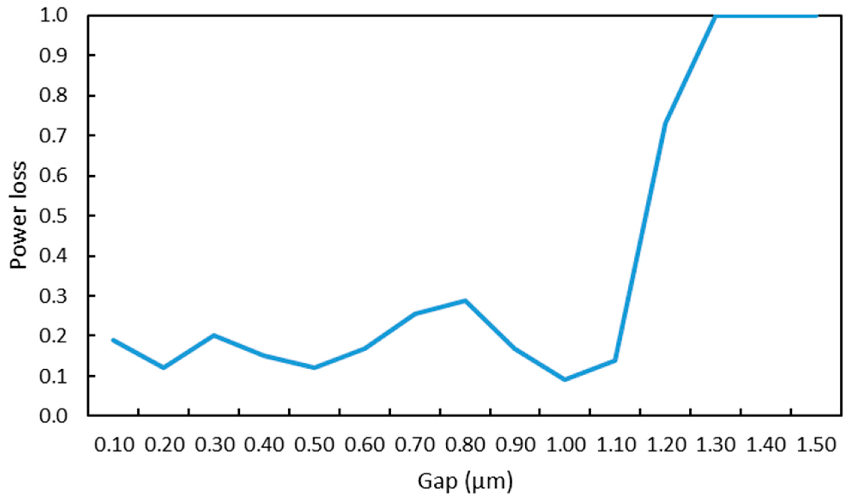
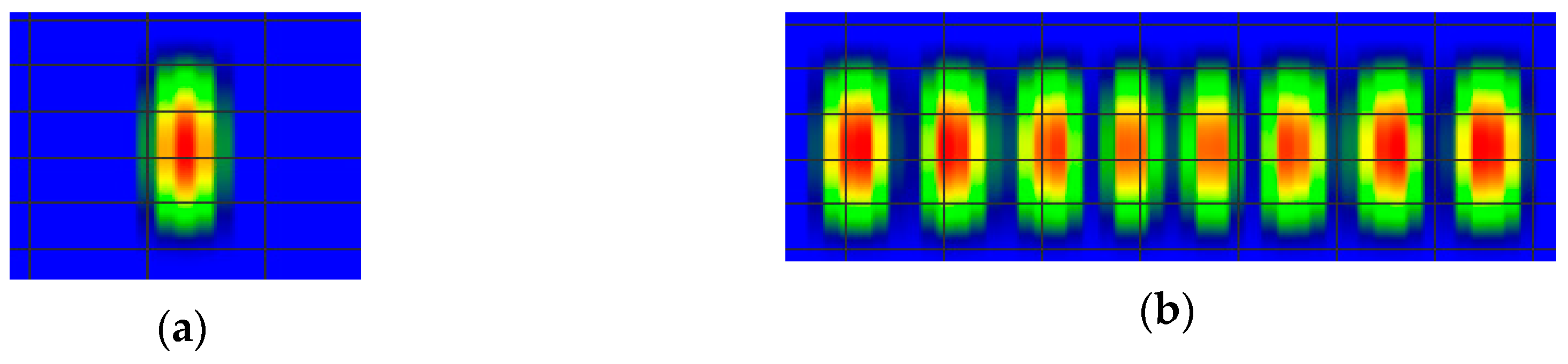
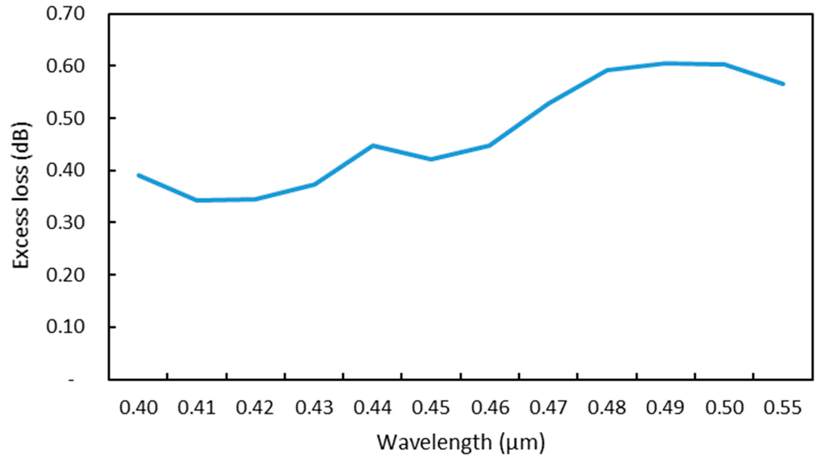
3. Simulation Results and Discussion

To obtain the best power output distribution, the parameter value of the proposed structure had to be optimized. The simulations and the numerical calculations were conducted using semi-vectorial BPM from OptiBPM combined with Matlab software. The field propagation through the structure was conducted using the finite difference beam propagation method (FD-BPM), which is suitable for the proposed design. The proposed splitter was designed using the layout designer provided in the OptiBPM which is based on the proposed mathematical model with previously mentioned design parameters. The modal input field was used as the starting field and 1 µm as the z -offset. Modal input was obtained from the Mode 3D solver calculation. After the input plane had been defined, the global data was set with the modal refractive index, and the wavelength was set at 450 nm. The proposed design performance was investigated by performing 3D isotropic simulations with a propagation step of 0.45 µm, and with the number of mesh points for both X and Y being 101. First, the width and thickness of each waveguide were varied from 2 µm up to 6.5 µm, keeping other parameters constant. The result is presented in Figure 3. It can be noted that from 2 µm up to 3 µm; 4 µm up to 5 µm, and 6 µm up to 6.5 µm the relative optical power is almost perfect at 0.999. Although the 2 µm up to 3 µm waveguide width gave the same result as the 4 µm up to 5 µm, in this work the 4 µm waveguide width was chosen.
Next, after defining the waveguide width, we optimized the optimum thickness value of each waveguide and simulation over a range from 0.5 µm up to 5 µm was carried out. The results are shown in Figure 4.
Figure 4 shows that from waveguide thickness 2 µm up to 3 µm, the relative optical power increases from 0.893 up to 0.922. From 4 µm up to 5 µm, the relative power output has an almost stable value at 0.999. Based on the results gained from the TE polarization, the optimal value for both 4 µm width and 4 µm thickness of each waveguide was chosen. This geometrical value allowed a single-mode propagation and gave the highest relative power distribution. Next, the other waveguide parameters were optimized, i.e., the gap and waveguide length. To obtain the optimum gap, the power loss was observed for various gaps between two waveguides. The gaps were varied, starting at 0.1 µm up to 1.5 µm. The results are presented in Figure 5.
Next, based on the optimum gap result, the coupling length and the coupling coefficient were calculated analytically. By solving Equation (1) combined with semi-vector BPM simulations, the value of coupling length L c and coupling length κ can be obtained. The calculated value of L c obtained was 112.323 µm with κ = 0.0140 µm−1. Then, based on this result, the length of each waveguide in the proposed structure was optimized to obtain uniform distribution and single mode propagation in each waveguide. The observation was conducted by investigated the power transfer of each waveguide, as presented in Figure 6. It can be noted that the input power completely transferred to other waveguides at z = 1480 µm.
Based on Figure 6 and the observation of the optical field profile at the output ports, it was concluded that the best length for the input waveguide was 1480 µm, the length of the output waveguides 1 and 2 were 1480 µm, waveguides 3 and 4 were 1380 µm; waveguides 5 and 6 were 1280 µm, and waveguides 7 and 9 were 1080 µm. The optimal length and width of the power splitter were found to be 1480 µm and 44 µm, respectively. These values resulted in minimal imbalance and the lowest excess loss at the operating wavelength for underwater signal transmission, λ = 0.45 µm.
Figure 7 presents the optical field distribution throughout the proposed splitter, while Figure 8 shows the mode propagation for λ = 0.45 µm at the input and output ports. It should be noted that at the input port z = 0, the optical power was a single mode, then after propagating through the proposed divider, this optical power was split into eight separate single modes. The colors red, yellow, and green in the figures represent the level of the optical field. The color red inside the GaN indicates that a strong confinement was obtained within the GaN layer.
The total relative optical power at λ = 0.45 µm throughout the propagation z -axis was also observed. The results indicate that the total relative power distribution along the proposed divider is stable at 0.99. Furthermore, the imperfection of the laser source effect on the proposed design was also investigated by examining the field pattern at the output ports using various wavelengths of the laser source, from 0.4 µm up to 0.55 µm.
Figure 9 shows the profile of the optical field at the output terminals for various wavelengths of the laser source; starting at 0.4 µm up to 0.55 µm by taking into account the dispersion obtained from previous research [32]. It should be noted that the modes were completely separated into eight single modes power output at the wavelengths of 0.44 µm, 0.45 µm, 0.49 µm, and 0.50 µm. Of the four wavelengths proven to result in eight single modes of power outputs, the wavelength of 0.45 µm gave the best optical field pattern and distribution. This indicated that the light spectrum of the laser source should be under 100 nm.
Excess loss and imbalance characterize the optical power divider. Therefore, both excess loss and imbalance calculations were also carried out. The excess loss and power imbalance of the splitter was defined as follows:
E x c e s s   L o s s =   10 l o g ( P o u t P i n )
I m b a l a n c e =   10 l o g ( P m i n P m a x )
where P o u t is the total optical output power, and P i n is the optical power injected into the input waveguide. P m i n and P m a x are the lowest and highest optical power values at the eight output ports. Based on this calculation, it was determined that the power splitter has an excess loss of 0.46 dB and yields a maximum power imbalance of 0.51 dB at λ = 0.45 µm. Furthermore, the effects of the operating wavelength variation on excess loss and imbalance were also observed, the results for the TE mode polarization are shown in Figure 10 and Figure 11.
Finally, the output power distribution of the proposed design over 100 nm spectrum scope was also investigated. The simulation was undertaken using multiple operating wavelengths between 0.4 µm and 0.5 µm using TE polarization. The results indicated that the normalized transmitted power was stable at 0.99. The guiding mechanism of the proposed design was based on mode coupling; therefore the power divider exhibits low wavelength sensitivity because it does not exhibit any interference.

4. Conclusions

A GaN/sapphire-based optical power splitter consisting of nine parallel rectangular waveguides utilizing mode coupling was studied. The previous design, which was also based on mode coupling waveguide for a 1 × 4 power splitter, was extended into a 1 × 8 optical power divider. Numerical experiments conducted, using OptiBPM FD-BPM and Matlab, showed that at the wavelength required for maritime application (of λ = 0.45 µm), the documented structure gave an excess loss of 0.46 dB with a power imbalance of 0.51 dB. Although the result was higher than the previous design [28], it is still lower than 1 dB. Since the waveguides were rectangular and symmetrical with an identical refractive index at all the waveguides, the fabrication of this proposed design splitter is easier to produce than the previously described design [23]. Therefore, the new design can be further developed for application in future underwater communication technology.

Author Contributions

Conceptualization, R.P. and E.D.; Methodology, R.P.; Software, R.P.; Validation, R.P., N.P. and T.A.; Formal Analysis, R.P.; Investigation, R.P.; Resource, R.P. and E.D.; Data Curation, R.P.; Writing—Original Draft Preparation, R.P.; Writing—Review & Editing, R.P.; Supervision, R.P. and E.D.; Project Administration, R.P.; Funding Acquisition, R.P.

Funding

This research was supported by IJR Research Grant 2018 (No:541/UN2.R3.1/HKP05.00/2018) from RISTEK DIKTI, The Republic of Indonesia.

Conflicts of Interest

The authors declare no conflict of interest. The funders had no role in the design of the study; in the collection, analyses, or interpretation of data; in the writing of the manuscript, or in the decision to publish the results.

References

  1. Kaushal, H.; Kaddoum, G. Underwater Optical Wireless Communication. IEEE Access 2016, 4, 1518–1547. [Google Scholar] [CrossRef]
  2. Zeng, Z.; Fu, S.; Zhang, H.; Dong, Y.; Cheng, J. A Survey of Underwater Optical Wireless Communications. IEEE Commun. Surveys Tuts. 2017, 19, 204–238. [Google Scholar] [CrossRef]
  3. Fujihashi, T.; Saruwatari, S.; Watanabe, T. Multiview Video Transmission Over Underwater Acoustic Path. IEEE Trans. Multimedia 2018, 20, 2166–2181. [Google Scholar]
  4. Hoeberechts, M.; Owens, D.; Riddell, D.J.; Robertson, A.D. The power of seeing: Experiences using video as a deep-sea engagement and education tool. In Proceedings of the MTS/IEEE Oceans, Washington, DC, USA, 19–22 October 2015. [Google Scholar]
  5. Kang, J.H.; Wenzel, H.; Hoffmann, V.; Freier, E.; Sulmoni, L.; Unger, R.S.; Einfeldt, S.; Wernicke, T.; Kneissl, M. DFB Laser Diodes Based on GaN Using 10th Order Laterally Coupled Surface Gratings. IEEE Photon. Technol. Lett. 2018, 30, 231–234. [Google Scholar] [CrossRef]
  6. Liu, J.; Zhang, L.; Li, D.; Zhou, K.; Cheng, Y.; Zhou, W.; Tian, A.; Ikeda, M.; Zhang, S.; Yang, H. GaN-Based Blue Laser Diodes With 2.2 W of Light Output Power Under Continuous-Wave Operation. IEEE Photon. Technol. Lett. 2017, 29, 2203–2206. [Google Scholar] [CrossRef]
  7. Tian, P.; Liu, X.; Yi, S.; Huang, Y.; Zhang, S.; Zhou, X.; Hu, L.; Zheng, L.; Liu, R. High-speed underwater optical wireless communication using a blue GaN-based micro-LED. Opt. Express 2017, 25, 1193–1201. [Google Scholar] [CrossRef] [PubMed]
  8. Cai, Y.; Zou, X.; Liu, C.; Lau, K.M. Voltage-Controlled GaN HEMT-LED Devices as Fast-Switching and Dimmable Ligh Emitters. IEEE Electron Device Lett. 2018, 39, 224–227. [Google Scholar] [CrossRef]
  9. Hou, M.; So, H.; Suria, A.J.; Yalamarthy, A.S.; Senesky, D.G. Suppression of Persistent Photoconductivity in AlGaN/GaN Ultraviolet Photodetectors Using In Situ Heating. IEEE Electron Device Lett. 2017, 38, 56–59. [Google Scholar] [CrossRef]
  10. Velazquez, R.; Aldalbahi, A.; Rivera, M.; Feng, P. Fabrications and application of single crystalline GaN for high-performance deep UV photodetectors. AIP Adv. 2016, 6, 085117. [Google Scholar] [CrossRef] [Green Version]
  11. Oubei, H.M.; Duran, J.R.; Janjua, B.; Wang, H.Y.; Tsai, C.T.; Chi, Y.C.; Ng, T.K.; Kuo, H.C.; Alouini, H.M.S.; Lin, G.R.; et al. 4.8 Gbit/s 16-QAM-OFDM transmission based on compact 450-nm laser for underwater wireless optical communication. Opt. Express 2015, 23, 23302–23309. [Google Scholar] [CrossRef]
  12. Raymond, C.; Baker, S.; Baker, K.S. Optical properties of the clearest natural waters (200–800 nm). Appl. Opt. 1981, 20, 177–184. [Google Scholar]
  13. Zaken, B.B.; Zanzur, Y.T.; Malka, D. An 8-channel wavelength MMI demultiplexer in slot waveguide structures. Materials 2016, 9, 881. [Google Scholar] [CrossRef] [PubMed]
  14. Malka, D.; Sintov, Y.; Zalevsky, Z. Design of a 1 × 4 silicon-alumina wavelength demultiplexer based on multimode interference in slot waveguide structures. J. Opt. 2015, 17, 125702. [Google Scholar] [CrossRef]
  15. Kim, K.S.; Vuong, Q.V.; Kim, Y.; Kwon, M.S. Compact Silicon Slot Waveguide Intersection Based on Mode Transformation and Multimode Interference. IEEE Photon. J. 2017, 6, 4502910. [Google Scholar] [CrossRef]
  16. Fan, G.; Li, Y.; Han, B. A Wide Wavelength Range of 1 × 8 Optical Power Splitter with an Imbalance of Less Than ±1.0 dB on Silicon-on-Insulator Technology. IEEE Photon. J. 2017, 9, 6601905. [Google Scholar] [CrossRef]
  17. Rakshitha, M.; Sridarshini, T.; Gandhi, I. Photonic Crystal Ring resonator based 1x4 Optical power splitter. In Proceedings of the International Conference on Recent Trends in Electrical, Control and Communication (RTECC), Kuala Lumpur, Malaysia, 20–22 March 2018. [Google Scholar]
  18. Yuan, Z.; Wang, K. Ultrabroadband, low loss and polarization independent silicon nitrite integrated optical power splitter. In Proceedings of the Asia Communications and Photonics Conference (ACP), Hangzhou, China, 26 October 2018. [Google Scholar]
  19. Wang, Y.; Gaol, S.; Wang, K.; Skafidas, E. Ultra-broadband and Low-loss Optical Power Splitter Based on Tapered Silicon Waveguides. In Proceedings of the IEEE Optical Interconnects Conference (OI), San Diego, CA, USA, 20–22 April 2015. [Google Scholar]
  20. Sun, W.; Tan, C.K.; Tansu, N. III-Nitride Digital Alloy: Electronics and Optoelectronics Properties of the InN/GaN Ultra-Short Period Superlattice Nanostructures. Sci. Rep. 2017, 7, 6671. [Google Scholar] [CrossRef]
  21. Coulon, P.M.; Pugh, J.R.; Athanasiou, M.; Kusch, G.; Leboulbar, E.D.; Sarua, A.; Smith, R.; Martin, W.; Wang, T.; Cryan, M.; et al. Optical properties and resonant cavity modes in axial InGaN/GaN nanotube microcavities. Opt. Express 2017, 25, 28246–28257. [Google Scholar] [CrossRef] [Green Version]
  22. Jain, S.C.; Willander, M.; Narayan, J.; Van Overstraeten, R. III–nitrides: Growth, characterization, and properties. J. Appl. Phys. 2000, 87, 965. [Google Scholar] [CrossRef]
  23. Purnamaningsih, R.W.; Poespawati, N.R.; Saraswati, I.; Dogheche, E. Design of GaN-based Low Loss Y-Branch Power Splitter. MJT 2015, 18, 101–106. [Google Scholar]
  24. Purnamaningsih, R.W.; Poespawati, N.R.; Dogheche, E. Design of a four-branch optical power splitter using III-nitride semiconductors. In Proceedings of the International Conference on Telecommunications and Communication Engineering, Osaka, Japan, 22–24 October 2017. [Google Scholar]
  25. Sekiya, T.; Sasaki, T.; Hane, K. Design, fabrication, and optical characteristics of freestanding GaN waveguides on silicon substrate. J. Vac. Sci. Technol. B Nanotechnol. Microelectron. 2015, 33, 031207. [Google Scholar] [CrossRef]
  26. Gao, X.; Shi, Z.; Jiang, Y.; Zhang, S.; Qin, C.; Juan, Y.; Liu, Y.; Grünberg, P.; Wang, Y. Monolithic III-nitride photonic integration toward multifunctional devices. Opt. Lett. 2017, 42, 4853–4856. [Google Scholar] [CrossRef] [PubMed]
  27. Purnamaningsih, R.W.; Poespawati, N.R.; Dogheche, E. III-nitride semiconductors based optical power splitter device design for underwater application. IJECE 2018, 5, 3866–3874. [Google Scholar] [CrossRef]
  28. Purnamaningsih, R.W.; Hamidah, M.; Fithriaty, D.; Gumelar, M.R.; Poespawati, N.R.; Dogheche, E. A GaN/sapphire 1 × 4 Optical Power Splitter Using Five Rectangular Waveguide for Underwater Application. In Proceedings of the IEEE 5th International Conference on Engineering Technologies and Applied Sciences (ICETAS), Bangkok, Thailand, 22–23 November 2018. [Google Scholar]
  29. Haus, H.A.; Huang, W.P. Coupled-Mode Theory. Proc. IEEE 1991, 79, 1505–1518. [Google Scholar] [CrossRef]
  30. Huang, W.P. Coupled-mode theory for optical waveguides: an overview. J. Opt. Soc. Am. A 1994, 11, 3. [Google Scholar] [CrossRef]
  31. Little, B.E.; Huang, W.P. Coupled-mode theory for optical waveguides. PIER 1995, 10, 217–270. [Google Scholar]
  32. Stolz, A.; Cho, E.; Dogheche, E.; Androussi, Y.; Troadec, D.; Pavlidis, D.; Decoster, D. Optical waveguide loss minimized into gallium nitride based structures grown by metal organic vapor phase epitaxy. Appl. Phys. Lett. 2011, 98, 161903. [Google Scholar]
  33. OptiBPM “Technical Background and Tutorials” Waveguide Optics Modeling Software System, Version 9.0, Optiwave Inc. Available online: https://optiwave.com/optibpm-manuals/ (accessed on 23 May 2019).
Figure 1. Schematic structure of the proposed eight branch optical power divider in the x-z plane.
Photonics 06 00063 g001
Figure 2. Illustration of the GaN/sapphire semiconductor’s structural layers.
Photonics 06 00063 g002
Figure 3. Relative output power for various waveguide widths.
Photonics 06 00063 g003
Figure 4. Relative optical power as a function of waveguide thickness for the 4 µm waveguide width.
Photonics 06 00063 g004
Figure 5. Power loss for various gaps between adjacent waveguides.
Photonics 06 00063 g005
Figure 6. Relative power along the propagation distance for each waveguide.
Photonics 06 00063 g006
Figure 7. Field distribution of the proposed optical power splitter.
Photonics 06 00063 g007
Figure 8. Propagation for λ = 0.45 µm at (a) input z = 0 and (b) output ports z = 1480 µm.
Photonics 06 00063 g008
Figure 9. The optical field profiles at the output ports for various wavelengths close to the operating wavelength.
Photonics 06 00063 g009
Figure 10. The excess loss of the transverse electric (TE) mode in the proposed optical power divider.
Photonics 06 00063 g010
Figure 11. The power imbalance of the transverse electric (TE) mode in the proposed optical power divider.
Photonics 06 00063 g011
Table 1. Design specification for the proposed splitter.
Material StructureWidthThicknessRefractive Index
Cladding (Air)100 µm10 µm1
GaN4 µm4 µm
AlN/GaN interlayer100 µm0.2 µm2.45
AlN buffer layer100 µm0.3 µm
Sapphire(Al2O3) substrate100 µm5 µm1.76

