Article

Synthesis of Nanostructure InxGa1−xN Bulk Alloys and Thin Films for LED Devices

1
Electronic Materials Research Department, Advanced Technology and New Materials Research Institute, City of Scientific Research and Technological Applications (SRTA-City), Alexandria 21934, Egypt
2
National Institute of Laser Enhanced Science, Laser Interaction with Matter Department, Cairo University, Cairo 94142, Egypt
3
Department of physics, Faculty of science, Alexandria University, Alexandria 21543, Egypt
*
Author to whom correspondence should be addressed.
Photonics 2019, 6(2), 44; https://doi.org/10.3390/photonics6020044
Submission received: 19 March 2019 / Revised: 17 April 2019 / Accepted: 19 April 2019 / Published: 24 April 2019
(This article belongs to the Special Issue Advanced Optical Materials and Devices)

Abstract

:
In this study, we investigated an innovative method for the fabrication of nanostructure bulk alloys and thin films of indium gallium nitride (InxGa1−xN) as active, thin films for light-emitting diode (LED) devices using both crystal growth and thermal vacuum evaporation techniques, respectively. These methods resulted in some tangible improvements upon the usual techniques of InxGa1−xN systems. A cheap glass substrate was used for the fabrication of the LED devices instead of sapphire. Indium (In) and Gallium (Ga) metals, and ammonia (NH3) were the precursors for the alloy formation. The alloys were prepared at different growth temperatures with compositions ranging from 0.1 ≤ x ≤ 0.9. InxGa1−xN alloys at 0.1 ≤ x ≤ 0.9 had different crystallinities with respect to X-Ray diffraction (XRD) patterns where the energy bandgap that was measured by photoluminescence (PL) fell in the range between 1.3 and 2.5 eV. The bulk alloys were utilized to deposit the thin films onto the glass substrate using thermal vacuum evaporation (TVE). The XRD thin films that were prepared by TVE showed high crystallinity of cubic and hexagonal structures with high homogeneity. Using TVE, the InxGa1−xN phase separation of 0.1 ≤ x ≤ 0.9 was eliminated and highly detected by XRD and FESEM. Also, the Raman spectroscopy confirmed the structure that was detected by XRD. The FESEM showed a variance in the grain size of both alloys and thin films. The InxGa1−xN LED device with the structure of glass/GaN/n-In0.1Ga0.9N:n/In0.1Ga0.9N/p-In0.1Ga0.9N:Mg was checked by the light emitted by electroluminescence (EL). White light generation is a promising new direction for the fabrication of such devices based on InxGa1−xN LED devices with simple and low-cost techniques.

1. Introduction

InxGa1−xN is an exciting material because it has a bandgap that spans from the ultraviolet to the visible spectrum, so the material can be tuned and changed according to its composition. According to Vegard’s law, it is possible to change the energy value of the band gap and it can range from 3.4 eV (GaN) to 0.7 eV (InN) [1] by varying the indium composition at 0.1 ≤ x ≤ 0.9 into the InxGa1−xN compound. The previous research for bulk alloys depended on high-cost equipment techniques such as high nitrogen pressure solution growth, ammonothermal growth, Na flux growth and crystal growth [2,3,4]. Until the year 1969, there was no significant advancement in the growth of these compounds, until the growth of a GaN epilayer that was reported by hydride vapor phase epitaxial (HVPE), which is a suitable growth method for producing bulk materials [5]. Metal organic chemical vapor deposition (MOCVD) was first developed for the growth of GaN [6]. Both HVPE [7,8] and MOCVD [9,10] techniques were used to grow GaN directly on sapphire. Also, the plasma-assisted molecular beam epitaxy (PAMBE) was used to fabricate InxGa1−xN/GaN hetero-structure nano-rods without embedded quantum-well QW-active layers [11]. The difficulties in InxGa1−xN growth are mainly due to very high equilibrium vapor pressures (EVPs) of nitrogen over InN and a large lattice mismatch between InN and GaN. Additionally, the large lattice mismatch between InN and GaN resulted in highly strained InxGa1−xN alloys, which means that phase separation is a major concern.
In fact, the phase separation could be driven on the surface of InxGa1−xN layers, especially during the growth of MOCVD or molecular beam epitaxy (MBE). The majority of the III-V ternary and quaternary alloys is predicted to be thermodynamically unstable and shows a tendency towards clustering and phase separation [12,13]. Ho et al. studied the temperature dependence of the binodal and spinodal lines in the InxGa1−xN system using a modified valence-force-field model. Phase separation was observed by Osamura et al. in 1975 by annealing polycrystalline InxGa1−xN samples in an argon atmosphere between 600 and 700 °C [14]. More recently, Singh et al. reported experimental evidence of phase separation in molecular beam epitaxy (MBE)-grown InxGa1−xN using X-ray diffraction and optical absorption measurement [15]. This phenomenon affects the structure of the materials and consequently their performance.
In this study, we observed the phase separation of In0.3Ga0.7N alloys while they had disappeared in other compositions and all the thin films. So, we state a simple crystal growth technique and thermal vacuum evaporation (TVE) for the fabrication of InxGa1−xN (x = 0.1, 0.3, 0.5, 0.7 and 0.9) bulk alloys and their relevant thin films, respectively. The crystal growth technique uses ammonia gas with Ga and In metals in a closed evacuated silica tube and the produced alloys were utilized for thin film evaporation via TVE. InxGa1−xN LED devices were structured from an n-type layer of In0.1Ga0.9N doped with Zn metal and a p-type layer of In0.1Ga0.9N doped with Mg metal. The morphology of the InxGa1−xN surfaces was examined by implementing field emission scanning electron microscopy (FESEM). The crystalline phase of InxGa1−xN bulk alloys and thin films was analyzed by X-ray diffraction (XRD). The optical properties were examined by photoluminescence (PL). The compositions of the bulk alloys and thin films were determined using energy dispersive X-ray spectroscopy technique (EDX) which was attached to the FESEM unit. By using scanning electroluminescence (EL) spectroscopy, we investigated the emitted light from the InxGa1−xN LED devices.

2. Materials and Methods

2.1. Materials

Gallium metal (99.999%), Indium metal (99.999%), Zinc wire (99.999%), Gold target for metallization, and Magnesium granules (99.999%) were purchased from Sigma Aldrich, Chemical Co.; USA. Ammonia gas 99.999% was purchased from (Alexandria for gases). The glass substrates were washed and sonicated in distilled water for 30 min.

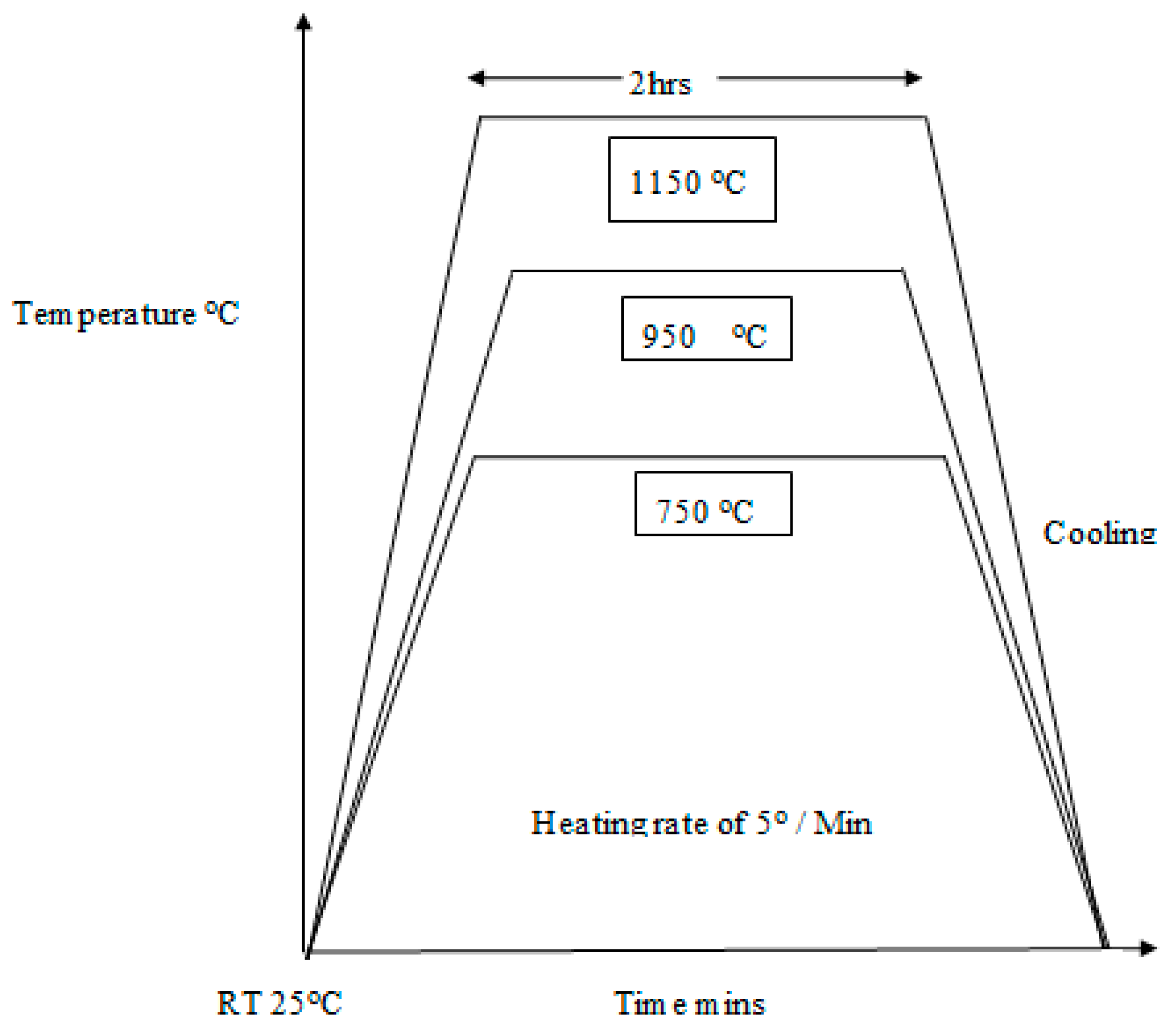
2.2. Bulk Alloy Preparation by the Crystal Growth Technique

Appropriate weights of In and Ga metals were mixed and put in a clean silica ampoule closed from one side in order to produce InxGa1−xN bulk alloys with different compositions (x = 0.1, 0.3, 0.5, 0.7 and 0.9). The ampoule was then evacuated from the other side at a pressure of 10−4 Torr and sealed by welding the narrow nick which was made to insert NH3, as shown in Figure 1a. The flow rate of ammonia was 0.1 sccm for 7 min. The growth of the bulk alloys was prepared with various compositions of 0.1, 0.3, 0.5, 0.7, and 0.9 for In metal, at various temperatures of 750 °C, 950 °C and 1150 °C. The resulting alloy composite was cooled slowly to ambient temperature in order to prevent segregation, as shown in Figure 1b. The reaction schedule can be schematically represented in Figure 2 and explained by these equations as follows:
Ga (Jelly) + NH3 ⟶ GaN(s) + 3/2H2
In (Metal) + NH3⟶InN(s) + 3/2H2

2.3. Preparation of Doped Alloys by the Crystal Growth Technique

2.3.1. Preparation of In0.1Ga0.9N: Mg [p-type]

The weighted elements, i.e., In and Ga metals, were put in a silica tube under NH3 gas with the addition of 0.02% Mg as a p-type dopant to prepare In0.1Ga0.9N: Mg under a growth temperature of 750 °C with a temperature rise of 5 °C/min. After reaching 750 °C, it was raised to 800 °C and stayed at this temperature for 30 min, then it was cooled to 530 °C for 20 min with the muffle off, allowing the sample to be cooled.

2.3.2. Preparation of In0.1Ga0.9N: Zn [n-type]

The weighted elements, i.e., In and Ga metals, were put in a silica tube under NH3 gas with 0.02% Zn. The elements reached 800 °C and stayed at this temperature for 1 h and then the muffle furnace was cooled to room temperature.

2.3.3. Preparation of Bulk Buffer GaN Alloy

The weighed gallium element with 0.1 gm. was put in the vacuumed silica tube filled with NH3 gas. The tube was kept at 950 °C for 2 h then the muffle was cooled to room temperature.

3. Results

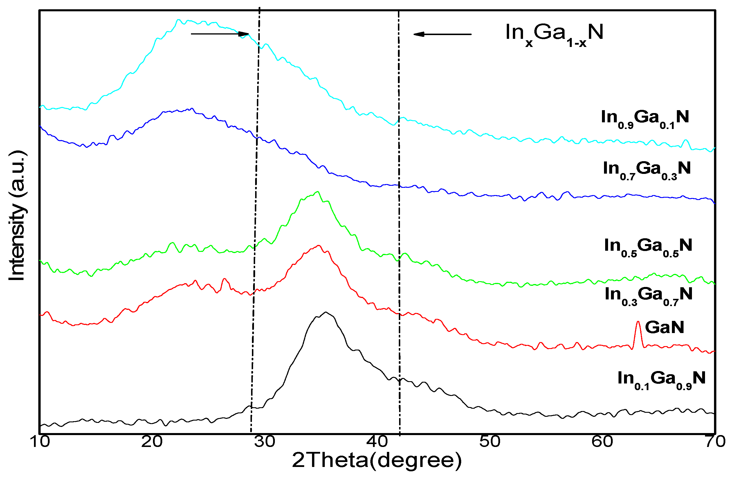
3.1. X-ray Diffraction

3.1.1. For InxGa1−xN Alloys Prepared at Different Compositions

Figure 3 shows XRD patterns for InxGa1−xN alloys prepared at different compositions of In (x = 0.1, 0.3 0.5, 0.7 0.9) at a heating temperature of 950 °C for 2 h. As the indium composition increases, a shift in the 2θ value from 33o to 23o and broadening of the main peak is observed. This confirms a change of indium content according to the corresponding 2θ value of the same crystallographic planes (002), (100) and (101) with respect to that of InN (JCPDS Card No: 01-088-2365) and GaN (JCPDS No: 00-052-0871) [16]. Therefore, the formation of the InxGa1−xN phase is obtained in the range of 2θ between approximately 31° and 37° [17]. When the In composition increases from 0.1 to 0.5, the same diffraction peaks are observed between 30.73° and 37.77°, which matches with some previous studies [18,19]. This indicates a good structure quality and orientations of InxGa1−xN alloys. As the indium composition increases to 0.7 and 0.9, the peaks shift to InN with a wurtzite structure (hexagonal). In In0.3Ga0.7N, there is an additional peak at 67.3° which belongs to the GaN structure with respect to that of InN (JCPDS Card No: 00-050-0792). It refers to the phase separation that is only found in this composition [20]. The broadening of the peaks might arise from several factors such as the distribution of bond lengths for a random alloy size-dependent broadening, the large size of the X-ray beam spot across the composition gradient and the inhomogeneity of the ternary InxGa1−xN alloys [21].

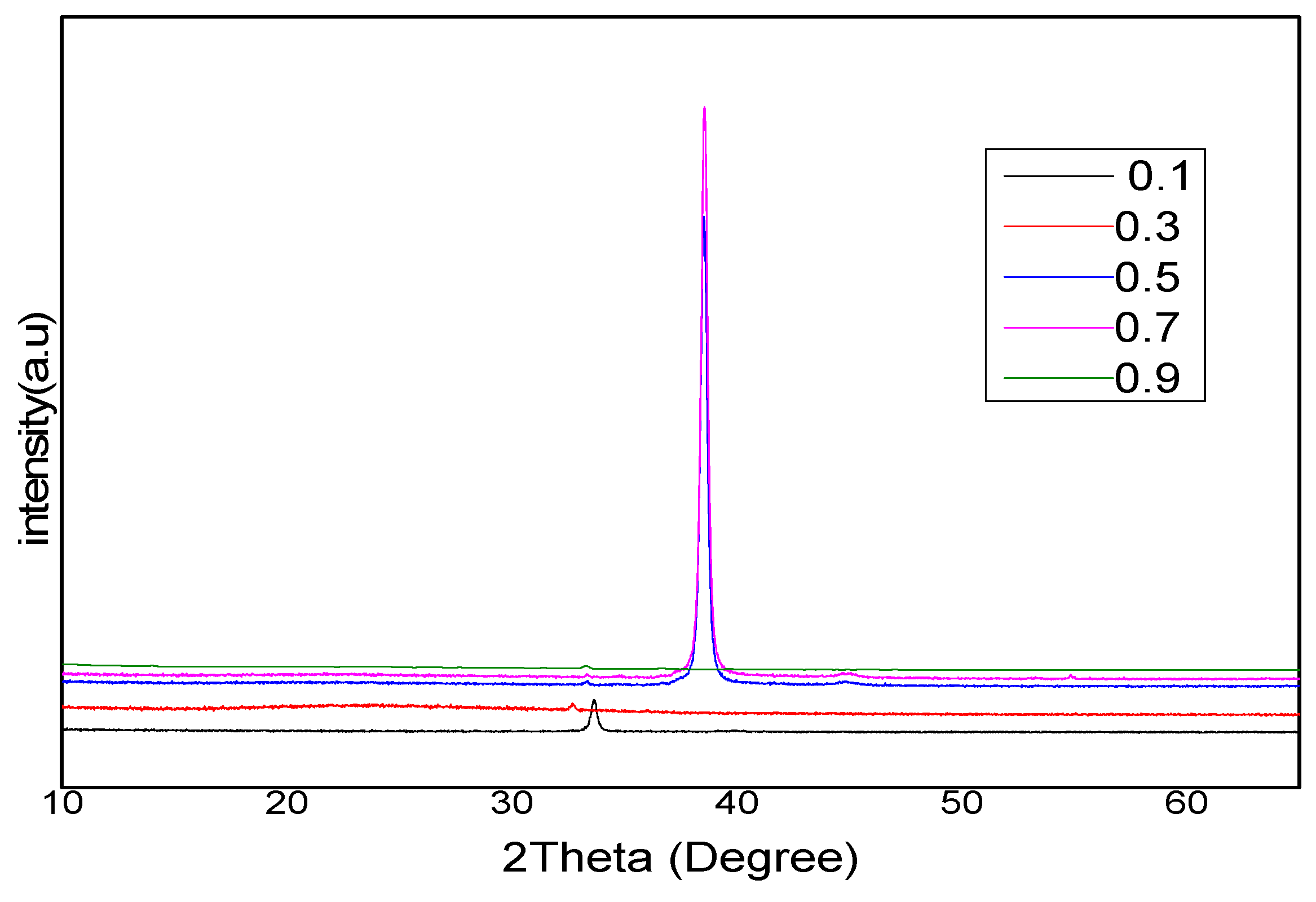
3.1.2. InxGa1−xN Thin Film Deposited by TVE at Different Compositions

Figure 4 shows the XRD patterns of InxGa1−xN thin films deposited by thermal vacuum evaporation (TVE). InxGa1−xN thin films grown on glass at x = 0.1, 0.3, 0.9 have diffraction peaks of 33°, 32° and 33°, respectively, with a hexagonal structure as matched with ref [22]. At x = 0.5 and 0.7, the diffraction angle is obtained at 2θ of 38° with the cubic structure that matched with ref [23]. No extra peaks were observed in all samples and it may mean that no In droplets or phase separation was observed from the InxGa1−xN layers [24]. This indicates a good structure quality and orientation.

3.2. Compositional Analysis

3.2.1. Bulk Alloys and Thin Film at Different Compositions Prepared by TVE
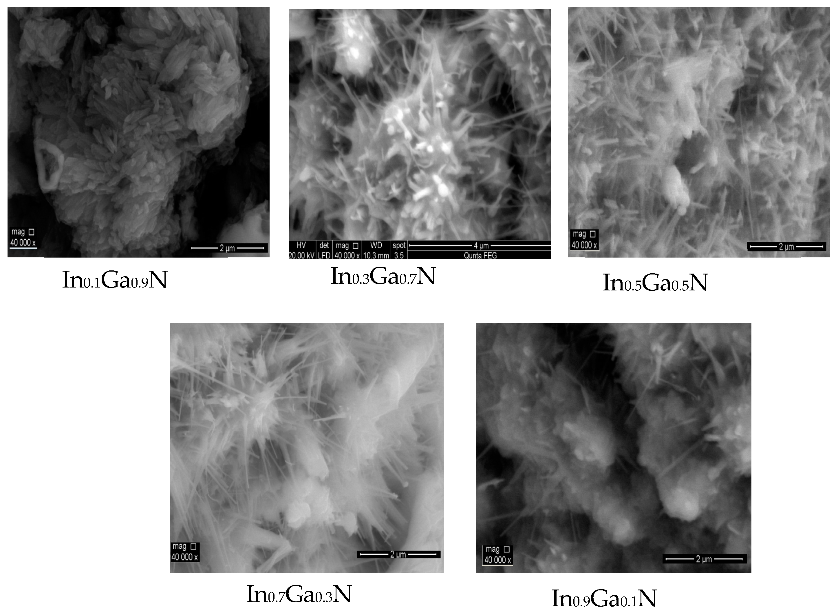
The comparison between the theoretical calculated composition of InxGa1−xN bulk alloys, and thin films weighed before preparation, and the measured composition by the EDX is represented in Table 1. It is noted that there is no great difference of values between thermal vacuum deposited thin films and bulk alloys in their chemical composition with respect to the nominal weighted materials. This indicates that the composition is well controlled by the used preparation techniques. The ratio of nitrogen in both bulk and thin films shows that there is no change across the two techniques except for bulk composition at x = 0.5 and thin film at x = 0.1.

3.3. Morphology

3.3.1. Bulk Alloys with Different Compositions Prepared by Crystal Growth

Figure 5 shows FESEM images for bulk alloys at InxGa1−xN heated at 950 °C (0.1≤ x ≤ 0.9) and it demonstrates clearly distinct nanowires in the bulk alloys with increasing indium incorporation.
The nanowires show a high degree of order. As the indium composition increases, the widening of the nanowire’s diameter and length decreases significantly, as seen in Table 2.

3.3.2. Thin Films Prepared by TVE at Different Compositions Deposited on Glass

Figure 6 shows the FESEM for thin films of InxGa1−xN deposited by thermal vacuum evaporation. It is noted that surface morphologies of the InxGa1−xN films with different indium compositions have a smooth surface with homogenous nano-spherical sized particles of the films. At x = 0.1, the thin film is denser than the other compositions and exhibits good surface morphologies. The average diameter of the particle size decreases as the In composition increases.
Table 3 shows the particle size that was measured from FESEM images which has little difference compared to the size calculated from Scherer’s equation. It ranged from about 35 nm at x = 0.1 to 22 nm at x = 0.9. The observed larger grain sizes are composed of fine nanoparticles and some grains of about 500 nm at x = 0.1, 0.3, which decreased to about 290 nm at x = 0.5, 0.7 and 0.9.

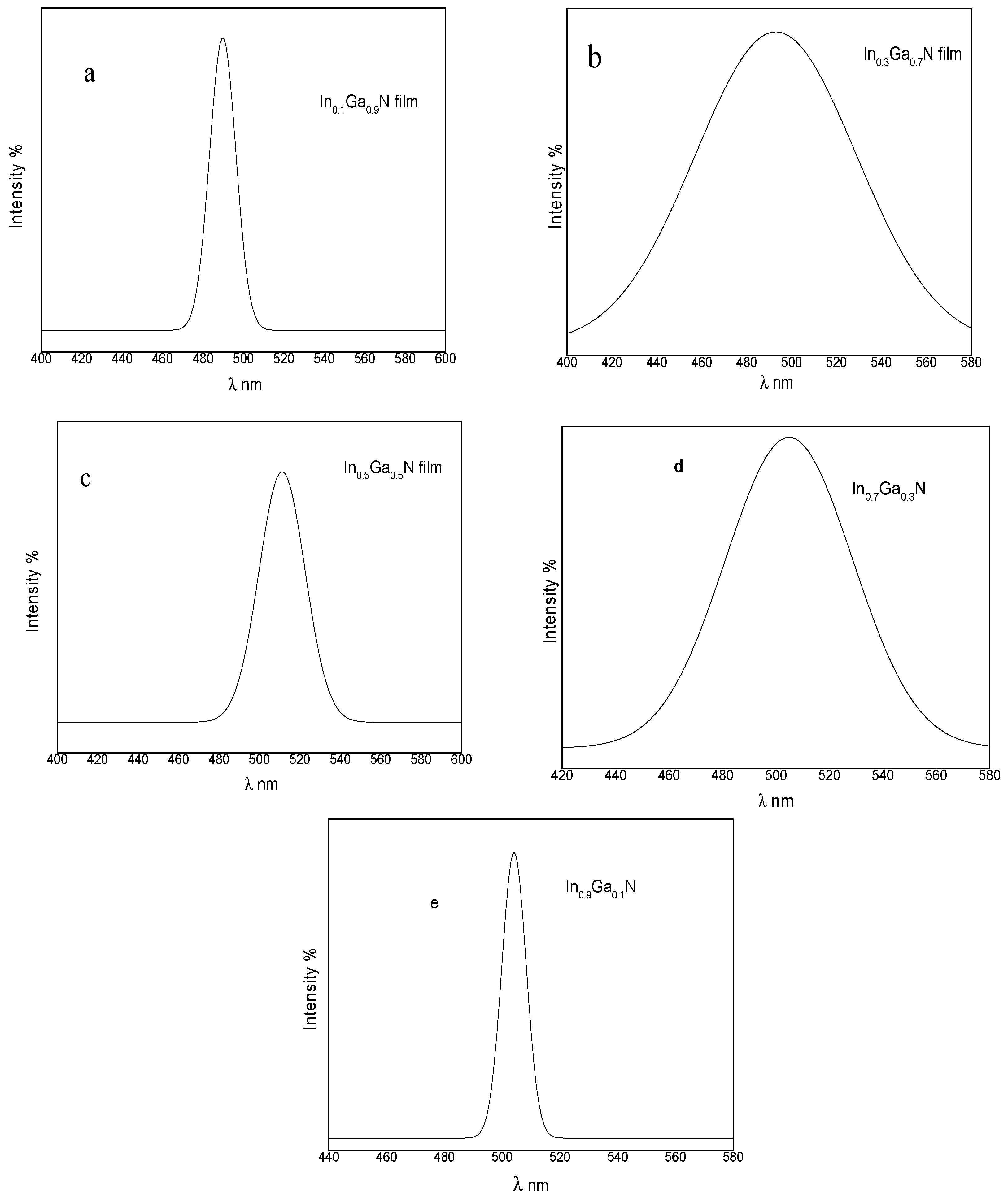
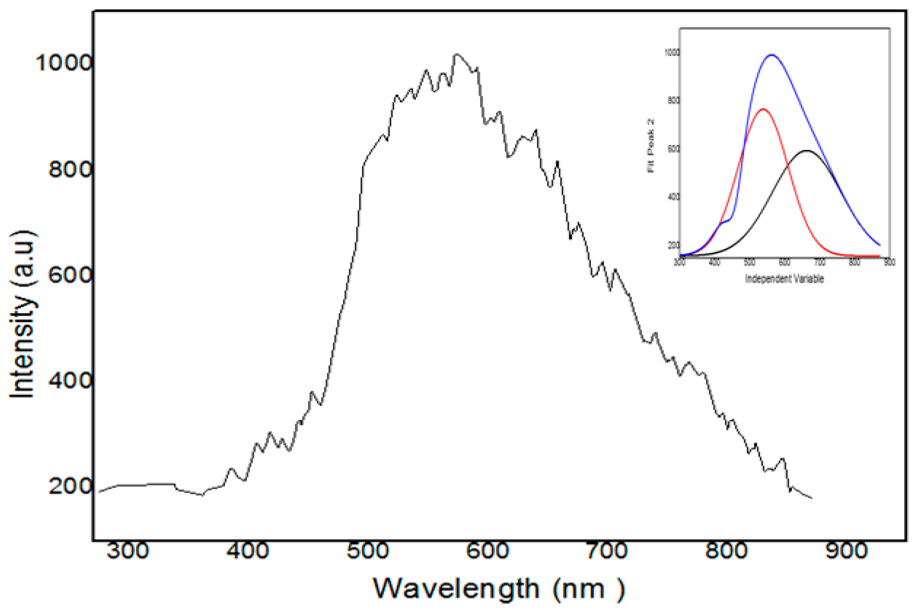
3.4. Optical Properties for Thin Films

Photoluminescence (PL) Thin Films Prepared by Thermal Vacuum Evaporation

The PL emission for thin films of InxGa1−xN deposited by thermal vacuum evaporation is shown in Figure 7. No extra PL emission peaks are observed with different composition contents. The observed optical emission at room temperature is attributed to radiative band-to-band transitions. A red shift of the optical emission with increasing Indium content is observed [25] and this ranged from 2.6 nm to 2.4 nm. Also, the widening of the peaks for compositions of x = 0.3, 0.7 may be due to the lowest states of the conduction band being blocked, a phenomenon known as the Burstein–Moss effect [25], which occurs with an increase in the carrier density. The narrowing of the peaks for compositions 0.1, 0.5, and 0.9 may be due to the crystallinity and homogeneity of the thin films, as shown by XRD data [25]. In order to determine the band gap of all samples, each PL spectrum was fitted by a Gaussian distribution function, as shown in Figure 7. The band gap values were directly obtained from the maximum of the PL peaks, as shown in Table 4. The band gap values obtained from the PL measurements were of the same order of magnitude as is found in a variety of InxGa1−xN alloys [26,27,28,29]. In the case of bulk alloys, the bandgap values at an In content of 0.1 and 0.3 were compatible with the InxGa1−xN system. The thin films prepared by TVE and the small bandgap values at x = 0.5, 0.7 and 0.9, as shown in Table 4, refer to a possible phase separation in the bulk alloys which is previously explained by the XRD data presented in Figure 3.
The calculation of the bowing parameter, as shown in Table [3.1], depends on Vegard’s law [30]:
Eg (InxGa1−xN) = Eg GaN (1 − x) + Eg InN(x) − bx (1 − x)
where Eg(GaN) = 3.4 eV, Eg(InN) = 0.7 eV and b = bowing parameter
In bulk alloys, the bowing calculations show large values at (x = 0.1 and 0.3), except for (x = 0.5, 0.7 and 0.9) which have small values. As shown in Table 4, the highest bandgap bowing parameter is (b = 2.89 eV) for bulk alloys. In thin films prepared by TVE, the bowing values are decreased as the composition increases. Since the InxGa1−xN alloys are highly disordered crystal systems, there are large differences in the lattice constants between GaN and InN [31]. Due to this disordered crystal geometry, it is possible to undergo metamorphosis of physical properties, such as band-structure deformation.

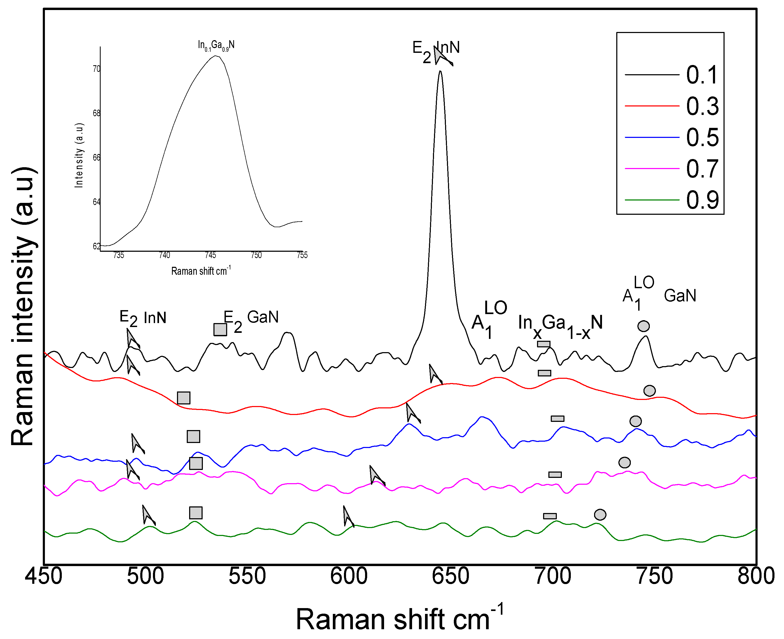
3.5. Raman Spectroscopy

3.5.1. In0.1Ga0.9N Thin Films Deposited by Thermal Vacuum Evaporation

It has been established that the InxGa1−xN thin films exhibit two modes of behavior, i.e., the Raman spectrum consists of the A1LO and E2 lines which vary in frequency between those of the two binary compounds InN and GaN [32]. The Raman measurements of the InxGa1−xN thin films were made at room temperature in the backscattering configuration. The spectrum recorded at the excitation wavelength is λexc = 530 nm. Raman spectra from InxGa1−xN thin films (x = 0.1, 0.3, 0.5, 0.7 and 0.9) are displayed in Figure 8. The InN, GaN and InxGa1−xN are stable in the hexagonal wurtzite phase, in which their scattering at the E2 and A1LO phonons is allowed. The frequency values of GaN at A1LO = 734 cm−1 and E2 = 568 cm−1, 570 cm–1, while the frequency values of the InN A1LO = 586 cm−1, and E2 = 488cm−1. Also, there is a phonon band in the frequency region of the A1LO InxGa1−xN vibrations (700–750 cm–1). The observed behavior of the modes is reported in several previous works [33]. In (x = 0.3, 0.5, 0.7 and 0.9) compositions, there is a shift of the frequency and high broadening due to elastic strain between the thin film and glass substrate, and also due to high Indium content [34].

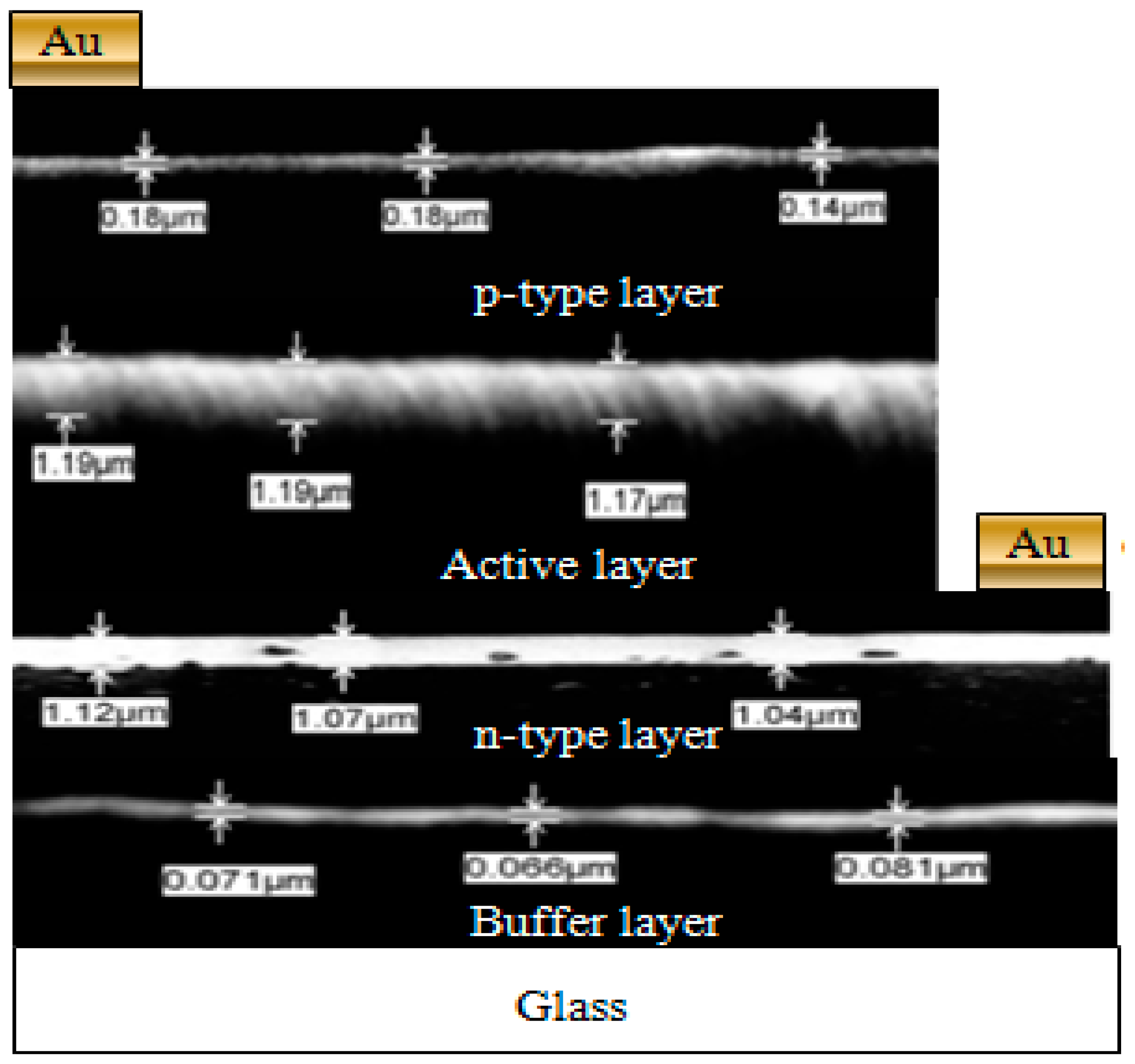
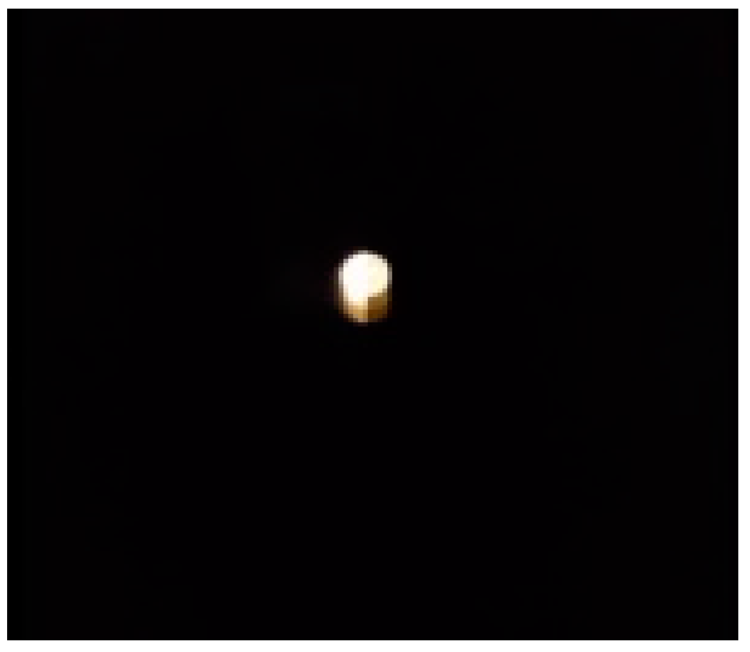
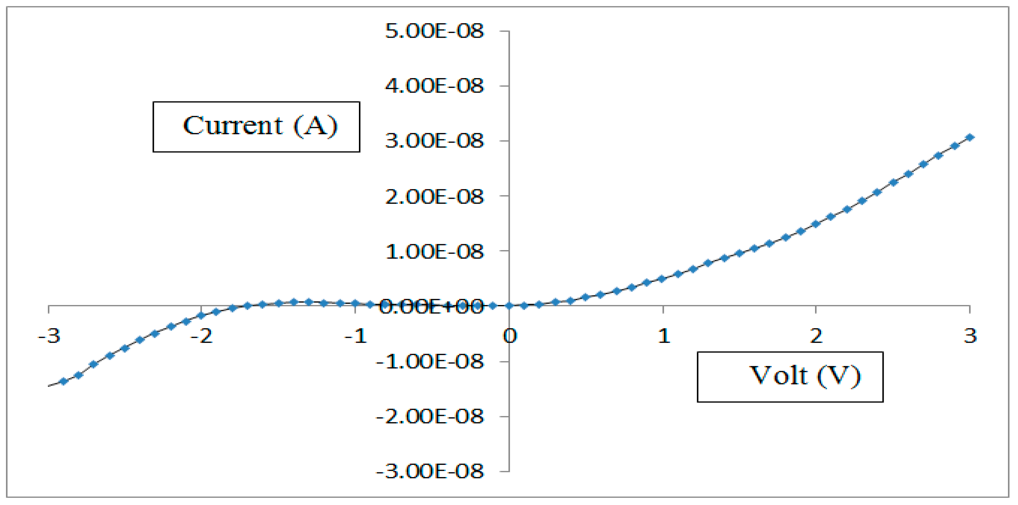
3.6. Device Fabrication

3.6.1. Device Characterizations

LED layered devices with a configuration of Glass/GaN/In0.1Ga0.9N:Zn/In0.1Ga0.9N/In0.1Ga0.9N: Mg were deposited on glass by thermal vacuum evaporation. The cross-sectional FESEM images of these devices are given in Figure 9. These images show the regular and uniform thickness of each layer, which is found to be 0.072 µm for the buffer layer (GaN), 1.07 µm for the n-type layer In0.1Ga0.9N, 1.18 µm for the active layer (In0.1Ga0.9N), and 0.167 µm for the p-type layer In0.1Ga0.9N. The FESEM results showed that the thicknesses of the GaN buffer layer were less than the values of all LED layers. This structure generates a white light for the first time and is shown in Figure 10, which is taken by a digital camera during the light emission.
The EL spectra, as shown in Figure 11, show that InxGa1−xN is shaped as a wide spectrum in the 300–900 nm range. The EL spectra for the LED structure contain glass/GaN/In0.1Ga0.9N: Zn/In0.1Ga0.9N/In0.1Ga0.9N: Mg coated by Au at both sides of p and n types, forming the InxGa1−xN LED structure. The use of Gaussian line shapes allowed the discrimination of three overlapping luminescence-using bands with their maximums at 426 nm, 548 nm, and 599 nm respectively. The shorter wavelength in the range of 402 to 426 nm may be due to two reasons. Firstly, it may be due to the In0.1Ga0.9N deposited on GaN which gives blue emission spectra. This blue emission of EL spectra suggests that the luminescence mechanism is in donor–acceptor transition in the In0.1Ga0.9N active layer co-doped with Zn. The In0.1Ga0.9N active layer of the blue spectra is doped with Zn. Thus, the Zn acceptor level is expected to exhibit Gaussian broadening and both the valence band and the conduction band will have band tails [35,36]. The shorter wavelength at 548 nm may be due to the p-type doping which gives green emission [37]. The EL curve of the device shows a green peak emission, which implies that the recombination of holes and electrons occurs predominantly in the green light near the p- In0.1Ga0.9N layer. This phenomenon indicates that the Mg doping concentration of the sample has little effect on hole injection into the LED structure. So, most holes are trapped in the green emission due to their lower mobility than that of electrons in the In0.1Ga0.9N/GaN. Due to Mg doping into the material, the recombination of holes and electrons occurred [38,39]. There is a yellow band at 560 nm [40] that may belong to GaN and a new red band near 620 nm which may be due to a recombination via deep levels in In0.1Ga0.9N. The violet band at 410 nm can be ascribed to a donor–acceptor pair recombination in the GaN. According to the InxGa1−xN structure, a blue emission originating from a recombination in the InxGa1−xN: Mg deposited on the InxGa1−xN layer and shifted toward a short wavelength (599 nm). Since the mobility of electrons is faster than holes, electrons are injected from the n- InxGa1−xN: Zn side, through the InxGa1−xN layer, to the p- InxGa1−xN: Mg side and little recombination occurred in the n- InxGa1−xN and InxGa1−xN layers. Thus, the blue emission peak at 599 is observed [41].
Figure 12 shows the room temperature I–V curve (under dark) measured by two electrodes Potentionstat Auto Lab. 70,708 with the positive electrode of the electric source connected to the Au metal contact upon the In0.1Ga0.9N LED. The results show that the diode has rectifying current characteristics with a current density of 1.2 × 10⁻⁷ A/cm2 for the diode area of 0.25 cm2 [42].

4. Conclusions

This research focused on the growth of InxGa1−xN as bulk alloys and thin films which work as an active layer in LED devices. The alloy growth was carried out in a programmable muffle using an evacuated silica tube with appropriate amounts of In and Ga metals under high purity ammonia gas. The optimized growth temperature of the bulk alloy was 950 °C with a strong PL peak energy of 2.65 eV at composition (x) = 0.1. The work also includes the doping of In0.1Ga0.9N by the crystal growth technique for both n and p type using Zn and Mg, respectively. XRD was used to detect the growth of the grown bulk alloys and thin films exhibiting high crystallinity and no phase separation in most of them. Additionally, the novelty of this work is the use of a glass substrate, which is cheaper than sapphire. The LED device was glass/GaN/In0.1Ga0.9N:Zn/In0.1Ga0.9N/In0.1Ga0.9N: Mg, coated by Au at the p and n type layers which worked as metal electrodes. The In0.1Ga0.9N-based white LED layer structure was fabricated using a thermal vacuum evaporator. The output emission was a white light and was verified by EL spectroscopy. We believe that this study, which involved preparing In0.1Ga0.9N as an active layer of blue emission and generating a white light with In0.1Ga0.9N LEDs, offers a way to realize a low-cost technique for such highly needed devices globally.

Author Contributions

Conceptualization, A.E.-H.B.K. and M.F.; Investigation, A.E.-H.B.K., M.F. and S.G.; Methodology, M.F., S.G.; Supervision, A.E.-H.B.K., M.F. and Y.B.; Visualization, Y.B. and A.A.B.; Writing—review & editing, A.E.-H.B.K., M.F. and S.G.

Funding

This research received no external funding.

Acknowledgments

This work was carried out at City for Scientific Research and Technological Applications (SRTA-City) and collaboration research with the National Institute of Laser Enhanced Science.

Conflicts of Interest

The authors declare no conflict of interest.

References

  1. Ekinci, H.; Kuryatkov, V.; Forgey, C.; Dabiran, A.; Jorgenson, R.; Nikishin, S. Properties of InGaN/GaN MQW LEDs grown by MOCVD with and without hydrogen carrier gas. Vacuum 2018, 148, 168–172. [Google Scholar] [CrossRef]
  2. Mokhov, E.N.; Wolfson, A.A. Single Crystals of Electronic Materials; Woodhead Publishing: Cambridge, UK, 2019; pp. 401–445. [Google Scholar]
  3. Jung, B.O.; Bae, S.Y.; Kim, S.Y.; Lee, S.; Lee, J.Y.; Lee, D.S.; Kato, Y.; Honda, Y.; Amano, H. Highly ordered catalyst-free InGaN/GaN core–shell architecture arrays with expanded active area region. Nano Energy 2015, 11, 294–303. [Google Scholar] [CrossRef]
  4. Al-Khanbashi, H.A.; Almarwani, A.M. Evaluation of the optical properties of the InGaN/GaN quantum well nanopillar arrays prepared via MOVPE approach. Optika 2018, 164, 28–35. [Google Scholar] [CrossRef]
  5. Zimmermann, F.; Beyer, F.C.; Gärtner, G.; Röder, C.; Son, N.T.; Janzén, E.; Veselá, D.; Lorinčík, J.; Hofmann, P.; Krupinski, M.; et al. Origin of orange color in nominally undoped HVPE GaN crystals. Opt. Mater. 2017, 70, 127–130. [Google Scholar] [CrossRef]
  6. Jennifer, K.H.; Travis, J.A.; Lunet, E.L.; James, C.G.; Charles, R.E. Influence of HVPE substrates on homoepitaxy of GaN grown by MOCVD. J. Cryst. Growth 2018, 498, 352–356. [Google Scholar]
  7. Tomasz, S.; Zachary, B.; Mikolaj, A.; Milena, B.; Michal, F.; Isaac, B.; Boleslaw, L.; Ramon, C.; Weyher, J.; Kucharski, R.; et al. HVPE-GaN grown on MOCVD-GaN/sapphire template and ammonothermal GaN seeds: Comparison of structural, optical, and electrical properties. J. Cryst. Growth 2014, 394, 55–60. [Google Scholar]
  8. Ariff, A.; Ahmad, M.A.; Hassan, Z.; Zainal, N. Influence of ammonia flow rate for improving properties of polycrystalline GaN. Superlattices Microstruct. 2018, 118, 130–136. [Google Scholar] [CrossRef]
  9. Loganathan, R.; Baskar, K. Epitaxial growth of AlN microwalls on wet etched GaN template by MOCVD. Superlattices Microstruct. 2018, 123, 144–153. [Google Scholar]
  10. Mickevičius, J.; Dobrovolskas, D.; Steponavičius, T.; Malinauskas, T.; Kolenda, M.; Kadys, A.; Tamulaiti, G. Engineering of InN epilayers by repeated deposition of ultrathin layers in pulsed MOCVD growth. Appl. Surf. Sci. 2018, 427, 1027–1032. [Google Scholar] [CrossRef]
  11. Bagavath, C.; Lucía, N.; Jitendra, S.K. Investigations on the nanostructures of GaN, InN and InxGa1−xN. Mater. Sci. Semicond. Process. 2016, 72, 61–67. [Google Scholar] [CrossRef]
  12. Teles, L.K.; Marques, M.; Scolfaro, L.M.R.; Leite, J.R. Phase Separation and Ordering in Group-III Nitride Alloys. J. Braz. Phys. 2004, 34, 593–597. [Google Scholar] [CrossRef]
  13. Pengfei, L.; Dan, L.; Chunfang, Z.; Ruge, Q.; Shumin, W. Closing the bandgap for III-V nitrides toward mid-infrared and THz applications. Sci. Rep. 2017, 7, 10594. [Google Scholar]
  14. Osamura, K.; Naka, S.; Murakami, Y. Preparation and optical properties of Ga1−xInxN thin films. J. Appl. Phys. 1975, 46, 3432. [Google Scholar] [CrossRef]
  15. Clinton, E.A.; Vadiee, E.; Fabien, C.A.; Moseley, M.W.; Gunning, B.P.; Doolittle, W.A.; Fischer, A.M.; Wei, Y.O.; Xie, H.; Ponce, F.A. A review of the synthesis of reduced defect density InxGa1−xN for all indium compositions. Solid-State Electron. 2017, 136, 3–11. [Google Scholar] [CrossRef]
  16. Itoh, T.; Hibino, S.; Sahashi, T.; Kato, Y.; Koiso, S.; Ohashi, F.; Nonomura, S. InXGa1−xN films deposited by reactive RF-sputtering. J. Non-Cryst. Solids 2012, 358, 2362–2365. [Google Scholar] [CrossRef]
  17. Pavel, S.; Goloshchapov, D.; Lenshin, A.; Mizerov, А.М.; Zotolukhin, D.S. Influence of por-Si sublayer on the features of heteroepitaxial growth and physical properties of InxGa1−xN/Si(111) heterostructures with nanocolumn morphology of thin film. Phys. E Low Dimens. Syst. Nanostruct. 2017, 413, 62–67. [Google Scholar]
  18. Guarneros, J.E.; Sánchez, V.M.; López, U. Study of InxGa1−xN layers growth on GaN/Al2O3 by MOCVD at different pressures. Superficies y Vacío 2013, 26, 107–110. [Google Scholar]
  19. Tomasz, J.O.; Bernard, G.; Pierre, L. Photoreflectance investigations of the bowing parameter in AlGaN alloys lattice-matched to GaN. Appl. Phys. Lett. 1999, 74, 3353. [Google Scholar]
  20. Okada, N.; Inomata, Y.; Ikeuchi, H.; Fujimoto, S.; Itakura, H.; Nakashima, S.; Kawamura, R.; Tadatomo, K. Characterization of high-quality relaxed flat InGaN template fabricated by combination of epitaxial, lateral overgrowth and chemical mechanical polishing. J. Cryst. Growth 2019, 512, 147–151. [Google Scholar] [CrossRef]
  21. Song, A.Y.; Bhat, R.; Allerman, A.A.; Wang, J.; Huang, T.Y.; Zah, C.E.; Gmachl, C.F. Quantum cascade emission in the III-nitride material system designed with effective interface grading. Appl. Phys. Lett. 2015, 107, 132104. [Google Scholar] [CrossRef]
  22. Pereira, S.; Correia, M.R.; Monteiro, T.; Pereira, E.; Alves, E.; Sequeira, A.D.; Franco, N. Compositional dependence of the strain-free optical band gap in InxGa1−xN layers. Appl. Phys. Lett. 2001, 78, 21–37. [Google Scholar] [CrossRef]
  23. Xue, J.J.; Chen, D.J.; Liu, B.; Lu, H.; Zhang, R.; Zheng, Y.D.; Cui, B.; Andrew, M.W.; Amir, M.D.; Xu, K.; et al. Indium-rich InGaN epitaxial layers grown pseudomorphically on a nano-sculpted InGaN template. Opt. Express. 2012, 20, 8093–8099. [Google Scholar] [CrossRef] [PubMed]
  24. Baş, Y.; Demirel, P.; Akın, N.; Başköse, C.; Özen, Y.; Kınacı, B.; Öztürk, M.; Özçelik, S.; Özbay, E. Microstructural defect properties of InGaN/GaN blue light emitting diode structures. J. Mater. Sci.-Mater. Electron. 2014, 25, 3924–3932. [Google Scholar]
  25. Ramos-Carrazco, A.; Chaikina, E.; Contreras, O.E.; Barboza-Flores, M.; Garcia, R. Structural and optical characterization of InxGa1−xN nano-structured grown by chemical vapor deposition. Rev. Mex. Fis. 2011, 57, 7–9. [Google Scholar]
  26. Strocov, V.N.; Schmitt, T.; Rubensson, J.E.; Blaha, P.; Paskova, T.; Nilsson, P.O. Band structure effects in nitrogen K–edge resonant inelastic X–ray scattering from GaN. Phys. Status Solidi 2004, 241, R27–R29. [Google Scholar] [CrossRef]
  27. Chen, X.; Matthews, K.D.; Hao, D.; Schaff, W.J.; Eastman, L.F. Growth, fabrication, and characterization of InGaN solar cells. Phys. Status Solidi (a) 2008, 205, 1103–1105. [Google Scholar] [CrossRef]
  28. Yildiza, A.; Dagdelenb, F.; Acarc, S.; Lisesivdinc, S.B.; Kasapc, M.; Aydogdub, Y.; Bosid, M. Stokes Shift and Band Gap Bowing in InxGa1−xN (0.060 ≤ x ≤ 0.105) Grown by Metalorganic Vapour Phase Epitaxy. Acta Phys. Pol. 2008, 113, 731–739. [Google Scholar] [CrossRef]
  29. Mohamed, F.; Bechstedt, F. First-principles calculations of gap bowing in InxGa1−xN and InxAl1−xN alloys: Relation to structural and thermodynamic properties. Phys. Rev. B 2002, 65, 075213. [Google Scholar]
  30. Xing, Z.; Yang, W.; Yuan, Z.; Li, X.; Wu, Y.; Long, J.; Jin, S.; Zhao, Y.; Liu, T.; Bian, L.; et al. Growth and characterization of High In-content InGaN grown by MBE using Metal modulated epitaxy technique (MME). J. Cryst. Growth 2019, 516, 57–62. [Google Scholar] [CrossRef]
  31. Hernánde, C.A.; Yuriy, K.; Dagoberto, C.; Guillén, A.; Santana, G.; Arturo, E.E.E.; Luis, H.H.; Maximo, L.L. InxGa1−xN nucleation by In+ ion implanation into GaN. Nucl. Instrum. Methods Phys. Res. B 2017, 413, 62–67. [Google Scholar]
  32. Hernandez, S.; Cusco, R.; Pastor, D.; Artus, L.; ODonnell, K.P.; Martin, R.W.; Watson, I.M.; Nanishi, Y.; Calleja, E. Raman-scattering study of the InGaN alloy over the whole composition range. Appl. Phys. 2005, 98, 013511. [Google Scholar] [CrossRef]
  33. Strelchuk, V.V.; Kladko, V.P.; Avramenko, E.A.; Kolomys, O.F.; Safryuk, N.V.; Konakova, R.V.; Yavich, B.S.; Valakh, M.Y.; Machulin, V.F.; Belyaev, A.E. Diffraction Analysis and Scanning Micro_Raman Spectroscopy the Multilayered InGaN/GaN Heterostructure. Fizika i Tekhnika Poluprovodnikov 2010, 44, 1236–1247. [Google Scholar]
  34. Lin, C.H.; Kuo, H.C.; Lai, C.F.; Huang, H.W.; Leung, K.M.; Yu, C.C.; Lo, J.R. Light extraction enhancement of InGaN-based green LEDs with a composite omni- directional reflector. Semicond. Sci. Technol. 2006, 21, 1513–1517. [Google Scholar] [CrossRef]
  35. Kang, M.S.; Lee, C.H.; Park, J.B.; Yoo, H.; Yi, G.C. Gallium nitride nanostructures for light-emitting diode applications. Nano Energy 2012, 1, 391–400. [Google Scholar] [CrossRef]
  36. Sheu, J.K.; Pan, C.J.; Chi, G.C.; Kuo, C.H.; Wu, L.W.; Chen, C.H.; Chang, S.J.; Su, Y.K. White-light emission from InGaN/GaN multi-quantum well light-emitting diodes with Si and Zn co doped active layer. IEEE Photonic Technol. Lett. 2002, 14, 450–452. [Google Scholar] [CrossRef]
  37. Reshchikov, M.A.; McNamar, J.D.; Helava, H.; Usikov, A.; Makarov, A. Two yellow lumincess bands in undoped GaN. Sci. Rep. 2018, 8, 8091. [Google Scholar] [CrossRef] [PubMed]
  38. Chuo, C.C.; Lee, C.M.; Chyi, J.I. Inter diffusion of In and Ga in InGaN/GaN multiple quantum wells. Appl. Phys. Lett. 2001, 78, 314–316. [Google Scholar] [CrossRef]
  39. Chang, S.J.; Wu, L.W.; Su, Y.K.; Kuo, C.H.; Lai, W.C.; Hsu, Y.P.; Sheu, J.K.; Chen, J.F.; Tsai, J.M. Si and Zn Co-Doped InGaN–GaN White Light-Emitting Diodes. IEEE Trans. Electron Devices 2003, 50, 519–521. [Google Scholar] [CrossRef]
  40. Kunert, H.W.; Brink, D.J.; Auret, F.D.; Maremane, M.; Prinsloo, L.C.; Barnas, J.; Beaumont, B.; Gibart, P. Photoluminescence and Raman spectroscopy of Mg-doped GaN as grown, hydrogen implanted and annealed. Mater. Sci. Eng. B 2003, 102, 293–297. [Google Scholar] [CrossRef]
  41. Ti, W.; Hao, W.; Zheng, W.; Chao, C.; Chang, L. Blue light emission from the heterostructured ZnO/InGaN/GaN. Nano Exp. 2013, 8, 99. [Google Scholar]
  42. Sun, X.; Liu, W.B.; Jiang, D.S.; Liu, Z.S.; Zhang, S.; Wang, L.L.; Wang, H.; Zhu, J.J.; Duan, L.H.; Wang, Y.T. Photoelectric characteristics of metal / InGaN/ GaN heterojunction. Appl. Phys. 2008, 41, 165108. [Google Scholar] [CrossRef]
Figure 1. (a) Experimental setup. The tube contains In and Ga metals and NH3 gas. (b) The resulting indium gallium nitride (InxGa1−xN) alloy after reaction.
Photonics 06 00044 g001
Figure 2. Schematic diagram for the growth process of the InxGa1−xN alloy under different temperatures.
Photonics 06 00044 g002
Figure 3. X-Ray diffraction (XRD) patterns of the bulk InxGa1−xN alloy at different In compositions (x = 0.1, 0.3, 0.5, 0.7, 0.9) prepared at 950 °C for 2 h.
Photonics 06 00044 g003
Figure 4. XRD patterns of InxGa1−xN (x = 0.1, 0.3, 0.5, 0.7 and 0.9) thin films deposited on glass substrates using thermal vacuum evaporation (TVE).
Photonics 06 00044 g004
Figure 5. Field emission scanning electron microscopy (FESEM) for bulk alloys at InxGa1−xN heated at 950 °C (0.1 ≤ x ≤ 0.9).
Photonics 06 00044 g005
Figure 6. FESEM for InxGa1−xN thin films prepared with TVE for the alloy prepared at 950 °C.
Photonics 06 00044 g006
Figure 7. PL-spectra of InxGa1−xN thin films deposited at (0.1 ≤ x ≤ 0.9).
Photonics 06 00044 g007
Figure 8. Raman spectroscopy of InxGa1−xN thin film prepared by TVE at different x ratios.
Photonics 06 00044 g008
Figure 9. Cross-section of the In0.1Ga0.9N LED.
Photonics 06 00044 g009
Figure 10. White light generated from the In0.1Ga0.9N LED.
Photonics 06 00044 g010
Figure 11. Electroluminescence of the cross-section of the In0.1Ga0.9N LED.
Photonics 06 00044 g011
Figure 12. I–V curve of the cross-section of the In0.1Ga0.9N LED.
Photonics 06 00044 g012
Table 1. Energy dispersive X-ray spectroscopy technique (EDX) measurements of InxGa1−xN bulk alloys and thin films.
InxGa1−xN Bulk AlloysThin Films
In%Ga%N% In%Ga%N%
In0.1Ga0.9N11.4686.022.5217.4160.7321.85
In0.3Ga0.7N27.364.28.531.0663.785.17
In0.5Ga0.5N42.9040.7016.448.0544.777.18
In0.7Ga0.3N67.7825.516.760.6732.656.68
In0.9Ga0.1N88.029.462.5282.67 13.41 3.92
Table 2. Measurements of nanowire diameter and length from FESEM for InxGa1−xN bulk alloys.
Composition of InxGa1−xN Bulk Alloy
(x%)
Bulk Alloy Deposited on Glass
Length
(nm)
Diameter
(nm)
0.134169
0.317649
0.51539.1
0.71427.7
0.91044.25
Table 3. The particle size measurements from FESEM and Scherer’s equation for thin films deposited on a glass substrate.
Composition of InxGa1−xN Thin FilmsParticle Size (nm) from FESEMCrystallite Size (nm) from XRD
0.135.132.23
0.328.825.04
0.527.124.73
0.722.924.39
0.922.120.55
Table 4. Optical properties of InxGa1−xN as bulk alloys and thin films.
Composition (In)Bulk AlloysThin Films
Bowing Parameter (eV)Bandgap (eV) InxGa1−xNBowing ParameterBandgap(eV) InxGa1−xN
0.12.892.651.242.61
0.32.122.161.042.51
0.51.871.780.972.45
0.71.671.670.852.44
0.91.331.490.772.42

