300 GHz Optoelectronic Transmitter Combining Integrated Photonics and Electronic Multipliers for Wireless Communication

 ,
,  ,
,  ,
,
Abstract
:1. Introduction
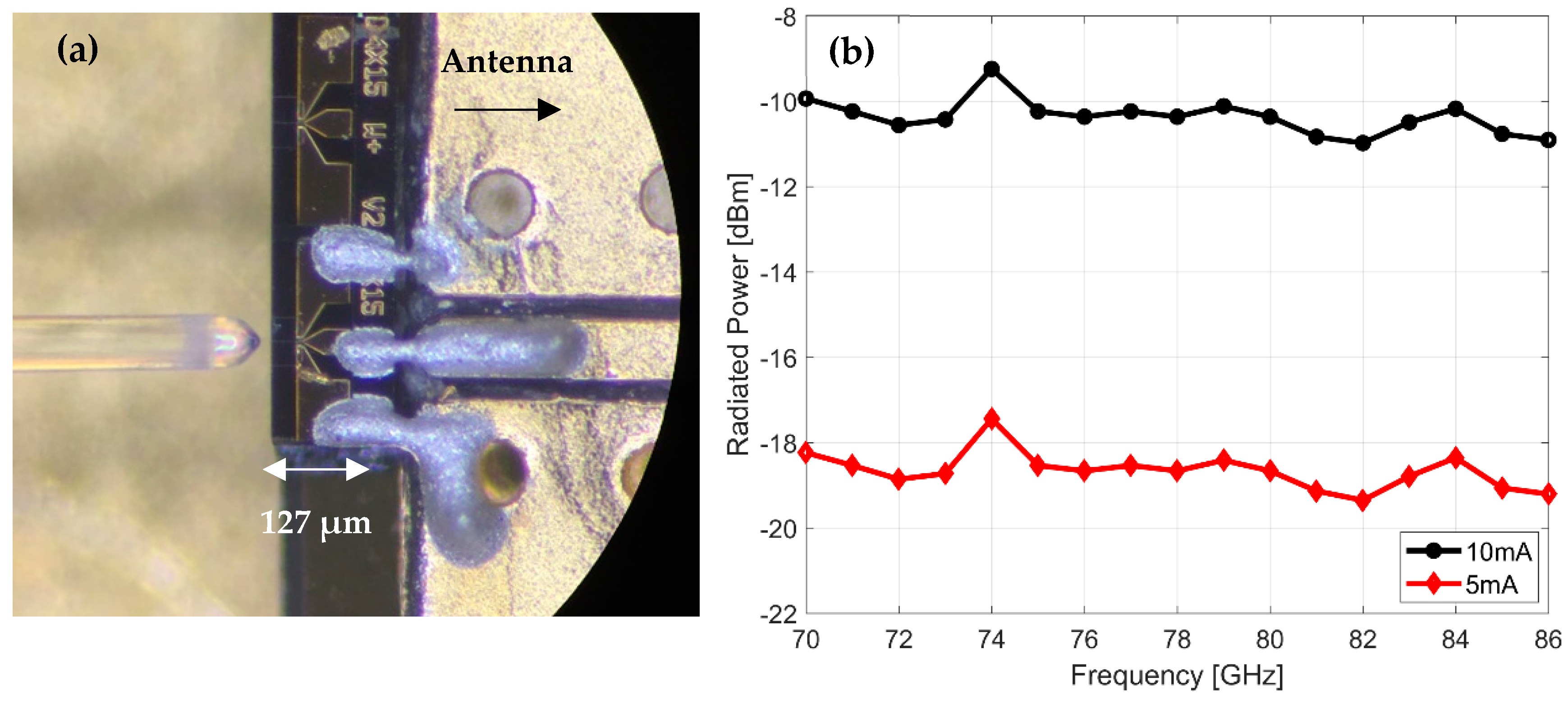
- (a)
- THz communication systems are capable of delivering high-rate data over wireless links, but due to the intrinsic high propagation loss at higher carrier frequencies and the low power generated at these frequencies by photonic sources, the transmission distances achieved so far are typically in the range of about 10 m at 409 GHz [9], and
- (b)
- The electronics-based and photonics-based approaches have been evolving separately, competing with each other, with few efforts to combine both worlds in a truly microwave photonic approach that would benefit from the main key features of each; bandwidth, tunability, stability and fiber compatibility from photonics and power handling capability from the electronics.
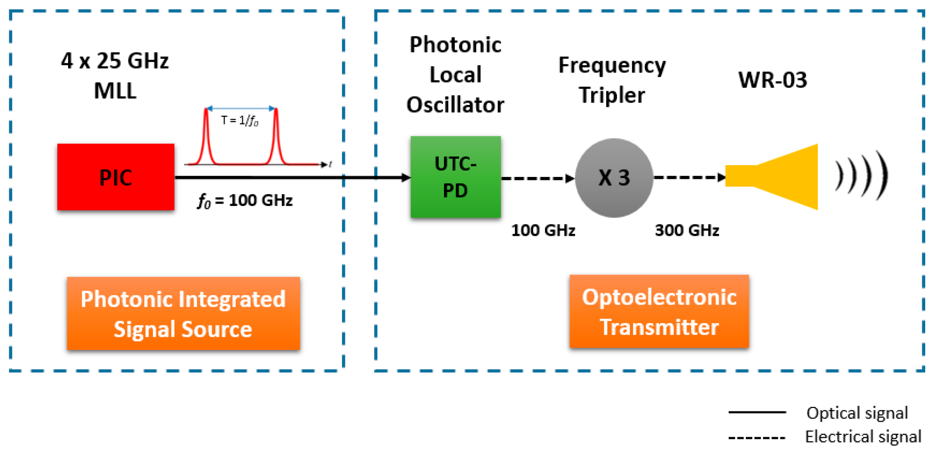
2. 300 GHz Optoelectronic Transmitter
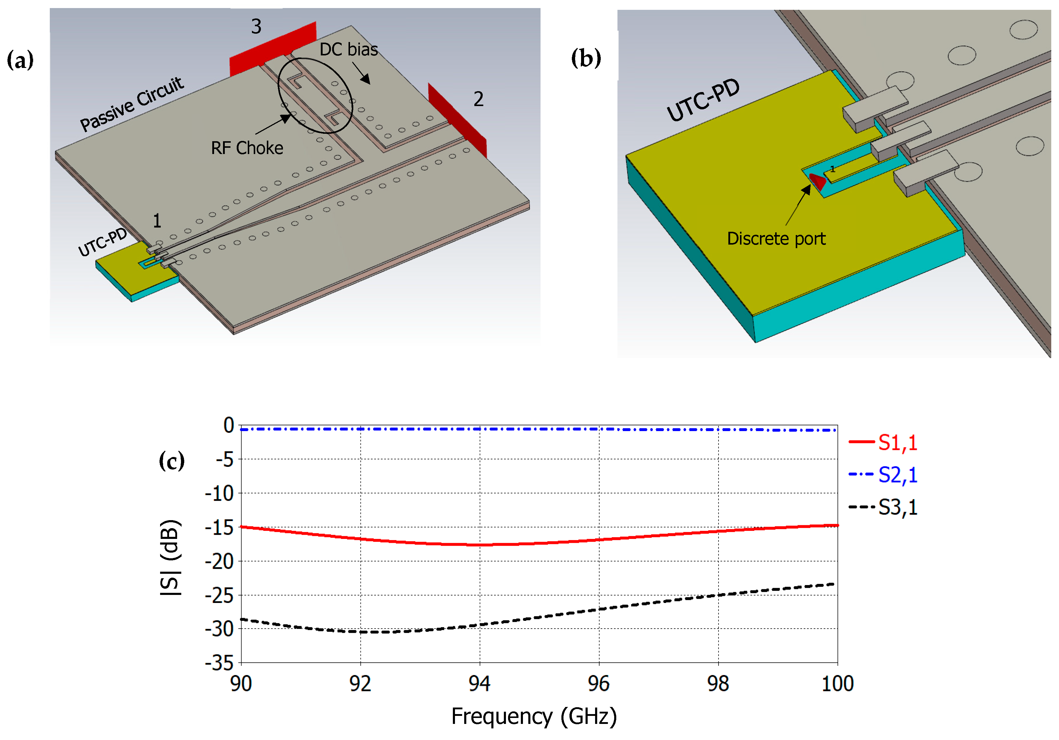
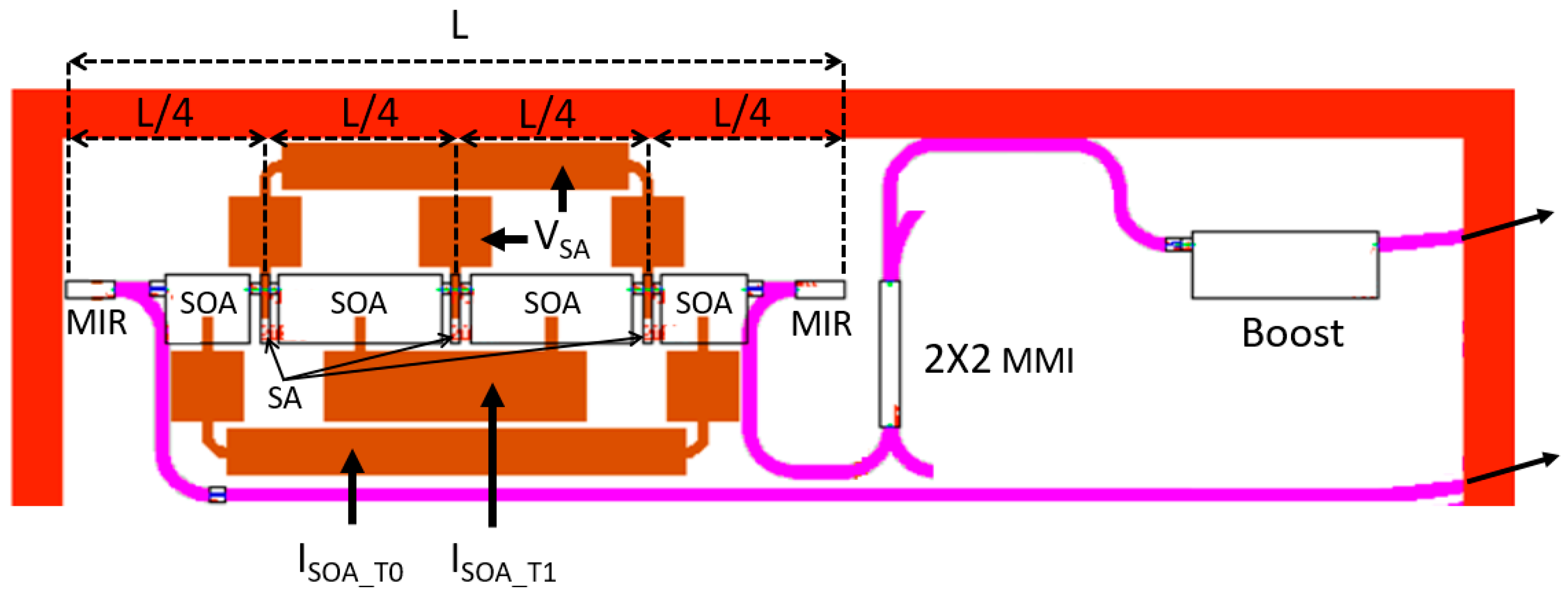
2.1. Photonic Local Oscillator
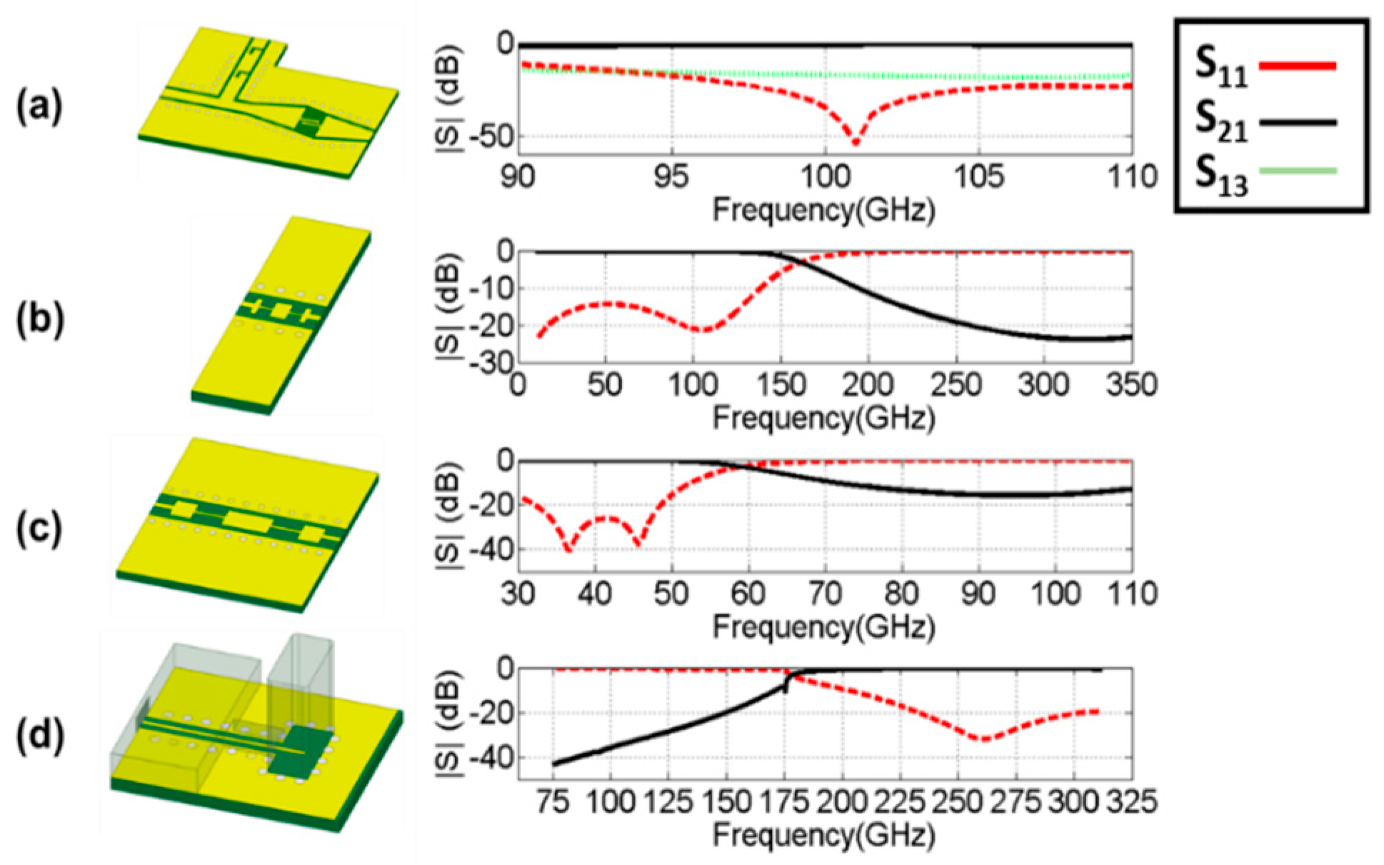
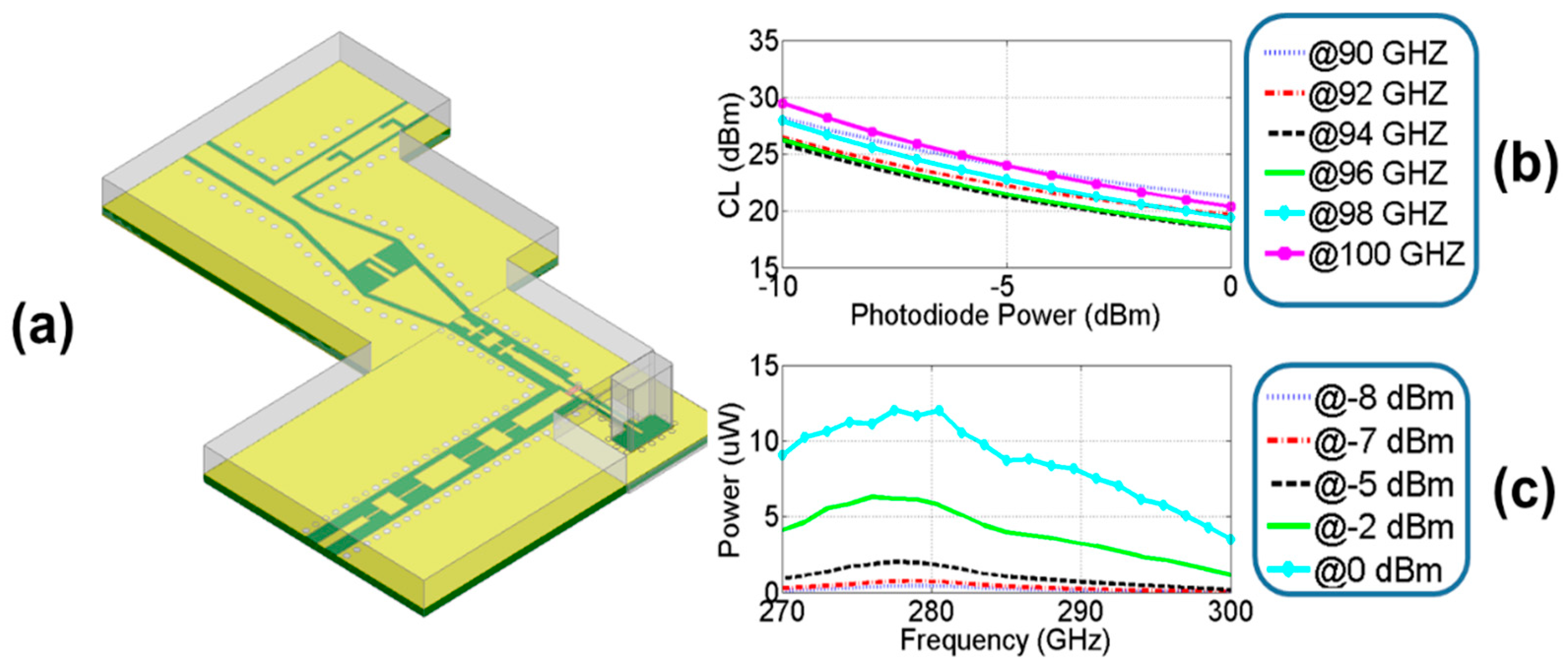
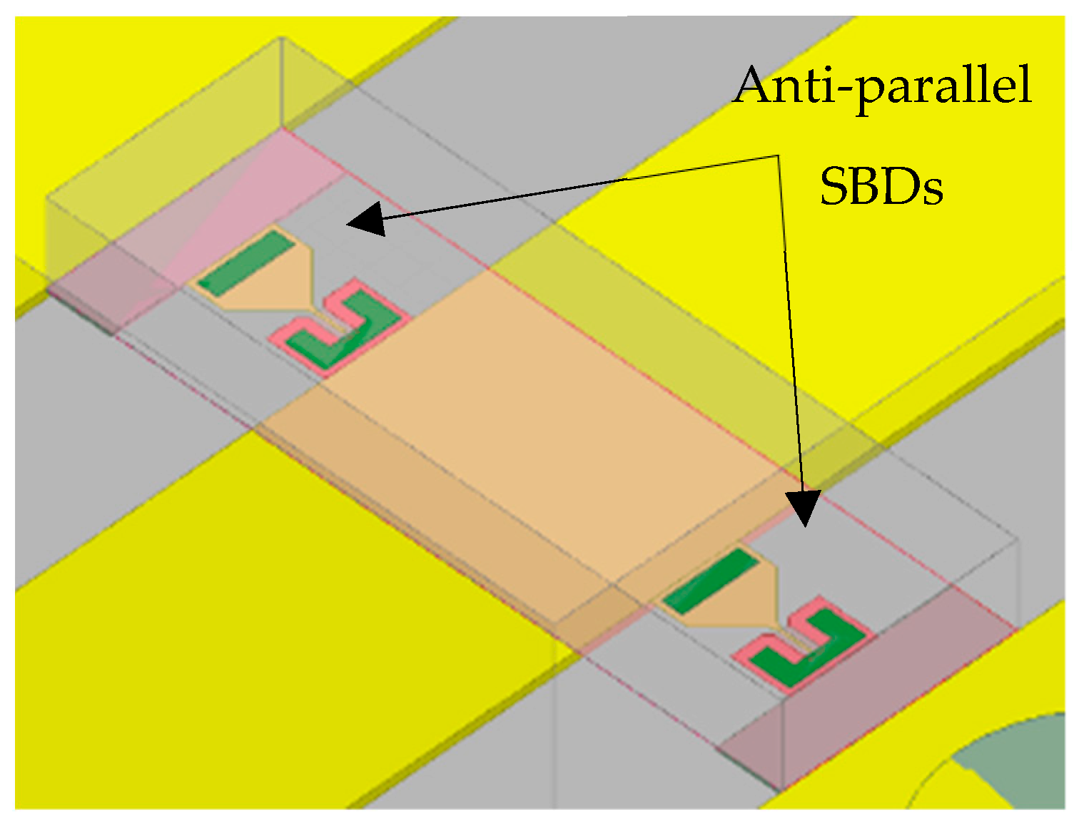
2.2. Frequency Tipler
3. Photonic Integrated Signal Source
3.1. Device Description
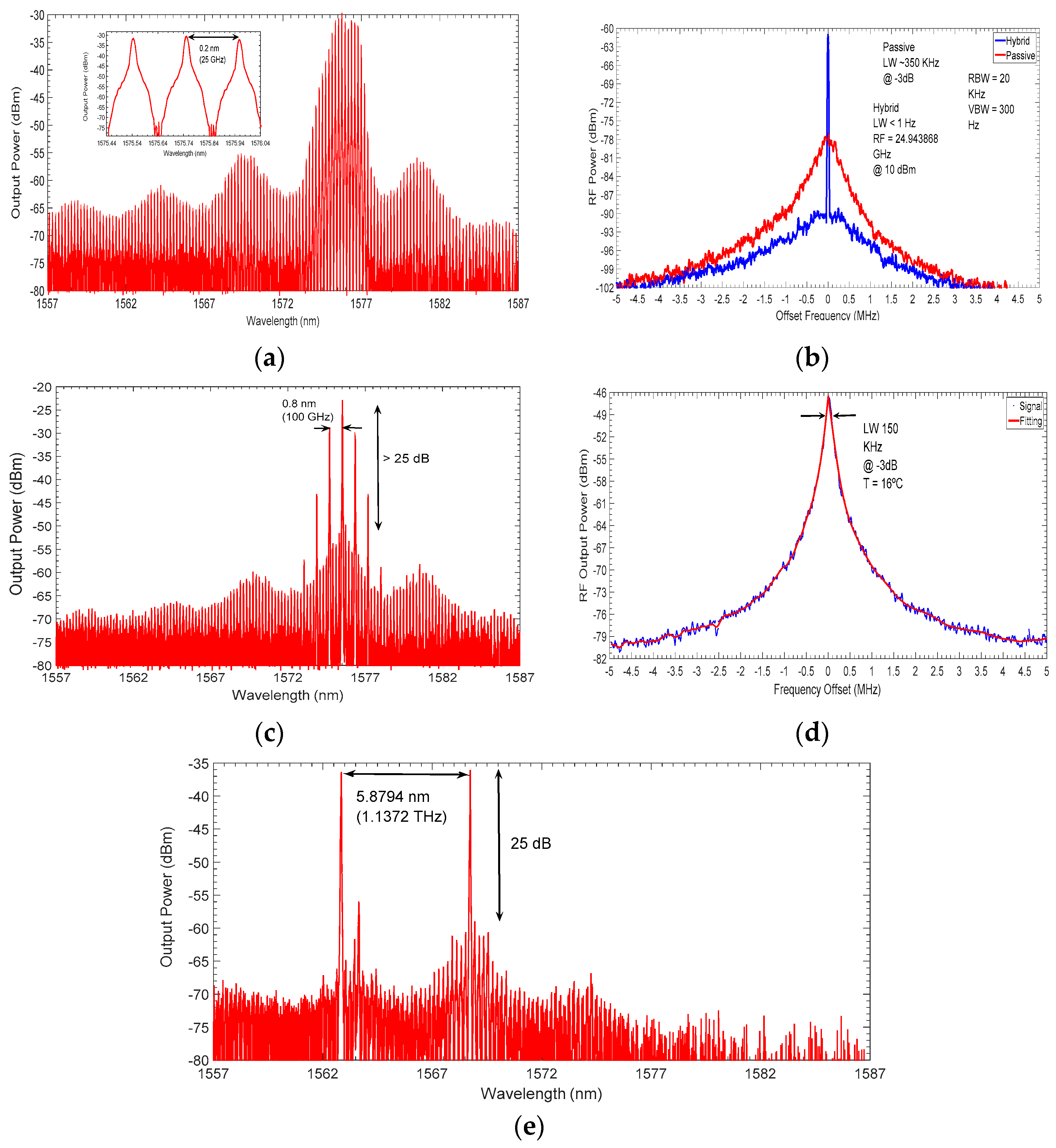
3.2. Characterization Results
4. Conclusions
Author Contributions
Funding
Acknowledgments
Conflicts of Interest
References
- Rappaport, T.S.; Sun, S.; Mayzus, R.; Zhao, H.; Azar, Y.; Wang, K.; Wong, G.N.; Schulz, J.K.; Samimi, M.; Gutierrez, F. Millimeter wave mobile communications for 5G cellular: It will work! IEEE Access 2013, 1, 335–349. [Google Scholar] [CrossRef]
- White Paper, The Zettabyte Era: Trends and Analysis, CISCO. Available online: https://files.ifi.uzh.ch/hilty/t/Literature_by_RQs/RQ%20102/2015_Cisco_Zettabyte_Era.pdf (accessed on 1 January 2019).
- Kürner, T.; Priebe, S. Towards THz communications-status in research, standardization and regulation. J. Infrared Millim. Terahertz Waves 2014, 35, 53–62. [Google Scholar] [CrossRef]
- Kallfass, I.; Antes, J.; Schneider, T.; Kurz, F.; Lopez-Diaz, D.; Diebold, S.; Massler, H.; Leuther, A.; Tessmann, A. All active MMIC-based wireless communication at 220 GHz. IEEE Trans. Terahertz Sci. Technol. 2011, 1, 477–487. [Google Scholar] [CrossRef]
- Chattopadhyay, G. Technology, capabilities, and performance of low power terahertz sources. IEEE Trans. Terahertz Sci. Technol. 2011, 1, 33–53. [Google Scholar] [CrossRef]
- Nagatsuma, T.; Ducournau, G.; Renaud, C.C. Advances in terahertz communications accelerated by photonics. Nat. Photonics 2016, 10, 371. [Google Scholar] [CrossRef]
- Nagatsuma, T.; Horiguchi, S.; Minamikata, Y.; Yoshimizu, Y.; Hisatake, S.; Kuwano, S.; Yoshimoto, N.; Terada, J.; Takahashi, H. Terahertz wireless communications based on photonics technologies. Opt. Express 2013, 21, 23736–23747. [Google Scholar] [CrossRef]
- Shams, H.; Shao, T.; Fice, M.J.; Anandarajah, P.M.; Renaud, C.C.; Van Dijk, F.; Barry, L.P.; Seeds, A.J. 100 Gb/s Multicarrier THz Wireless Transmission System with High Frequency Stability Based on a Gain-Switched Laser Comb Source. IEEE Photonics J. 2015, 3, 1–11. [Google Scholar] [CrossRef]
- Jia, S.; Lo, M.C.; Zhang, L.; Ozolins, O.; Udalcovs, A.; Kong, D.; Pang, X.; Yu, X.; Xiao, S.; Popov, S.; et al. Integrated Dual-DFB Laser for 408 GHz Carrier Generation Enabling 131 Gbit/s Wireless Transmission over 10.7 Meters. In Proceedings of the Optical Fiber Communication Conference (OFC), San Diego, CA, USA, 2–8 March 2019. paper Th1C. [Google Scholar]
- Rouvalis, E.; Chtioui, M.; Tran, M.; Lelarge, F.; van Dijk, F.; Fice, M.J.; Renaud, C.C.; Carpintero, G.; Seeds, A.J. High-speed photodiodes for InP-based photonic integrated circuits. Opt. Express 2012, 20, 9172–9177. [Google Scholar] [CrossRef] [PubMed]
- Chen, Z.; Wang, H.; Alderman, B.; Huggard, P.; Zhang, B.; Fan, Y. 190 GHz high power input frequency doubler based on Schottky diodes and AlN substrate. IEICE Electron. Express 2016, 3, 20160981. [Google Scholar] [CrossRef]
- Song, H.-J.; Ajito, K.; Muramoto, Y.; Wakatsuki, A.; Nagatsuma, T.; Kukutsu, N. Uni-travelling-carrier photodiode module generating 300 GHz power greater than 1 mW. IEEE Microw. Wirel. Compon. Lett. 2012, 22, 363–365. [Google Scholar] [CrossRef]
- Maestrini, A.; Thomas, B.; Wang, H.; Jung, C.; Treuttel, J.; Jin, Y.; Chattopadhyay, G.; Mehdi, I.; Beaudin, G. Schottky diode-based terahertz frequency multipliers and mixers. C. R. Phys. 2010, 11, 480–495. [Google Scholar] [CrossRef]
- Avrutin, E.; Marsh, J.; Portnoi, E. Monolithic and multi-gigahertz mode-locked semiconductor lasers: constructions, experiments, models and applications. IEEE Proc.-Optoelectron. 2000, 147, 251–278. [Google Scholar] [CrossRef]
- Lo, M.-C.; Martínez, R.C.-G.; Carpintero, G. Monolithic mode-locked laser-based optical frequency comb for OFDM integrated on InP generic technology platform. In Proceedings of the Optical Fiber Communication Conference, San Diego, CA, USA, 11–15 March 2018. paper Th1I–1. [Google Scholar]
- Marsh, J.H.; Hou, L. Mode-locked laser diodes and their monolithic integration. IEEE J. Sel. Top. Quantum Electron. 2017, 23, 1–11. [Google Scholar] [CrossRef]
- Chen, Y.K.; Wu, M.C.; Tanbun-Ek, T.; Logan, R.A.; Chin, M.A. Subpicosecond monolithic colliding-pulse mode-locked multiple quantum well lasers. Appl. Phys. Lett. 1991, 58, 1253–1255. [Google Scholar] [CrossRef]
- Avrutin, E.A.; Marsh, J.H.; Arnold, J.M.; Krauss, T.F.; Pottinger, H.; la Rue, R.M.D. Analysis of harmonic (sub) THz passive mode-locking in monolithic compound cavity Fabry-Perot and ring laser diodes. IEE Proc. Optoelectron. 1999, 146, 55–61. [Google Scholar] [CrossRef]
- Arahira, S.; Oshiba, S.; Matsui, Y.; Kunii, T.; Ogawa, Y. Terahertz-rate optical pulse generation from a passively mode-locked semiconductor laser diode. Opt. Lett. 1994, 19, 834–836. [Google Scholar] [CrossRef]
- Katagiri, Y.; Takada, A. A harmonic colliding-pulse mode-locked semiconductor laser for stable subterahertz pulse generation. IEEE Photonics Technol. Lett. 1997, 9, 1442–1444. [Google Scholar] [CrossRef]
- Martins-Filho, J.F.; Avrutin, E.A.; Ironside, C.N.; Roberts, J.S. Monolithic multiple colliding pulse mode-locked quantum-well lasers, experiment and theory. IEEE J. Sel. Top. Quantum Electron. 1995, 1, 539–551. [Google Scholar] [CrossRef]
- Kleijn, E.; Smit, M.K.; Leijtens, X.J. Multimode interference reflectors: A new class of components for photonic integrated circuits. J. Light. Technol. 2013, 31, 3055–3063. [Google Scholar] [CrossRef]
- Stopinski, S.; Malinowski, M.; Piramidowicz, R.; Kazmierski, C.; Smit, M.K.; Leijtens, X.J. Photonic integrated multichannel wdm modulators for data read-out units. J. Light. Technol. 2014, 3879–3887. [Google Scholar] [CrossRef]
- Morrissey, P.E.; Kelly, N.; Dernaika, M.; Caro, L.; Yang, H.; Peters, F.H. Coupled cavity single-mode laser based on regrowth-free integrated MMI reflectors. IEEE Photonics Technol. Lett. 2016, 28, 1313–1316. [Google Scholar] [CrossRef]
- Lo, M.-C.; Guzmán, R.; Gordón, C.; Carpintero, G. Mode-locked laser with pulse interleavers in a monolithic photonic integrated circuit for millimeter wave and terahertz carrier generation. Opt. Lett. 2017, 42, 1532–1535. [Google Scholar] [CrossRef] [PubMed]


© 2019 by the authors. Licensee MDPI, Basel, Switzerland. This article is an open access article distributed under the terms and conditions of the Creative Commons Attribution (CC BY) license (http://creativecommons.org/licenses/by/4.0/).
Share and Cite
Ali, M.; Pérez-Escudero, J.M.; Guzmán-Martínez, R.-C.; Lo, M.-C.; Ederra, I.; Gonzalo, R.; García-Muñoz, L.E.; Santamaría, G.; Segovia-Vargas, D.; van Dijk, F.; et al. 300 GHz Optoelectronic Transmitter Combining Integrated Photonics and Electronic Multipliers for Wireless Communication. Photonics 2019, 6, 35. https://doi.org/10.3390/photonics6020035
Ali M, Pérez-Escudero JM, Guzmán-Martínez R-C, Lo M-C, Ederra I, Gonzalo R, García-Muñoz LE, Santamaría G, Segovia-Vargas D, van Dijk F, et al. 300 GHz Optoelectronic Transmitter Combining Integrated Photonics and Electronic Multipliers for Wireless Communication. Photonics. 2019; 6(2):35. https://doi.org/10.3390/photonics6020035
Chicago/Turabian StyleAli, Muhsin, Jose Manuel Pérez-Escudero, Robinson-Cruzoe Guzmán-Martínez, Mu-Chieh Lo, Iñigo Ederra, Ramón Gonzalo, Luis Enrique García-Muñoz, Gabriel Santamaría, Daniel Segovia-Vargas, Frédéric van Dijk, and et al. 2019. "300 GHz Optoelectronic Transmitter Combining Integrated Photonics and Electronic Multipliers for Wireless Communication" Photonics 6, no. 2: 35. https://doi.org/10.3390/photonics6020035
APA StyleAli, M., Pérez-Escudero, J. M., Guzmán-Martínez, R.-C., Lo, M.-C., Ederra, I., Gonzalo, R., García-Muñoz, L. E., Santamaría, G., Segovia-Vargas, D., van Dijk, F., & Carpintero, G. (2019). 300 GHz Optoelectronic Transmitter Combining Integrated Photonics and Electronic Multipliers for Wireless Communication. Photonics, 6(2), 35. https://doi.org/10.3390/photonics6020035