Article

Enhanced Crystal Quality of AlxIn1-xAsySb1-y for Terahertz Quantum Cascade Lasers

1
TU Wien, Institude of Solid State Electronics, Floragasse 7, 1040 Wien, Austria
2
Austrian Academy of Sciences, Dr. Ignaz Seipel-Platz 2, 1010 Wien, Austria
3
TU Wien, Center for Micro and Nano Structures, Floragasse 7, 1040 Wien, Austria
*
Author to whom correspondence should be addressed.
Photonics 2016, 3(2), 20; https://doi.org/10.3390/photonics3020020
Submission received: 31 March 2016 / Revised: 14 April 2016 / Accepted: 15 April 2016 / Published: 20 April 2016
(This article belongs to the Special Issue Quantum Cascade Lasers - Advances and New Applications)

Abstract

:
This work provides a detailed study on the growth of AlxIn1-xAsySb1-y lattice-matched to InAs by Molecular Beam Epitaxy. In order to find the conditions which lead to high crystal quality deep within the miscibility gap, AlxIn1-xAsySb1-y with x = 0.462 was grown at different growth temperatures as well as As2 and Sb2 beam equivalent pressures. The crystal quality of the grown layers was examined by high-resolution X-ray diffraction and atomic force microscopy. It was found that the incorporation of Sb into Al0.462In0.538AsySb1-y is strongly temperature-dependent and reduced growth temperatures are necessary in order to achieve significant Sb mole fractions in the grown layers. At 480 C lattice matching to InAs could not be achieved. At 410 C lattice matching was possible and high quality films of Al0.462In0.538AsySb1-y were obtained.

1. Introduction

InAs is an interesting material for inter-subband devices such as quantum cascade lasers (QCLs) due to its low effective mass, since it is expected to enable higher performance by providing higher gain [1]. In order to exploit the beneficial properties of InAs as the well material, a suitable barrier material is necessary. The commonly used Al(As)Sb material, though enabling excellent results for mid-infrared (MIR) devices [2,3,4,5], requires the use of monolayer and sub-monolayer thin barriers for devices designed to emit in the terahertz ( T Hz ) regime, due to its very high conduction band offset. The growth of such thin layers is very difficult to control, and to date, no THz laser operation has been shown.
A viable option for the barrier material is the quarternary AlxIn1-xAsySb1-y material, which can be grown lattice-matched to InAs and should have properties tunable from InAs to AlAs0.16Sb0.84. By choosing an appropriate composition, it would be possible to grow InAs based THz QCLs with a low conduction band offset and therefore easy to control barrier thicknesses.
Reports about the growth of AlxIn1-xAsySb1-y at various compositions can be found in literature, however, most of these works do not specifically study the growth of AlxIn1-xAsySb1-y and hence little information exists on the effect of the various growth parameters on the crystal quality and layer composition. An overview of the compositions and the respective growth temperatures is given in Figure 1. Turner et al. [6] and Wilk et al. [7] report on the growth AlxIn1-xAsySb1-y with Al mole fractions below 0.20 at growth temperatures (Tg) of 430 C and 420 C , while Semenov et al. [8] show that compositions with Al mole fractions of up to 0.25 can be grown at a Tg of 450°C to 500 C . For the greatest flexibility when it comes to designing devices employing AlxIn1-xAsySb1-y, composition with higher Al mole fractions have to be investigated and conditions have to be found which suit the widest range of compositions. The growth of AlxIn1-xAsySb1-y on GaAs with higher Al mole fractions is reported at a Tg well below 400 C . Kudo et al. [9] studied the incorporation of Sb into AlxIn1-xAsySb1-y with an Al mole fraction of 0.5 at a Tg of 350 C grown on GaAs. The authors report a high dislocation density, found in a transmission electron microscopy study of the grown material, resulting from the highly lattice-mismatched conditions. It is questionable whether this result is applicable to the growth of AlxIn1-xAsySb1-y on InAs. Wahsington-Stokes et al. [10] report on the growth of AlxIn1-xAsySb1-y with an As mole fraction between 0.37 and 0.72 at a Tg between 355°C and 378 C on GaSb substrates and report good crystal quality for the grown layers. The influence of the Sb and As beam equivalent pressures (BEP) or the Tg on the quality and composition of the layers is not mentioned.

2. Experiment Section

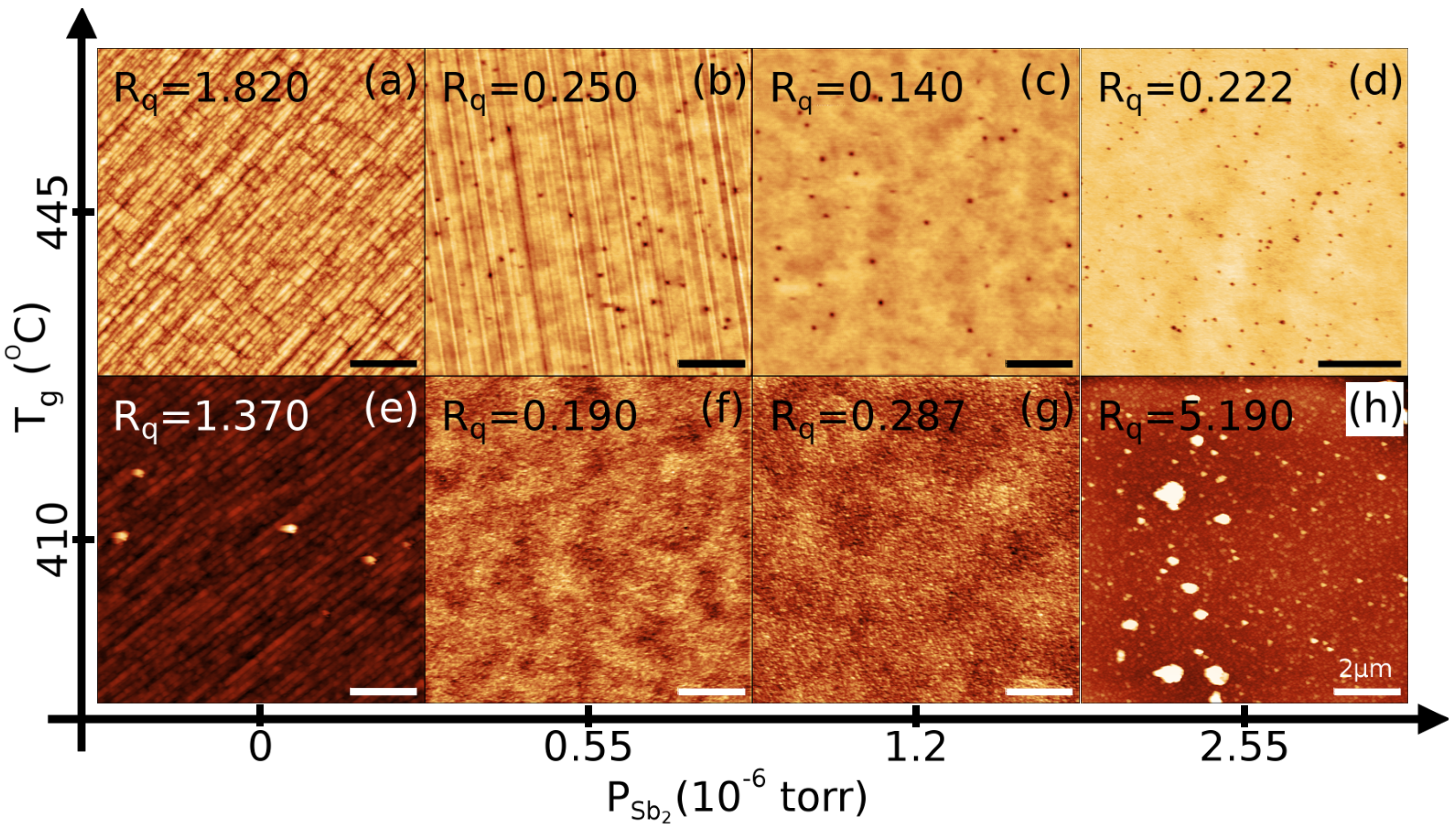
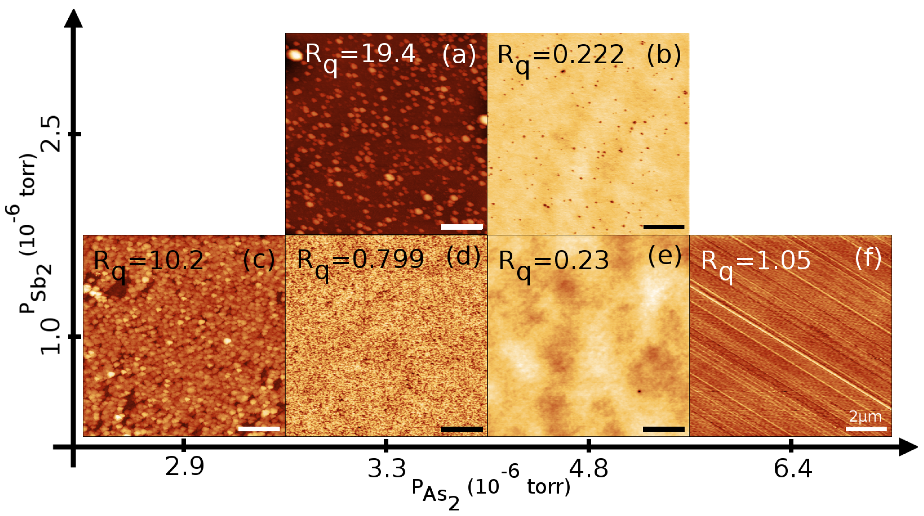
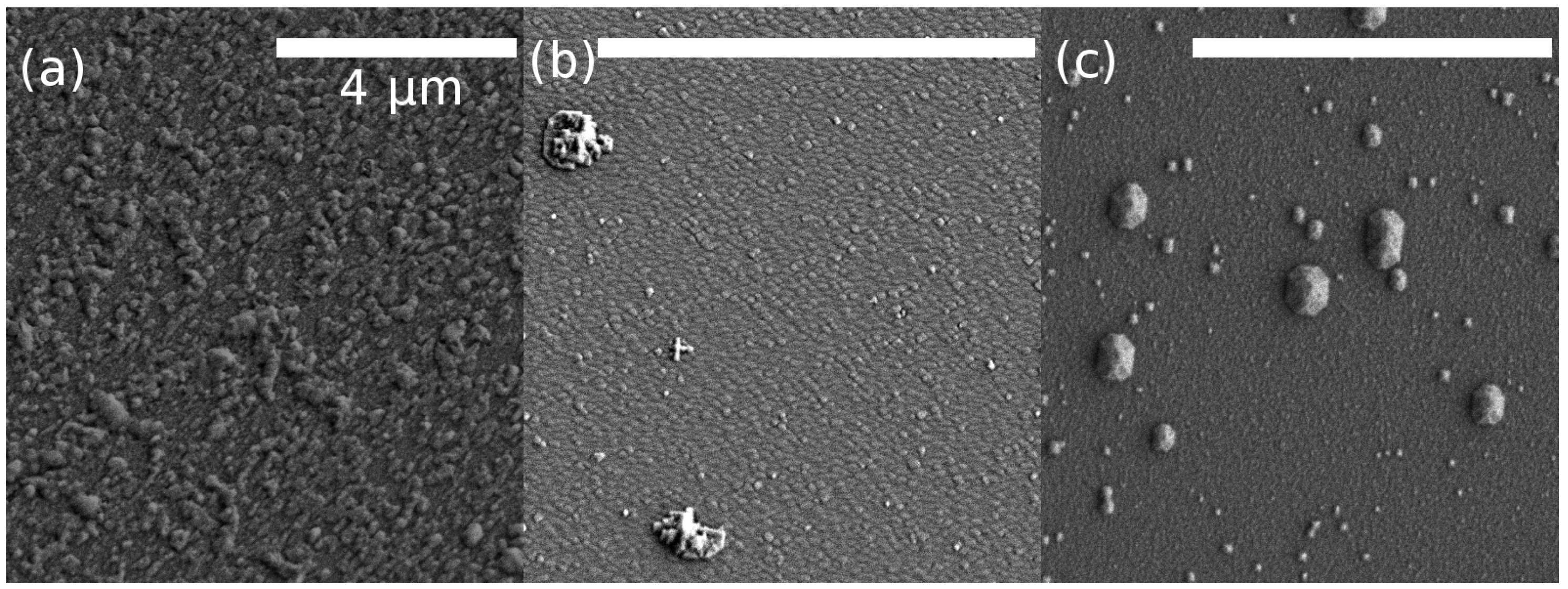
2.1. Growth Optimization of AlxIn1-xAsySb1-y

The lack of information on the growth of AlxIn1-xAsySb1-y with Al mole fractions around 0.5 at a Tg above 400 C suggests that challenges, possible due to the presence of a miscibility gap [8], arise from such conditions. Since high crystal quality is expected to be achieved at high Tg, the upper limit for the growth of AlxIn1-xAsySb1-y and the dependence of the crystal quality on the Tg have to be investigated.
AlxIn1-xAsySb1-y with an aluminum mole fraction fixed to 0.462, was grown on InAs. The growth rates of AlAs (on InAs) (RAlAs) and InAs (RInAs) were constant for all samples. RAlAs was set to 0.25 monolayers per second (MLs−1) which corresponds to an aluminum BEP 1.3 × 10⁻⁷ torr . RInAs was set to 0.29 MLs−1 equaling an indium BEP of 4.5 × 10⁻⁷ torr . For the comparison of the group V BEPs to other MBE systems, the As2 flux was calibrated by the (2 × 4) to (4 × 2) transition during growth at different temperatures and normalized to 1 MLs−1. A fit to the exponential function P As 2 ( T ) = a + b exp ( T c ) resulted in the parameters a = 0 . 531 torr , b = 2 . 14 × 10 - 14 torr , c = 23 . 24 K - 1 . A plot of this experiment can be found in the supplementary material section.
To find the optimum growth conditions, Tg, As2 BEP (PAs2) and Sb2 BEP (PSb2) were varied. The range of Tg used in this study was 410°C to 480 C . Since AlxIn1-xAsySb1-y should be used in heterostructures together with InAs, PAs2 is, in principle, dictated by the optimum BEP to grow high quality InAs [11]. In this study, PAs2 was varied in order to investigate its influence on the composition of Al0.462In0.538AsySb1-y. The growth parameter regions investigated in this study are indicated by the gray shaded areas in Figure 1.
To investigate the influence of growth parameters, a set of samples was grown in a Riber 32 MBE system on indium-bonded n+ InAs (001) wafers. For the group V materials, valved cracking cells were used with the cracking zone temperatures set to 850°C and 1000 C to produce As2 and Sb2 respectively. For all samples, first the oxide was thermally desorbed under PAs2 of 1.5 × 10⁻⁵ torr at 510 C for 20 min. The temperature was then reduced to 480 C to grow a 150 n m InAs buffer layer to enhance the surface quality after thermal desorption of the oxide. Next, the Tg was adjusted to the desired growth temperature, at which a 150 n m thick Al0.462In0.538AsySb1-y layer and a 5 n m InAs cap, were grown.
All fabricated heterostructures were measured with high resolution x-ray diffraction (HRXRD) to investigate the crystal quality and composition. The As mole fraction (y) in the grown Al0.462In0.538AsySb1-y layers was corroborated by measuring their in-plane and out-of-plane lattice constant in reciprocal space maps around the InAs (224) diffraction peak and applying Vegard’s law. Atomic force microscopy (AFM) was used to determine the surface roughness of all samples.
To investigate the incorporation of Sb into Al0.462In0.538AsySb1-y, three series of samples were grown. For each series PAs2 and the Tg were kept constant while PSb2 was varied. PAs2 was chosen such that high crystal quality InAs can be grown under the same conditions [11]. The results are summarized in Figure 2a. It shows that with increasing PSb2, the rate of Sb incorporation is lowered and a maximum achievable Sb mole fraction is approached asymptotically. Only at a Tg of 410 C can lattice matching with InAs achieved. An explanation for this behavior may be found in the As-for-Sb exchange reaction found for other mixed group V materials like GaAsSb [14]. Due to its negative enthalpy, this reaction is favored with respect to the reverse reaction and its rate rises with Tg for experiments using As2, which is in agreement with our observations.
HRXRD measurements, shown in Figure 2b–d, show high crystal quality for PSb2 between 0.5 × 10⁻⁶ torr and 1 × 10⁻⁶ torr at 410 C as well as 1 × 10⁻⁶ torr and 2.5 × 10⁻⁶ torr at 445 C Tg. This is indicated by sharp layer peaks and Pendellösung fringes. At lower PSb2, the layer peaks are broadened due to partial relaxation resulting from the high lattice mismatch. At 410 C , even higher PSb2 also leads to peak broadening. The respective (224) reciprocal space map shows partial relaxation. Strong peak broadening due to partial relaxation was also found for all samples grown at 480 C .
AFM measurements performed on the same heterostructures, shown in Figure 3, confirm these observations. Layers containing very little Sb show crosshatch patterns, a sign of partial relaxation. When the PSb2 is increased to values between 0.5 × 10⁻⁶ torr and 1 × 10⁻⁶ torr for a Tg of 410 C and 1 × 10⁻⁶ torr and 2.5 × 10⁻⁶ torr at 445 C , the surface roughness is dramatically reduced and no sign of crosshatch can be found. At 2.55 × 10⁻⁶ torr and a Tg of 410 C , the measurements show an increased surface roughness. Since these conditions cause a 3-D growth mode it is evident that excess Sb2 has to be avoided at low Tg in order to achieve high crystal quality.
Although it is convenient to keep PAs2 at a value that is optimal for the growth of the InAs throughout the whole growth, it is possible to change the conditions for each layer, since modern As cracking cells are equipped with valves that allow for the quick change of the flux. It could be beneficial to change PAs2 to a lower value for the growth of AlxIn1-xAsySb1-y in order to achieve a lower As mole fraction in the layer and hereby circumvent the restrictions imposed by the growth of InAs. To investigate the influence of PAs2 on the composition of Al0.462In0.538AsySb1-y, a series of samples was grown in which PSb2 (1 × 10⁻⁶ torr and 2.5 × 10⁻⁶ torr ) and the growth temperature (Tg = 445 C ) were kept constant while PAs2 was varied. AFM measurements of these samples are shown in Figure 4. From Figure 5a it can be seen that, as expected, decreasing PAs2 leads to a lower As concentration (y) in the layer. Figure 5b, shows that the PAs2 can only be adjusted within a very small range since too little As2 leads to a dramatic increase in surface roughness, due a 3-D growth mode (Figure 4c). This behavior is even more pronounced for samples grown at PSb2 of 2.5 × 10⁻⁶ torr (Figure 4a). When PAs2 is decreased below ∼3 × 10⁻⁶ torr no epitaxial growth is possible, illustrating that there is a lower limit to the PAs2. This was determined by both a vanishing RHEED pattern during growth and the absence of a layer peak in the HRXRD measurement.
To understand its origin, samples showing high roughness but no cross hatch in the AFM analysis have been inspected by scanning electron microscopy (SEM) and energy dispersive X-ray spectroscopy (EDX). The micrographs of these samples are shown in Figure 6. Figure 6a shows the effect of low PAs2 on the surface morphology. The too low As flux on the surface leads to a lower surface mobility of the group III adatoms, breaking the layer-by-layer growth mode and resulting in a rough surface. EDX measurements at different spots of the sample show that the four atom species (Al,In,As,Sb) are equally distributed ( σ < 0 . 5 at . % ). Figure 6b shows the effect of high PSb2 at low Tg. Similar to Figure 6a 3-D growth was found. Since this sample was grown with excess PAs2, group V deficiency can be ruled out as the source. As for the previous sample, the EDX analysis showed that all four atom species are homogeneously distributed ( σ < 0 . 5 at . % ). Increasing PSb2 well beyond lattice-matching seems to limit the diffusion length of the group III elements and promote a 3-D growth mode. For both sample (a) and (b) no signs of phase separation due to immiscibility were found and the 3-D morphology seems to be caused by the III/V BEP ratios. High surface roughness was also found for the sample shown in Figure 6c. Unlike for samples (a) and (b) it seems to be due to crystallites with an octagonal base that are well ordered to the substrate. The EDX measurement on this sample shows that the crystallites are rich in antimony while in the surrounding area the composition is close to that found in the HRXRD study. Al and In are homogeneously distributed across the whole sample. This result suggests that Al0.462In0.538AsySb1-y decomposes into AlInAs and AlInSb under these conditions.
Using the information gathered in this study, two samples were grown on a Riber C21 MBE system on freestanding n+ InAs (001) wafers at a Tg of 410 C . Al mole fractions of 0.25 and 0.53 were chosen and the As2 BEP was adjusted for high quality InAs. PSb2 was then adjusted in order to achieve lattice matching with InAs. For both compositions high-quality material was obtained, again confirmed by HRXRD and AFM measurements.

2.2. Low Temperature Growth of InAs Based Inter-Subband Devices

The experimental data presented in this work show that low Tg is necessary in order to achieve high crystal quality for both, InAs and Al0.462In0.538AsySb1-y. Growth performed at very low Tg, however, can lead to low device performance due to a deterioration of the optical properties and interface quality of the grown materials. To ensure that the requirement to grow at low Tg does not prevent the realization of inter-subband devices, InAs-based devices using AlAsSb barriers were designed and grown at a Tg of 400 C . A quantum cascade detector (QCD) structure with a vertical transition was designed using a semi-classical Monte-Carlo approach. The device was processed into a mesa structure and illuminated through a 45° wedge faced. It showed a peak specific detectivity 2.7 × 10⁷ c m Hz / W at 300 K and a center detection wavelength of 4.84 μ m [15]. Moreover, a THz QCL structure based on a 3-well resonant phonon depletion design was grown. Lasing emission at 3.8 T Hz was observed by applying a magnetic field at liquid helium temperature. This is the first report of laser performance in the THz regime for InAs-based structures [16].

3. Discussions

A summary of all samples used in this study that have been grown at Tg = 445 C (a) and 410 C (b) is given in Figure 7. In both cases, a large PAs2/PSb2 ratio leads to cross hatch, due to a large lattice mismatch. For a Tg of 445 C , a PAs2 below 3.3 × 10⁻⁶ torr leads to a rough surface. Roughening was also found for samples grown at a Tg of 410 C for the highest PSb2 of 2.5 × 10⁻⁶ torr . While partial relaxation was found in the reciprocal space map around the InAs (224), the roughening seems to be mainly caused by the high PSb2 since no sign of cross hatch was found in either EDX or AFM measurements. Growing at higher PSb2 at a Tg of 445 C results in lower film quality, due to the formation of ordered crystallites with an octagonal base. Since these crystallites were found to be rich in Sb in the EDX analysis, it appears that decomposition, probably due to the miscibility gap of the material occurs under these conditions. A first order approximation, shown as the gray shaded area in Figure 7, was used to locate the region of pressures for which lattice matching can be expected. At a Tg of 445 C this region is close, if not within, the region which leads to decomposition and the formation of Sb rich crystallites. At a Tg of 410 C the region at which lattice matching is expected is far below the region for which the roughening due to high PSb2 is observed and the growth of lattice-matched high quality material is easily achieved.
The data presented in this study suggests that a Tg of 445 C is the upper limit for lattice matched growth of Al0.462In0.538AsySb1-y. For a stable growth and high quality material, however, it is advised to use even lower Tg. This is even more critical if the conditions for high-quality InAs and Al0.462In0.538AsySb1-y have to be met simultaneously.

4. Conclusions

We investigated the growth of Al0.462In0.538AsySb1-y. It was shown that the incorporation of Sb into Al0.462In0.538AsySb1-y is strongly temperature-dependent and that this is determining the upper limit of the Tg for which lattice matching can be achieved. Moreover, it was found that the quality of the grown material is very sensitive to the used PAs2, and that low pressures, which are necessary to achieve lattice matching, dramatically increase the roughness of the grown layer. Moreover, it was found that the growth of compositions close to lattice matching at a Tg of 445 C leads to decomposition of AlxIn1-xAsySb1-y into AlInAs and AlInSb and the formation of crystallites which significantly decrease in crystal quality. Below this limit, the requirements for the growth of high quality Al0.462In0.538AsySb1-y and lattice matched growth can be met simultaneously. At a growth temperature of 410 C , high quality Al0.462In0.538AsySb1-y layers, confirmed by both HRXRD and AFM measurements, were grown. To ensure that growth at low Tg does not prevent the use of this material for inter-subband devices, two InAs based inter-subband structures, a QCD and a THz-QCL, were grown. The QCD showed a peak specific detectivity 2.7 × 10⁷ c m Hz / W at 300 K at a center detection wavelength of 4.84 μ m . For the THz-QCL, we were able to show the first lasing emission in the THz regime, at an emission frequency of 3.8 T Hz , for InAs-based structures.

Supplementary Files

Supplementary File 1

Acknowledgments

The authors acknowledge funding by the Austrian Science Fund (FWF): F4909-N23 (NextLite), W1243 (Solids4Fun), F2503-N17 (IRON), as well as support by the Austrian Society for Micro- and Nanoelectronics (GMe). H.D. is an APART fellow of the Austrian Academy of Sciences.

Author Contributions

T.Z. conceived and designed the experiments, performed HRXRD, SEM, EDX and AFM measurements and analyzed the data; T.Z. and A.M.A. grew samples and wrote the paper; D.M., H.D. and W.S. configured the MBE for the growth of AlxIn1-xAsySb1-y; G.S. supervised the study. All authors contributed to scientific discussions and commented on the manuscript.

Conflicts of Interest

The authors declare no conflict of interest.

References

  1. Ohtani, K.; Ohno, H. InAs/AlSb quantum cascade lasers operating at 10 μm. Appl. Phys. Lett. 2003, 82, 1003–1005. [Google Scholar] [CrossRef]
  2. Teissier, R.; Barate, D.; Vicet, A.; Alibert, C.; Baranov, A.; Marcadet, X.; Renard, C.; Garcia, M.; Sirtori, C.; Revin, D.; Cockburn, J. Room temperature operation of InAs/AlSb quantum cascade lasers. Appl. Phys. Lett. 2004, 85, 167–169. [Google Scholar] [CrossRef]
  3. Devenson, J.; Teissier, R.; Cathabard, O.; Baranov, A. InAs/AlSb quantum cascade lasers emitting below 3 μm. Appl. Phys. Lett. 2007, 90. [Google Scholar] [CrossRef]
  4. Devenson, J.; Cathabard, O.; Teissier, R.; Baranov, A. InAsAlSb quantum cascade lasers emitting at 2.75–2.97 μm. Appl. Phys. Lett. 2007, 91. [Google Scholar] [CrossRef]
  5. Marcadet, X.; Renard, C.; Carras, M.; Garcia, M.; Massies, J. InAs/AlAsSb based quantum cascade lasers. Appl. Phys. Lett. 2007. [Google Scholar] [CrossRef]
  6. Turner, G.W.; Choi, H.K.; Le, H.Q. Growth of InAsSb quantum wells for long-wavelength (∼4 μm) lasers. J. Vac. Sci. Technol. B Microelectron. Nanometer Struct. 1995, 13, 699. [Google Scholar] [CrossRef]
  7. Wilk, A.; Fraisse, B.; Christol, P.; Boissier, G.; Grech, P.; El Gazouli, M.; Rouillard, Y.; Baranov, A.; Joullié, A. MBE growth of InAs/InAsSb/InAlAsSb “W” quantum well laser diodes emitting near 3 μm. J. Cryst. Growth 2001, 227–228, 586–590. [Google Scholar] [CrossRef]
  8. Semenov, A.; Solov’ev, V.; Meltser, B.; Terent’ev, Y.; Prokopova, L.; Ivanov, S. Molecular beam epitaxy of AlInAsSb alloys near the miscibility gap boundary. J. Cryst. Growth 2005, 278, 203–208. [Google Scholar] [CrossRef]
  9. Kudo, M.; Mishima, T. MBE growth of Si-doped InAlAsSb layers lattice-matched with InAs. J. Cryst. Growth 1997, 175–176, 844–848. [Google Scholar] [CrossRef]
  10. Washington-Stokes, D.; Hogan, T.; Chow, P.; Golding, T.; Kirschbaum, U.; Littler, C.; Lukic, R. AlxIn1-xAs1-ySby/GaSb effective mass superlattices grown by molecular beam epitaxy. J. Cryst. Growth 1999, 201–202, 854–857. [Google Scholar] [CrossRef]
  11. Ye, H.; Li, L.; Hinkey, R.; Yang, R.; Mishima, T.; Keay, J.; Santos, M.; Johnson, M. MBE growth optimization of InAs (001) homoepitaxy. J. Vac. Sci. Technol. B Nanotechnol. Microelectron. 2013, 31. [Google Scholar] [CrossRef]
  12. Rojas-Ramirez, J.; Wang, S.; Contreras-Guerrero, R.; Caro, M.; Bhatnagar, K.; Holland, M.; Oxland, R.; Doornbos, G.; Passlack, M.; Diaz, C.; et al. AlxIn1-xAsySb1-y alloys lattice matched to InAs(100) grown by molecular beam epitaxy. J. Cryst. Growth 2015, 425, 33–38. [Google Scholar] [CrossRef]
  13. Sarney, W.; Svensson, S.; Wang, D.; Donetsky, D.; Kipshidze, G.; Shterengas, L.; Lin, Y.; Belenky, G. AlInAsSb for M-LWIR detectors. J. Cryst. Growth 2015, 425, 357–359. [Google Scholar] [CrossRef]
  14. Losurdo, M.; Capezzuto, P.; Bruno, G.; Brown, A.S.; Brown, T.; May, G. Fundamental reactions controlling anion exchange during mixed anion heterojunction formation: Chemistry of As-for-Sb and Sb-for-As exchange reactions. J. Appl. Phys. 2006, 100. [Google Scholar] [CrossRef]
  15. Reininger, P.; Zederbauer, T.; Schwarz, B.; Detz, H.; MacFarland, D.; Andrews, A.M.; Schrenk, W.; Strasser, G. InAs/AlAsSb based quantum cascade detector. Appl. Phys. Lett. 2015, 107. [Google Scholar] [CrossRef]
  16. Brandstetter, M.; Kainz, A.M.; Zederbauer, T.; Krall, M.; Schönhuber, S.; Detz, H.; Schrenk, W.; Andrews, A.M.; Strasser, G.; Unterrainer, K. InAs based terahertz quantum cascade lasers. Appl. Phys. Lett. 2016, 108. [Google Scholar] [CrossRef]
Figure 1. Reports on the growth of AlxIn1-xAsySb1-y found in literature. (a) Compositions and (b) their respective Tg. The dashed lines in (a) indicate the compositions of AlxIn1-xAsySb1-y which are lattice matched to InAs or GaSb according to Vegard’s Law. ( Photonics 03 00020 i001 
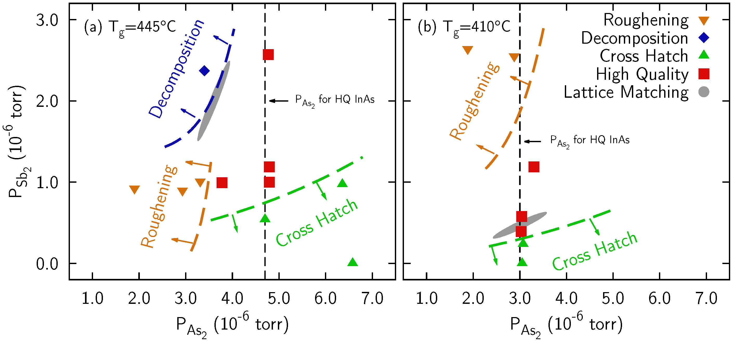
condition explicitly mentioned; the range studied is indicated by the outlined areas) Semenov et al. [8] grown on InAs; similar results were obtained by Rojas-Ramirez et al. [12]; ( ) Washington-Stokes et al. [10] grown on GaSb; ( ) Turner et al. [6] grown on GaSb; ( ) Kudo et al. [9] grown on GaAs; ( ) Wilk et al. [7] grown on InAs; ( ) Sarney et al. [13] grown on a lattice-constant shifting AlGaInSb buffer on GaSb; The regions of temperature and composition studied within this work are indicated by the gray shaded areas.
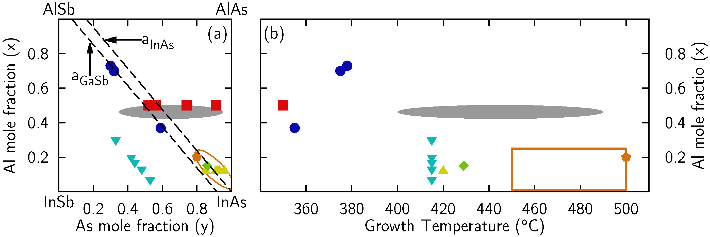
Photonics 03 00020 g001
Figure 2. (a) As mole fraction (y) in Al0.462In0.538AsySb1-y layers with respect to PSb2 at the values for Tg and PAs2 shown in (bd). Lattice-matching (indicated by the dashed line at y = 0.588) is only achieved at 410 C . high resolution x-ray diffraction (HRXRD) measurements around the InAs (004) diffraction of samples grown at (b) 480 C , PAs2 = 1.5 × 10⁻⁵ torr (c) 445 C , PAs2 = 4.7 × 10⁻⁶ torr (d) 410 C , PAs2 = 3.0 × 10⁻⁶ torr . Fully strained films are found for samples grown at intermediate PSb2 values at 410 °C and 445 C . PSb2 in the subfigures (bd) given in 1 × 10⁻⁶ torr starting from the left most peak: (b): 2.13 0.99 (c): 2.57 1.19 1.00 0.54 0.00 (d): 2.55 1.19 0.58 0.39 0.24 0.00.
Photonics 03 00020 g002
Figure 3. AFM of samples grown at 445 C (ad) 410 C (eh) with root mean square roughness values (Rq). PSb2 is increased left-to-right. Samples grown at low PSb2 show crosshatch due to the high lattice mismatch (a,b,e). At intermediate PSb2, smooth films are obtained (c,d,f,g). At high PSb2, high surface roughness is observed (h), scale bar = 2 μ m . Peak-to-valley values are: (a) 15.9 n m ; (b) 3.2 n m ; (c) 3.9 n m ; (d) 6.4 n m ; (e) 23.7 n m ; (f) 1.8 n m ; (g) 1.5 n m ; (h) 44.2 n m .
Photonics 03 00020 g003
Figure 4. AFM of samples grown at 445 C at PSb2 = 1.0 × 10⁻⁶ torr and 2.5 × 10⁻⁶ torr . PAs2 is increased left-to-right. At both values of PSb2 smooth films were obtained at a PAs2 of 4.8 × 10⁻⁶ torr . When PAs2 is reduced below this value, the roughness is increased dramatically. This is even more pronounced at the higher value of PSb2, indicating that this behavior is not caused by a too low total group V flux. It can be concluded that in absence of As, high values of PSb2 are causing the roughening of the surface. Growing Al0.462In0.538AsySb1-y at PSb2 of 1 × 10⁻⁶ torr and PAs2 of 6.4 × 10⁻⁶ torr leads to a high lattice mismatch, which is causes crosshatch and an increased surface roughness. Scale bar = 2 μ m . Peak-to-valley values are: (a) 236.2 n m ; (b) 6.4 n m ; (c) 103.6 n m ; (d) 6.9 n m ; (e) 2.9 n m ; (f) 13.2 n m .
Photonics 03 00020 g004
Figure 5. (a) Arsenic mole fraction and (b) root mean square surface roughness (Rq) of Al0.462In0.538AsySb1-y with respect to PAs2, at two different PSb2 values and Tg = 445 C . Lattice matching with InAs is indicated by the dashed line in (a). By decreasing PAs2, the As fraction in the grown layer is decreased. The minimum of the surface roughness was found around PAs2 = 4 × 10⁻⁶ torr . Below PAs2 = 3 × 10⁻⁶ torr no epitaxial grown is possible under these conditions.
Photonics 03 00020 g005
Figure 6. Samples that exhibited high surface roughness but no cross hatch in the AFM analysis have been measured by SEM. (a) corresponds to Figure 4c: Tg = 445 C , PAs2 = 2.9 × 10⁻⁶ torr , PSb2 = 1.0 × 10⁻⁶ torr . 3-D island growth, caused by a low As2 coverage of the sample, was found. Energy dispersive X-ray spectroscopy (EDX) measurements show homogeneous distributions of Al, In, As and Sb; (b) corresponds to Figure 3h: Tg = 410 C , PAs2 = 3 × 10⁻⁶ torr , PSb2 = 2.55 × 10⁻⁶ torr . 3-D island growth, seem to be caused by a too high Sb2 flux. Al, In, As and Sb are homogeneously distributed according to the EDX analysis; (c) corresponds to Figure 4a: Tg = 445 C , PAs2 = 3.3 × 10⁻⁶ torr , PSb2 = 2.5 × 10⁻⁶ torr . Octagonally shaped, well order crystallites are found on this samples. The EDX study shows that the crystallites are rich in Sb with respect to the surrounding area. Scale bar = (4 μ m).
Photonics 03 00020 g006
Figure 7. Summary of all samples used in this study that have been grown at Tg = 445 C (a) and 410 C (b). At both Tg, high PAs2/PSb2 ratios lead to cross hatch due to a large lattice mismatch. For a Tg of 445 C , PAs2 below 3.3 × 10⁻⁶ torr leads to a rough surface. Growth performed at high PSb2 leads to the formation of crystallites which suggest that the material is decomposing due to the miscibility gap. At higher values of PAs2 high quality material is grown. At this Tg the region in which lattice matching can be achieved is close to the region for which the formation of crystallites is observed. Samples grown at a Tg of 410 C show roughening of the surface at high PSb2. At this Tg the region in which lattice matching is possible is far away from the region in which surface roughening was found.
Photonics 03 00020 g007

