Abstract
Heterogeneous crystalline semiconductor nanomembrane (NM) integration is investigated for single-layer and double-layer Silicon (Si) NM photonics, III-V/Si NM lasers, and graphene/Si NM total absorption devices. Both homogeneous and heterogeneous integration are realized by the versatile transfer printing technique. The performance of these integrated membrane devices shows, not only intact optical and electrical characteristics as their bulk counterparts, but also the unique light and matter interactions, such as Fano resonance, slow light, and critical coupling in photonic crystal cavities. Such a heterogeneous integration approach offers tremendous practical application potentials on unconventional, Si CMOS compatible, and high performance optoelectronic systems.
1. Introduction
Heterogeneous integration is one of the highly demanded technique for a long time in the semiconductor industry. Both emerging photonic applications and high-speed electronic applications benefit from the co-integration of compound semiconductors and silicon materials. By combining the benefits of the traditional Si CMOS technology and the superior properties of III-V materials, high-performance electronic/photonic structures and devices can be realized based on the heterogeneous integration of compound semiconductors and silicon. The same technique can be extended to co-integrate III-V and Ge CMOS to create new hybrid CMOS integration circuits. As III-V materials are outstanding for electron transport [1] and SiGe-MOSFET is preferable for holes, the co-integration circuit architectures that combine both types of transistors will be able to realize high performance at low power as desired for mobile applications.
Inorganic crystalline semiconductor nanomembranes (NMs) with thicknesses of a few nanometers to sub-micrometers, different from their bulk or even film counterparts, can offer many unique, superior features toward emerging frontiers of semiconductor nanotechnology research. Originally explored in the Bell Lab in 1990 [2], with the most successful commercialization in SOI (silicon on insulator), crystalline NMs have been experimentally transferred and stacked onto foreign substrates, including both rigid (e.g., silicon and glass) and flexible (e.g., plastics and polymers) substrates [3,4,5,6,7,8,9,10,11,12,13,14,15]. Over the past few years, a polydimethylsiloxane (PDMS) stamp transfer printing process, pioneered by Rogers et al. [3,16], has been developed for the transfer of crystalline semiconductor NMs onto any substrates, for multi-layer stacking and integration onto silicon, glass, or polymer substrates [3,4,14,17,18,19]. Based on this disruptive NM platform, a new class of photonic structures and devices has been demonstrated [3,4,8,12,14,17,18,19,20,21,22,23,24,25,26].
Transfer printing that deals with semiconductor NMs has several variants but all of them involve the release of the functional layers (e.g., crystalline semiconductor NMs) or structures (e.g., fabricated devices) from the starting substrate, and transfer of the functional layers or structures onto a foreign substrate. High etching selectivity is desired to minimize the damage on the membrane layer. A SiO2 buried layer is used for the release of Si and Ge NM layers, while III-V NM layer should be epitaxially grown on the lattice matched sacrificial layer. A generic process of transfer printing is illustrated in Figure 1. A buried (sacrificial) layer needs to be carefully selected in between the top functional device layer and the bottom original substrate as the starting material (Figure 1a), which will be removed by selective etching to release the semiconductor nanomembrane (Figure 1b). The top layer, then, gently falls and bonds with the handling substrate with weak van der Waals force. A PDMS stamp (or other protocols) will be used to pick up the NM and transfer print onto the new foreign substrate (Figure 1c).

Figure 1.
An illustration of the generic process for nanomembrane (NM) transfer printing. (a) NM on the original substrate with a sacrificial layer in-between; (b) NM released from the original substrate by selective removal of the sacrificial layer; (c) NM transfer printed onto a foreign substrate.

Benefit from the unique transferable and flexible features of semiconductor NMs, the transfer on demand idea is expected to be feasible in die-to-die or die-to-wafer applications; the heterogeneous integration of NMs is simply achievable, without the restriction of lattice mismatch which is the most challenging roadblock in conventional heterogeneous integration. Furthermore, enabled by the transfer printing on flexible substrates, many unconventional wearable, conformal optoelectronic devices/systems can be achieved [27,28,29,30,31].
2. Transfer Printing of Silicon NM
Among all kinds of material choices in a combination of functional layer, substrate, and sacrificial layer, silicon on isolator (SOI) structures are most attractive and gain dominant focus in the field of heterogeneous integration. Due to the superb etching selectivity from Si to SiO2, the top SiNM can be simply released by a common buffered hydrofluoric acid (BHF) solution, and the resulting single crystalline SiNMs (tens-hundreds nanometers thick) exhibit excellent properties on strength, flexibility, and stretchability. In this section, we will review some novel optical reflectors and filters which we demonstrated based on SiNM structures on glass or PET substrates via different transfer printing techniques.
2.1. Demonstration of SiNM Reflectors on Glass/Diamond
Traditionally, dielectric multilayer distributed Bragg reflectors (DBRs) exclusively serve for the high reflection, low loss mirrors in those applications that require extremely high reflection such as resonant cavity, lasers, photodetectors, and other essential photonics. Alternatively, one dimensional (1D) single layer sub-wavelength grating (HCG or SWG) was reported, which was ultra-compact and exhibited decent optical properties [32,33,34]. However, the grating structure is hardly transferable due to its isolated strips layout; moreover, its polarization dependent characteristic with the basic grating reflectors further limits its applications.
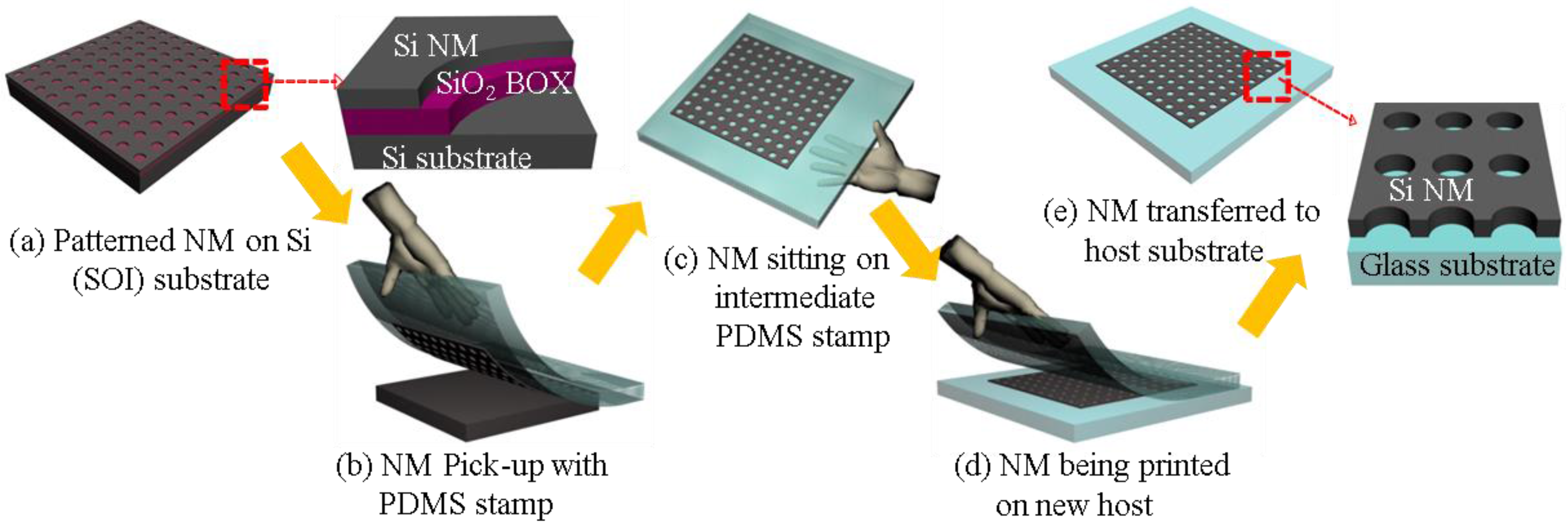
Two-dimensional (2D) photonic crystal slab (PCS) structures, on the other hand, can realize both polarization dependent and independent operations, supported by dispersion and structure designs [35]. More importantly, the single layer PCS structure is mechanically interconnected which makes it robust, flexible, and transferrable. We have previously demonstrated SiNM based 2D PCS broadband reflectors on both SOI substrates and glass substrates [36,37]. The PDMS-assisted NM printing process, also called “dry” transfer printing process, is illustrated schematically in Figure 2. The Si membrane reflector (MR) was first fabricated on the SOI substrate (Figure 2a), followed by patterned Si NM release process, by immersing the patterned SOI substrate in BHF solution to chemically remove a buried oxide layer. A PDMS stamp, with an optimal adhesion force, was used to pick up the released/detached, patterned Si MR structure (Figure 2b). With the PDMS stamp as a transfer media (Figure 2c), the patterned Si MR structure was then transfer printed to the foreign substrate (glass in this case, Figure 2d). Special care was taken on the PDMS stamp itself and the NM pick-up and print (peel-off PDMS) speed. A constant speed during the entire printing process and optimal handling force were applied.

Figure 2.
A NM printing process flow with a PDMS stamp. (a) Fabricated Si MR on a SOI substrate; (b) Top Si NM is released and picked up by a PDMS stamp; (c) Si NM is intermediately transferred on PDMS stamp; (d) Si NM is being printed on recipient (glass) substrate; and (e) Transferred SiNM on final glass substrate. Reproduced with permission from [37].
The microscopic and the scanning electron microscope (SEM) images of the transfer printed Si MR on glass substrate is shown in Figure 3a,b, the 2D PCS has been successfully transferred without any visible defects. The measured and simulated reflection spectra agree well, and the spectral blue-shift is observed after transfer as expected, due to the relatively lower refractive index of the glass substrate. The PDMS stamp associated transfer printing technique developed here can also be applied to other types of materials and structures.
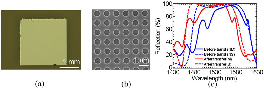
Figure 3.
Transfer printed SiNM PCS on glass. (a) Microscope image of Si MR on a glass substrate; (b) SEM zoom-in image; (c) Measured and simulated reflections. Reproduced with permission from [37].
Figure 3.
Transfer printed SiNM PCS on glass. (a) Microscope image of Si MR on a glass substrate; (b) SEM zoom-in image; (c) Measured and simulated reflections. Reproduced with permission from [37].

Recently, employing the similar transfer printing technique, we have successfully demonstrated athermal Si MRs on diamond substrates [38]. Thermal engineering of the cavity to enable excellent heat dissipation from the active region and to minimize the temperature rise of the lasing cavity is of great importance towards ultra-compact uncooled lasers operating over wide temperature ranges, and high power lasers with simplified thermal mechanical designs. Structural thermal performance was investigated on the transfer printed Si MR on diamond. Figure 4a shows the SEM top-view image of a Si MR with 1 × 1 mm2 pattern area fabricated on the SOI substrate. The Si MR was first released from the SOI substrate and then transferred onto the diamond substrate (Optical grade polycrystalline CVD diamond from Element Six Corp), based on PDMS transfer printing technique. The transferred Si MR on diamond was shown in Figure 4b and the quality is pretty good although the surface of the diamond substrate is a little rough with some black dots. Shown in Figure 4c,d) are the measured and simulated reflection spectra of Si MR with incident light from the diamond substrate side, and the top Si MR air side, respectively. We can see that the measured and the simulated reflections match very well. The reflection from the substrate side is close to 95% over 150 nm wavelength range from 1300 nm to 1450 nm. The estimated reflection measurement error is around 1%–2%, which is mainly associated with the scattering losses on the rough surface, and the focused non-collimated incident beam, which results in non-ideal surface-normal incidence. The reflection performance can be further improved by using polished diamond substrate with much small surface roughness to improve the transfer quality or single crystalline diamond substrate to reduce inner light scattering.
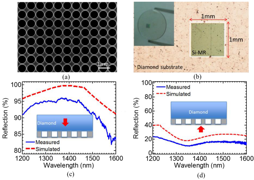
Figure 4.
Si MRs transfer on diamond substrate. (a) A SEM image of PC structure patterned on SOI; (b) Optical microscopic images of Si MR reflector transferred on diamond substrate, with the inset shown the complete view; (c) Measured and simulated reflection spectra for Si MR on diamond with incidence from the diamond substrate side; and (d) with incidence from top Si MR side. Reproduced with permission from [38].

In a typical “dry” transfer printing process of SiNM 2D PCS structures, the ratio of air hole size (radius r) to the spacing (a) is crucial. More challenges rise when the r/a ratio increases, as the physical contract area between PDMS stamp and SiNM becomes smaller. In this review, we have experimentally transferred SiNM 2D PCS with a r/a of 0.28 [37] and 0.45 [38].
2.2. Demonstration of SiNM Fano Filters on Glass/PET
Other than the PDMS stamp associated “dry” transfer printing method discussed above, a “wet” flip transfer printing method was also developed by applying an adhesive (such as SU-8) to improve adhesion and mechanical stability of the final device [39,40]. Similar to the dry transfer printing method, the 2D PCS structure was first fabricated on SOI wafer using a standard e-beam lithography technique and an HBr/Cl2 chemistry based reactive-ion etching (RIE). Once the top patterned SiNM was completely released by BHF, it was rinsed in de-ionized (DI) water and then transferred onto glass or PET substrates by a flip transfer (SiNM was picked up by the foreign substrate coated with an adhesive layer), where an adhesive layer was prepared on the glass substrate prior to transfer. As shown in Figure 5, the SEM image and measured transmission spectrum indicate a high quality SiNM PCS Fano filter transferred on the glass substrate. The Fano resonance phenomenon is manifested by the presence of a discrete state (in plane guided resonant mode) coupled with a continuum of states (vertical radiation modes) [20,41]. The “wet” flip transfer printing method is most desirable in the cases where an adhesive layer has no impact or sometimes preferred as an optical buffer material.
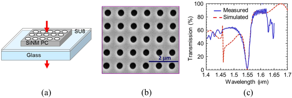
Figure 5.
A SiNM PCS Fano filter realized by the “wet” flip transfer printing method. (a) Transferred SiNM PC membrane filter on a glass substrate; (b) SEM zoom-in view; (c) Measured and simulated transmission. Reproduced by permission of the Institution of Engineering and Technology [39].
Figure 5.
A SiNM PCS Fano filter realized by the “wet” flip transfer printing method. (a) Transferred SiNM PC membrane filter on a glass substrate; (b) SEM zoom-in view; (c) Measured and simulated transmission. Reproduced by permission of the Institution of Engineering and Technology [39].

2.3. Demonstration of Coupled Double-Layer SiNM Fano Filters with Shifted Lattice
Optical filters based on single layer 2D PCS have been investigated extensively, however, single layer PCS Fano filters suffer from limited dispersion engineering capabilities for fine-tuning the output spectrum. A decade ago, coupled bi-layer PCS structures were proposed theoretically [42], which can engineer Q factors by precisely tuning the gap and the lattice displacement between two coupled PCS. Ideally, infinite Q factors can be achieved in coupled bi-layer PCS. However, experimental demonstration of coupled double-layer PCS structures with controlled lattice displacement had not been realized until the PDMS transfer printing technique was employed, due to the fabrication challenges in processing two single crystalline SiNM PCS with controlled shift lattice. We recently reported a successful demonstration of coupled double-layer PCS with precisely controlled lattice displacement, based on large area SiNM transfer printing and multi-layer e-beam alignment processes [43]. The detailed fabrication process flow is illustrated in Figure 6.
A thin SiO2 buffer layer was first formed by thermal oxidation on a SOI substrate (Figure 6(b1)), then the Cr/Au global alignment cross marks were defined by e-beam lithography (EBL) and lifted-off (Figure 6(b2)), followed by Si PCS EBL patterning and RIE etching of the bottom Si PCS layer ((Figure 6(b3)). Meanwhile, another piece of single crystalline SiNM was released from an unpatterned SOI substrate and picked up by a PDMS stamp (Figure 6(a1–a3)). After that, the SiNM was transfer printed on top of the patterned bottom Si PCS (Figure 6c,d)). Finally, aided by the alignment marks made on the bottom PCS layer, the top SiNM was patterned following similar processes shown in (Figure 6(b1–b3)) to form top Si PCS layer with controlled lattice offset and alignment accuracy about 10 nm (Figure 6e).
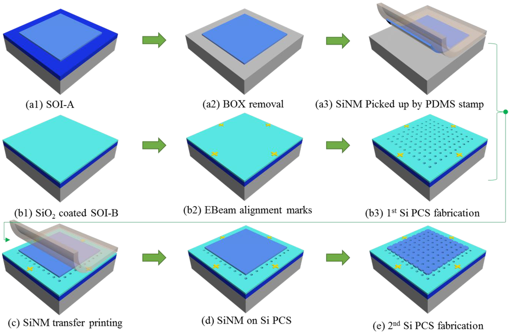
Figure 6.
Schematic of double-layer lattice-shifted SiNM PCS fabrication process. (a1) Starting SOI substrate A (top SiNM pre-defined); (a2) Buried Oxide layer removal; (a3) Released SiNM picked up by a PDMS stamp; (b1) Starting SOI substrate B (a thermal SiO2 pre-coated); (b2) Globe e-beam alignment Cr/Au marks formation; (b3) 1st Si PCS e-beam lithography (EBL); (c) SiNM transfer printing via a PDMS stamp; (d) Transfer printed SiNM on e-beam panted Si PCS; and (e) 2nd SiNM PCS EBL with alignment.

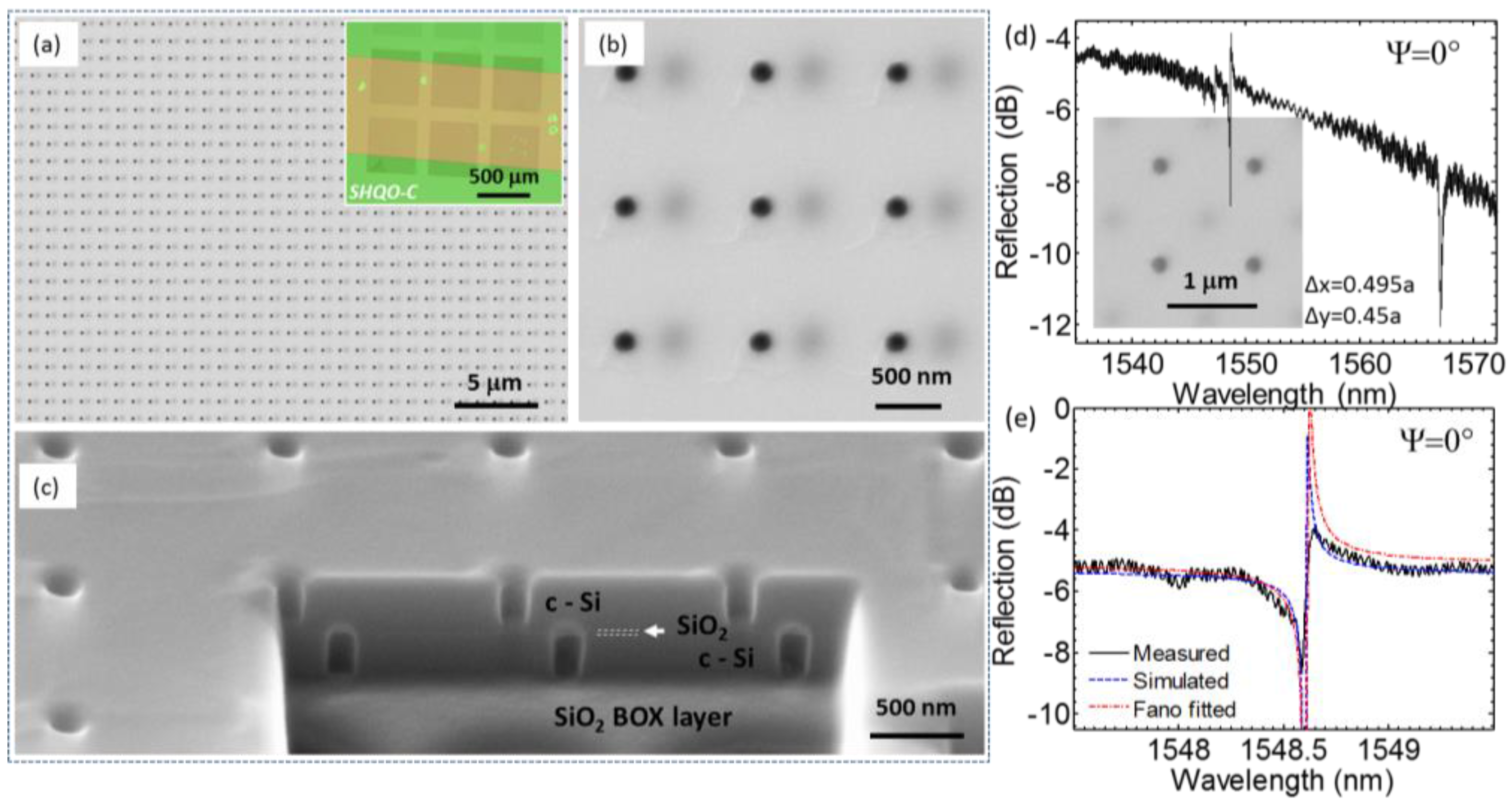
A fabricated double layer PCS Fano filter with precise control of lattice displacement between the top and bottom PCS layers was shown in Figure 7. Shown in Figure 7a is a top view SEM micrograph for a fabricated device, with an optical micrograph of 6 patterned devices shown in the inset. A zoom-in SEM image is shown in Figure 7b. The cross-sectional view SEM image shown in Figure 7c, prepared by the focus ion beam (FIB) process, clearly reveals coupled double layer PCS structures with precisely controlled lattice displacement. Shown in Figure 7d,e are the measured reflection results from a large lattice displacement (Δx = 0.495a, Δy = 0.45a, where a is the lattice constant of the PCS structure). We obtained a measured Q factor of 80,000, agreeing well with the simulated value of 130,000 in this case.
The transfer printing of a large-area single-crystalline SiNM played the most important role in realizing such lattice-shifted double-layer PCS structures. The process developed here can be extended to even broader applications, such as multi-layer homogeneously/heterogeneously integrated systems where high quality single crystalline semiconductors and fine control of lattice placement are simultaneously required.

Figure 7.
Fabricated double layer 2D PCS. (a) Top view SEM image; (b) Zoom-in view; (c) Cross-sectional view; (d) Measured reflection spectrum of a large offset; and (e) Zoom in plots around the dominant resonance with measured, simulated, and Fano fitted reflection spectra. Reproduced with permission from [43].
3. Transfer Printing of III-V Group NM
By employing the semiconductor NM transfer printing process, we have demonstrated 2D PCS based MRs and MR-vertical-cavity surface-emitting lasers (VCSELs) on Si substrate [14,44,45]. In this section, we will review the transfer printing technique involving III-V compound semiconductors, with our experimental demonstration of MR-VCSEL structures.
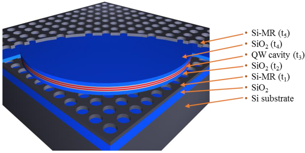
Figure 8.
Schematic of MR-VCSEL lasing cavity structure, which consists of five layers (t1–t5): an InGaAsP QW cavity sandwiched between two single layer Si Fano resonance PC membrane reflectors (Si-MRs), stacked on a Si substrate. Low index SiO2 buffer layers are inserted to ensure high reflection of MRs.
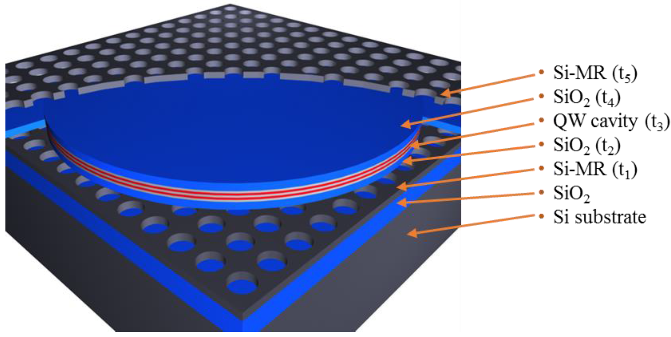
Alternative to the traditional DBR based VCSEL structure, Si MRs were employed as the top and bottom mirrors. As shown schematically in Figure 8, the MR-VCSEL cavity consists of a III-V InGaAsP quantum well (QW) cavity (layer t3), sandwiched between two single-layer Si PC Fano resonance MRs (layers t1 and t5). Two low index buffer layers (SiO2, layers t2 and t4) were inserted to ensure proper index contrast to the top and bottom Si-MRs. The complete MR-VCSEL cavity (t1 to t5) was built on top of a SOI substrate with a SiO2 box layer thickness of t0.
The fabrication process of MR-VCSEL is illustrated in Figure 9. High quality patterned photonic crystal Si reflectors were fabricated via e-beam lithography and RIE process on SOI substrates with 340 nm Si template layer and 2 µm BOX layer. A low-index PECVD SiO2 layer was then deposited on top of the patterned Si to form the bottom MR.

Figure 9.
MR-VCSEL fabrication based on nanomembrane (NM) PDMS stamp printing process. Reproduced with permission from [14].
Figure 9.
MR-VCSEL fabrication based on nanomembrane (NM) PDMS stamp printing process. Reproduced with permission from [14].
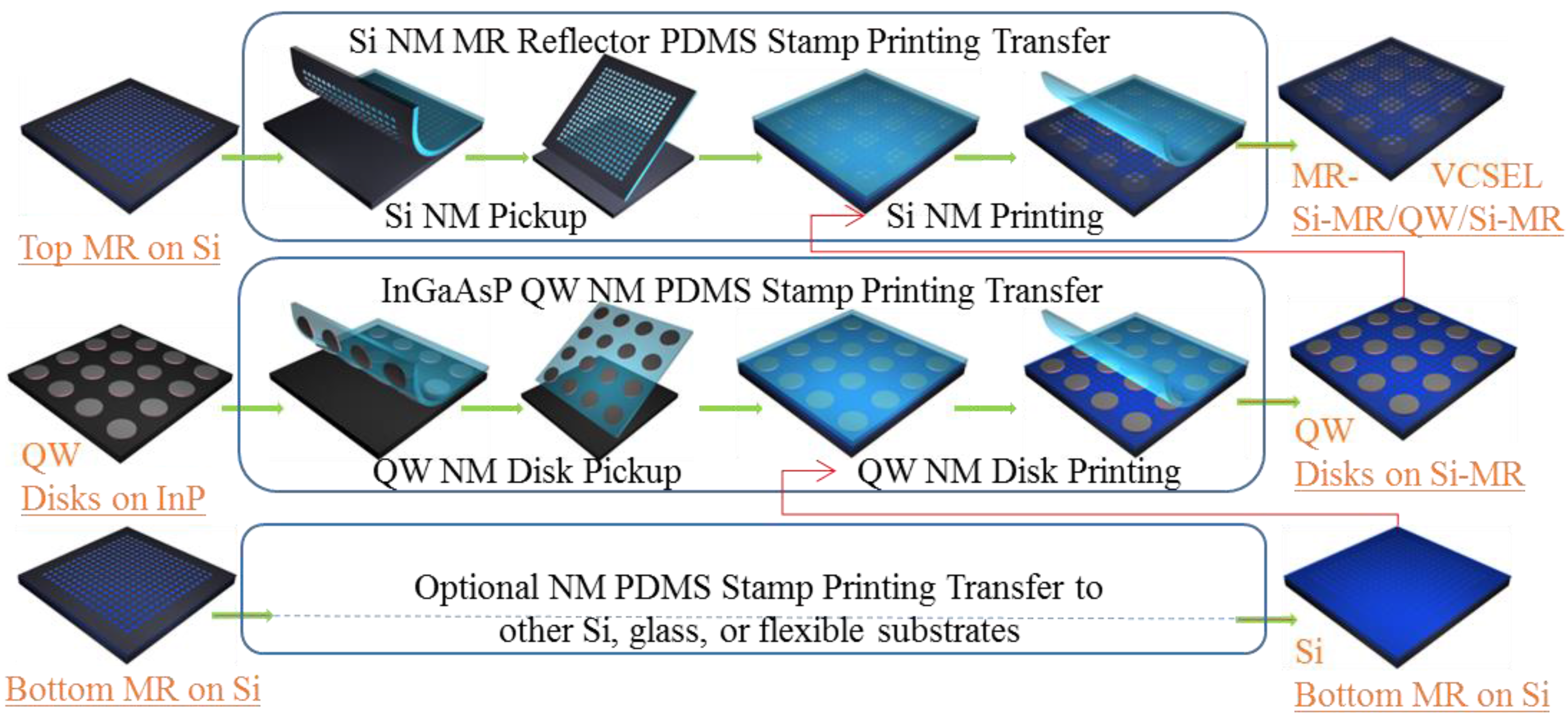
One critical step here is the transfer printing of InGaAsP quantum well (QW) disks. Compared with the SOI based structures, the III-V multi-quantum well (MQW) NM was epitaxial grown on lattice-matched InP substrate, which limits the high etching selectivity between these different III-V materials. Different from the PDMS/SU8 associated transfer printing, here we employed a substrate removal transfer printing with Apiezon black wax as top InGaAsP QW disk protection. The black wax coating was applied right after the InGaAsP QW active disks formed on InP substrate, and the QW disks were released by wet etching away the substrate InP. Then, the released QW disks were consequently transfer printed on top of the bottom Si MR. At this point, the black wax was dissolved by Trichloroethylene (TCE) solvent. On the other hand, the top MR was patterned and released from SOI substrates, and then was transfer printed to a transparent glass substrate. The top Si MR attached to the glass substrate was then transferred to the top of the InGaAsP QW disks to complete the MR-VCSEL device fabrication. Both the top and bottom MR are in the form of a single piece, while the InGaAsP disks are separated from each other, forming an array of disks.
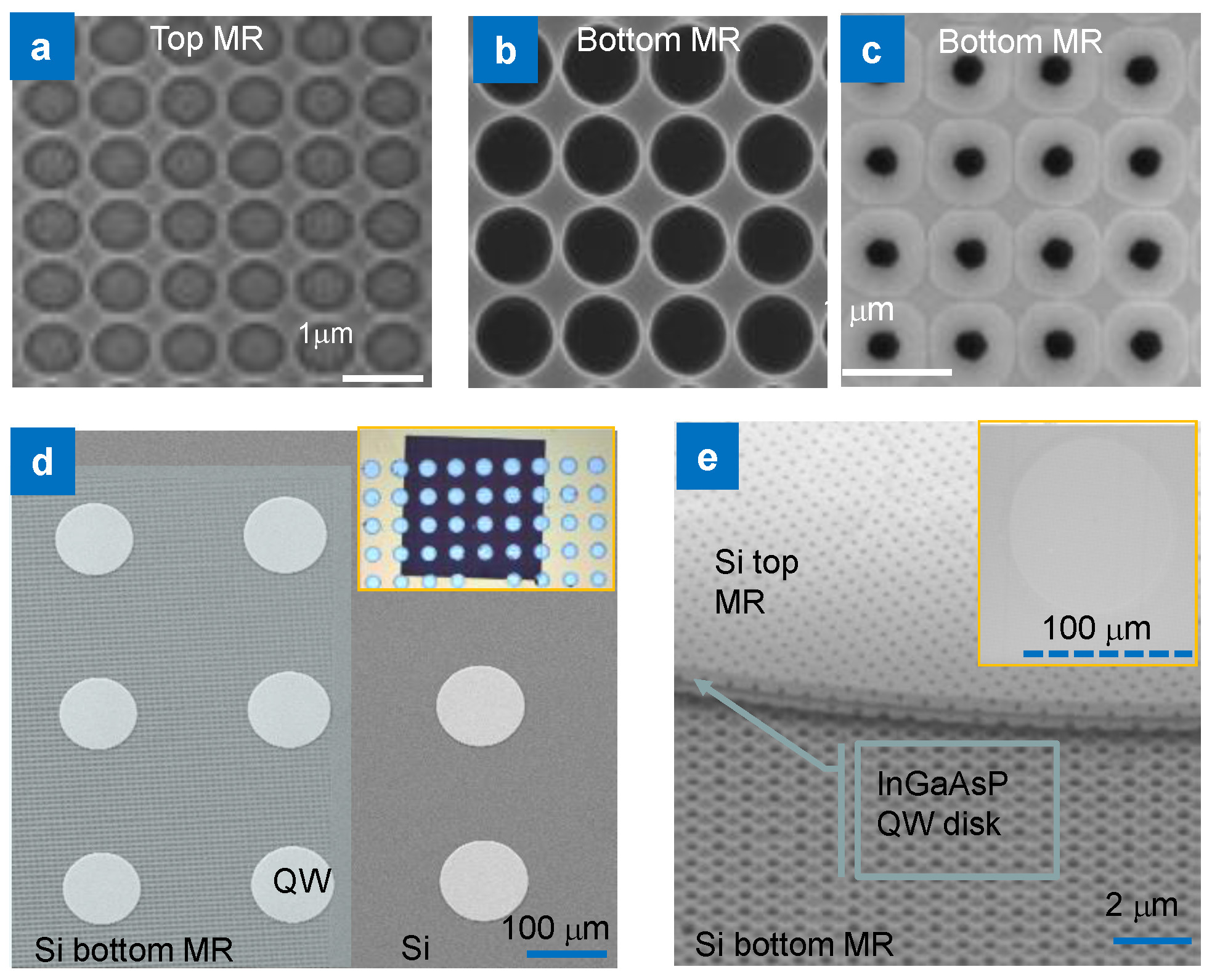
One fabricated MR-VCSEL cavity, operating at low temperature (LT Design), is shown in Figure 10. Shown in Figure 10a is the SEM image of the transferred top MR on glass substrate with a = 860 nm and r/a = 0.46. The bottom Si MR with a = 860 nm and r/a = 0.45 is directly fabricated on a SOI substrate and followed by a deposition of a thin SiO2 film on its top, with a SiO2 layer thickness t2 ~ 383 nm. SEM images before and after the top SiO2 deposition are also shown in Figure 10b and Figure 10c, respectively. Figure 10d shows an SEM image of the InGaAsP QW disks transferred onto the bottom SiMR. Shown here are six QW disks already transferred onto a patterned bottom SiMR region (another two QW disks were laid onto the unpatterned Si region). The diameter D of these QW disks (i.e., the active area of the MR-VCSELs) is 100 μm. Shown in the inset of Figure 10d is a micrograph of fabricated device top view, with QW disks transferred onto a bottom SiMR (the square shaped dark color region). A complete MR-VCSEL structure is shown in Figure 10e, where both the top and the bottom SiMRs are visible, with an inset showing a single QW disk underneath the top SiMR layer. Notice that the total vertical cavity thickness is only 2.4 μm.
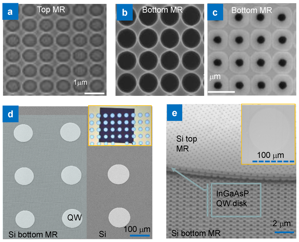
Figure 10.
SEM images and micrographs of membrane reflector (MR) and MR-VCSEL. (a) Top MR transfer printed on glass; (b) Bottom MR on SOI substrate; (c) PECVD coated SiO2 on bottom MR; (d) InGaAsP QW disks/mesas transferred onto a bottom MR. An optical image is shown in the inset; (e) A complete MR-VCSEL device, showing the InGaAsP QW disk sandwiched in between top and bottom Si MRs. Additionally shown in the inset is a SEM top view of InGaAsP QW disk underneath large top Si MR layer Reproduced with permission from [14].
The reflections of these MRs were measured under normal incidence using a slightly focused white light beam and normalized with a gold mirror. The design and measurement results of the top and bottom MRs are summarized in Figure 11a,b. All the reflectors designed and demonstrated here have peak reflection values >99%, with high reflection bands. One can easily find that the measured and simulated reflections are also matched well, which indicate our fabrication techniques were good. One thing we want to mention here is that the small dip at the edge of high reflection band comes from the non-ideal normal incidence, i.e., the slightly focused beam includes a small partial of oblique incident light around the beam edge.
MR-VCSEL device was tested under PL setup using quasi-continuous wave (c.w.) 532 nm laser pumping (with 50% duty cycle). Shown in Figure 11c is the L-L plot (light output for different pump powers) and the corresponding spectral linewidths measured at T = 50 K. The threshold pump power was ~8 mW, or 0.32 KW/cm2. The measured spectral linewidths reduced from 30 nm below threshold to 0.6–0.8 nm above threshold. The measured spectral outputs are shown in Figure 11d, for pump powers below, at, and above thresholds (points (i, ii, iii, iv) at L-L curve). The lasing spectral linewidth was ~8 Å, which is limited by the measurable resolution of the monochrometer. The relative peak location shift shown in Figure 11d from bias levels (ii) and (iii, iv) is mostly related to mode hopping and temperature rise inside the active region at higher pump power levels.
This MR-VCSEL LT device was also characterized at different temperatures up to 120 K. Figure 11a shows the normalized lasing spectra (arbitrary units, a.u.) above the threshold at T = 15 K, 50 K, 70 K, 90 K, 120 K. We can find the lasing peak red shift as T increases and multimode lasing for most T cases at a rate (dλc/dT) close to the simulated 0.088 nm/K. There is a mode hopping occurred below and above the operation temperature of 80 K. As T rises higher than 125 K, we didn’t get any lasing, which is mainly limited by the MR reflector bandwidth except the QW emission becomes weak. The LT design cavity has three lasing wavelengths at 1448 nm (at 10 K), 1478 nm (at 50 K), and 1520 nm (at 120 K). One can clearly find that these lasing wavelengths match well with the cavity resonances.
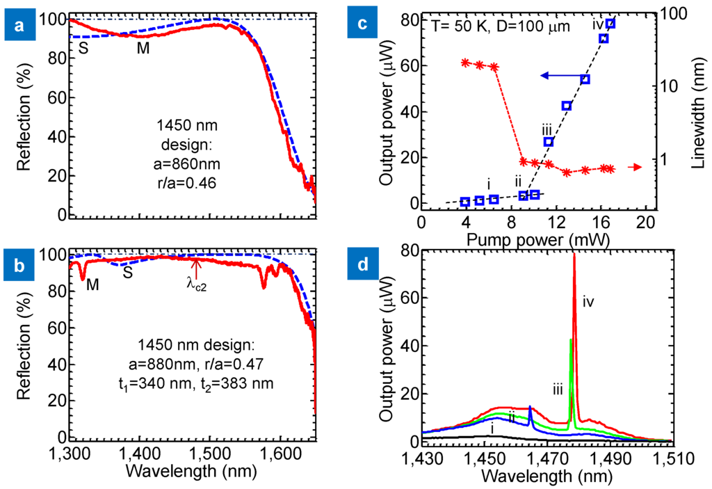
Figure 11.
Reflections of top and bottom membrane reflectors (MRs). (a) and (b) for LT cavity design; (c) The L-L plot (light output for different pump powers) and the corresponding spectral linewidths at T = 50 K; (d) The measured spectral outputs for pump powers below, at, and above thresholds. Reproduced with permission from [14].

In summary, with the advances in Si MR and III-V NM transfer printing techniques, the MR-VCSEL has been demonstrated, with an ultra-compact cavity size and an extremely high finesse optical cavity. However, the laser power efficiency at current stage is still lower than the traditional all III-V epitaxial grown VCSELs. To realize the full potential of MR-VCSELs, an efficient electrical injection scheme has to be incorporated. Additionally, the use of the low index oxide layer presents a bottleneck in the thermal dissipation of QW active region. Different cavity designs and other types of buffer layer materials need to be explored with low refractive index, low optical loss, and high thermal conductivity.
It is worth mentioning that the PDMS stamp associated transfer printing with III-V QW membranes is also feasible, while the exposed side wall of the QW has to be protected to avoid unnecessary lateral etching during the sacrificial removal process. In a recent report, AlInGaAs QW coupons were successfully released by wet etching of Al0.95Ga0.05As sacrificial layer with photoresist layer (Shipley 1827) serving as protection layer as shown in Figure 12a [46]. Then, a PDMS stamp transfer printing process was performed to place the III-V active layer onto Si substrates, thereby forming edge emitting lasers on Si.
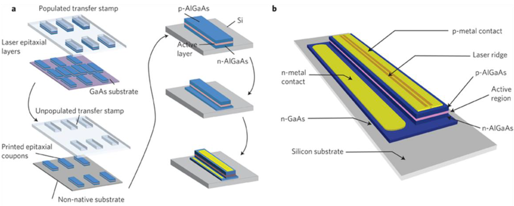
Figure 12.
(a) Schematic of the transfer of unprocessed coupons of epitaxial materials from a native III-V wafer to the host substrate; and (b) Schematic of a laser on the silicon substrate. Reproduced with permission from [46].
Figure 12.
(a) Schematic of the transfer of unprocessed coupons of epitaxial materials from a native III-V wafer to the host substrate; and (b) Schematic of a laser on the silicon substrate. Reproduced with permission from [46].

Another significant challenge in practical large-area III-V is the reliability of III-V NM due to their fragile material property; to overcome such a weak mechanical property, we previously developed the method of strengthen III-V NM by supporting it with an additional metal layer, called a frame-assisted membrane transfer (FAMT) process [47]. Based on this process, 3 × 3 mm2 InP NMs based photodetectors were successfully transfer printed on flexible substrates, while still maintaining their optical/electrical properties.
4. Transfer Printing of Graphene Monolayer
The need of transfer printing of monolayer graphene onto foreign substrates is in demand in most practical applications especially with graphene by chemical vapor deposition (CVD) where the original copper substrate is undesired. An advanced transfer technique was recently developed using a PDMS frame attached to the PMMA/graphene film [48]. As shown in Figure 13, a PMMA supporting layer was spun coated on CVD-graphene on copper foils before the copper was dissolved in the etchant. Then the suspended PMMA/graphene can be transfer printed to any foreign substrates with the PDMS stamp or by a “wet” transfer printing process. A PMMA heat treatment was also used after transfer printing to increase the adhesion and flatness on foreign substrates. More recently, a thermally controlled dry transfer process of patterned graphene layers has been also reported with a demonstration of transparent and wearable electronic/optoelectronic system [49]. Another metal-etching-free direct delamination and transfer of single-layer graphene was demonstrated, too [50].
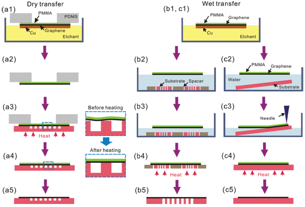
Figure 13.
Schematic illustration of dry and wet transfer process. (a1–a5) Dry transfer onto shallow depressions. Wet transfer onto (b1–b5) perforated substrates and (c1–c5) flat substrates. Reproduced with permission from [48].
Figure 13.
Schematic illustration of dry and wet transfer process. (a1–a5) Dry transfer onto shallow depressions. Wet transfer onto (b1–b5) perforated substrates and (c1–c5) flat substrates. Reproduced with permission from [48].

With the successfully development of SiNM Fano filters that transfer print onto glass substrates [39], we also report experimental demonstrations of the critically coupled total absorption from monolayer graphene at 1550 nm near-infrared wavelength range, based on a two-step transfer printing process to form the desired multi-layer stacking structure on a transparent glass substrate [51].
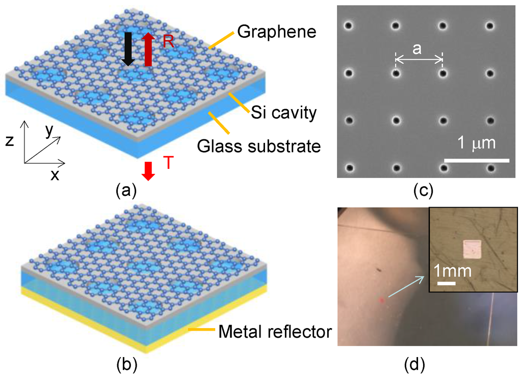
Figure 14.
Schematics of graphene on Si photonic crystal cavity (a) without and (b) with a back metal reflector; (c) a SEM top view image of the fabricated Si photonic crystal slab on SOI substrate; and (d) A micrograph of the device under study here with a tri-layer configuration (monolayer graphene/Si photonic crystal slab/glass substrate) via two step transfer printing processes. Reproduced with permission from [51].

As shown schematically in Figure 14a, the structure considered here consists of a monolayer graphene transferred onto a silicon PCS on a glass substrate. For a symmetric two-port system supporting a single resonance, the theoretical maximum of absorption due to the resonance is 50% [52]. For the system, since the index contrast between silica below the silicon layer and air above the silicon layer is sufficiently small, such that as a simple approximation one can consider this to be a symmetric structure. To achieve total (100%) absorption, a perfect back (metal) reflector was applied, as shown schematically in Figure 14b. Additionaly shown in Figure 14c,d is an SEM image and micrograph of the fabricated device structure on SOI and on glass substrate, respectively.
Si PCS Fano resonance filter was first fabricated on a SOI substrate using e-beam lithography and RIE processes. The top view SEM image of the fabricated photonic crystal structures on the SOI is shown in Figure 14c. After selective-etching the buried oxide of the patterned SOI section with pure hydrofluoric acid, the Si PCS was released (detached from the Si substrate), and transferred onto a glass substrate with PDMS stamp transfer printing process. At this stage, a large-area monolayer graphene, grown on copper substrate by chemical vapor deposition [53], was transferred on top of the Si PCS on glass substrate, with a thin spun-on Poly(methyl methacrylate) (PMMA) layer on top as the graphene transfer supporting layer (wet transfer). Shown in Figure 14d is the micrograph of the patterned Si PCS on a glass substrate, completely covered with a large area monolayer graphene. Since PMMA is optically transparent at operation wavelength around 1550 nm, all simulations and measurements were carried out with a thin (180 nm) PMMA layer on top of the monolayer graphene.

Figure 15.
Measured and simulated (a) transmission and (b) reflection spectra of Si PCS transferred on glass substrate, with the inset in (b) showing the zoom-in of the simulated reflection resonance; (c) Measured transmission and reflection spectra, and derived absorption spectrum for the Si PCS on glass substrate, without graphene layer; and (d) Simulated field distributions for on-resonance and off-resonance modes. Reproduced with permission from [51].
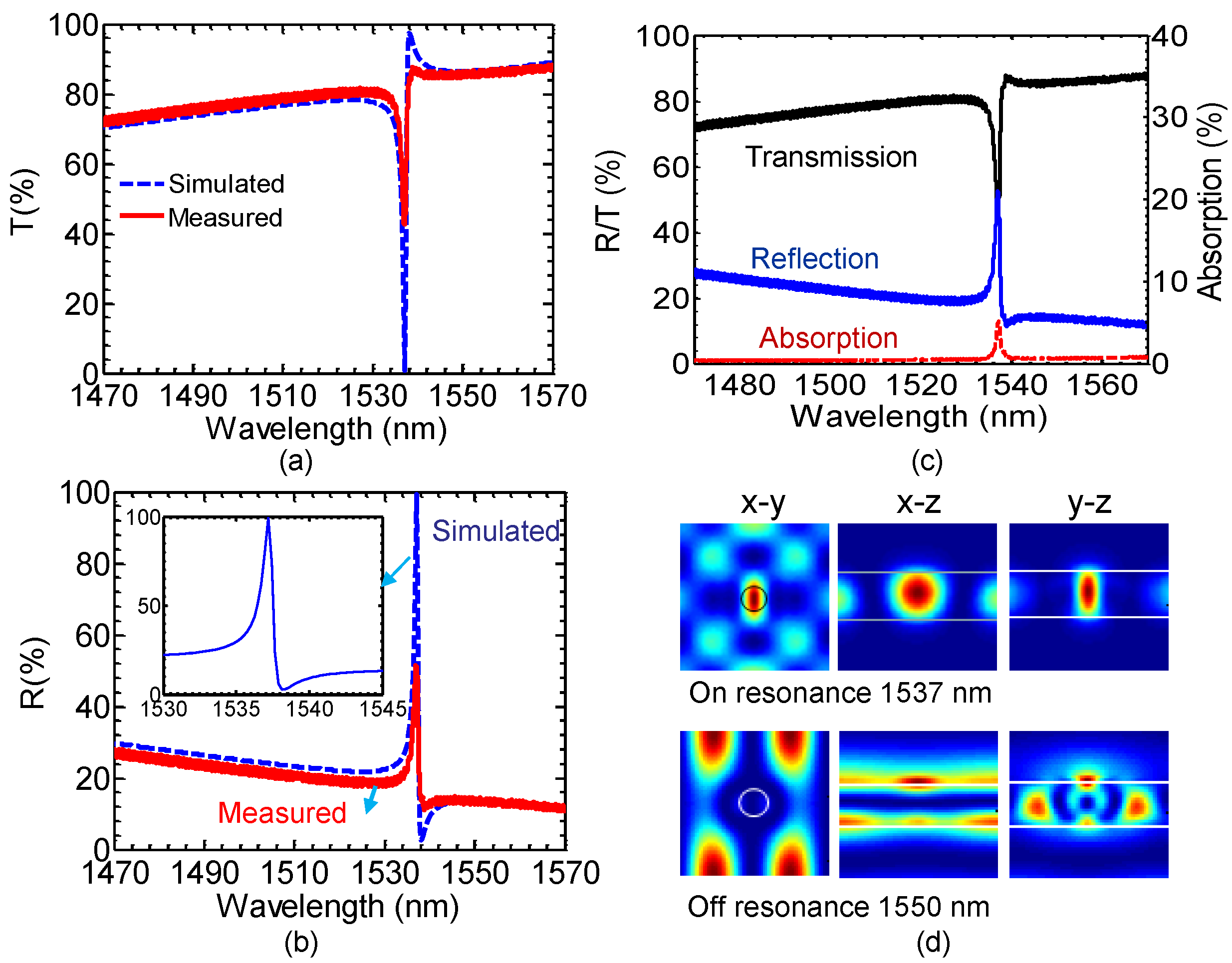
Shown in Figure 15a,b are the measured (solid line) and simulated (dash line) transmission (T) and reflection (R) spectra for the Si PCS Fano filter on glass without the transferred graphene layer. The resonance occurs at 1537 nm with a Q factor of 2100, estimated by fitting with the Fano resonance formula [54]. To establish a baseline/reference on the absorption in the structure, measured absorption (A) spectra for the Si PCS on glass was derived based on A = 1-T-R with the results shown in Figure 15c. Notice that, in theory, the absorption should be zero as Si is non-absorbing at this wavelength region. However, we do see a 5% absorption peak around resonance. This measurement artifact is largely related to the measurement resolution limit and the impact of the non-ideal surface-normal incident angle.
Resonance modal properties were also investigated. Snapshots of the electrical field |E|2 in plane (x-y cross-sectional plane through the center of the silicon slab) and along cross-sectional planes (x-z and y-z planes) are shown in Figure 15d, for on- and off-resonance locations. Well-defined confinement mode can be seen for the on-resonance condition.
After transferring monolayer graphene onto the Si PCS, the device was characterized again by measuring transmission and reflection, as shown in Figure 16a. Notice the measured resonant wavelength red-shifted to 1545.5 nm, as a result of increased index on top, with a monolayer graphene and a 180 nm thick PMMA layer. Both simulation and measurement results agree very well.
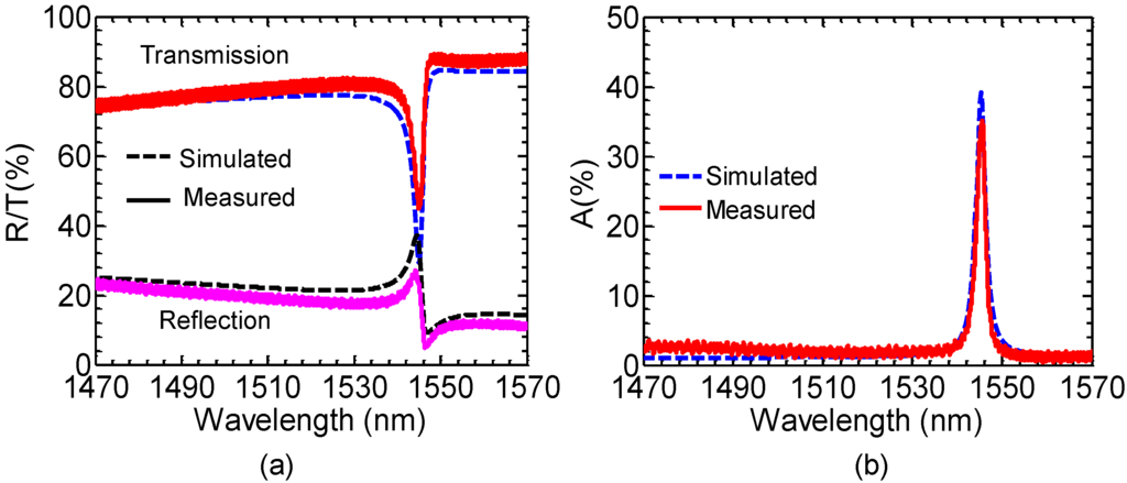
Figure 16.
(a) Measured (solid line) and simulated (dashed line) transmission (T) and reflection (R) spectra for the monolayer graphene on Si PCS without back reflector; and (b) Measured and simulated absorption (A) spectra for the monolayer graphene on Si PCS without back reflector. Reproduced with permission from [51].

In conclusion, monolayer graphene was transfer printed on a silicon photonic crystal Fano resonance filter on a glass substrate. We experimentally obtained peak absorptions of 35% and 85% for cases without and with back reflectors, respectively. The results agree very well with the theoretically estimated values of 39% and 90%, respectively. This work can lead to a wide range of ultra-compact and high performance photonic and optoelectronic devices integrated with graphene monolayer, such as high responsivity, high speed graphene detectors, modulators, light sources, etc.
5. Summary
We reviewed several key photonic devices demonstrated by the heterogeneous integration of single crystalline NMs that involve the semiconductor NM transfer printing technique. Single layer and double layer SiNM PCS structures enabled by transfer printing technique suggest a remarkable approach to address the integration of different single crystalline semiconductor nanomembranes. The III-V NM lasers on Si substrates provide a much more simplified, but reliable approach to realize the surface emission laser source on a Si platform; The graphene and 2D PCS Fano filter based novel total absorption optical components were experimentally demonstrated. The transfer printing integration process can be extend to myriad applications include but not limit to the integrated high efficiency III-V solar cells on Si, multi-/hyper-spectral imaging, 3D photonic/electronic integration and other interdisciplinary applications with its excellent mechanical and thermal merits. The transfer printing technique reviewed here can also be applied to other material systems such as quantum dot film [55], nanoparticles photonic devices [56,57], and stretchable magnetoelectronics [58]. Heterogeneous integration can pave the way for more innovative device designs with novel functionalities and increased performance in future advanced semiconductor applications.
Acknowledgments
The authors appreciate the support from AFOSR (FA9550-08-1-0337, FA9550-09-C-0200, FA9550-11-C-0026, FA9550-11-C-0037, FA9550-13-C-0011, FA9550-09-0-0482, PM: Gernot Pomrenke), ARO (W911NF-09-1-0505, PM: Michael Gerhold), and NSF (ECCS-1308520). The authors also acknowledge current and former group members, and collaborators contributed to the work reported here.
Conflicts of Interest
The authors declare no conflict of interest.
References
- Del Alamo, J.A. The high-electron mobility transistor at 30: Impressive accomplishments and exciting prospects. In Presented at the International Conference on Compound Semiconductor Manufacturing Technology (CS MANTECH), Palm Springs, CA, USA, 16–19 May 2011; pp. 17–22.
- Celler, G.K. Fabrication of dielectrically isolated devices utilizing buried oxygen implant and subsequent heat treatment at temperatures above 1300°C. US Patent 4676841 A, 1987. [Google Scholar]
- Rogers, J.A.; Lagally, M.G.; Nuzzo, R.G. Synthesis, assembly and applications of semiconductor nanomembranes. Nature 2011, 477, 45–53. [Google Scholar] [CrossRef] [PubMed]
- Hwang, S.W.; Tao, H.; Kim, D.H.; Cheng, H.; Song, J.K.; Rill, E.; Brenckle, M.A.; Panilaitis, B.; Won, S.M.; Kim, Y.S.; et al. A physically transient form of silicon electronics. Science 2012, 337, 1640–1644. [Google Scholar] [CrossRef] [PubMed]
- Schmidt, O.G.; Eberl, K. Nanotechnology: solid thin solid films roll up into nanotubes. Nature 2001, 410, 168. [Google Scholar] [CrossRef] [PubMed]
- Trotta, R.; Atkinson, P.; Plumhof, J.; Zallo, E.; Rezaev, R.; Kumar, S.; Baunack, S.; Schröter, J.; Rastelli, A.; Schmidt, O. Nanomembrane quantum light emitting diodes integrated onto piezoelectric actuators. Adv. Mater. 2012, 24, 2668–2672. [Google Scholar] [CrossRef] [PubMed]
- Li, X. Self-rolled-up microtube ring resonators: A review of geometrical and resonant properties. Adv. Opt. Photon. 2011, 3, 366–387. [Google Scholar] [CrossRef]
- Scott, S.A.; Lagally, M.G. Elastically strain-sharing nanomembranes: Flexible and transferable strained silicon and silicon-germanium alloys. J. Phys. D Appl. Phys. 2007, 40, R75–R92. [Google Scholar] [CrossRef]
- Yuan, H.C.; Ma, Z.; Roberts, M.M.; Savage, D.E.; Lagally, M.G. High-speed strained-single-crystal-silicon thin-film transistors on flexible polymers. J. Appl. Phys. 2006, 100. [Google Scholar] [CrossRef]
- Sun, L.; Qin, G.; Seo, J.H.; Celler, G.K.; Zhou, W.; Ma, Z. 12 GHz thin film transistors on transferrable silicon nanomembranes for high performance flexible electronics (cover story). Small 2010, 6, 2553–2557. [Google Scholar] [CrossRef] [PubMed]
- Zhang, K.; Seo, J.H.; Zhou, W.; Ma, Z. Fast flexible electronics using transferrable silicon nanomembranes (topical review). J. Phys. D Appl. Phys. 2012, 45. [Google Scholar] [CrossRef]
- Zhou, W.; Ma, Z.; Yang, H.; Qiang, Z.; Qin, G.; Pang, H.; Chen, L.; Yang, W.; Chuwongin, S.; Zhao, D. Flexible photonic-crystal fano filters based on transferred semiconductor nanomembranes. J. Phys. D Appl. Phys. 2009, 42. [Google Scholar] [CrossRef]
- Zhou, W.; Ma, Z.; Yang, H.; Chen, L.; Yang, W.; Qiang, Z.; Qin, G.; Pang, H.; Chuwongin, S.; Zhao, D. Semiconductor nanomembranes for stacked and flexible photonics. In Proceedings of the International Society for Optics and Photonics, San Francisco, CA, USA, 23 January 2010; p. 76060U.
- Yang, H.; Zhao, D.; Chuwongin, S.; Seo, J.H.; Yang, W.; Shuai, Y.; Berggren, J.; Hammar, M.; Ma, Z.; Zhou, W. Transfer-printed stacked nanomembrane lasers on silicon. Nat. Photon. 2012, 6, 615–620. [Google Scholar] [CrossRef]
- Zhou, H.; Seo, J.-H.; Paskiewicz, D.M.; Zhu, Y.; Celler, G.K.; Voyles, P.M.; Zhou, W.; Lagally, M.G.; Ma, Z. Fast flexible electronics with strained silicon nanomembranes. Sci. Rep. 2013, 3. [Google Scholar] [CrossRef] [PubMed]
- Meitl, M.A.; Zhu, Z.T.; Kumar, V.; Lee, K.J.; Feng, X.; Huang, Y.Y.; Adesida, I.; Nuzzo, R.G.; Rogers, J.A. Transfer printing by kinetic control of adhesion to an elastomeric stamp. Nat. Mater. 2006, 5, 33–38. [Google Scholar] [CrossRef]
- Harazim, S.M.; Quinones, V.A.B.; Kiravittaya, S.; Sanchez, S.; Schmidt, O. Lab-in-a-tube: On-chip integration of glass optofluidic ring resonators for label-free sensing applications. Lab Chip 2012, 12, 2649–2655. [Google Scholar] [CrossRef] [PubMed]
- Song, Y.M.; Xie, Y.; Malyarchuk, V.; Xiao, J.; Jung, I.; Choi, K.-J.; Liu, Z.; Park, H.; Lu, C.; Kim, R.-H. Digital cameras with designs inspired by the arthropod eye. Nature 2013, 497, 95–99. [Google Scholar] [CrossRef] [PubMed]
- Zhou, W.; Ma, Z. Breakthroughs in nanomembranes and nanomembrane lasers. IEEE Photon. J. 2013, 5. [Google Scholar] [CrossRef]
- Zhou, W.; Zhao, D.; Shuai, Y.-C.; Yang, H.; Chuwongin, S.; Chadha, A.; Seo, J.-H.; Wang, K.X.; Liu, V.; Ma, Z. Progress in 2D photonic crystal Fano resonance photonics. Prog. Quant. Electron. 2014, 38, 1–74. [Google Scholar] [CrossRef]
- Hu, J.; Li, L.; Lin, H.; Zhang, P.; Zhou, W.; Ma, Z. Flexible integrated photonics: Where materials, mechanics and optics meet (invited). Opt. Mater. Express 2013, 3, 1313–1331. [Google Scholar] [CrossRef]
- Roberts, M.M.; Klein, L.J.; Savage, D.E.; Slinker, K.A.; Friesen, M.; Celler, G.; Eriksson, M.A.; Lagally, M.G. Elastically relaxed free-standing strained-silicon nanomembranes. Nat. Mater. 2006, 5, 388–393. [Google Scholar] [CrossRef] [PubMed]
- Rogers, J.A.; Someya, T.; Huang, Y. Materials and mechanics for stretchable electronics. Science 2010, 327, 1603–1607. [Google Scholar] [CrossRef] [PubMed]
- Janglin, C.; Liu, C.T. Technology advances in flexible displays and substrates. IEEE Access 2013, 1, 150–158. [Google Scholar] [CrossRef]
- Ko, H.; Takei, K.; Kapadia, R.; Chuang, S.; Fang, H.; Leu, P.W.; Ganapathi, K.; Plis, E.; Kim, H.S.; Chen, S.-Y. Ultrathin compound semiconductor on insulator layers for high-performance nanoscale transistors. Nature 2010, 468, 286–289. [Google Scholar] [CrossRef] [PubMed]
- Chen, Y.; Li, H.; Li, M. Flexible and tunable silicon photonic circuits on plastic substrates. Sci. Rep. 2012, 2. [Google Scholar] [CrossRef] [PubMed]
- Seo, J.H.; Zhang, K.; Kim, M.; Zhao, D.; Yang, H.; Zhou, W.; Ma, Z. Flexible phototransistors based on single-crystalline silicon nanomembranes. Adv. Opt. Mater. 2015. [Google Scholar] [CrossRef]
- Seo, J.-H.; Zhang, Y.; Yuan, H.-C.; Wang, Y.; Zhou, W.; Ma, J.; Ma, Z.; Qin, G. Investigation of various mechanical bending strains on characteristics of flexible monocrystalline silicon nanomembrane diodes on a plastic substrate. Microelectron. Eng. 2013, 110, 40–43. [Google Scholar] [CrossRef]
- Gao, L.; Zhang, Y.; Malyarchuk, V.; Jia, L.; Jang, K.-I.; Webb, R.C.; Fu, H.; Shi, Y.; Zhou, G.; Shi, L. Epidermal photonic devices for quantitative imaging of temperature and thermal transport characteristics of the skin. Nat. Commun. 2014, 5. [Google Scholar] [CrossRef] [PubMed]
- Huang, C.C.; Wu, X.; Liu, H.; Aldalali, B.; Rogers, J.A.; Jiang, H. Large-field-of-view wide-spectrum artificial reflecting superposition compound eyes. Small 2014, 10, 3050–3057. [Google Scholar] [CrossRef] [PubMed]
- Xu, X.; Subbaraman, H.; Kwong, D.; Hosseini, A.; Zhang, Y.; Chen, R.T. Large area silicon nanomembrane photonic devices on unconventional substrates. IEEE Photon. Technol. Lett. 2013, 25, 1601–1604. [Google Scholar] [CrossRef]
- Huang, M.C.Y.; Zhou, Y.; Chang-Hasnain, C.J. A surface-emitting laser incorporating a high-index-contrast subwavelength grating. Nat. Photon. 2007, 1, 119–122. [Google Scholar] [CrossRef]
- Magnusson, R.; Shokooh-Saremi, M. Physical basis for wideband resonant reflectors. Opt. Express 2008, 16, 3456–3462. [Google Scholar] [CrossRef] [PubMed]
- Chang-Hasnain, C.J. High-contrast gratings as a new platform for integrated optoelectronics. Semicond. Sci. Technol. 2011, 26. [Google Scholar] [CrossRef]
- Fan, S.; Joannopoulos, J.D. Analysis of guided resonances in photonic crystal slabs. Phys. Rev. B 2002, 65. [Google Scholar] [CrossRef]
- Yang, H.; Chuwongin, S.; Qiang, Z.; Chen, L.; Pang, H.; Ma, Z.; Zhou, W. Resonance control of membrane reflectors with effective index engineering. Appl. Phys. Lett. 2009, 95. [Google Scholar] [CrossRef]
- Yang, H.; Zhao, D.; Seo, J.-H.; Chuwongin, S.; Kim, S.; Rogers, J.A.; Ma, Z.; Zhou, W. Broadband membrane reflectors on glass. IEEE Photon. Technol. Lett. 2012, 24, 476–478. [Google Scholar] [CrossRef]
- Liu, S.-C.; Zhao, D.; Seo, J.-H.; Liu, Y.; Ma, Z.; Zhou, W. Athermal photonic crystal membrane reflectors on diamond. IEEE Photon. Technol. Lett. 2015, 27, 1072–1075. [Google Scholar] [CrossRef]
- Yang, H.; Pang, H.; Qiang, Z.; Ma, Z.; Zhou, W. Surface-normal fano filters based on transferred silicon nanomembranes on glass substrates. Electron. Lett. 2008, 44, 858–859. [Google Scholar] [CrossRef]
- Qiang, Z.; Yang, H.; Chen, L.; Pang, H.; Ma, Z.; Zhou, W. Fano filters based on transferred silicon nanomembranes on plastic substrates. Appl. Phys. Lett. 2008, 93. [Google Scholar] [CrossRef]
- Johnson, S.G.; Fan, S.; Villeneuve, P.R.; Joannopoulos, J.; Kolodziejski, L. Guided modes in photonic crystal slabs. Phys. Rev. B 1999, 60. [Google Scholar] [CrossRef]
- Suh, W.; Solgaard, O.; Fan, S. Displacement sensing using evanescent tunneling between guided resonances in photonic crystal slabs. J. Appl. Phys. 2005, 98. [Google Scholar] [CrossRef]
- Shuai, Y.; Zhao, D.; Singh Chadha, A.; Seo, J.-H.; Yang, H.; Fan, S.; Ma, Z.; Zhou, W. Coupled double-layer fano resonance photonic crystal filters with lattice-displacement. Appl. Phys. Lett. 2013, 103. [Google Scholar] [CrossRef]
- Ma, Z.; Zhou, W. Hybrid vertical cavity light emitting sources. US Patent 20120228582 A1, 2012. [Google Scholar]
- Zhao, D.; Yang, H.; Chuwongin, S.; Seo, J.H.; Ma, Z.; Zhou, W. Design of photonic crystal membrane reflector based vcsels. IEEE Photon. J. 2012, 4, 2169–2175. [Google Scholar] [CrossRef]
- Justice, J.; Bower, C.; Meitl, M.; Mooney, M.B.; Gubbins, M.A.; Corbett, B. Wafer-scale integration of group iii-v lasers on silicon using transfer printing of epitaxial layers. Nat. Photon. 2012, 6, 610–614. [Google Scholar] [CrossRef]
- Yang, W.; Yang, H.; Qin, G.; Ma, Z.; Berggren, J.; Hammar, M.; Soref, R.; Zhou, W. Large-area inp-based crystalline nanomembrane flexible photodetectors. Appl. Phys. Lett. 2010, 96. [Google Scholar] [CrossRef]
- Suk, J.W.; Kitt, A.; Magnuson, C.W.; Hao, Y.; Ahmed, S.; An, J.; Swan, A.K.; Goldberg, B.B.; Ruoff, R.S. Transfer of cvd-grown monolayer graphene onto arbitrary substrates. ACS Nano 2011, 5, 6916–6924. [Google Scholar] [CrossRef] [PubMed]
- Choi, M.K.; Park, I.; Kim, D.C.; Joh, E.; Park, O.K.; Kim, J.; Kim, M.; Choi, C.; Yang, J.; Cho, K.W. Thermally controlled, patterned graphene transfer printing for transparent and wearable electronic/optoelectronic system. Adv. Funct. Mater. 2015. [Google Scholar] [CrossRef]
- Yang, S.Y.; Oh, J.G.; Jung, D.Y.; Choi, H.; Yu, C.H.; Shin, J.; Choi, C.G.; Cho, B.J.; Choi, S.Y. Metal-etching-free direct delamination and transfer of single-layer graphene with a high degree of freedom. Small 2015, 11, 175–181. [Google Scholar] [CrossRef] [PubMed]
- Liu, Y.; Chadha, A.; Zhao, D.; Piper, J.R.; Jia, Y.; Shuai, Y.; Menon, L.; Yang, H.; Ma, Z.; Fan, S. Approaching total absorption at near infrared in a large area monolayer graphene by critical coupling. Appl. Phys. Lett. 2014, 105. [Google Scholar] [CrossRef]
- Piper, J.R.; Fan, S. Total absorption in a graphene monolayer in the optical regime by critical coupling with a photonic crystal guided resonance. ACS Photon. 2014, 1, 347–353. [Google Scholar] [CrossRef]
- Li, X.; Cai, W.; An, J.; Kim, S.; Nah, J.; Yang, D.; Piner, R.; Velamakanni, A.; Jung, I.; Tutuc, E.; et al. Large-area synthesis of high-quality and uniform graphene films on copper foils. Science 2009, 324, 1312–1314. [Google Scholar] [CrossRef] [PubMed]
- Luk’yanchuk, B.; Zheludev, N.I.; Maier, S.A.; Halas, N.J.; Nordlander, P.; Giessen, H.; Chong, C.T. The fano resonance in plasmonic nanostructures and metamaterials. Nat. Mater. 2010, 9, 707–715. [Google Scholar] [CrossRef] [PubMed]
- Choi, M.K.; Yang, J.; Kang, K.; Kim, D.C.; Choi, C.; Park, C.; Kim, S.J.; Chae, S.I.; Kim, T.-H.; Kim, J.H. Wearable red-green-blue quantum dot light-emitting diode array using high-resolution intaglio transfer printing. Nat. Commun. 2015, 6. [Google Scholar] [CrossRef] [PubMed]
- Son, D.; Lee, J.; Qiao, S.; Ghaffari, R.; Kim, J.; Lee, J.E.; Song, C.; Kim, S.J.; Lee, D.J.; Jun, S.W. Multifunctional wearable devices for diagnosis and therapy of movement disorders. Nat. Nanotechnol. 2014, 9, 397–404. [Google Scholar] [CrossRef] [PubMed]
- Kim, J.; Lee, M.; Shim, H.J.; Ghaffari, R.; Cho, H.R.; Son, D.; Jung, Y.H.; Soh, M.; Choi, C.; Jung, S. Stretchable silicon nanoribbon electronics for skin prosthesis. Nat. Commun. 2014, 5. [Google Scholar] [CrossRef] [PubMed]
- Melzer, M.; Karnaushenko, D.; Lin, G.; Baunack, S.; Makarov, D.; Schmidt, O.G. Direct transfer of magnetic sensor devices to elastomeric supports for stretchable electronics. Adv. Mater. 2015, 27, 1333–1338. [Google Scholar] [CrossRef] [PubMed]
© 2015 by the authors; licensee MDPI, Basel, Switzerland. This article is an open access article distributed under the terms and conditions of the Creative Commons Attribution license (http://creativecommons.org/licenses/by/4.0/).
