
Article

Reversed Size Dependence of External Quantum Efficiency in GaN Micro-LEDs with an AlGaN-Interlayered QW–QD Composite Active Region

1
College of Integrated Circuits and Micro-Nano Electronics, Fudan University, Shanghai 200433, China
2
Suzhou Institute of Nano-Tech and Nano-Bionics, Chinese Academy of Sciences, Suzhou 215123, China
*
Authors to whom correspondence should be addressed.
†
These authors contributed equally to this work.
Photonics 2026, 13(9), 806; https://doi.org/10.3390/photonics13090806
Submission received: 2 August 2026 / Revised: 21 August 2026 / Accepted: 22 August 2026 / Published: 24 August 2026

Abstract

Size-dependent efficiency degradation remains a major challenge for deeply scaled GaN-based micro-light-emitting diodes (micro-LEDs) because etched sidewalls increasingly influence carrier recombination. Here, square micro-LEDs with lateral dimensions of 5–50 μm were fabricated from the same plasma-assisted molecular-beam-epitaxy-grown wafer containing a five-period InGaN quantum-well/1 nm Al0.1Ga0.9N interlayer/InGaN quantum-dot-like (QW–QD) composite active region. Contrary to the conventional size effect, the light output power density and external quantum efficiency (EQE) increased as the mesa size decreased. The peak EQEs were 3.66%, 4.53%, 5.63%, 7.04%, and 7.27% for the 50, 40, 30, 10, and 5 μm devices, respectively, corresponding to an approximately 98.6% increase from 50 to 5 μm. The favorable scaling is consistent with localization-mediated suppression of lateral carrier loss combined with size-dependent light extraction. The present measurements do not quantitatively separate injection, internal efficiency, and extraction contributions. These results demonstrate the potential of ultrathin-interlayer QW–QD active-region engineering for scaled GaN micro-LEDs.

1. Introduction

Micro-light-emitting diodes (micro-LEDs) have attracted considerable attention because of their high brightness, high pixel density, fast response speed, long operational lifetime, and low power consumption. These advantages make micro-LEDs promising candidates for next-generation display applications, including outdoor large-area displays, augmented-reality (AR) and virtual-reality (VR) devices, and automotive head-up displays [1,2,3]. In addition, GaN-based micro-LEDs have shown considerable potential for visible-light communication (VLC) and photonic interconnects owing to their high energy efficiency per bit, large modulation-bandwidth density, excellent thermal stability, and low latency [2,4].
Despite these advantages, several technical challenges still hinder the practical implementation of micro-LEDs in display and communication systems. Among them, the degradation of luminous efficiency with decreasing device dimensions remains a critical issue. In conventional GaN-based micro-LEDs, the external quantum efficiency (EQE) generally decreases as the chip size is reduced, a phenomenon commonly referred to as size-dependent efficiency degradation or the size effect. This behavior is widely attributed to sidewall defects introduced during dry etching. These defects act as carrier-trapping and nonradiative recombination centers, thereby enhancing Shockley–Read–Hall recombination and reducing the internal quantum efficiency; sidewall depletion may additionally perturb current spreading and carrier injection near the mesa perimeter [5,6,7,8].
To mitigate size-dependent efficiency degradation, considerable efforts have been devoted to reducing the density of defects at the etched sidewalls. Tian et al. reduced the sidewall defect density of micro-LEDs by optimizing the post-etch annealing conditions [9]. Wong et al. demonstrated high-efficiency GaN-based micro-LEDs using atomic-layer-deposited passivation layers [10]. Choi et al. further showed that chemical sidewall passivation can suppress perimeter nonradiative recombination in etched InGaN/GaN nanostructures [11]. Zhang et al. suppressed the size effect by combining a fully m-plane-faceted hexagonal mesa with tetramethylammonium hydroxide (TMAH)-based sidewall treatment [12,13]. In addition, Vögl et al. enhanced the light extraction efficiency (LEE) by introducing a backside metal mirror to improve forward emission [14]. Despite these advances, the efficiency degradation associated with device scaling has not been completely resolved. Moreover, additional annealing, wet-chemical treatment, passivation, or optical reflector fabrication generally increases process complexity and may introduce additional interface states, contamination, or process-induced damage.
In conventional InGaN quantum-well (QW) micro-LEDs, carriers are strongly confined along the growth direction but remain relatively free to diffuse laterally within the active region. Consequently, carriers can migrate toward the etched sidewalls, where they may be captured by defect states and undergo nonradiative recombination. This sidewall-related carrier loss becomes increasingly important as the device dimensions decrease because of the increasing perimeter-to-area ratio, resulting in the commonly observed size-dependent efficiency degradation [6,15]. In contrast to two-dimensional QWs, quantum dots (QDs) provide three-dimensional carrier confinement, which can reduce the lateral diffusion of carriers toward the sidewalls. InGaN QDs may also promote strain relaxation and alleviate the polarization-induced quantum-confined Stark effect (QCSE). These characteristics make InGaN QDs attractive candidates for the active regions of micro-LEDs [16,17,18].
Nevertheless, micro-LEDs based solely on InGaN QDs still face several limitations. First, the finite density and carrier storage capacity of QDs may lead to incomplete carrier capture and carrier overflow under high-injection conditions. Second, although QDs can localize carriers, they do not eliminate defects formed elsewhere in the active region, particularly those associated with heterointerfaces. To address these limitations, Wang et al. developed a coupled QW–QD nanostructure grown by metal–organic chemical vapor deposition (MOCVD), in which the QW served as a carrier reservoir while the QDs provided localized radiative recombination states. Using this structure, they demonstrated a 550 nm green LED and a 526 nm superluminescent diode with a degree of polarization of up to 78.7% [19].
In our previous work, we systematically investigated InGaN QW–QD micro-LEDs incorporating (Al)GaN interlayers [20]. A 1 nm Al0.1Ga0.9N interlayer was found to modify the QD morphology and improve the optical performance of 5 μm devices. Those results motivate the present size-series study but do not, by themselves, establish the origin of the size dependence.
Building on the previously optimized active-region structure, the present work focuses on a different question: whether the enhanced optical performance can be maintained as the micro-LED dimensions are progressively reduced. Inspired by the coupled QW–QD concept, we employ an AlGaN-interlayered QW–QD composite active region in GaN-based micro-LEDs grown by plasma-assisted molecular beam epitaxy (PA-MBE). Micro-LEDs with lateral dimensions ranging from 5 to 50 μm were fabricated from the same Al0.1Ga0.9N-interlayered QW–QD epitaxial wafer. The peak EQE increases from 3.66% for the 50 μm device to 7.27% for the 5 μm device. This reversed size dependence is consistent with a reduced contribution of sidewall-related nonradiative recombination to the overall efficiency degradation. Our results provide an active-region-engineering strategy, complementary to conventional sidewall repair and passivation, for improving the efficiency of deeply scaled GaN micro-LEDs.

2. Experimental Section

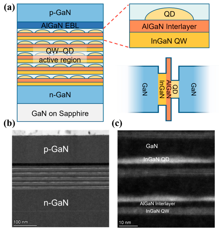
All AlGaN-interlayered micro-LEDs in the size series were fabricated from the same epitaxial wafer to minimize wafer-to-wafer variation within that series. The epitaxial structure was grown by PA-MBE using a Veeco GEN20A system on a GaN template grown on a c-plane sapphire substrate. As schematically illustrated in Figure 1a, the structure consists of a 650 nm Si-doped n-GaN layer, a five-period AlGaN-interlayered InGaN QW–QD composite active region, a 20 nm Mg-doped p-AlGaN electron-blocking layer (EBL), and a 120 nm Mg-doped p-GaN layer. Each active-region period comprises a 4 nm In0.15Ga0.85N QW grown at 650 °C, a 1 nm Al0.1Ga0.9N interlayer grown at 800 °C, an InGaN QD layer grown at 600 °C, and a 12 nm GaN quantum barrier grown at 700 °C. The nitrogen flow rate and RF power of the plasma source were 1.5 sccm and 350 W, respectively. Growth interruptions and substrate-temperature switching were employed between the QW, interlayer, QD, and barrier deposition steps. The remaining PA-MBE active-region growth sequence was the same as that used for the optimized Al0.1Ga0.9N-interlayered sample in our previous work [20]. Figure 1b presents a cross-sectional high-resolution transmission electron microscopy (HRTEM) image of the active region. The QW–QD composite units can be distinguished together with their constituent heterointerfaces.
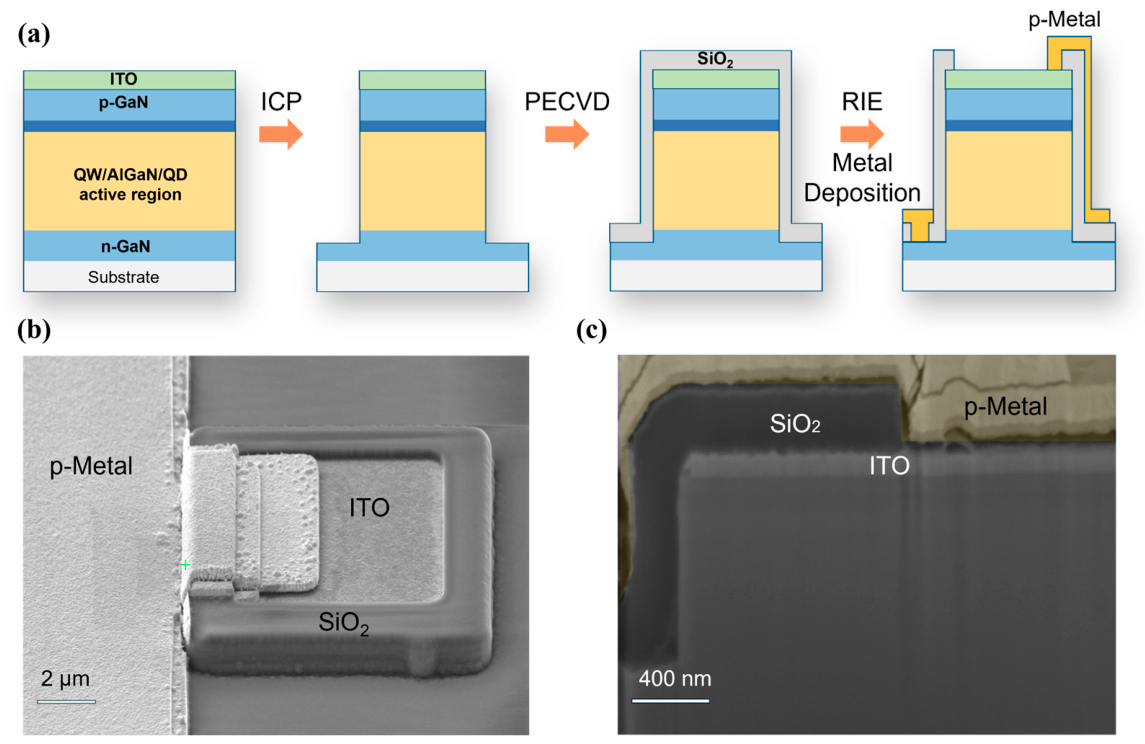
Square micro-LEDs with lateral dimensions of 5, 10, 30, 40, and 50 μm were fabricated from the AlGaN-interlayered epitaxial wafer using identical processing conditions. The fabrication process is schematically illustrated in Figure 2a. First, a 200 nm thick indium tin oxide (ITO) layer was deposited by electron-beam evaporation as a transparent current-spreading layer, followed by rapid thermal annealing at 550 °C in a nitrogen atmosphere. The device mesas were then defined by inductively coupled plasma (ICP) etching. Subsequently, a 200 nm thick SiO2 passivation layer was deposited by plasma-enhanced chemical vapor deposition (PECVD). Finally, Ti/Al/Ti/Au metal stacks with thicknesses of 20/120/60/200 nm were deposited by electron-beam evaporation to form the electrical contacts. To improve the metal coverage and adhesion on the steep micro-LED sidewalls, an additional 20/200 nm Ti/Au bilayer was subsequently deposited by magnetron sputtering. Figure 2b presents a top-view FIB–SEM image of a representative 10 μm micro-LED, and Figure 2c shows a representative cross-section containing the ITO current-spreading layer, dielectric passivation layer, and p-metal contact. Except for the mesa dimension, all devices were fabricated using the same process parameters.
The microstructure of the QW–QD composite active region was examined by high-resolution transmission electron microscopy (HRTEM; Thermo Scientific Themis Z). The surface and cross-sectional morphologies of the fabricated devices were characterized using a focused-ion-beam scanning electron microscope (FIB–SEM; ZEISS Crossbeam 550). Electrical and optical measurements were performed at room temperature under continuous-wave operation. The devices were mounted at the entrance port of an EVERFINE HSF-200 high-sensitivity Micro/Mini-LED electro-optical analysis system, corresponding to a port-mounted 2π integrating-sphere geometry, and a Keysight B2611B source-measure unit was used for electrical biasing. The calibrated spectral radiant flux reported by the HSF-200 for this measurement geometry, Φ e , λ 2 π ( λ ) (W nm−1), was used directly. The system software automatically acquired and subtracted the dark/background signal before spectral integration.
Following the photon-counting definition of LED EQE [21,22], the collected photon rate was calculated over 400–700 nm as
N ˙ γ ( 2 π ) = ∫ 400 n m 700 n m Φ e , λ 2 π ( λ ) h c λ d λ = ∫ 400 n m 700 n m λ Φ e , λ 2 π ( λ ) h c d λ
where h is Planck’s constant, and c is the speed of light in vacuum; wavelength is expressed in SI units in the photon energy factor. The reported EQE was then obtained from
E Q E ( % ) = 100 N ˙ γ ( 2 π ) I q
where I is the measured total device current, and q is the elementary charge. The collected absolute optical power was PLOP(2π) = ∫ 400 n m 700 n m Φ e , λ 2 π ( λ ) dλ. For every device size, the nominal square mesa area Amesa = L2 was used consistently to calculate current density, L is the side length of the etching mesa, the current density J = I/Amesa, and the LOP density is PLOP(2π)/Amesa.
The test system specifies a spectral range of 380–780 nm, a radiant power measurement range of 10−5 mW to 1 mW, and a radiant power accuracy of 3% for signals of at least 0.01 mW [23]. The LOP density and EQE sweeps covered 0–400 A cm−2, and the current density–voltage characteristics were measured from −5 to 6 V.

3. Results and Discussion

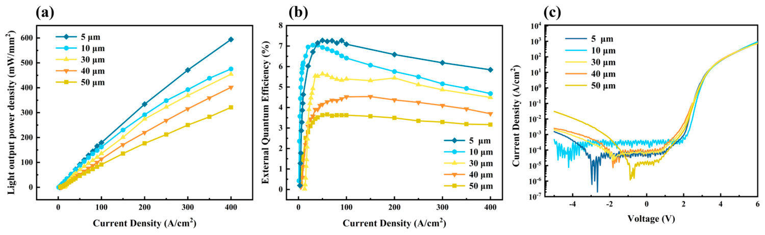
Figure 3a shows the LOP density of the AlGaN-interlayered micro-LEDs as a function of current density. The optical power density increases monotonically with current density for all sizes, and the smaller devices exhibit a higher power density at a given current density. The corresponding EQE characteristics are presented in Figure 3b. Peak EQEs of 7.27%, 7.04%, 5.63%, 4.53%, and 3.66% were obtained at current densities of approximately 50, 7, 20, 70, and 60 A cm−2 for the 5, 10, 30, 40, and 50 μm devices, respectively. Thus, the peak EQE increased by approximately 98.6% as the device dimension decreased from 50 to 5 μm, whereas the peak-EQE current density varied nonmonotonically with mesa dimension. The EQE trend is opposite to the size-dependent efficiency degradation commonly observed in conventional QW-based micro-LEDs [5,6]. Comparable improvements or size-insensitive peak efficiency have been reported when sidewall nonradiative loss is sufficiently suppressed [24,25].
The semilogarithmic |J|–V characteristics in Figure 3c show comparable forward turn-on behavior. The dark current of device decreases as the wafer size gets smaller. However, the reverse leakage current density of the 5 μm device is slightly higher than that of the 10 μm micro-LED under −5 V. The slightly higher leakage current observed in the smaller devices may partly arise from the greater sensitivity of scaled mesa fabrication to process-induced sidewall damage and passivation nonuniformity. In addition, localized leakage paths associated with pre-existing epitaxial defects, such as threading dislocations, could constitute a larger fraction of the total current in devices with smaller active areas. This difference may partly influence the apparent shift of the peak EQE between 5 μm and 10 μm micro-LED by increasing the parasitic current fraction at low injection; however, the present J–V data do not establish leakage as the cause of the nonmonotonic peak-EQE current densities. Residual perimeter-related SRH recombination after SiO2 passivation may also shift an efficiency maximum, although the surface recombination rate was not independently measured. The J–V characteristics provide additional insight into the size-dependent EQE. The 30, 40, and 50 μm devices exhibit comparatively larger leakage current densities than the 5 μm micro-LED. These parasitic leakage channels do not contribute effectively to radiative recombination and may therefore partly account for the higher EQE of the 5 μm micro-LED relative to the larger devices. By contrast, because the leakage current difference between the 5 and 10 μm devices is relatively small, the EQE enhancement of the 5 μm micro-LED over the 10 μm device is more likely associated with localization-mediated suppression of carrier transport toward nonradiative recombination centers. Thus, both size-dependent leakage and carrier localization should be considered when interpreting the reversed size dependence of EQE.
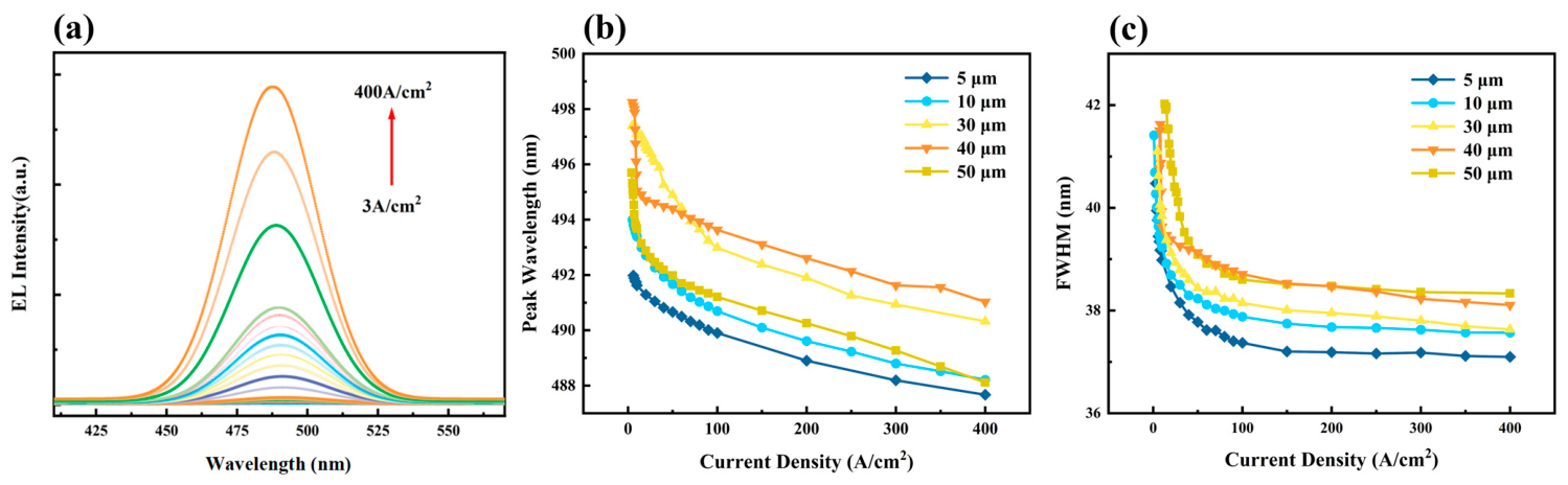
To examine the injection-dependent optical response of the composite active region, peak wavelength and full width at half maximum (FWHM) were analyzed separately. Figure 4a shows unnormalized EL spectra of a representative 5 μm device over 3–400 A cm−2. The spectra remain single-peaked, while the peak shifts to a shorter wavelength as the current density increases. As shown in Figure 4b, as the current density increased from 3 to 400 A/cm2, the peak wavelength blueshifts of the 5, 10, 30, 40, and 50 μm devices were approximately 4.2, 5.8, 7.0, 7.2, and 7.6 nm, respectively, revealing a progressively smaller net spectral shift with decreasing mesa size. Polarization-field screening, filling of localized states, and band filling generally drive a blueshift, whereas self-heating can introduce a competing redshift; spatially heterogeneous localization near etched edges may further modify the net spectral response [26,27,28]. Over the same current density range, the smaller devices, particularly the 5 and 10 μm devices, generally exhibited narrower EL linewidths, as shown in Figure 4c. A narrower linewidth and a smaller peak wavelength shift in smaller devices can be interpreted as a spatial QD ensemble effect. A larger mesa integrates emission from a wider lateral area containing locally different QD sub-ensembles, whose variations in QD size, In composition, residual strain, and localization energy produce a broader distribution of transition energies. A smaller mesa samples a more spatially restricted and energetically concentrated QD ensemble, resulting in a narrower FWHM. Moreover, as the injection density increases, the progressive occupation of deeper QD states can be followed by recombination through shallower QDs or higher-energy QD states. The broader QD energy distribution and less uniform local occupation in larger devices therefore permit more pronounced injection-induced carrier redistribution and a larger ensemble-averaged blueshift. In the smaller devices, the narrower local QD energy distribution and more uniform injection reduce this redistribution, leading to both a narrower linewidth and a smaller peak wavelength shift. Similar size-dependent spectral behavior, including smaller peak wavelength shifts and reduced FWHM broadening in smaller GaN-based micro-LEDs, has also been reported by Dai et al. [29].
The following will further explore how QD-induced carrier localization affects the reversed size dependence observed in micro-LEDs. The external quantum efficiency of an LED is determined by the combined contributions of carrier injection efficiency, internal quantum efficiency, and light extraction efficiency [30,31]:
η E Q E = η i n j × η I Q E × η L E E
where η i n j , η I Q E , and η L E E denote the carrier injection efficiency, internal quantum efficiency, and light extraction efficiency, respectively. In conventional InGaN QW micro-LEDs, carriers are confined along the growth direction but remain relatively free to diffuse laterally within the active region. As the device dimension decreases, the increasing perimeter-to-area ratio increases the fraction of carriers that can reach the etched sidewalls. Plasma-induced defects and surface states at the sidewalls act as Shockley–Read–Hall nonradiative recombination centers, generally resulting in a reduction in EQE for smaller devices [5,7,31].
In conventional InGaN QWs, carrier localization originates mainly from alloy and compositional fluctuations within a quasi-two-dimensional well, so lateral percolation pathways can remain available in the QW plane. In the present composite active region, the intentionally introduced In-rich QD-like morphology provides additional spatially discrete, three-dimensional confinement. Our previous work showed that a 1 nm Al0.1Ga0.9N interlayer reduced the lateral QD dimensions and increased their aspect ratio, consistent with stronger localization [20]. The Al0.1Ga0.9N interlayer introduces conduction- and valence-band offsets that can impede carrier transfer while enhancing carrier confinement. Because the interlayer is only 1 nm thick, tunneling and field-assisted transport across it remain feasible, so the adverse influence of these band offsets on carrier injection into the QD states is negligible, while the interlayer can modify strain, surface energetics, and InGaN nucleation during QD formation. A thicker or higher-Al-content interlayer would be expected to weaken QW–QD electronic coupling.
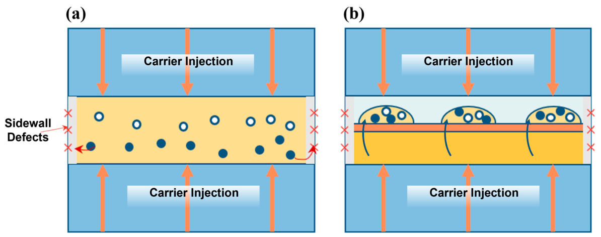
The AlGaN-interlayered size series directly establishes a monotonic increase in peak EQE with decreasing mesa size. Previous studies have shown that once perimeter nonradiative loss is sufficiently limited, the larger sidewall-to-area ratio of smaller mesas can enhance light extraction [24,31,32]. Localization in the QD-like regions may reduce the competing lateral carrier loss channel, thereby allowing this optical benefit to become more visible. To illustrate the carrier transport component of this interpretation, Figure 5 contrasts two limiting pictures of in-plane transport. In a conventional InGaN QW micro-LED, carriers are confined vertically but can diffuse laterally within the QW plane as shown in Figure 5a. A fraction can therefore reach etched sidewalls and recombine nonradiatively at surface and Shockley–Read–Hall centers [5,6,7]. As the characteristic lateral size L decreases, the perimeter-to-area ratio rises (P/A ∝ 1/L). Without a measured diffusion length, this panel does not quantify the associated loss. By contrast, in the AlGaN-interlayered QW–QD stack, carriers captured within the coupled QW–QD manifold are expected to sample the mesa edge less readily than carriers in a delocalized QW continuum, as shown in Figure 5b [20]. The perimeter nonradiative channel may therefore be reduced. The observed EQE scaling is consistent with this localization-assisted suppression of lateral carrier loss acting together with size-dependent light extraction. Figure 5 is offered as a pathway-level working hypothesis without quantifying carrier capture, diffusion length, LEE, or junction-temperature variation.

4. Conclusions

In summary, GaN-based micro-LEDs incorporating an AlGaN-interlayered InGaN QW–QD composite active region were fabricated with lateral dimensions ranging from 5 to 50 μm. Both the light output power density and external quantum efficiency exhibited a favorable dependence on device scaling. The peak EQEs of the 50, 40, 30, 10, and 5 μm devices were 3.66%, 4.53%, 5.63%, 7.04%, and 7.27%, respectively. Thus, reducing the device dimension from 50 to 5 μm resulted in an approximately 98.6% enhancement in peak EQE, in contrast to the conventional size-dependent efficiency degradation commonly observed in QW-based micro-LEDs. The favorable efficiency scaling is consistent with localization-assisted suppression of lateral carrier loss acting together with size-dependent light extraction. The present data do not quantitatively separate carrier injection efficiency, internal quantum efficiency, and light extraction efficiency. Within these evidence boundaries, ultrathin-interlayer QW–QD active-region engineering provides a promising approach for maintaining optical efficiency in deeply scaled GaN micro-LEDs.

Author Contributions

Conceptualization and methodology, Y.G. (Ying Gu) and S.J.; formal analysis and visualization, Y.G. (Yi Gong) and M.J.; investigation, Y.G. (Ying Gu) and M.J.; writing—original draft preparation, Y.G. (Ying Gu) and Y.G. (Yi Gong); writing—review and editing, L.B.; supervision, S.L.; project administration, S.J. and L.B.; funding acquisition, S.J. All authors have read and agreed to the published version of the manuscript.

Funding

This work was supported by the National Key Research and Development Program of China (No. 2023YFB3609800), the Natural Science Foundation of Jiangsu Province (No. BK20230235), the Frontier Technologies R&D Program of Jiangsu (No. BF2025032), and the Suzhou Key Core Technology Project: Leading the Charge with Open Competition (No. SYG2024104).

Institutional Review Board Statement

Not applicable.

Informed Consent Statement

Not applicable.

Data Availability Statement

The data supporting the findings of this research are accessible from the corresponding author upon reasonable request.

Acknowledgments

The authors acknowledge technical support from the Platform for Characterization and Testing and the Nanofabrication Facility of the Suzhou Institute of Nano-Tech and Nano-Bionics, Chinese Academy of Sciences.

Conflicts of Interest

The authors declare no conflicts of interest.

Abbreviations

The following abbreviations are used in this manuscript:
EQEexternal quantum efficiency
EBLelectron-blocking layer
FIB–SEMfocused-ion-beam scanning electron microscopy
HRTEMhigh-resolution transmission electron microscopy
ICPinductively coupled plasma
ITOindium tin oxide
LEElight extraction efficiency
LOPlight output power
micro-LEDmicro-light-emitting diode
PA-MBEplasma-assisted molecular beam epitaxy
PECVDplasma-enhanced chemical vapor deposition
QCSEquantum-confined Stark effect
QDquantum dot
QWquantum well
TMAHtetramethylammonium hydroxide
VLCvisible-light communication

References

  1. Huang, Y.; Hsiang, E.-L.; Deng, M.-Y.; Wu, S.-T. Mini-LED, Micro-LED and OLED Displays: Present Status and Future Perspectives. Light Sci. Appl. 2020, 9, 105. [Google Scholar] [CrossRef] [Scilit] [PubMed]
  2. Lin, C.-C.; Wu, Y.-R.; Kuo, H.-C.; Wong, M.S.; DenBaars, S.P.; Nakamura, S.; Pandey, A.; Mi, Z.; Tian, P.; Ohkawa, K.; et al. The Micro-LED Roadmap: Status Quo and Prospects. J. Phys. Photonics 2023, 5, 042502. [Google Scholar] [CrossRef] [Scilit]
  3. Wierer, J.J., Jr.; Tansu, N. III-Nitride Micro-LEDs for Efficient Emissive Displays. Laser Photonics Rev. 2019, 13, 1900141. [Google Scholar] [CrossRef] [Scilit]
  4. Rajbhandari, S.; McKendry, J.J.D.; Herrnsdorf, J.; Chun, H.; Faulkner, G.; Haas, H.; Watson, I.M.; O’Brien, D.; Dawson, M.D. A Review of Gallium Nitride LEDs for Multi-Gigabit-per-Second Visible Light Data Communications. Semicond. Sci. Technol. 2017, 32, 023001. [Google Scholar] [CrossRef] [Scilit]
  5. Olivier, F.; Daami, A.; Licitra, C.; Templier, F. Shockley-Read-Hall and Auger Non-Radiative Recombination in GaN Based LEDs: A Size Effect Study. Appl. Phys. Lett. 2017, 111, 022104. [Google Scholar] [CrossRef] [Scilit]
  6. Kou, J.; Shen, C.-C.; Shao, H.; Che, J.; Hou, X.; Chu, C.; Tian, K.; Zhang, Y.; Zhang, Z.-H.; Kuo, H.-C. Impact of the Surface Recombination on InGaN/GaN-Based Blue Micro-Light Emitting Diodes. Opt. Express 2019, 27, A643–A653. [Google Scholar] [CrossRef] [Scilit] [PubMed]
  7. Bulashevich, K.A.; Karpov, S.Y. Impact of Surface Recombination on Efficiency of III-Nitride Light-Emitting Diodes. Phys. Status Solidi RRL 2016, 10, 480–484. [Google Scholar] [CrossRef] [Scilit]
  8. Hwang, D.; Mughal, A.; Pynn, C.D.; Nakamura, S.; DenBaars, S.P. Sustained High External Quantum Efficiency in Ultrasmall Blue III-Nitride Micro-LEDs. Appl. Phys. Express 2017, 10, 032101. [Google Scholar] [CrossRef] [Scilit]
  9. Tian, P.; McKendry, J.J.D.; Gong, Z.; Guilhabert, B.; Watson, I.M.; Gu, E.; Chen, Z.; Zhang, G.; Dawson, M.D. Size-Dependent Efficiency and Efficiency Droop of Blue InGaN Micro-Light Emitting Diodes. Appl. Phys. Lett. 2012, 101, 231110. [Google Scholar] [CrossRef] [Scilit]
  10. Wong, M.S.; Hwang, D.; Alhassan, A.I.; Lee, C.; Ley, R.; Nakamura, S.; DenBaars, S.P. High Efficiency of III-Nitride Micro-Light-Emitting Diodes by Sidewall Passivation Using Atomic Layer Deposition. Opt. Express 2018, 26, 21324–21332. [Google Scholar] [CrossRef] [Scilit] [PubMed]
  11. Choi, W.H.; You, G.; Abraham, M.; Yu, S.-Y.; Liu, J.; Wang, L.; Xu, J.; Mohney, S.E. Sidewall Passivation for InGaN/GaN Nanopillar Light Emitting Diodes. J. Appl. Phys. 2014, 116, 013103. [Google Scholar] [CrossRef] [Scilit]
  12. Zhang, P.; Gu, Y.; Gong, Y.; Hua, H.; Jin, S.; Yang, W.; Zhu, J.; Long, S.; Lu, S. Elimination of Size Effects in InGaN Quantum Dot Cyan-Green Micro-LEDs by Constructing a Full-m-Plane Hexagonal Structure. ACS Photonics 2024, 11, 2045–2053. [Google Scholar] [CrossRef] [Scilit]
  13. Zhang, P.; Hua, H.; Gu, Y.; Gong, Y.; Huang, M.; Yang, W.; Zhu, J.; Long, S.; Lu, S. External Quantum Efficiency Enhancement of GaN-Based Blue LEDs by Treating Their Full-M-Sided Hexagonal Mesa with TMAH Solution. Opt. Lett. 2024, 49, 4954–4957. [Google Scholar] [CrossRef] [Scilit] [PubMed]
  14. Vögl, F.; Avramescu, A.; Lex, A.; Waag, A.; Hetzl, M.; von Malm, N. Enhanced Forward Emission by a Backside Mirror Design in Micron-Sized LEDs. Opt. Lett. 2024, 49, 5095–5098. [Google Scholar] [CrossRef] [Scilit] [PubMed]
  15. Sławińska, J.; Muzioł, G.; Kafar, A.; Skierbiszewski, C. Lateral Carrier Diffusion in Ion-Implanted Ultra-Small Blue III-Nitride MicroLEDs. ACS Appl. Mater. Interfaces 2025, 17, 6473–6479. [Google Scholar] [CrossRef] [Scilit] [PubMed]
  16. Gu, Y.; Gong, Y.; Zhang, P.; Hua, H.; Jin, S.; Yang, W.; Zhu, J.; Lu, S. Investigation on the Optical Properties of Micro-LEDs Based on InGaN Quantum Dots Grown by Molecular Beam Epitaxy. Nanomaterials 2023, 13, 1346. [Google Scholar] [CrossRef] [Scilit]
  17. Wang, L.; Yu, L.; Li, Z.; Cheng, A.; Hao, Z.; Sun, C.; Xiong, B.; Han, Y.; Wang, J.; Li, H.; et al. InGaN Quantum Dots for Micro-LEDs. APL Photonics 2024, 9, 100904. [Google Scholar] [CrossRef] [Scilit]
  18. Liu, J.; Jia, Z.; Ma, S.; Dong, H.; Zhai, G.; Xu, B. Enhancement of Carrier Localization Effect and Internal Quantum Efficiency through In-Rich InGaN Quantum Dots. Superlattices Microstruct. 2018, 113, 497–501. [Google Scholar] [CrossRef] [Scilit]
  19. Wang, L.; Wang, L.; Yu, J.; Hao, Z.; Luo, Y.; Sun, C.; Han, Y.; Xiong, B.; Wang, J.; Li, H. Abnormal Stranski–Krastanov Mode Growth of Green InGaN Quantum Dots: Morphology, Optical Properties, and Applications in Light-Emitting Devices. ACS Appl. Mater. Interfaces 2019, 11, 1228–1238. [Google Scholar] [CrossRef] [Scilit] [PubMed]
  20. Gong, Y.; Gu, Y.; Zhang, P.; Huang, M.; Hua, H.; Jin, S.; Yang, W.; Zhu, J.; Bian, L.; Lu, S. Enhancing the External Quantum Efficiency of GaN-Based Micro-LEDs Using an InGaN Quantum Well/Quantum Dot Composite Structure with an AlGaN Interlayer. Opt. Lett. 2025, 50, 3233–3236. [Google Scholar] [CrossRef] [Scilit]
  21. IEC TR 60747-5-12:2021; Semiconductor Devices—Part 5-12: Optoelectronic Devices—Light Emitting Diodes—Test Method of LED Efficiencies. IEC: Geneva, Switzerland, 2021. Available online: https://webstore.iec.ch/en/publication/63439 (accessed on 13 October 2021).
  22. Jin, W.; Deng, Y.; Guo, B.; Lian, Y.; Zhao, B.; Di, D.; Sun, X.; Wang, K.; Chen, S.; Yang, Y.; et al. On the Accurate Characterization of Quantum-Dot Light-Emitting Diodes for Display Applications. npj Flex. Electron. 2022, 6, 35. [Google Scholar] [CrossRef] [Scilit]
  23. EVERFINE. HSF-200 Micro&Mini-LED High-Sensitivity Rapid Electro-Optical Performance Analysis System. Available online: https://www.everfine.cn/pro_desc_305.html (accessed on 18 August 2026).
  24. Wong, M.S.; Lee, C.; Myers, D.J.; Hwang, D.; Kearns, J.A.; Li, T.; Speck, J.S.; Nakamura, S.; DenBaars, S.P. Size-Independent Peak Efficiency of III-Nitride Micro-Light-Emitting-Diodes Using Chemical Treatment and Sidewall Passivation. Appl. Phys. Express 2019, 12, 097004. [Google Scholar] [CrossRef] [Scilit]
  25. Smith, J.M.; Li, P.; Ley, R.; Wong, M.S.; Gordon, M.J.; Speck, J.S.; Nakamura, S.; DenBaars, S.P. High External Quantum Efficiency in Ultra-Small Amber InGaN MicroLEDs Scaled to 1 μm. Appl. Phys. Lett. 2024, 125, 251107. [Google Scholar] [CrossRef] [Scilit]
  26. Zhuang, Z.; Iida, D.; Ohkawa, K. Investigation of InGaN-Based Red/Green Micro-Light-Emitting Diodes. Opt. Lett. 2021, 46, 1912–1915. [Google Scholar] [CrossRef] [Scilit] [PubMed]
  27. Park, J.-H.; Pristovsek, M.; Han, D.-P.; Kim, B.; Lee, S.M.; Hanser, D.; Parikh, P.; Cai, W.; Shim, J.-I.; Lee, D.-S.; et al. InGaN-Based Blue and Red Micro-LEDs: Impact of Carrier Localization. Appl. Phys. Rev. 2024, 11, 041427. [Google Scholar] [CrossRef] [Scilit]
  28. Deng, C.; Chen, Z.; Pan, Z.; Zhang, H.; Dong, B.; Huang, F.; Wang, Q.; Zhang, G.; Jang, P.-K.; Lee, S.-I.; et al. A Pronounced Blueshift in the Edge Region of InGaN/GaN Micro-Light-Emitting-Diodes Probed by Power-Dependent Confocal Photoluminescence. J. Lumin. 2026, 298, 122052. [Google Scholar] [CrossRef] [Scilit]
  29. Dai, Y.; Wang, Z.; Dou, S.; Yang, S.; Chen, J.; Zhu, H.; Gu, Y.; Wang, J.; Zhang, H.; Liu, Y.; et al. Size-dependent characteristics of GaN-based micro-LEDs for simultaneous display and wireless optical communication. Chin. Opt. Lett. 2025, 23, 082501. [Google Scholar] [CrossRef] [Scilit]
  30. Wong, M.S.; Nakamura, S.; DenBaars, S.P. Review—Progress in High Performance III-Nitride Micro-Light-Emitting Diodes. ECS J. Solid State Sci. Technol. 2020, 9, 015012. [Google Scholar] [CrossRef] [Scilit]
  31. Park, J.-H.; Pristovsek, M.; Cai, W.; Cheong, H.; Kumabe, T.; Lee, D.-S.; Seong, T.-Y.; Amano, H. Interplay of Sidewall Damage and Light Extraction Efficiency of Micro-LEDs. Opt. Lett. 2022, 47, 2250–2253. [Google Scholar] [CrossRef] [Scilit] [PubMed]
  32. Ley, R.T.; Smith, J.M.; Wong, M.S.; Margalith, T.; Nakamura, S.; DenBaars, S.P.; Gordon, M.J. Revealing the Importance of Light Extraction Efficiency in InGaN/GaN MicroLEDs via Chemical Treatment and Dielectric Passivation. Appl. Phys. Lett. 2020, 116, 251104. [Google Scholar] [CrossRef] [Scilit]
Figure 1. (a) Schematics of the complete micro-LED epitaxial structure, the InGaN QW/1 nm Al0.1Ga0.9N interlayer/InGaN QD-like portion of one active-region period, and the corresponding qualitative band alignment (not to scale). (b) HRTEM image of the periodic composite active region. (c) Enlarged HRTEM image of the QD-like region.
Photonics 13 00806 g001
Figure 2. (a) Schematic illustration of the device fabrication process. (b) Top-view FIB-SEM image of a representative 10 μm micro-LED. (c) Cross-sectional FIB–SEM image showing the mesa sidewall, ITO current-spreading layer, SiO2 passivation layer, and p-metal contact.
Photonics 13 00806 g002
Figure 3. (a) Light output power density and (b) external quantum efficiency as functions of current density for the AlGaN-interlayered QW-QD micro-LEDs. (c) Absolute current density–voltage (|J|-V) characteristics of the same size series.
Photonics 13 00806 g003
Figure 4. (a) Unnormalized room-temperature EL spectra of a representative 5 μm micro-LED measured from 3 to 400 A cm−2. (b) Peak wavelength and (c) FWHM as functions of current density for the five mesa sizes.
Photonics 13 00806 g004
Figure 5. Qualitative comparison of carrier localization and lateral transport in (a) a conventional alloy-fluctuation-localized InGaN QW and (b) the InGaN QW/1 nm Al0.1Ga0.9N/InGaN QD-like composite active region. Filled and open circles schematically denote the two injected carrier populations; red crosses denote sidewall nonradiative centers, red lateral arrows indicate diffusion toward the sidewalls, and blue curved arrows indicate capture or transfer into QD-like localized regions. The schematic illustrates only the carrier-transport component of the working interpretation and is not drawn to scale.
Photonics 13 00806 g005
Disclaimer/Publisher’s Note: The statements, opinions and data contained in all publications are solely those of the individual author(s) and contributor(s) and not of MDPI and/or the editor(s). MDPI and/or the editor(s) disclaim responsibility for any injury to people or property resulting from any ideas, methods, instructions or products referred to in the content.