Review

Silicon-Based Optical Waveguide Crossings for High-Capacity Transmission: A Review


1
School of Electronic and Optical Engineering, Nanjing University of Science and Technology, Nanjing 210094, China
2
Photonics Information Innovation Center and Hebei Provincial Center for Optical Sensing Innovations, College of Physics Science and Technology, Hebei University, Baoding 071002, China
*
Authors to whom correspondence should be addressed.
Photonics 2026, 13(6), 539; https://doi.org/10.3390/photonics13060539
Submission received: 28 April 2026 / Revised: 26 May 2026 / Accepted: 29 May 2026 / Published: 30 May 2026
(This article belongs to the Special Issue Silicon Photonics: Challenges and Future Directions)

Abstract

As silicon photonics technology advances toward high-density integration scenarios—such as large-scale matrices, optical phased arrays, and optical neural networks—single-layer waveguide routing encounters severe topological challenges, rendering waveguide crossings indispensable fundamental components for constructing complex on-chip interconnect networks. As photonic hubs bridging distinct functional regions, the insertion loss, crosstalk, and bandwidth of these crossings directly dictate the signal integrity and transmission capacity of optical links. This paper systematically reviews recent research progress and key technologies concerning silicon-based waveguide crossings. Initially, the mechanism of scattering loss in direct crossings is elucidated, followed by a detailed examination of three mainstream design paradigms for loss mitigation: multimode interference (MMI) structures based on the self-imaging principle, adiabatic transformation structures relying on mode evolution, and medium engineering structures utilizing sub-wavelength gratings and metamaterials. Furthermore, the application of algorithm-driven inverse design in overcoming the constraints of traditional physical configurations is discussed. Crucially, addressing the urgent demand for ultra-high transmission capacity in the post-Moore era, this review highlights functional crossings capable of polarization division multiplexing (PDM) and mode division multiplexing (MDM), analyzing the design challenges and breakthroughs associated with multi-dimensional light field manipulation. Finally, this paper presents prospects for the future development trends of the waveguide crossing junction.

1. Introduction

With the rapid advancement of cloud computing, artificial intelligence (AI), the Internet of Things (IoT), and 5G/6G communication technologies, global data communication traffic is experiencing exponential growth [1,2]. In response to the demands of massive data transmission, traditional electrical integrated circuits (EICs) based on copper interconnects are gradually approaching their physical limits. Constrained by the skin effect and dielectric loss, electrical interconnects face severe “electronic bottlenecks” in terms of bandwidth, transmission distance, and energy consumption, posing significant challenges to the continuation of Moore’s Law [3]. In this context, optical interconnects, with their inherent advantages of ultra-high bandwidth, low latency, and immunity to electromagnetic interference, are regarded as a key technology to overcome these bottlenecks. Among them, silicon photonics, owing to its high compatibility with mature complementary metal-oxide-semiconductor (CMOS) processes and its ability to achieve high-density integration using high-refractive-index-contrast silicon-on-insulator (SOI), has become the mainstream solution for realizing large-scale on-chip optical interconnects [4,5,6].
As silicon photonic technology matures, the scale of photonic integrated circuits (PICs) is evolving from individual components to large-scale systems. Applications including large-scale photonic matrices [7], optical phased arrays (OPA) [8], and more recently, optical neural networks (ONNs) [9], often require the integration of hundreds or even thousands of functional units. However, this dramatic increase in integration density introduces substantial topological challenges for on-chip routing. In conventional single-layer planar routing architectures, the physical crossing of waveguides becomes inevitable [10]. Silicon waveguide crossings have therefore become indispensable fundamental components for connecting different functional areas and constructing large-scale optical interconnection networks. This is particularly true in high-density interconnect architectures employing wavelength division multiplexing (WDM) [11,12,13], mode division multiplexing (MDM) or polarization division multiplexing (PDM) [14,15,16,17,18,19,20,21], where crossings must possess the capability to handle the parallel transmission of multidimensional optical signals [22,23], thereby supporting the ultra-high transmission capacity of on-chip links. Their performance directly determines the signal integrity and integration scale of the entire chip.
Despite the urgent demand, designing high-performance silicon waveguide crossings is a challenging task. In sub-wavelength-scale silicon waveguides, when two waveguides intersect directly, the optical field loses lateral confinement in the crossing region. This mode mismatch and strong optical diffraction effect lead to significant light scattering, resulting in substantial insertion loss and inter-channel crosstalk [24]. For small-scale links containing only a few crossings, these losses may be acceptable; however, in large-scale N × N switching matrices or neural network computing cores, optical signals often need to continuously pass through tens or even hundreds of crossings. The accumulated insertion loss causes optical power to decay exponentially, drastically reducing the signal-to-noise ratio (SNR) and ultimately leading to system failure [25]. Therefore, minimizing loss and crosstalk to extreme levels while maintaining a compact footprint constitutes a core physical challenge that urgently needs to be addressed in the field of silicon photonics.
To overcome the aforementioned physical limitations, academia and industry have proposed a variety of innovative mechanisms and structural designs over the past decade. These approaches encompass self-imaging structures based on MMI principles [26,27,28,29,30,31], Maxwell’s fisheye lenses (MFLs) [32,33,34], metamaterial designs utilizing subwavelength gratings (SWG) or perforations to reduce diffraction effects [35,36,37,38,39,40], and recent inverse design devices incorporating algorithmic optimization [41,42,43,44,45]. This paper reviews recent advances in traditional silicon waveguide crossings. In Section 2, we introduce various fundamental crossing design schemes based on different physical structures and design methodologies, such as conventional mode-evolution-based designs, dielectric engineering-based designs, and algorithm-driven inverse designs. Subsequently, in Section 3, we discuss future development trends in silicon waveguide crossing design, specifically the evolution towards polarization-division-multiplexed and mode-division-multiplexed technologies. Finally, we provide a summary of silicon waveguide crossing designs.

2. Mechanisms and Design of In-Plane Waveguide Crossings

2.1. Theoretical Foundations and Physical Limitations

In silicon-based PICs, the most fundamental waveguide crossing structure consists of two orthogonal single-mode waveguides intersecting directly (i.e., Direct Crossing). In the high-refractive-index-contrast SOI platform, direct crossings face severe challenges regarding scattering loss and signal crosstalk. Understanding the physical mechanisms in this simple structure serves as the starting point for designing high-performance crossings.

2.1.1. Diffraction Effects and Scattering Loss

The primary insertion loss of a direct crossing stems from the lack of lateral confinement of the optical field within the intersection region. As the optical mode propagates from the input waveguide into the intersection, it is no longer constrained by the sidewalls, causing the optical field to undergo a diffraction and expansion process analogous to that in free space. According to diffraction theory, for a waveguide of width W, the diffraction divergence angle θ of the fundamental mode in an unconfined region approximately follows the proportional relationship θλ/W, where λ is the wavelength. In standard SOI waveguides, the large refractive index contrast between the core (Si, refractive index n ≈ 3.45 at 1500 nm) and the cladding (SiO2, refractive index n ≈ 1.45 at 1500 nm) tightly confines the optical field to subwavelength scales. Upon entering a crossing region (which can be regarded as a local slab waveguide region), this tightly confined modal field, containing large-angular spatial components, rapidly undergoes strong diffraction divergence.
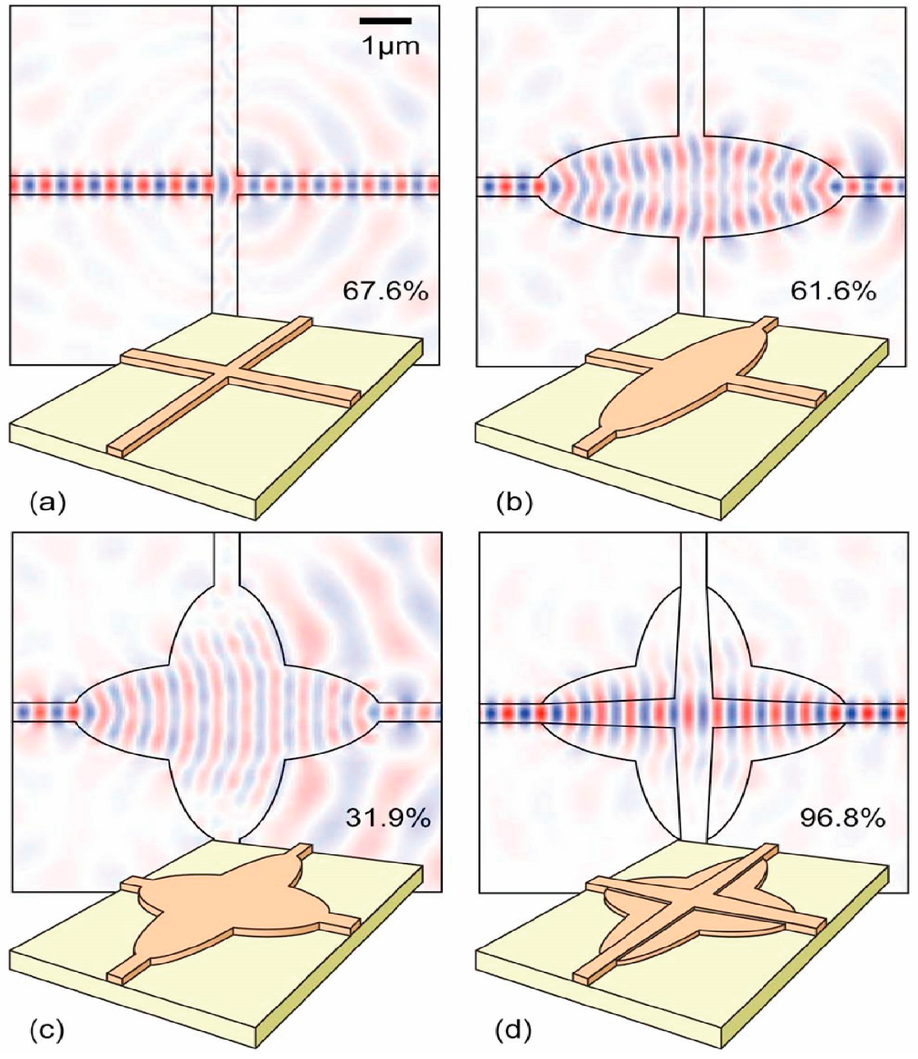
As illustrated in Figure 1, this physical process can be intuitively observed through 2-D FDTD optical field propagation simulations [46]. In the simple direct crossing shown in Figure 1a, the optical beam severely spills over in the central region, resulting in a low transmittance of only 67.6%. When the diverged beam reaches the opposing output waveguide port, its mode spot size is typically already significantly larger than the receiving aperture of the output waveguide. Such mode profile mismatch prevents a substantial portion of the optical energy from recoupling into the fundamental mode. Instead, the energy excites radiation modes or scatters into the substrate and cladding, culminating in irreversible scattering loss [47]. Both computational and experimental results indicate that the loss per single simple direct crossing in the 1550 nm band typically ranges from 1.1 to 1.4 dB [46,48]. This magnitude of loss is entirely unacceptable for large-scale PICs, which often necessitate the cascading of hundreds or thousands of such crossings. In contrast, widening the waveguides in conjunction with a double-etching technique to lower the local refractive index contrast (Figure 1d) can effectively maintain optical field confinement and suppress diffraction, thereby significantly reducing the loss.

2.1.2. Crosstalk Mechanisms

Crosstalk refers to the phenomenon where optical signals unintentionally couple from the input port to orthogonal waveguide ports. In direct crossings, crosstalk is primarily induced by the following two mechanisms:
Direct Scattering Coupling: As the beam diffracts and expands within the crossing region, a portion of the optical energy “overflows” and is captured by waveguides in the orthogonal direction. This non-resonant broadband scattering constitutes the primary source of background crosstalk.
Interface Reflection: Due to the discontinuity of waveguide sidewalls, Fresnel reflection occurs when light enters and exits the crossing region interfaces. Although the reflectivity of individual interfaces is relatively low, at specific wavelengths, reflected light may couple into the backward transmission modes of orthogonal waveguides.
Generally, the crosstalk level of simple direct crossings ranges from −30 dB to −10 dB, depending on the crossing angle and waveguide dimensions [24]. While crosstalk of −20 dB is typically acceptable for digital signals, such levels of background noise will severely degrade the signal-to-noise ratio and quantum state purity in analog optical computing or quantum photonics applications.

2.2. Design Based on Multimode Interference

To overcome the severe diffraction loss inherent in direct crossings, waveguide crossing designs based on the MMI principle have emerged as a widely adopted solution. The core operating mechanism of an MMI crossing is the self-imaging effect. When the fundamental mode optical field from a single-mode waveguide is injected into a wider multimode waveguide region, a series of higher-order modes are excited. Due to their different phase constants, these modes interfere with each other during propagation. According to the classical theory by Soldano et al. [49], at specific propagation distances (i.e., self-imaging lengths), these dispersed modes undergo constructive interference, refocusing and reconstructing an “image” of the input optical field at the output port. In crossing applications, the MMI region is typically designed as a 1 × 1 self-imaging structure; its physical advantages lie in reduced sidewall scattering and improved fabrication tolerance [50].
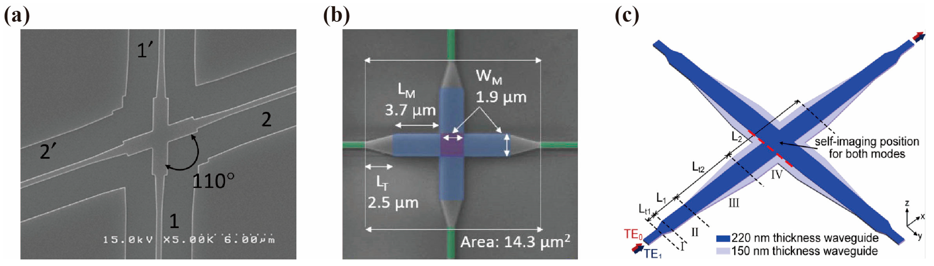
To suppress crosstalk and optimize polarization characteristics, researchers have introduced geometric innovations based on traditional orthogonal MMI structures. Kim et al. proposed a tilted MMI crossing scheme [51], as shown in Figure 2a. By optimizing the intersection angle between the two intersecting MMI waveguides, this design effectively alters the distribution of scattered light within the intersection region, thereby minimizing the light coupled into the orthogonal ports. Furthermore, through polarization diversity circuit design, it can simultaneously support the efficient transmission of both TE and TM polarization mode, providing robust support for the construction of polarization diversity systems.
Recent studies indicate that parameter-optimized MMI crossings can achieve exceptional performance metrics. For instance, Johnson et al. demonstrated a compact MMI crossing based on a standard SOI platform, as depicted in Figure 2b. Experimental measurements reveal that this device achieves an ultra-low insertion loss of only 0.043 dB per crossing and an inter-channel crosstalk below −50 dB within the 1550–1560 nm range [52]. Moreover, this study quantified the backscattering of the crossing in the frequency domain for the first time, yielding a measured value as low as −55 dB. This result is crucial, as ultra-low backscattering is a key factor in ensuring system stability in quantum photonic circuits or high-precision interferometric systems.
Another significant improvement strategy involves the adoption of a shallow-etched step structure. Wu et al. proposed a novel MMI crossing that combines full-etch and shallow-etch processes [53], as shown in Figure 2c. By introducing a 70-nm-deep shallow-etched layer within the MMI multimode region, the researchers successfully tailored the effective refractive indices of the fundamental mode (TE0) and the higher-order mode (TE1), respectively. This “dispersion engineering” enables the precise coincidence of the self-imaging positions for different modes, thereby resolving the issue of self-imaging position shifts during multimode transmission.

2.3. Design Based on Mode Evolution

In contrast to MMI structures that utilize multimode interference effects, designs based on mode evolution aim to directly alter the propagation behavior of the optical field by manipulating the waveguide geometry or the refractive index distribution of the material. The core strategies are categorized into two types: first, reducing the diffraction divergence angle through adiabatic or quasi-adiabatic mode spot expansion; second, constructing gradient-index (GRIN) lenses using transformation optics principles to achieve spatial mapping of optical paths.

2.3.1. Adiabatic Mode Spot Expanders

The most intuitive approach to mitigate scattering loss in waveguide crossings is to enlarge the mode field size. According to Gaussian beam theory, the Rayleigh length of an optical beam is proportional to the square of its waist radius. By adiabatically expanding the waveguide mode into a broadened beam, its collimated propagation distance can be significantly extended, allowing it to effortlessly traverse the intersection region without the need for complex focusing structures [54].
Conventional long linear tapers, while exhibiting excellent adiabaticity, suffer from excessively large footprints. To resolve this trade-off, Chen et al. proposed a cascaded multimode taper structure [55]. This design utilizes the eigenmode expansion (EME) method to optimize the profile of a three-section cascaded taper, effectively reducing the device length while maintaining adiabatic evolution. Numerical simulations indicate that this device achieves a low loss of 0.13 dB at a wavelength of 1550 nm, within a compact footprint of 4.16 × 4.16 μm2. In the pursuit of extreme compactness and enhanced fabrication tolerance, Chandran et al. introduced the concept of cosine beam shaping [56]. They designed an ultra-compact crossing measuring merely 4.7 × 4.7 μm2 on the GLOBALFOUNDRIES 45 nm CMOS platform. By optimizing the curvature of the cosine taper, this structure rapidly expands and reshapes the optical field into a diffraction-resistant focused beam, achieving a low loss of approximately 0.2 dB and a crosstalk below −35 dB across the O-band (1260–1360 nm).
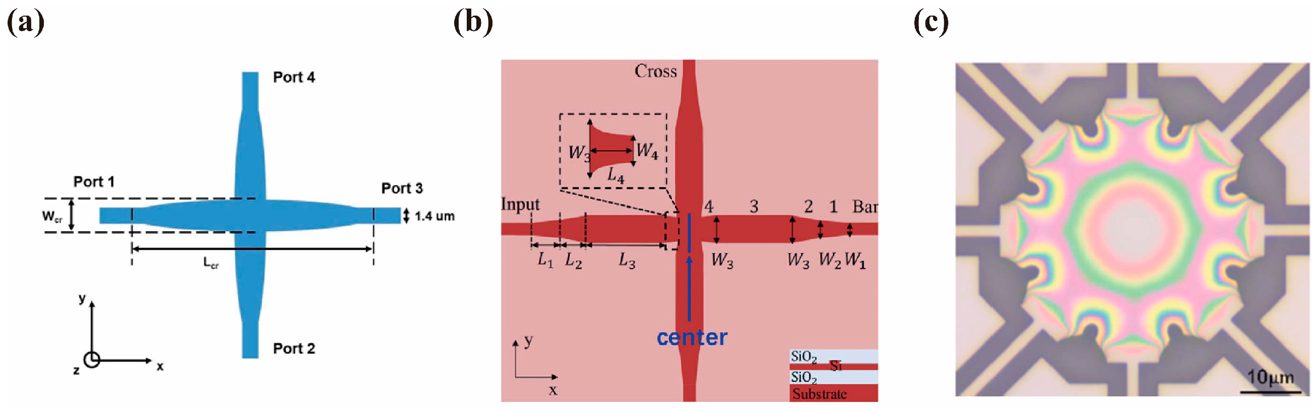
Based on a Gaussian beam synthesis method, Han et al. designed a waveguide crossing utilizing an elliptical parabolic inverse taper on the SOI platform [57], as shown in Figure 3a. This structure synthesizes a two-dimensional Gaussian beam at the center of the intersection to suppress scattering loss. Experimental measurements over a 40-nm bandwidth in the O-band revealed a crosstalk below −40 dB and an insertion loss as low as 0.008 dB (at 1321 nm), representing the lowest reported loss for silicon planar waveguide crossings in the O-band to date.
Paralleling the extensive research on SOI platforms, Lu et al. proposed an elliptical waveguide crossing on a silicon nitride platform to address the demands of high-density microwave photonic integration [58], as illustrated in Figure 3b. This design incorporates two mutually perpendicular elliptical taper waveguides within the crossing region, where the gradual curvature of the elliptical profile effectively mitigates the scattering loss typically associated with direct intersections. Experimental verification demonstrated an insertion loss of approximately 0.086 dB for this elliptical crossing. Furthermore, the loss variation is less than 0.02 dB across the entire 1540–1560 nm operating band, with both crosstalk and reflection remaining below −44 dB. These results thoroughly highlight the promising potential of low-loss crossings for large-scale on-chip microwave photonic processors.

2.3.2. Transformation Optics and Maxwell Fish-Eye Lenses

Transformation optics provides a highly versatile theoretical framework for optical field manipulation [59]. Through coordinate transformations, light trajectories can be “bent” and refocused within physical space, thereby establishing a scattering-free “invisibility” channel across the intersection region. Among various models, the Maxwell’s fish-eye lens is the most widely adopted due to its perfect imaging characteristics, which enable the aberration-free focusing of light from a source point to its conjugate point [60].
Badri et al. initially conducted a theoretical investigation into the feasibility of mapping a circular MFE lens into a square configuration [61]. By employing quasi-conformal transformation optics, a square GRIN lens was designed. This specific geometry seamlessly accommodates the Manhattan grid layout typical of PICs, theoretically resolving the wavefront and mode mismatch issues conventionally encountered when interfacing circular MFE lenses with straight waveguides. To further enhance fabrication compatibility, Badri et al. subsequently extended this concept to a silicon nitride platform, utilizing SWG metamaterials to achieve a gradient profile of the equivalent refractive index [62]. This all-dielectric, planar lens architecture effectively eliminates the requirement for complex three-dimensional (3D) topographies. Simulation results demonstrate that this SWG-based GRIN lens crossing exhibits a crosstalk below −29 dB and an average insertion loss of approximately 0.46 dB across the 1500–1600 nm wavelength range, occupying a compact footprint of merely 5.65 µm × 5.65 µm. Moreover, this design can be scaled to support multimode transmission by proportionally increasing the waveguide width and lens dimensions, substantiating the tremendous potential of transformation optics in multimode photonic routing.
Distinct from the square lens approach, Li et al. proposed a universal multimode waveguide star cross-junction based on strict conformal transformation optics, which in principle imposes no limitations on the number of modes and channels [34], as shown in Figure 3c. To resolve the wavefront and refractive index mismatches between circular Maxwell fisheye lenses and straight waveguides, they developed an artificial boundary conformal mapping (ABCM) method. By introducing an artificial boundary and locally compressing coordinates, the circular ports of the lens were reshaped into flat ports. Concurrently, the center-to-boundary refractive index ratio was precisely regulated from 2:1 to 1:1, making it fully compatible with the effective refractive index range (1.44–2.83) of a 220-nm-thick SOI slab waveguide. At 1550 nm, the designed four-channel, three-mode star cross-junction exhibited simulated transmission efficiencies of 99.5%, 97.7%, and 95.3% for theTE0, TE1, and TE2 modes, respectively, with crosstalk below −37 dB. The device was fabricated using grayscale electron-beam lithography, yielding measured transmission efficiencies of 87.3–53.9% for the TE0–TE2 modes and an inter-channel crosstalk below −40 dB. This work highlights the immense potential of transformation optics for achieving ultra-wideband, scalable multimode photonic routing.

2.4. Dielectric Engineering Based on Subwavelength Structures

The emergence of SWG has revolutionized the design paradigm of silicon photonic devices. By introducing micro-nano structures with periods far smaller than the operating wavelength into waveguides, SWGs can suppress diffraction effects and macroscopically behave as metamaterials with tunable equivalent refractive indices and artificial anisotropy. This “dielectric engineering” capability provides new physical degrees of freedom for addressing loss and crosstalk issues in crossings [63].

2.4.1. Artificial Anisotropy and Refractive Index Distribution Engineering

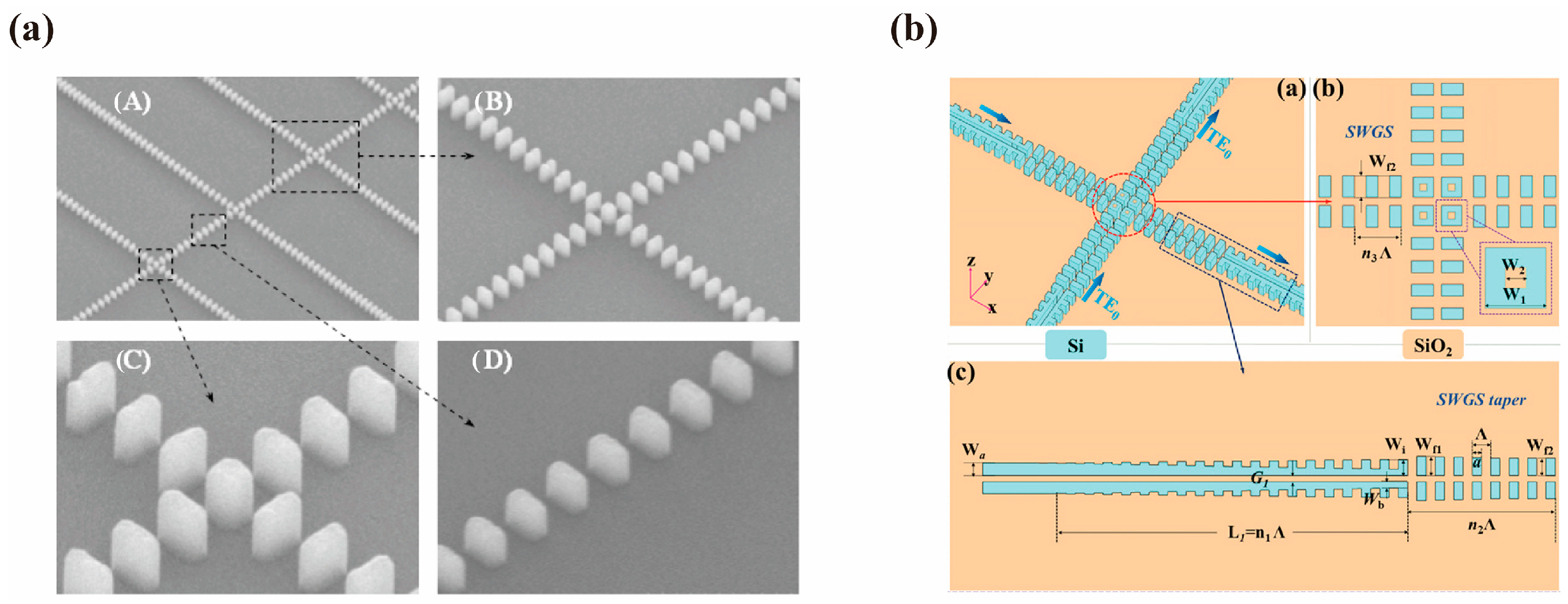
As early as 2010, Bock et al. pioneered the first silicon waveguide crossing based on SWGs by leveraging EMT [64], as shown in Figure 4a. They achieved adiabatic mode conversion by tapering the period and width of the SWG segments, which expands the mode profile of the optical field at the intersection, while successfully suppressing beam diffraction via subwavelength effects. Experimental results demonstrated that this structure achieves an insertion loss as low as 0.023 dB/crossing, an ultra-low crosstalk of less than −40 dB, and a polarization-dependent loss (PDL) below 0.02 dB. Being fully compatible with single-step etching processes, this work laid an early foundation for optimizing waveguide crossing performance using SWG structures. A critical challenge in conventional waveguide crossings is the loss of lateral optical field confinement at the intersection center. Leveraging the structural anisotropy of SWGs, transmission channels that are effectively “invisible” to specific polarizations can be constructed. Zhao et al. proposed a multimode crossing based on the hybrid anisotropy of 1D/2D SWGs [65]. Utilizing effective medium theory (EMT), they meticulously designed the 2D-SWG region at the intersection center and the 1D-SWG gratings in the connecting arms. This configuration ensures that the equivalent refractive index of the central region for TE-polarized light is higher than that of the lateral regions, thereby forming a straight-waveguide-like refractive index profile that physically suppresses diffraction loss. However, because SWG structures are inherently sensitive to fabrication tolerances such as etching depth and sidewall roughness, their stringent 50-nm manufacturing requirement and sole reliance on TE polarization represent major limitations to be overcome in large-scale photonic chip manufacturing.
Furthermore, SWGs have demonstrated robust adaptability for more complex polarization states and waveguide configurations. By optimizing the SWG duty cycle, Xu et al. constructed a gradient refractive index profile—high in the center and low on the sides—successfully realizing a broadband, polarization-insensitive crossing. Experimental results demonstrate that the device, with a compact footprint of 10.4 × 10.4 μm2, achieves high-efficiency transmission for both TE0 and TM0 modes over the wavelength range of 1500–1600 nm. However, it exhibits relatively high reflection loss under operational conditions [66].
Addressing the traditionally high-loss issue in slot waveguide crossings, Zhu et al. proposed employing an anisotropic SWG slot waveguide structure to suppress mode diffraction within the slot, paving the way for slot waveguide routing in applications such as high-sensitivity sensing [67], as illustrated in Figure 4b. As the first experimentally verified slot waveguide crossing, the optimized device achieved an insertion loss of ~0.1 dB and a crosstalk of <−35 dB within the 1500–1580 nm range (with simulations indicating an ultra-broadband performance spanning 576 nm), supporting exclusively TE-mode transmission.
Figure 4. On-chip waveguide crossing based on subwavelength structures: (a) scanning electron microscope images of SWG crossings, where (A–D) represent multiple SWG crossings, one SWG crossing, detail of the crossing region, and SWG straight waveguide [64], and (b) 3D schematic diagram of the crossing, where (a–c) show 3D schematic diagram of the crossing, top view of the central crossing section, and top view of the mode converter section [67].
Photonics 13 00539 g004

2.4.2. Subwavelength Transmitarray (SWTAs) and Bound States in the Continuum Mechanisms

Beyond serving as an equivalent medium, SWGs can also be engineered as phase modulation units, known as subwavelength transmitarrays. Guo et al. introduced a novel SWTA-based mechanism that utilizes asymmetric slot structures to form bound states within the intersection region [68]. Distinct from conventional total internal reflection, this mechanism “locks” light along its propagation path via a refractive index potential well, thereby suppressing leakage in the orthogonal direction. A three-mode crossing fabricated based on this principle features a compact footprint of merely 5.05 × 5.05 µm2 and exhibits exceptional ultra-broadband characteristics (1.4–2.1 µm, yielding a 700-nm bandwidth). Simulations indicate an insertion loss of <0.77 dB and a crosstalk of <−30 dB. Furthermore, it is scalable up to ten-mode transmission, spanning the near-infrared to short-wave infrared bands.
In pursuit of ultimate bandwidth and scalability, Gao et al. recently proposed and experimentally demonstrated an ultra-broadband, dual-polarization waveguide crossing architecture [69]. By employing a composite SWG structure combined with unified MMI motifs, this design compresses the footprint of a 2 × 2 configuration in the ITU bands down to 14 × 14 μm2. Additionally, it achieves low-loss, low-crosstalk, and non-blocking transmission that covers the O-to-L communication bands and extends into the 2 μm mid-infrared regime. This versatile and scalable SWG-based architecture robustly validates its fundamental application value for future multi-band, multi-polarization on-chip optical networks. Its primary drawback lies in a slight compromise in TM-mode performance under high-density port configurations, and the 4 × 4 structure requires minor dummy fillings at the corners to ensure fabrication feasibility.

2.5. Algorithm-Driven Inverse Design

With the exponential growth in the density of PICs, traditional design methods based on physical intuition (such as MMI or tapered waveguides) are gradually reaching their bottlenecks when addressing the demands for multimode, multi-polarization, and ultra-compact footprints. Algorithm-driven inverse design discretizes the functional regions of a device into subwavelength pixels or freeform curves. By employing algorithms such as topology optimization, direct binary search (DBS), and gradient descent, it searches for non-intuitive optimal solutions within a vast parameter space [70]. This approach not only breaks through the inherent trade-off between footprint and performance but also endows devices with unique functionalities unattainable by conventional geometric structures [71].
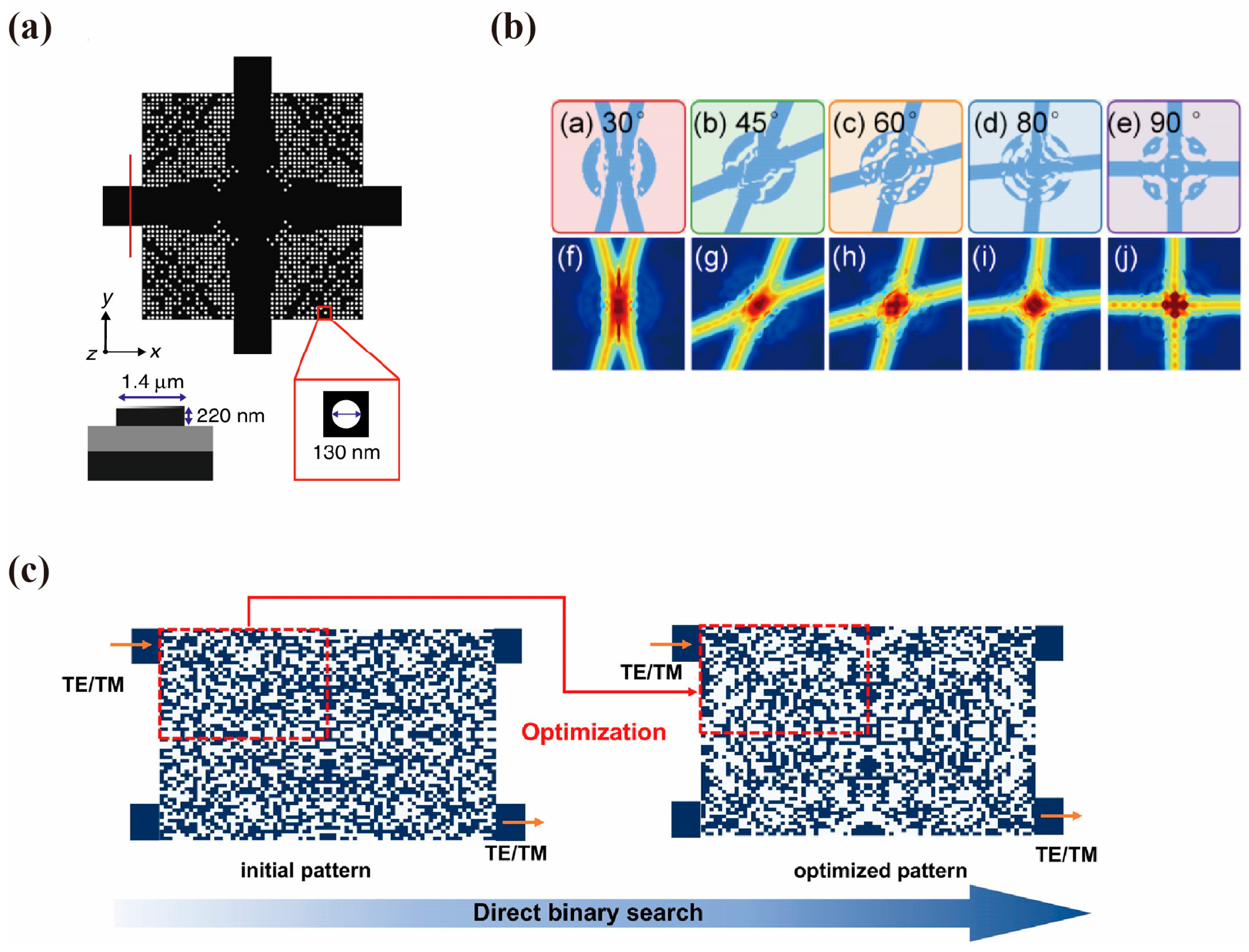
The initial breakthrough of inverse design lies in its ability to overcome the geometric constraints of Manhattan routing. Liu et al. pioneered the concept of “digital metamaterials,” utilizing computer-generated pixelated patterns (with a minimum feature size of 130 nm) to precisely modulate the optical field phase [72], as shown in Figure 5a. Their experimentally demonstrated three-mode MDM circuit not only supports arbitrary routing paths but also achieves high-speed signal transmission of 112 Gbit/s within an extremely compact footprint. The bit error rate is below the 20% forward error correction limit, proving the exceptional performance of the irregular structures generated by inverse design under standard silicon photonics processes. Although the 130-nm minimum pixel size used in this design is feasible for laboratory electron-beam lithography, it represents a fine node for large-scale deep-ultraviolet (DUV) lithography, imposing stringent requirements on overlay accuracy and etching uniformity. Subsequently, addressing the demand for flexibility in non-orthogonal routing, Dong et al. utilized the finite-difference frequency-domain (FDFD) method combined with a global optimization algorithm to design an X-shaped crossing with an arbitrary intersection angle [73], as depicted in Figure 5b. This design breaks the limitations of traditional 90° crossings, realizing flexible intersection angles such as 30°, 45°, 60°, 80°, and 90° (supporting only the TE0 mode), with a device footprint of only 4.5 µm2 (a circular region with a radius of 1.2 µm). Such geometric degrees of freedom significantly optimize the layout utilization of the chip and reduce the losses induced by unnecessary waveguide bends. However, while performance is optimized for the 1525–1575 nm, this inversely designed structure exhibits strong wavelength selectivity; its performance degrades rapidly away from the design wavelengths, contrasting with broadband MMI- or SWG-based structures.
In system-level applications, inverse design exhibits outstanding customized design capabilities and integration potential. Addressing the pain points in large-scale optical switch matrices (such as the Benes network)—where the cascading of traditional 2 × 2 waveguide crossings requires numerous connecting waveguides, easily leading to cumulative losses and large layout areas—Ma et al. realized a 6 × 6 waveguide crossing specifically designed for the Benes network via inverse design [74]. Within an ultra-compact footprint of 9 µm × 6.72 µm, this device achieves low-insertion-loss and low-crosstalk directional transmission from 6 input ports to 6 output ports. Compared to the conventional scheme of cascading multiple 2 × 2 crossings, this “all-in-one” customized design significantly simplifies the topology of the Benes network, substantially reducing the cumulative loss of the system while effectively shrinking the overall layout area of the network. However, although simulations indicated a certain fabrication tolerance (with a diameter variation of ± 10 nm), the measured loss of 1.8 dB was noticeably inferior to the simulated value of <0.7 dB, which is mainly attributed to fabrication-induced sidewall roughness, etching non-uniformity, and the non-uniform of reference grating couplers.
Figure 5. On-chip waveguide crossings based on inverse design: (a) a digital metastructure waveguide crossing, where the red box in Figure 4a is a magnified view of the unit cell, with a hole diameter of 130 nm [72], (b) an X-shaped waveguide crossing with an arbitrary intersection angle, where (a–e) show the simulation results of the optimized structures (designed for TE0 mode) and (f–j) the corresponding electric field distributions [73], and (c) a waveguide crossing designed via a deep-learning-assisted hybrid global optimization strategy, where the red dashed boxes depict the initial and optimized areas, the orange arrows show the input and output ports for TE/TM mode, and the red arrow illustrates the optimization from initial to optimized pattern [75].
Photonics 13 00539 g005
In recent years, the evolution of the algorithms themselves has elevated device performance to unprecedented heights. To resolve the dilemma of balancing polarization sensitivity with optimization efficiency, Wang et al. introduced a DBS strategy with mirror-symmetry constraints [75], as shown in Figure 5c. By applying X/Y-axis symmetry constraints, this method compresses the search space from 4800 pixels to 1200 pixels, remarkably enhancing optimization efficiency and successfully generating a crossing that features both ultra-low loss and high polarization robustness. Simulation results demonstrate that the device achieves an ultra-compact footprint of 3 × 4 μm2 on a 340-nm-thick SOI platform, with insertion loss below 0.11 dB (TE0)/0.05 dB (TM0) and crosstalk below −22.6 dB/−24.5 dB across the C-band. While the thicker silicon layer facilitates multimode and polarization-insensitive design, its compatibility with industry-standard 220-nm SOI foundry processes is slightly reduced compared to mainstream platforms, presenting a trade-off between optical functionality and manufacturing scalability.
In terms of footprint scaling, Liu et al. combined inverse design with dielectric metasurface principles, compressing the size of a dual polarization crossing down to an astonishing 4.8 × 4.8 µm2 [76]. Simulation results indicate that the device possesses an ultra-broad operating bandwidth of 1200–1700 nm (covering the O- to U-bands), maintaining an insertion loss generally below 0.4 dB (TE0 < 0.45 dB, TM0 < 0.39 dB) and a crosstalk below −28 dB. Experimental measurements validated a low insertion loss (TE0 < 0.4 dB, TM0 < 0.7 dB) and low crosstalk (<−20 dB) within the 1500–1600 nm. Such “compact footprint, broad bandwidth” characteristics make it an ideal candidate for next-generation ultra-high-density optical interconnection architectures.

2.6. Core Physical Trade-Offs and Practical Manufacturability

To provide a more intuitive and systematic comparison of the overall performance of various silicon waveguide crossings, Table 1 summarizes the key performance metrics across different design paradigms, including MMI, adiabatic mode evolution, SWG, and inverse design. However, when evaluating the practical viability of these technologies for future high-density on-chip PICs, the assessment must extend beyond ideal performance upper bounds. A deeper analysis is required to scrutinize their underlying physical trade-offs as well as the mass-production bottlenecks encountered within realistic, standard CMOS foundry lines.
The evolutionary trajectory of high-performance silicon photonic waveguide crossings clearly illustrates a profound paradigm shift: from intuition-based forward construction to algorithm-driven inverse optimization, and from macroscopic geometric shaping to microscopic dielectric engineering. Concurrently, distinct physical trade-offs emerge among these paradigms across multiple performance metrics, including footprint, operating bandwidth, insertion loss, multidimensional functionality, and fabrication tolerance. The conventional MMI scheme inherently relies on the self-imaging effect within the multimode region. Featuring regular structures and moderate fabrication robustness, it effectively focuses the optical field to suppress scattering losses at the central intersection. However, its underlying physics strictly ties the geometry of the multimode region to specific interference phases, which limits the operating bandwidth and exponentially escalates design complexity when handling multi-mode or dual-polarization crossings due to intricate phase-matching conditions. To circumvent the constraints of interference phases, mode-evolution-based designs introduce an adiabatic tapering mechanism. By macroscopically sacrificing spatial dimensions (typically extending tens of micrometers) to achieve a gradual, lossless expansion of the mode spot, this approach significantly reduces the diffraction divergence angle within the unconstrained intersection, thereby delivering exceptional ultra-broadband and low-reflection characteristics. Nevertheless, such a bulky physical footprint exhibits an irreconcilable intrinsic contradiction with the ultra-high integration density demanded by modern high-performance PICs [10].
To break the inherent trade-off between macroscopic size and performance, SWG-based dielectric engineering balances structural layout degrees of freedom against the fabrication minimum feature size (MFS) by introducing micro-nano arrays with periodicities far below the operating wavelength. Utilizing effective medium theory to tailor intrinsic artificial anisotropy and gradient refractive indices, this strategy substantially compresses device footprints while sustaining excellent broadband and low-crosstalk characteristics. However, most conventional SWG schemes remain confined to regular periods or duty cycles, leaving their analytical frameworks struggling to address the extremely complex, non-local multiple scattering manipulation required for multi-mode and dual-polarization scenarios [64]. In contrast, algorithm-driven inverse design completely liberates device development from the constraints of human physical intuition. By pixelating the functional region or performing free-boundary topology optimization, it navigates deep trade-offs within a vast, multidimensional, non-linear solution space against high computational costs and fabrication distortions. This methodology successfully scales the physical footprint of waveguide crossings to its limit (down to the 2 μm × 2 μm scale) and has emerged as the most powerful tool for addressing multi-objective optimization targets—such as multi-mode and dual-polarization capabilities—that remain elusive for traditional methods. Nonetheless, its heavy reliance on computationally intensive adjoint simulations, alongside the extreme sensitivity of the resulting non-intuitive micro-nano structures to lithographic distortions and sidewall roughness, remains the primary physical bottleneck hindering high-yield industrial fabrication [70].
Although numerical simulations demonstrate highly promising theoretical capabilities for SWG, inversely designed, and metastructure-based crossings in terms of electromagnetic response, ultimate footprint scaling, and multi-mode/dual-polarization compatibility, a non-negligible chasm persists between idealized electromagnetic performance and actual physical manufacturing when transitioning to commercial CMOS foundry lines for mass production. Because these designs typically rely on extremely fine subwavelength pixels, intricate topological geometries, or aperiodic micro-nano arrays, they exhibit exceptional sensitivity to CMOS fabrication tolerances in modern semiconductor foundries [70]. In practical DUV lithography and high-precision dry etching processes, minute deviations in critical dimension (CD), alongside line edge roughness (LER) and inevitable sidewall roughness, can easily induce severe localized microscopic scattering losses and phase distortions. Consequently, the core performance metrics of fabricated devices, such as insertion loss and crosstalk, suffer severe degradation compared to numerical predictions [77].
Furthermore, ubiquitous phenomena during nanostructure patterning, such as corner rounding and etch lag, not only disrupt the delicate intrinsic phase responses of microscopic scatterers but also trigger multi-dimensional performance distortions when cascaded across large-scale on-chip networks, leading to a drastic decline in the overall chip yield. This extreme vulnerability to microscopic fabrication imperfections prevents these complex designs from seamlessly inheriting the excellent industrial scalability characteristic of traditional, intuition-based devices. This limitation has propelled a shift in current research focus: rather than merely chasing the ultimate performance in simulated parameters, contemporary efforts are entering a new phase of design for manufacturability (DFM), which inherently integrates stringent foundry design rule checks (DRC) and fabrication robustness constraints directly into the underlying optimization algorithms [70,77].

3. Functional Crossings for Multi-Dimensional Multiplexing

To meet the urgent demand for ultra-high data throughput in optical interconnect systems of the post-Moore era, merely increasing the number of single-mode waveguide ports is insufficient to support exponential capacity growth. Therefore, multiplexing using different physical dimensions of light—such as polarization states and spatial modes—has become a key technology for enhancing single-wavelength communication capacity [78]. In these complex interconnect networks, crossings must not only achieve low-loss basic routing functions but also possess the capability to simultaneously process multi-dimensional multiplexed signals. Table 2 summarizes the key performance metrics of silicon waveguide crossing designs employing multiplexing techniques, the detailed characteristics of which will be discussed in the following paragraphs.

3.1. Polarization-Division Multiplexing Crossings

PDM technology can directly double the capacity of communication links by simultaneously transmitting two orthogonal polarization states, TE and TM, within the same waveguide. However, on the SOI platform, due to the extremely high geometric birefringence of the waveguide structure, the TE and TM polarizations exhibit significant differences in their effective refractive indices and mode field distributions [90]. Consequently, conventional crossings are typically optimized for only a single polarization state (usually the TE mode), while the other polarization state suffers from severe scattering loss and crosstalk. Therefore, designing a polarization-insensitive crossing that accommodates both polarization states remains a formidable challenge.
Early dual-polarization crossings primarily relied on precisely optimized MMI structures. Chen and Shi proposed a polarization-insensitive crossing based on orthogonal MMI couplers on a standard platform [79]. By meticulously tuning the width and length of the MMI region, both TE and TM polarizations can achieve high-quality self-imaging within this area. Experimental results demonstrate that the device achieves low insertion loss and crosstalk for both TE and TM modes over the wavelength range of 1520–1610 nm. However, constrained by the inherent interference length of MMI, the device footprint remains relatively large at 23 × 23 μm2, which hinders high-density photonic integration compared to ultra-compact alternatives.
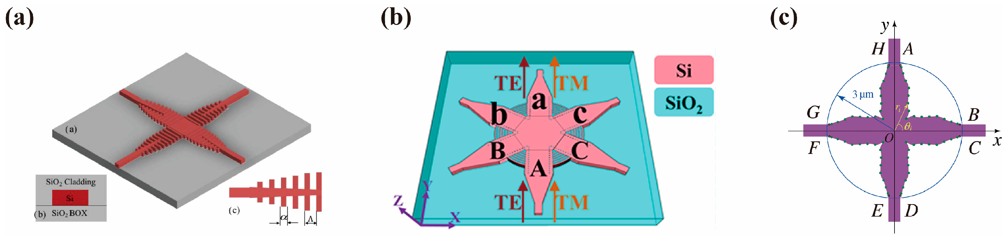
To overcome the footprint bottleneck and broaden the operational bandwidth, researchers began introducing SWGs into the design of dual-polarization devices. SWGs can effectively reduce the equivalent refractive index contrast of the waveguide, thereby mitigating the birefringence effect. Wu et al. demonstrated a compact polarization-insensitive crossing based on an SWG-assisted MMI [80], as depicted in Figure 6a. By introducing subwavelength pixels into the MMI region, they drastically reduced the device footprint to 12.5 × 12.5 µm2. Simulation results indicated insertion losses of approximately 0.46 dB and 0.64 dB for TE and TM polarizations, respectively, with a PDL < 0.2 dB and crosstalk below −35 dB. Experimental measurements over the C-band (1530–1565 nm) verified the low insertion loss (TE0 ~1.1 dB, TM0 ~1.6 dB) and low crosstalk (<−35 dB). With the increasing demand for complex network topologies, simple cross-shaped intersections can no longer satisfy all routing scenarios. Yu et al. further broke topological constraints and designed an ultra-compact polarization-insensitive 3 × 3 star-crossing using composite SWG metamaterials (nanopore gratings combined with fan-shaped bent SWGs) [81], as shown in Figure 6b. Within a hexagonal core region (measuring 12.68 × 10.98 µm2), this design achieved uniform, low-loss distribution of dual-polarization signals at various angles. Simulation results demonstrated an insertion loss < 0.2/0.3 dB (TE0/TM0) and crosstalk <−27.2/−23.6 dB in the 1500–1600 nm range; experimental validation in the C-band showed an insertion loss <0.35/0.4 dB and crosstalk <−31.5/−28.6 dB. This device provides a highly promising component for complex on-chip photonic matrices.
In recent years, with the maturation of inverse design algorithms, computer-generated dielectric metasurfaces have exhibited exceptional capabilities in manipulating multidimensional optical fields. Yu et al. pioneered the validation of inverse design advantages in addressing birefringent dispersion using greedy optimization and random walk methods, realizing a polarization-insensitive crossing that features both low loss and broadband characteristics [82], as illustrated in Figure 6c. Experimental characterization reveals that the device features a core design region with a radius of approximately 3 μm on the SOI platform, achieving insertion loss <0.2 dB and crosstalk <−28 dB across the broad wavelength range of 1440–1640 nm. This compact design demonstrates significant potential as a standardized building block for high-density photonic integrated circuits, balancing ultra-small footprint with robust optical performance.

3.2. Mode-Division Multiplexing Crossings

MDM technology can exponentially multiply interconnect capacity without increasing the number of laser wavelengths by utilizing multiple mutually orthogonal spatial physical modes (e.g., TE0, TE1, etc.) within the same waveguide as independent data channels. However, because modes of different orders possess starkly different effective refractive indices and mode field distributions (with higher-order modes exhibiting broader lateral distributions and a stronger tendency to diverge), simultaneously achieving self-imaging or beam collimation for all modes within a single physical intersection region is a highly challenging task. Conventional solutions often require demultiplexing higher-order modes into fundamental modes before crossing, and then multiplexing them again afterward. This not only drastically increases the device footprint (typically exceeding hundreds of micrometers) but also introduces additional cascade losses [34].
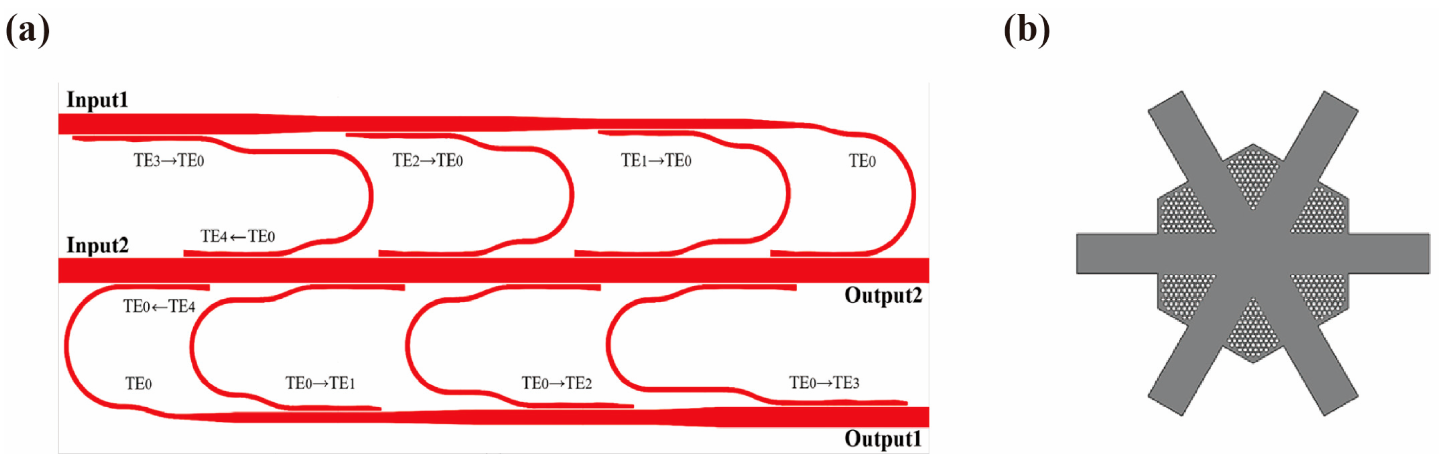
To realize the “direct” crossing of multimode signals, researchers initially focused on the footprint miniaturization and performance optimization of dual-mode devices. Using the adjoint shape optimization algorithm, Zhao et al. designed and experimentally verified an ultra-compact dual-mode crossing on a standard 220-nm SOI platform [83]. With a footprint of only 5 × 5 μm2, the device converged after just 18 iterations (6 h). Experimental results showed that at 1550 nm, the insertion losses for the TE0 and TE1 modes were as low as 0.83 dB and 0.50 dB, respectively. The inter-mode crosstalk was less than −20 dB (over an 80-nm bandwidth), and the device exhibited robust fabrication tolerance (±10 nm). Compared to traditional heuristic algorithms, this method boasts higher computational efficiency, yielding the optimal waveguide boundary profile within fewer iterations, thereby demonstrating the algorithm’s effectiveness in handling multimode phase matching. As system capacity increases, the number of modes that a crossing must support is evolving toward three or even four modes. To circumvent the severe interference that occurs when multiple modes intersect at the same physical point, Zhang et al. proposed a novel “parallel” silicon-based four-mode crossing scheme [84], as illustrated in Figure 7a. This device, with a footprint of 25 × 70 μm2, employs asymmetric directional couplers (ADCs) optimized via PSO. It utilizes an “idle” higher-order mode (TE4) in one waveguide as a relay to achieve the leapfrog routing of four modes (TE0–TE3) from another waveguide. Simulation results indicated an insertion loss < 0.5 dB and crosstalk <−20 dB within the 1530–1580 nm range. Rather than employing a traditional direct physical intersection, this scheme utilizes ADCs to realize leapfrog mode routing between two parallel main waveguides, offering excellent mode scalability (losses and crosstalk do not accumulate as the number of modes increases). Although this topology avoids direct scattering, achieving single-point direct crossing remains the ultimate pursuit for ultra-high-density integration as mode counts increase. To this end, spatial optical field manipulation based on metasurfaces and digital metastructures has shown immense potential. Liu et al. and Guo et al. demonstrated direct crossings supporting four spatial modes [85,86]. By utilizing computer-optimized digital metastructures (via the DBS algorithm) or phase-gradient slot arrays (with a 70-nm shallow etch), they simultaneously suppressed the divergence behaviors of four modes within extremely compact footprints (7.5 × 7.5 μm2 and 7.8 × 7.8 μm2). The insertion losses were maintained within 1 dB, with crosstalk <−18 dB and bandwidths spanning 80–200 nm.
In recent years, to further overcome the operational bandwidth and multi-channel interconnect limitations of MDM devices, researchers have introduced increasingly novel physical mechanisms and topological configurations. Regarding complex network topologies, Ma et al. utilized inverse design (the DBS algorithm) to break the traditional 2 × 2 orthogonal limitation, successfully developing highly symmetrical three-channel (a 4.32 × 4.32 μm2 regular hexagon) and four-channel (a 6.68 × 6.68 μm2 regular octagon) dual-mode crossings [91], as illustrated in Figure 7b. Experimental tests of this device recorded insertion losses < 1.8 dB (TE0) and < 2.5 dB (TE1), with crosstalk < −17.0 dB (1540–1560 nm), thereby greatly enriching the routing degrees of freedom for on-chip MDM networks.

3.3. Integration of Polarization Division Multiplexing and Mode Division Multiplexing

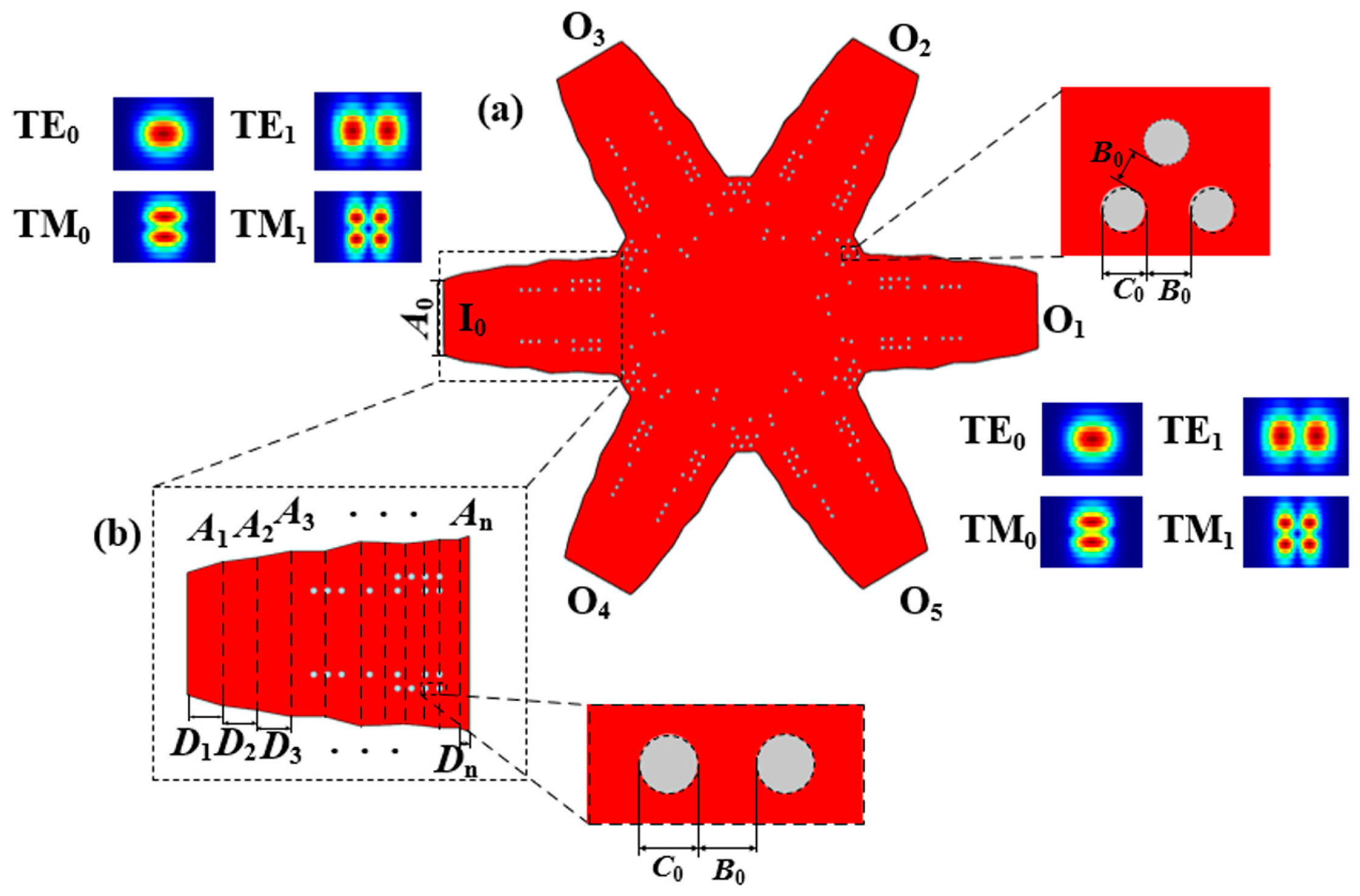
Recent trends indicate that the deep integration of PDM and MDM has become an inevitable path toward realizing universal photonic hubs. Zhang et al. demonstrated a crossing junction supporting dual polarizations and six spatial modes (TE0–TE2, TM0–TM2) by designing a digital dielectric meta-structure (nanohole pixel array) [87]. With a compact footprint of only 7.5 × 7.5 μm2, the device was optimized using a DBS algorithm. It achieved an insertion loss of < 1.2 dB (slightly higher for higher-order modes) and a crosstalk of <−13 dB over the 1460–1600 nm range, exhibiting good fabrication tolerance. This design provides a critical component for on-chip mode-division multiplexing systems. More recently, Ni et al. combined the PSO algorithm with DBS to create a “versatile” crossing junction featuring multi-channel, multi-mode, and polarization-insensitive capabilities within a mere 13.6 × 13.6 μm2 area [88], as shown in Figure 8a. This device supports 3-channel, 4-mode (TE0/TE1/TM0/TM1) transmission, with experimental tests demonstrating an insertion loss of < 1.8 dB and crosstalk of <−20.4 dB across the 1520–1600 nm band. In a highly visionary work, Liu et al. utilized an inverse-designed (via DBS algorithm) on-chip GRIN metalens to realize a universal multimode crossing junction [89]. Fabricated via a single-step full-etch process, the device supports flexible routing for three channels and enables efficient transmission for six modes (TE0–TE2 and TM0–TM2) simultaneously, achieving an experimental insertion loss of < 0.7 dB and crosstalk of <−14 dB in the 1500–1600 nm. This milestone achievement signifies that silicon-based waveguide crossing junctions have fully acquired the capability to manipulate full-dimensional optical parameters (multi-band, multi-polarization, multi-mode, and multi-channel). Furthermore, its scalability has been verified through five-channel dual-mode and 20-mode expansions. Collectively, these results demonstrate that algorithm-driven design can now effectively master the complex coupling boundaries of multidimensional optical parameters, laying a solid device foundation for future ultra-large-capacity on-chip interconnection networks.

4. Conclusions

This paper systematically reviews recent significant advances in multimode waveguide crossing technologies tailored for high-density integrated silicon photonic circuits. Addressing the severe challenges of diffraction scattering and inter-channel crosstalk inherent in traditional direct crossings, various efficient physical mechanisms and design paradigms have been proposed and validated. Among these, crossings based on Multimode Interference principles, leveraging their robust self-imaging characteristics, have achieved extremely low insertion loss and crosstalk within compact footprints, establishing themselves as a mature solution for constructing high-quality 2 × 2 multimode crossing components. Concurrently, designs grounded in Transformation Optics and Maxwell’s Fish-Eye lenses offer a novel physical perspective for eliminating scattering during optical field evolution, demonstrating immense potential for realizing high-order multimode crossings with ultra-low loss. Most notably, the convergence of SWG and algorithm-driven Inverse Design has fundamentally shattered the traditional trade-off boundaries between size and performance characteristic of heuristic designs. Experimental and simulation results indicate that SWG-based multimode crossings realized through inverse design not only deliver superior transmission performance but also significantly reduce device footprint compared to conventional waveguide components, exhibiting unprecedented ultra-compactness and degrees of freedom for multi-dimensional optical field manipulation.
Looking ahead, as optical interconnect systems evolve towards ultra-high throughput and complex network topologies, relying solely on passive, planar, and single-dimensional optimization will be insufficient to meet the extreme capacity demands of the post-Moore era. Future research on waveguide crossings and on-chip routing hubs is poised to transition from static component optimization towards system-level, multi-disciplinary integration. To transcend the limitations of conventional adjoint-method-based inverse designs, which are often computationally expensive and prone to local optima when handling multi-objective constraints, advanced deep learning architectures—such as generative adversarial networks (GANs) and physics-informed neural networks (PINNs)—are being introduced to enable ultra-fast, global-optimum, and tolerance-constrained generative design of complex multi-dimensional waveguide hubs [92]. Parallel to these algorithmic breakthroughs, augmenting pure silicon with heterogeneous material platforms offers a powerful pathway to overcome the platform’s inherent physical limits in broadband transparency and active tunability. By seamlessly integrating silicon photonics with low-loss silicon nitride, electro-optic polymers, or phase-change materials (PCMs), researchers can unlock novel capabilities such as non-volatile dynamic routing with zero static power consumption, thereby paving the way for ultra-low-power optical switching hubs [93].
At the network architecture level, the scaling of photonic integrated circuits into massive switching matrices and optical neural networks demands a parallel transition from static connectivity to dynamically reconfigurable nodes. Programmable photonics, powered by dense arrays of tunable interferometers arranged in topological meshes, can effectively transform rigid, passive waveguide crossings into flexible, software-defined optical hubs capable of self-healing and adaptive routing [94]. Ultimately, the most radical solution to the topological bottlenecks and in-plane scattering inherent to 2D planar intersections lies in the vertical dimension through 3D photonic integration. Utilizing multi-layer platforms, such as monolithic Si/SiN dual-layer integration, allows planar crossing hubs to be physically separated into different vertical planes and interconnected via ultra-low-loss interlayer transitions or optical vias. This 3D routing paradigm fundamentally bypasses planar intersections, radically suppressing inter-channel crosstalk and dramatically increasing the integration density of large-scale routing networks [95]. By embracing these converging advancements in intelligent design, material diversity, and architectural scalability, future full-dimensional photonic routing hubs will successfully solidify the core hardware foundation for next-generation on-chip optical interconnect systems that balance ultra-high integration density with rich functional versatility.

Author Contributions

B.N., J.C., Y.P., X.L., Q.Z., S.W. and J.X. contributed to the writing, reviewing and editing of this paper. All authors have read and agreed to the published version of the manuscript.

Funding

Fundamental Research Funds for the Central Universities (30924010911).

Data Availability Statement

Data underlying the results presented in this paper are not publicly available at this time but may be obtained from the authors upon reasonable request.

Conflicts of Interest

The authors declare no conflicts of interest.

References

  1. Zhong, K.; Zhou, X.; Huo, J.; Yu, C.; Lu, C.; Lau, A.P.T. Digital Signal Processing for Short-Reach Optical Communications: A Review of Current Technologies and Future Trends. J. Light. Technol. 2018, 36, 377–400. [Google Scholar] [CrossRef]
  2. Lin, L.; Zhong, Q.; Qiu, J.; Li, J.; Li, C.; Cheng, G. E-GRACL: An IoT Intrusion Detection System Based on Graph Neural Networks. J. Supercomput. 2025, 81, 42. [Google Scholar] [CrossRef]
  3. Waldrop, M.M. More Than Moore. Nature 2016, 530, 144–147. [Google Scholar] [CrossRef] [PubMed]
  4. Shekhar, S.; Bogaerts, W.; Chrostowski, L.; Bowers, J.E.; Anyanechi, K.C.; Kupferman, A.D.; Shiri, S.; Lo, S.M.; Soref, R.; Fainman, Y.; et al. Roadmapping the Next Generation of Silicon Photonics. Nat. Commun. 2024, 15, 751. [Google Scholar] [CrossRef]
  5. Doylend, J.K.; Knights, A.P. The Evolution of Silicon Photonics as an Enabling Technology for Optical Interconnection. Laser Photonics Rev. 2012, 6, 504–525. [Google Scholar] [CrossRef]
  6. Wang, D.; Nie, Y.; Hu, G.; Zhao, Y.; Liang, G.; Xu, Y.; Zhang, Z.; Chen, S.; Liu, J.; Wu, K.; et al. Ultrafast Silicon Photonic Reservoir Computing Engine Delivering over 200 TOPS. Nat. Commun. 2024, 15, 10841. [Google Scholar] [CrossRef]
  7. Zhou, H.; Dong, J.; Cheng, J.; Dong, W.; Shen, C.; Zhang, Y.; Gu, P.; Li, C.; Ni, H.; Ma, Z.; et al. Photonic Matrix Multiplication Lights up Photonic Accelerator and Beyond. Light Sci. Appl. 2022, 11, 30. [Google Scholar] [CrossRef]
  8. Yi, Y.; Wu, D.; Kakdarvishi, V.; Yu, B.; Zhuang, Y.; Khalilian, A. Photonic Integrated Circuits for an Optical Phased Array. Photonics 2024, 11, 243. [Google Scholar] [CrossRef]
  9. Liu, J.; Wu, Q.; Sui, X.; Li, L.; Cao, Z.; Shen, X.; Li, G.; Gu, Q.; Dai, Q. Research Progress in Optical Neural Networks: Theory, Applications and Developments. PhotoniX 2021, 2, 5. [Google Scholar] [CrossRef]
  10. Wu, S.; Mu, X.; Cheng, L.; Mao, S.; Fu, H.Y. State-of-the-Art and Perspectives on Silicon Waveguide Crossings: A Review. Micromachines 2020, 11, 326. [Google Scholar] [CrossRef]
  11. Zhao, Y.; Xiang, J.; He, Y.; Yin, Y.; He, A.; Zhang, Y.; Yang, Z.; Guo, X.; Su, Y. On-Chip Metamaterial Enabled Wavelength (De)Multiplexer. Laser Photonics Rev. 2022, 16, 2200005. [Google Scholar] [CrossRef]
  12. Zou, J.; Li, L.; Wang, C.; Zhuang, Y.; Wang, X.; Hu, J.; Luo, S.; He, J.-J. Novel High-Resolution and Large-Bandwidth Micro-Spectrometer Using Multi-Input Counter-Propagating Arrayed Waveguide Grating and Dual-Wavelength Grating Coupler on Silicon on Insulator. Laser Photonics Rev. 2023, 17, 2200355. [Google Scholar] [CrossRef]
  13. Wu, R.; Ding, F.; Li, F.; Liu, Y. Inverse-Designed Low-Crosstalk CWDM (De)Multiplexer Assisted by Photonic Crystals. J. Light. Technol. 2024, 42, 4899–4905. [Google Scholar] [CrossRef]
  14. Chen, Y.; Wang, P.; Fu, Q.; Sun, Y.; Zou, Y.; Dai, S.; Chen, W.; Chen, H.; Li, J.; Dai, T.; et al. Low-Loss and Low-Cross Talk Polarization-Insensitive Multimode Silicon Waveguide Crossing. Opt. Lett. 2024, 49, 4930–4933. [Google Scholar] [CrossRef]
  15. Chang, W.; Zhang, M. Silicon-Based Multimode Waveguide Crossings. J. Phys. Photonics 2020, 2, 022002. [Google Scholar] [CrossRef]
  16. Wang, Q.; He, Y.; Wang, H.; Wang, Z.; Shen, J.; Zhang, Y.; Su, Y. On-Chip Mode Division (De)Multiplexer for Multi-Band Operation. Opt. Express 2022, 30, 22779–22787. [Google Scholar] [CrossRef]
  17. Mao, S.; Cheng, L.; Zhao, C.; Wang, Y.; Li, Q.; Fu, H.Y. Compact Hybrid Five-Mode Multiplexer Based on Asymmetric Directional Couplers with Constant Bus Waveguide Width. Opt. Lett. 2023, 48, 2607–2610. [Google Scholar] [CrossRef] [PubMed]
  18. Wu, R.; Wang, X.; Qiao, X.; Wei, Y.; Liu, Y. Compact and Scalable Mode (De)multiplexer Using Inverse-designed Subwavelength Gratings. Opt. Express 2025, 33, 11541–11550. [Google Scholar] [CrossRef]
  19. Ruan, X.; Li, H.; Chu, T. Inverse-Designed Ultra-Compact Polarization Splitter–Rotator in Standard Silicon Photonic Platforms with Large Fabrication Tolerance. J. Light. Technol. 2022, 40, 7142–7149. [Google Scholar] [CrossRef]
  20. Ni, B.; Luo, C.; Xu, H.; Dai, Y.; Qian, Y.; Shen, Y.; Wu, S.; Xiong, J. Compact and Low-Crosstalk Multimode Waveguide Crossing Utilizing Subwavelength Holey Metamaterial Waveguides. Opt. Express 2024, 32, 35743–35754. [Google Scholar] [CrossRef] [PubMed]
  21. Hung, Y.-J.; Chen, C.-H.; Chung, H.-C.; Lai, J.-Z.; Tseng, S.-Y. Compact and Broadband Silicon Polarization Splitter–Rotator Using Adiabaticity Engineering. Opt. Lett. 2024, 49, 1852–1855. [Google Scholar] [CrossRef]
  22. Xu, Z.; Tu, B.; Liu, H. Ultra-High Extinction Ratio Polarization Beam Splitter Using an Antisymmetric Grating-Assisted Multimode Waveguide. Appl. Opt. 2024, 63, 5911–5916. [Google Scholar] [CrossRef]
  23. Xu, Z.; Tu, B.; Liu, H. High Performance TM-Pass Polarizer Using Multimode Bragg Grating Waveguide. Opt. Express 2024, 32, 13156–13165. [Google Scholar] [CrossRef]
  24. Chrostowski, L.; Hochberg, M. Silicon Photonics Design: From Devices to Systems; Cambridge University Press: Cambridge, UK, 2015; pp. 115–120. [Google Scholar]
  25. Shen, Y.; Harris, N.C.; Skirlo, S.; Prabhu, M.; Baehr-Jones, T.; Hochberg, M.; Sun, X.; Zhao, S.; Larochelle, H.; Englund, D. Deep Learning with Coherent Nanophotonic Circuits. Nat. Photonics 2017, 11, 441–446. [Google Scholar] [CrossRef]
  26. Dumais, P.; Goodwill, D.J.; Celo, D.; Jiang, J.; Bernier, E. Three-Mode Synthesis of Slab Gaussian Beam in Ultra-Low-Loss In-Plane Nanophotonic Silicon Waveguide Crossing. In Proceedings of the 2017 IEEE 14th International Conference on Group IV Photonics (GFP), Berlin, Germany, 1–3 March 2017; IEEE: New York, NY, USA, 2017; pp. 97–98. [Google Scholar]
  27. Zhang, Y.; Hosseini, A.; Xu, X.; Kwong, D.; Chen, R.T. Ultralow-Loss Silicon Waveguide Crossing Using Bloch Modes in Index-Engineered Cascaded Multimode-Interference Couplers. Opt. Lett. 2013, 38, 3608–3611. [Google Scholar] [CrossRef]
  28. Wu, B.; Yu, Y. Ultralow Loss Waveguide Crossing with Low Imbalance for Two Transverse Electric Modes. In Proceedings of the 2018 Asia Communications and Photonics Conference (ACP), Hangzhou, China, 26–29 October 2018; IEEE: New York, NY, USA, 2018; pp. 1–3. [Google Scholar]
  29. Chen, D.; Wang, L.; Zhang, Y.; Hu, X.; Xiao, X.; Yu, S. Ultralow Crosstalk and Loss CMOS Compatible Silicon Waveguide Star-Crossings with Arbitrary Included Angles. ACS Photonics 2018, 5, 4098–4103. [Google Scholar] [CrossRef]
  30. Nevlacsil, S.; Muellner, P.; Sagmeister, M.; Kraft, J.; Hainberger, R. Broadband Low Loss and Ultra-Low Crosstalk Waveguide Crossings Based on a Multimode Interferometer for 840 nm Operation. OSA Contin. 2020, 3, 334–343. [Google Scholar] [CrossRef]
  31. Xu, H.; Shi, Y. Dual-Mode Waveguide Crossing Utilizing Taper-Assisted Multimode-Interference Couplers. Opt. Lett. 2016, 41, 5381–5384. [Google Scholar] [CrossRef]
  32. Badri, S.H.; Saghai, H.R.; Soofi, H. Polygonal Maxwell’s Fisheye Lens via Transformation Optics as Multimode Waveguide Crossing. J. Opt. 2019, 21, 065102. [Google Scholar] [CrossRef]
  33. Xu, H.; Shi, Y. Metamaterial-Based Maxwell’s Fisheye Lens for Multimode Waveguide Crossing. Laser Photonics Rev. 2018, 12, 1800094. [Google Scholar] [CrossRef]
  34. Li, S.; Zhou, Y.; Dong, J.; Zhang, X.; Cassan, E.; Hou, J.; Yang, C.; Chen, S.; Gao, D.; Chen, H. Universal Multimode Waveguide Crossing Based on Transformation Optics. Optica 2018, 5, 1549–1556. [Google Scholar] [CrossRef]
  35. Lees, H.; Gao, W.; Withayachumnankul, W. All-Silicon, Low-Cross-Talk Terahertz Waveguide Crossing Based on Effective Medium. Opt. Lett. 2021, 46, 5469–5472. [Google Scholar] [CrossRef]
  36. Zhao, C.; Mao, S.; Cheng, L.; Wu, S.; Han, Y.; Li, Q.; Fu, H.Y. Compact Dual-Mode Waveguide Crossing Based on Subwavelength Gratings Assisted Multimode-Interference Couplers. In Proceedings of the 2021 26th Optoelectronics and Communications Conference (OECC), Hong Kong, China, 3–7 July 2021; IEEE: Piscataway, NJ, USA, 2021; pp. 1–3. [Google Scholar] [CrossRef]
  37. Ni, B.; Han, C.; Dai, Y.; Shen, Y.; Luo, C.; Qian, Y.; Wu, S.; Xiong, J. Design and Fabrication of Ultra-Compact, Low-Loss Waveguide Crossings Utilizing Subwavelength Perforated Metamaterial Waveguides. Opt. Express 2025, 33, 37267–37279. [Google Scholar] [CrossRef]
  38. Ni, B.; Xu, H.; Luo, C.; Wu, S.; Xiong, J. Low-Loss and Broadband Silicon-Based Multimode Waveguide Crossing at 2 μm Using 2-D Sub-Wavelength Holey Metamaterials. Opt. Express 2025, 33, 6788–6798. [Google Scholar] [CrossRef]
  39. Ni, B.; Luo, C.; Chen, H.; Wu, S.; Hou, L.; Liu, H.; Xiong, J. Compact and Broadband Dual-Polarization Waveguide Crossing Utilizing Subwavelength-Hole-Assisted MMI Couplers. Opt. Lett. 2023, 48, 6040–6043. [Google Scholar] [CrossRef]
  40. Gao, Z.; Zhang, C.; Feng, J.; Guo, Z.; Yao, X.S.; Wu, S. Ultra-broadband polarization-insensitive dual-mode silicon waveguide crossing enabled by subwavelength grating-array-assisted multimode engineering. Opt. Lett. 2026, 51, 333–336. [Google Scholar] [CrossRef]
  41. Han, H.-L.; Li, H.; Zhang, X.-P.; Liu, A.; Lin, T.-Y.; Chen, Z.; Lv, H.-B.; Lu, M.-H.; Liu, X.-P.; Chen, Y.-F. High Performance Ultra-Compact SOI Waveguide Crossing. Opt. Express 2018, 26, 25602–25611. [Google Scholar] [CrossRef]
  42. Yi, D.; Zhou, W.; Zhang, Y.; Tsang, H.K. Inverse Design of Multi-Band and Wideband Waveguide Crossings. Opt. Lett. 2021, 46, 884–887. [Google Scholar] [CrossRef]
  43. Wang, X.; Chen, Y.; Zhao, F.; Xue, M.; Li, H.; Wei, Y.; Zang, Z.; Liu, Y. Ultra-Broadband and Multi-Channel Polarization-Insensitive Multimode Waveguide Crossings. J. Light. Technol. 2025, 43, 9282–9289. [Google Scholar] [CrossRef]
  44. Lu, W.; Shi, H.; Ma, C.; Li, Z.; Zhu, S.; Wu, Y.; Tai, R. Ultra-Low Loss SOI Waveguide Crossings Designed by a Hybrid Global Optimization Based on Deep Learning. Opt. Commun. 2024, 556, 130189. [Google Scholar] [CrossRef]
  45. Chen, J.; Pan, W.; Ji, C. Ultra-Broadband Four-Mode Waveguide Crossing via Inverse Design Method. In Proceedings of the 2023 IEEE Photonics Conference (IPC), Orlando, FL, USA, 12–16 November 2023; IEEE: Piscataway, NJ, USA, 2023; pp. 1–2. [Google Scholar] [CrossRef]
  46. Bogaerts, W.; Dumon, P.; Van Thourhout, D.; Taillaert, D.; Jaenen, P.; Wouters, J.; Beckx, S.; Wiaux, V.; Baets, R. Low-Loss, Low-Crosstalk Crossings for Silicon-on-Insulator Nanophotonic Waveguides. Opt. Lett. 2007, 32, 2801–2803. [Google Scholar] [CrossRef]
  47. Fukazawa, T.; Hirano, T.; Ohno, F.; Baba, T. Low Loss Intersection of Si Photonic Wire Waveguides. Jpn. J. Appl. Phys. 2004, 43, 646–647. [Google Scholar] [CrossRef][Green Version]
  48. Sakai, A.; Fukazawa, T.; Baba, T. Low Loss Ultra-Small Branches in a Silicon Photonic Wire Waveguide. IEICE Trans. Electron. 2002, E85-C, 1033–1038. [Google Scholar]
  49. Soldano, L.B.; Pennings, E.C. Optical Multi-Mode Interference Devices Based on Self-Imaging: Principles and Applications. J. Light. Technol. 1995, 13, 615–627. [Google Scholar] [CrossRef]
  50. Besse, P.A.; Bachmann, M.; Melchior, H.; Soldano, L.B.; Smit, M.K. Optical Bandwidth and Fabrication Tolerances of Multimode Interference Couplers. J. Light. Technol. 1994, 12, 1004–1009. [Google Scholar] [CrossRef]
  51. Kim, S.H.; Cong, G.; Kawashima, H.; Hasama, T.; Ishikawa, H. Tilted MMI Crossings Based on Silicon Wire Waveguide. Opt. Express 2014, 22, 2545–2551. [Google Scholar] [CrossRef]
  52. Johnson, M.; Thompson, M.G.; Sahin, D. Low-Loss, Low-Crosstalk Waveguide Crossing for Scalable Integrated Silicon Photonics Applications. Opt. Express 2020, 28, 12498–12506. [Google Scholar] [CrossRef]
  53. Wu, B.; Yu, Y.; Zhang, X. Multimode Waveguide Crossing with Ultralow Loss and Low Imbalance. Opt. Express 2020, 28, 14705–14713. [Google Scholar] [CrossRef]
  54. Chen, H.; Poon, A.W. Low-loss multimode-interference-based crossings for silicon wire waveguides. IEEE Photonics Technol. Lett. 2006, 18, 2260–2262. [Google Scholar] [CrossRef]
  55. Chen, C.H. Compact Waveguide Crossings with a Cascaded Multimode Tapered Structure. Appl. Opt. 2015, 54, 828–832. [Google Scholar] [CrossRef]
  56. Chandran, S.; Dahlem, M.; Bian, Y.; Moreira, P.; Jacob, A.P.; Rakowski, M.; Stricker, A.; Nummy, K.; Meagher, C.; Peng, B.; et al. Beam Shaping for Ultra-Compact Waveguide Crossings on Monolithic Silicon Photonics Platform. Opt. Lett. 2020, 45, 6230–6233. [Google Scholar] [CrossRef]
  57. Lu, Z.; Li, J.; Chen, H.; Yang, S.; Chen, M. Low-Loss Waveguide Crossing for Complicated On-Chip Microwave Photonic Processor. IEEE Photonics J. 2024, 16, 5500505. [Google Scholar] [CrossRef]
  58. Han, L.; Ruan, X.; Tang, W.; Chu, T. Ultralow-loss waveguide crossing for photonic integrated circuits by using inverted tapers. Opt. Express 2022, 30, 6738–6750. [Google Scholar] [CrossRef] [PubMed]
  59. Leonhardt, U. Optical Conformal Mapping. Science 2006, 312, 1777–1780. [Google Scholar] [CrossRef]
  60. Leonhardt, U. Perfect Imaging without Negative Refraction. New J. Phys. 2009, 11, 093040. [Google Scholar] [CrossRef]
  61. Badri, S.H.; Saghai, H.R.; Soofi, H. Multimode Waveguide Crossing Based on a Square Maxwell’s Fisheye Lens. Appl. Opt. 2019, 58, 4647–4653. [Google Scholar] [CrossRef]
  62. Badri, S.H.; Gilarlue, M.M. Silicon Nitride Waveguide Devices Based on Gradient-Index Lenses Implemented by Subwavelength Silicon Grating Metamaterials. Appl. Opt. 2020, 59, 5269–5275. [Google Scholar] [CrossRef]
  63. Halir, R.; Bock, P.J.; Cheben, P.; Blanco-Redondo, A.; Alonso-Ramos, C.; Ashton, R.; Zaoui, W.S.; Schares, L.; Witzens, J.; Ortega-Moñux, A.; et al. Waveguide Sub-wavelength Structures: A Review of Principles and Applications. Laser Photonics Rev. 2015, 9, 25–49. [Google Scholar] [CrossRef]
  64. Bock, P.J.; Cheben, P.; Schmid, J.H.; Lapointe, J.; Delâge, A.; Xu, D.-X.; Janz, S.; Densmore, A.; Hall, T.J. Subwavelength grating crossings for silicon wire waveguides. Opt. Express 2010, 18, 16146–16155. [Google Scholar] [CrossRef] [PubMed]
  65. Zhao, W.; Yi, X.; Peng, Y.; Zhang, L.; Chen, H.; Dai, D. Silicon Multimode Waveguide Crossing Based on Anisotropic Subwavelength Gratings. Laser Photonics Rev. 2022, 16, 2100623. [Google Scholar] [CrossRef]
  66. Xu, Z. Broadband and Low Crosstalk Polarization-Insensitive Waveguide Crossing Using Subwavelength Structure. J. Light. Technol. 2025, 43, 4399–4403. [Google Scholar] [CrossRef]
  67. Zhu, J.; Yu, Q.; Jin, Y.; Huang, C.; Guo, Z.; Hao, P.; Xiao, J.; Wu, S. Compact and Low-Loss On-Chip Silicon Crossing Based on Subwavelength Grating Slot Waveguides. Opt. Express 2025, 33, 4902–4914. [Google Scholar] [CrossRef]
  68. Guo, X.; Wang, Z.; Zhang, Y.; Liu, Y.; Zhang, Z.; Xu, J.; Xiao, S.; Song, Q.; Xu, K. Ultra-Broadband Multimode Waveguide Crossing via Subwavelength Transmitarray with Bound State. Laser Photonics Rev. 2023, 17, 2200678. [Google Scholar] [CrossRef]
  69. Gao, Z.; Yu, Q.; Guo, Z.; Zhang, L.; Xiao, J.; Wu, S.; Yao, X.S. Ultra-Broadband Dual-Polarization Silicon Waveguide Crossing Architecture for Scalable Multi-Port Operation Across ITU and 2 µm MIR Bands. J. Light. Technol. 2025, 43, 9346–9358. [Google Scholar] [CrossRef]
  70. Molesky, S.; Lin, Z.; Piggott, A.Y.; Jin, W.; Vuckovic, J.; Rodriguez, A.W. Inverse Design in Nanophotonics. Nat. Photonics 2018, 12, 659–670. [Google Scholar] [CrossRef]
  71. Piggott, A.Y.; Lu, J.; Lagoudakis, K.G.; Petykiewicz, J.; Babinec, T.M.; Vuckovic, J. Inverse Design and Demonstration of a Compact and Broadband On-Chip Wavelength Demultiplexer. Nat. Photonics 2015, 9, 374–377. [Google Scholar] [CrossRef]
  72. Liu, Y.; Xu, K.; Wang, S.; Shen, W.; Xie, H.; Wang, Y.; Xiao, S.; Yao, Y.; Du, J.; He, Z.; et al. Arbitrarily Routed Mode-Division Multiplexed Photonic Circuits for Dense Integration. Nat. Commun. 2019, 10, 3263. [Google Scholar] [CrossRef]
  73. Dong, Z.; Qiu, J.; Chen, Y.; Fan, X.; Pang, K.; Zhang, H.; Yuan, X. Ultra-Compact X-Shaped Waveguide Crossings with Flexible Angles Based on Inverse Design. Opt. Express 2021, 29, 19715–19723. [Google Scholar] [CrossRef]
  74. Ma, H.; Yang, J.; Zhang, Z.; Wang, X.; Li, Y.; Liu, D. Inverse-designed 6 × 6 waveguide crossing for a Benes-based network. Opt. Express 2024, 32, 42908–42916. [Google Scholar] [CrossRef]
  75. Wang, L.; Zhou, H.; Shi, H.; Wang, X.; Li, Y.; Liu, D. Ultra-low Loss and Ultra-compact Polarization-insensitive SOI Multimode Waveguide Crossing Based on an Inverse Design Method. Photonics 2024, 11, 1137. [Google Scholar] [CrossRef]
  76. Liu, B.; Wan, Y.; Liu, Y. Ultracompact Polarization-Insensitive Waveguide Crossing Based on Dielectric Metasurface. IEEE Photonics Technol. Lett. 2024, 36, 39–42. [Google Scholar] [CrossRef]
  77. Piggott, A.Y.; Petykiewicz, J.; Su, L.; Vučković, J. Fabrication-Constrained Nanophotonic Inverse Design. Sci. Rep. 2017, 7, 1786. [Google Scholar] [CrossRef]
  78. Dai, D.; Bowers, J.E. Silicon-Based On-Chip Multiplexing Technologies and Devices for Peta-Bit Optical Interconnects. Nanophotonics 2014, 3, 283–311. [Google Scholar] [CrossRef]
  79. Chen, J.; Shi, Y. Polarization-insensitive silicon waveguide crossing based on multimode interference couplers. Opt. Lett. 2018, 43, 5961–5964. [Google Scholar] [CrossRef]
  80. Wu, S.; Mao, S.; Zhou, L.; Liu, L.; Chen, Y.; Mu, X.; Cheng, L.; Chen, Z.; Tu, X.; Fu, H.Y. A compact and polarization-insensitive silicon waveguide crossing based on subwavelength grating MMI couplers. Opt. Express 2020, 28, 27268–27276. [Google Scholar] [CrossRef]
  81. Yu, Q.; Guo, Z.; Zhu, J.; Zhang, L.; Hao, P.; Xiao, J.; Feng, T.; Wu, S. Ultra-Compact and Polarization-Insensitive Silicon Waveguide 3 × 3 Star-Crossing Based on Composite Subwavelength Grating Metamaterials. Opt. Lett. 2024, 49, 4326–4329. [Google Scholar] [CrossRef] [PubMed]
  82. Yu, Z.; Feng, A.; Xi, X.; Sun, X. Inverse-Designed Low-Loss and Wideband Polarization-Insensitive Silicon Waveguide Crossing. Opt. Lett. 2019, 44, 77–80. [Google Scholar] [CrossRef] [PubMed]
  83. Zhao, C.; Cheng, L.; Chen, H.; Mao, S.; Wang, Y.; Li, Q.; Fu, H.Y. Compact Dual-Mode Waveguide Crossing Based on Adjoint Shape Optimization. Opt. Lett. 2023, 48, 3873–3876. [Google Scholar] [CrossRef] [PubMed]
  84. Zhang, R.; Sun, S.; Zhang, F.; Chen, K.; Liu, L.; Zhu, N. Four-Mode Parallel Silicon Multimode Waveguide Crossing Scheme Based on the Asymmetric Directional Couplers. Opt. Express 2022, 30, 22442–22451. [Google Scholar] [CrossRef]
  85. Liu, Y.; Zhong, Z.; Wang, S.; Liu, Y.; Yao, Y.; Du, J.; Song, Q.; Xu, K. Four-Mode Waveguide Crossing via Digitized Meta-Structure. In Proceedings of the Optical Fiber Communication Conference (OFC), Washington, DC, USA, 6–10 June 2021; Paper F2B.3; Optica Publishing Group: Washington, DC, USA, 2021. [Google Scholar] [CrossRef]
  86. Guo, X.; Liu, Y.; Xu, K. Four-Modes Waveguide Crossing Utilizing Phase-Gradient Slot Array. In Proceedings of the 26th Optoelectronics and Communications Conference (OECC), Hong Kong, China, 3–7 July 2021; Paper M3D.4; IEEE: Piscataway, NJ, USA, 2021. [Google Scholar]
  87. Zhang, Z.; Liu, Y.; Xu, K. Dual-Polarization and Six-Mode Waveguide Crossing Based on Dielectric Metasurface. In Proceedings of the 26th Optoelectronics and Communications Conference (OECC), Hong Kong, China, 3–7 July 2021; Paper M3D.5; Optica Publishing Group: Washington, DC, USA, 2021. [Google Scholar]
  88. Ni, J.; Chen, Y.; Wang, P.; Chen, W.; Lin, L.; Fu, Q.; Li, J.; Dai, T.; Dai, S.; Yang, J. Compact and Low-Crosstalk Silicon-Based Polarization-Insensitive Multi-Channel and Multi-Mode Waveguide Crossing. Opt. Express 2025, 33, 42420–42431. [Google Scholar] [CrossRef]
  89. Liu, Y.; Qiao, X.; Wang, X.; Wu, R.; Zang, Z. Inverse-Design-Assisted On-Chip GRIN Meta-Lens for Dual-Polarization Multimode Waveguide Crossing. ACS Photonics 2025, 12, 1953–1961. [Google Scholar] [CrossRef]
  90. Dai, D.; Bauters, J.; Bowers, J.E. Passive Technologies for Future Large-Scale Photonic Integrated Circuits on Silicon: Polarization Handling, Light Non-Reciprocity and Loss Reduction. Light Sci. Appl. 2012, 1, e1. [Google Scholar] [CrossRef]
  91. Ma, H.; Du, T.; Jiang, X.; Zhang, Z.; He, X.; Chen, H.; Yu, Y.; Zhang, Z.; Han, Y.; Yang, J.; et al. Inverse-Designed Ultra-Compact Multi-Channel and Multi-Mode Waveguide Crossings. Opt. Express 2023, 31, 29235–29244. [Google Scholar] [CrossRef]
  92. Ma, W.; Liu, Z.; Kudyshev, Z.A.; Boltasseva, A.; Cai, W.; Liu, Y. Deep Learning for the Design of Photonic Structures. Nat. Photonics 2021, 15, 77–90. [Google Scholar] [CrossRef]
  93. Wuttig, M.; Bhaskaran, H.; Taubner, T. Phase-Change Materials for Non-Volatile Photonic Applications. Nat. Photonics 2017, 11, 465–476. [Google Scholar] [CrossRef]
  94. Bogaerts, W.; Pérez, D.; Capmany, J.; Miller, D.A.B.; Poon, J.; Englund, D.; Morichetti, F.; Melloni, A. Programmable Photonic Circuits. Nature 2020, 586, 207–216. [Google Scholar] [CrossRef]
  95. Siew, S.Y.; Li, B.; Gao, F.; Zheng, H.Y.; Zhang, W.; Guo, P.; Xie, S.W.; Song, A.; Dong, B.; Luo, L.W.; et al. Review of Silicon Photonics Technology and Platform Development. J. Light. Technol. 2021, 39, 4374–4389. [Google Scholar] [CrossRef]
Figure 1. Optical field propagation in silicon waveguide cross junctions. (a) Direct crossing: the optical field loses lateral confinement in the central region, resulting in strong diffraction with a transmission of only 67.6%. (b,c) Crossing structures with geometric widening only still exhibit severe mode mismatch and confinement loss. (d) Optimized crossing structure employing parabolic widening and dual etching (locally reduced refractive index contrast), which significantly suppresses diffraction loss and improves transmission to 96.8%. Here the red and blue colors represent the positive and negative amplitudes of the electric field, respectively. (Reprinted with permission from Ref. [46] © Optica Publishing Group).
Photonics 13 00539 g001
Figure 2. Schematic diagrams of on-chip MMI-based waveguide crossings: (a) a tilted MMI waveguide crossing [51], (b) an MMI waveguide crossing with optimized parameters [52], and (c) an MMI waveguide crossing incorporating a shallow-etched step structure. Regions I–IV denote fully etched nonadiabatic tapered waveguides, fully etched waveguides, adiabatic tapered mode-size converters, and 70 nm shallowly etched waveguides, respectively [53].
Photonics 13 00539 g002
Figure 3. On-chip waveguide crossings based on mode evolution: (a) an elliptical parabolic inverse-tapered waveguide crossing [57], (b) an elliptical waveguide crossing based on the silicon nitride platform [58], and (c) a multimode waveguide star crossing based on ABCM [34].
Photonics 13 00539 g003
Figure 6. Polarization-multiplexed on-chip waveguide crossings: (a) a compact polarization-insensitive waveguide crossing based on SWG-assisted MMI, where (a–c) correspond to the overall schematic of the crossing, the cross-section of the silicon waveguide on the SOI platform, and the enlarged view of the SWG taper. [80], (b) a waveguide crossing utilizing composite subwavelength grating metamaterials (Reprinted with permission from Ref. [81] © Optica Publishing Group), and (c) a waveguide crossing designed via inverse design combined with the adjoint-variable method, the borders of which are defined by four continuous lines AB, CD, EF, and GH going through the green dots (Reprinted with permission from Ref. [82] © Optica Publishing Group).
Photonics 13 00539 g006
Figure 7. Mode-division multiplexed on-chip waveguide crossings: (a) a waveguide crossing designed using asymmetric directional couplers, where the arrows denote mode conversion directions in the optical waveguide [84], and (b) highly symmetric three-channel and four-channel dual-mode waveguide crossings [91].
Photonics 13 00539 g007
Figure 8. (a) Diagram of polarization-insensitive multi-channel and multi-mode waveguide crossing. (b) Detail drawing of the input waveguide [88].
Photonics 13 00539 g008
Table 1. Comparisons of different silicon waveguide crossing designs.
TypeBandwidth
(nm)
Insertion Loss
(dB)
Crosstalk
(dB)
Footprint
(μm2)
Thickness
(nm)
Ref.
Sim.Exp.Sim.Exp.Sim.Exp.
MMI100350.240.29<−40<−38--220[51]
MMI100450.040.043<−45.6<−5014.3 × 14.3220[52]
MMI100750.043~0.1<−56<−3033.7 × 33.7--[53]
Shaped taper--100--0.13--−43.54.16 × 4.16220[55]
Shaped taper100100<0.25<0.2<−30<−354.7 × 4.7161[56]
Shaped taper10020~0.080.086−50−44----[57]
Maxwell’s fisheye lens--415--TE0: 0.24
TE1: 0.55
TE2: 0.45
--TE0: −72
TE1: −61
TE2: −27
3.77 × 3.77--[61]
Maxwell’s fisheye lens--100--~ 0.46--<−295.65 × 5.65220[62]
SWG30080<0.15<0.26<−42<−2014.8 × 14.8220[65]
SWG300100TE0: 1.01
TM0: 0.53
TE0: 0.78
TM0: 0.43
TE0: −38
TM0: −40
TE0: −31
TM0: −33
10.4 × 10.4220[66]
SWG10080<0.13<0.1<−35<−3518 × 18220[67]
SWG700300TE0–TE2: 0.77
TM0–TM2: 0.57
TE0–TE2: 0.91
TM0–TM2: 0.74
TE0–TE2: −30
TM0–TM2: −25
TE0–TE2: −24
TM0TM2: −21
TE0–TE2: 5.05 × 5.05
TM0–TM2: 7.6 × 7.6
220[68]
Inverse Design80800.2~0.590.28~0.82<−30<−208 × 8220[72]
Inverse Design57500.1~0.30.2~0.4<−22−18~−324.5220[73]
Inverse Design20200.71.8−24.4−20.59 × 6.72220[74]
Inverse Design--40--TE0: < −0.11
TM0: < 0.05
--TE0: <−22.6
TM0: <−24.5
3 × 4340[75]
--: Not reported.
Table 2. Comparison of Silicon Waveguide Crossings Using MDM, PDM, and Their Combination.
TypeBandwidth
(nm)
Insertion Loss
(dB)
Crosstalk
(dB)
Footprint
(μm2)
Thickness
(nm)
Ref.
PDM90TE0: 1.2
TM0: 1.5
TE0: −25
TM0: −30
23 × 23220[79]
PDM35TE0: 1.1
TM0: 3
TE0: −35
TM0: −40
12.5 × 12.5220[80]
PDM>50TE0: 0.35
TM0: 0.40
TE0: −31.5
TM0: −28.6
12.68 × 10.98220[81]
PDM200TE0: 0.20
TM0: 0.25
TE0: −28
TM0: −31
--250[82]
MDM80TE0: 0.83
TE1: 0.50
TE0–TE1: <−205 × 5220[83]
MDM60TE0–TE3: <5TE0–TE3: <−1525 × 70220[84]
MDM80TE0: 0.2
TE1: 0.5
TE2: 0.46
TE3: 0.85
TE0–TE3: <−187.5 × 7.5220[85]
MDM *100TE0: 0.32
TE1: 0.34
TE2: 0.43
TE3: 0.72
TE0–TE3: <−197.8 × 7.8220[86]
PDM + MDM *100TE0–TE2: <1.15
TM0–TM2: <1.2
TE0–TE2: <−13
TM0–TM2: <−13
7.5 × 7.5220[87]
PDM + MDM80TE0: 1.4
TM0: 0.9
TE1: 1.8
TM1: 1.7
TE0: −22.1
TM0: −26.1
TE1: −20.8
TM1 −20.4
13.6 × 13.6220[88]
PDM + MDM100TE0–TE2: <0.7
TM0–TM2: <0.7
TE0–TE2: <−14
TM0–TM2: <−14
70 × 18.5220[89]
* Values are based on numerical simulations.
Disclaimer/Publisher’s Note: The statements, opinions and data contained in all publications are solely those of the individual author(s) and contributor(s) and not of MDPI and/or the editor(s). MDPI and/or the editor(s) disclaim responsibility for any injury to people or property resulting from any ideas, methods, instructions or products referred to in the content.