1. Introduction
The unique band structures of topological insulator (TI) materials enable transformative applications in photonics and electronics. These new applications leverage novel transport phenomena such as spin-momentum-locked carriers and immunity to backscattering, which arise from the Dirac-like energy-momentum dispersion of the metal-like surface state, coupled with an insulating bulk state. Within the (Bi,Sb)
2(Te,Se)
3 family of van der Waals TI materials, Bi
2Se
3 is particularly significant due to its large bulk energy gap and topologically protected surface states consisting of a single massless Dirac fermion [
1].
These attributes of topological insulators have inspired new electronics architectures that could transcend CMOS limitations, such as Magnetoelectric Spin–Orbit (MESO) logic. MESO devices leverage strong spin–orbit coupling to convert between spin currents and charge currents, potentially overcoming the Boltzmann subthreshold slope that limits Moore’s law [
2,
3]. More interestingly, however, TIs enable advanced photonic devices that stem from their nonlinear properties and spin-polarized responses, including saturable absorbers with low saturation intensity [
4], compact polarization-sensitive detectors [
5], novel lasers [
6,
7] and broad-band infrared detectors [
8].
Because of their unique non-linear optical responses and low saturation thresholds, the nascent application of topological insulators as saturable absorbers has shown unusually strong promise by demonstrating high-power and short-pulse laser generation at technologically important laser wavelength bands [
9,
10]. With continued refinement of materials’ quality to enhance thermal dissipation and optimize nonlinear optical performance, Bi
2Se
3 materials have potential to strongly compete with other 2D-material-based saturable absorber candidates [
11,
12].
Despite the potential of these new device applications, transitioning TIs to chip-scale technologies requires highly controlled thin-film synthesis. While early insights were derived from long-range order of bulk-grown crystals that provide well-defined band structures, the historical prior-art thin film growth by molecular beam epitaxy (MBE) often introduces significant microstructural defects and is replete with antiphase disorder and crystallographic twin domains.
For photonics applications, these defects are detrimental; they reduce the efficiency of photonics response and induce parasitic scattering between surface and bulk states [
13,
14]. Twinning domains and anti-phase disorder have also been shown to degrade the overall photonic response of Bi
2Se
3 because they introduce competing nonlinear optical (NLO) responses [
14]. Second harmonic generation (SHG) is an all-optical probe of the NLO susceptibility tensor and topological surface states and can serve as a direct figure-of-merit to probe the material’s crystal symmetries and the effectiveness of reducing twinning and antiphase disorder [
15,
16].
Prior studies of both Bi
2Se
3 bulk-grown crystals and thin films have used SHG to interrogate the surface, interface and bulk contributions to the NLO response [
13,
15,
16,
17,
18]. Thickness-dependent SHG responses with clear six-fold symmetric responses for thin films with thicknesses less than 20 nm and attributable in-plane and out-of-plane contributions have been reported [
18]. A deviation from this behavior is observed in highly twinned thin films with an isotropic, circularly symmetric SHG emission profile with essentially no azimuthal dependence [
13]; that result is attributed to a high degree of twinning domains.
To improve the understanding of these interactions, foundational theoretical models have evolved that explore the relative magnitude of NLO tensor elements in SHG to describe the contribution from the bulk and from surface electrons on the SHG signal in bulk-grown crystals [
15]. This approach was subsequently applied to investigate the effect of surface charge and to probe the time-reversal symmetry properties of Bi
2Se
3 using excitations caused by circularly polarized photons [
16]. Further, excitations using circularly polarized photons can robustly probe the time-reversal symmetry properties of a TI. In comparative studies, separating bulk and surface contributions to the SHG signal, researchers observed that surface contributions dominate in thin film samples, though the overall signal intensity is reduced relative to that from bulk samples [
17]. Based on these findings, prior literature has proposed SHG as an in situ probe of TIs, provided that an appropriate microscopic model is employed to explain the relative bulk vs. surface contributions.
In this paper, we demonstrate a novel epitaxial growth strategy designed to overcome these microstructural limitations and synthesize high-quality Bi2Se3 thin films. By utilizing a closely lattice-matched substrate with trigonal symmetry and precisely structuring the surface before epitaxy, we preferentially seed a single rotational domain. We employ SHG as a primary figure-of-merit, alongside structural diagnostics including X-ray diffraction (XRD) and atomic force microscopy (AFM), to quantify the resulting crystalline quality. Our measurements confirm that our growth technique achieves a significant reduction in twinning domains and a six-fold symmetric SHG pattern. We perform a detailed nonlinear tensor analysis to support these results. This work establishes that engineered thin-film Bi2Se3 can achieve photonic properties equivalent to those of bulk single crystals, removing a major barrier to the chip-scale integration of topological insulators.
2. Materials and Methods
2.1. Reducing Twin Domains
The weak interlayer bonding of two-dimensional (2D) van der Waals materials enables the epitaxial integration of thin film layers on any substrate, independent of lattice matching and crystal symmetries. However, this flexibility typically results in oriented but highly textured films. For example, while Bi
2Se
3 films grown on amorphous substrates have some crystallinity, they are highly textured with significant crystallographic anti-phase disorder and a high degree of random in-plane rotations [
19]. Because bulk-grown Bi
2Se
3 is nominally single domain, achieving bulk-equivalent photonic responses in thin films requires elimination of these microstructural defects [
13,
14].
One of the legacy interests of 2D van der Waals materials is monolayer thickness devices (e.g., transistors). Monolayer-thickness devices have shown remarkable success, but many photonics applications (e.g., polarization-sensitive photodetectors and saturable absorbers) benefit from thicker, bulk-like films. While there has been a dearth of research into thick film growth, and defects, there have been few studies on how to control twinning defects in 2D materials.
Single crystal substrates with trigonal surface symmetry have been employed to reduce defects like twinning in 2D van der Waals materials because they can guide the orientation and crystallinity of the subsequent film [
20]. Redwing’s group reported that by modifying the surface vacancy content of hexagonal boron nitride substrates, twin domains could be reduced for epitaxial layers of WSe
2 despite the large lattice misfit [
21]. They also explored using step edges on trigonally symmetric sapphire to align WSe
2 deposits and control the rotational anisotropy by chemically modifying sapphire’s top-most atomic surface and found reasonable control but still reported large-scale polycrystalline disorder with grain boundaries [
22]. Thus, it can be concluded that the single-crystal substrate approach can be somewhat successful even with large lattice misfit for reducing twins and antiphase disorder in 2D van der Waals materials because it reduces the rotational symmetries that are obtained compared to the completely random case. This is an improvement because a much smaller subset of domain rotations is obtained.
For the case of rhombohedral (001) Bi2Se3, InP (111)B is a particularly attractive candidate due to its low in-plane lattice misfit of 0.16%. While this symmetry reduces the number of possible domain rotations, it generally results in two distinct triangular shaped domains that are mirror-symmetric by one 180° rotation.
Recent efforts to suppress these twinning domains have relied on specialized surface preparations. Randomly roughening InP (111)B surface and subsequent Bi
2Se
3 MBE growth has been reported to result in single-domain films [
23]. However, the dimensionality of the required roughness is not quantified, so repeatability and scalability appear limited. Another study employs a complex thermal treatment to form a metastable In
2Se
3 heterostructure buffer layer to bridge InP and Bi
2Se
3 layers and was reported to yield single-domain Bi
2Se
3 [
24]. This approach lacks repeatability due to the varied phase transitions of metastable In
2Se
3 and its incipient ferroelectric properties, which can introduce parasitic effects to the desired photonic response.
This work introduces a new technique that is repeatable and precise, utilizing a crystallographic vicinal misorientation of the InP (111)B substrate. Our strategy builds upon prior findings that explored a range of unusually high-index oriented substrates and reported that Bi
2Se
3 epitaxial films preferentially nucleate on the InP (111)B step ledges, which naturally form along <110> type directions [
25]. While these prior studies that use high-index orientations yield surfaces that are far too rough for photonic devices, our approach uses a small-angle vicinal surface that seeds one preferential domain orientation, while simultaneously maintaining the atomic smoothness that is essential for photonic devices. This novel approach yields bulk-quality Bi
2Se
3 in thin-film form and eliminates the need for random surface roughness or complicated heterostructure buffer layers.
2.2. Molecular Beam Epitaxy and Carrier Transport
Thin 10 nm films of Bi2Se3 were grown by MBE on epi-ready InP (111)B with either 2° offcut, or nominally on-axis (±0.5°). After oxide desorption, the substrate was cooled to the growth temperature of 493 K and Bi2Se3 heteroepitaxy was initiated with a Se:Bi flux ratio of 100:1 to reduce selenium vacancy formation. After MBE, the obtained specular films were continuously cooled to room temperature under an impinging flux of selenium molecules such that a protective capping layer of semi-crystalline selenium adsorbs on the surface before removal.
Although the primary focus of this work is the photonic response, carrier transport was evaluated as an independent metric of material quality and to ensure consistency across different growths. Room-temperature (300 K) Hall effect measurements in the van der Pauw geometry yielded a Hall mobility of 560 cm
2/V-s for the low-twinned sample and 566 cm
2/V-s for the high-twinned sample, and similar carrier densities between 5 × 10
18/cm
3 and 1 × 10
19/cm
3. Prior studies focus on improving the Hall mobility and carrier density at the cost of twinning defects. Because twinning in Bi
2Se
3 has been shown to obscure topological photocurrent responses [
14] and degrade the performance of intrinsic NLO-based devices, its characterization and analysis is emphasized here.
2.3. Nonlinear Optical Tensor Measurement and Analysis
While macroscopic transport properties provide a baseline indicator of material quality, NLO susceptibility tensors, which are experimentally accessible by SHG, offer a more microscopic probe of the crystalline symmetry of Bi
2Se
3. Twinned domains introduce a mirror symmetry in the crystallographic structure that is evident in the SHG response, making characterization of the rotational anisotropy and magnitude of the SHG signal essential. In large-area, low-twinned Bi
2Se
3 films, these SHG responses converge to those seen in cleaved bulk crystal samples with
point group symmetry [
15], thereby offering a promising path for realizing microelectronic and photosensors that utilize TIs’ inherent polarization sensitivity.
The pattern measured via SHG is dictated by the form of the third rank tensor
, where
. The non-zero elements of
are readily determined by symmetry analysis, and for the
surface point group of Bi
2Se
3, the tensor is given by the following expression [
26]:
To model the experiment, we define
symmetry to be generated by three-fold rotations about the
z-axis and mirror symmetry along the
y-axis. As we rotate the thin film by an azimuthal angle
, the effective SHG tensor
transforms according to the rotation
matrix:
We then obtain the following expression:
In our experimental configuration, we measure SHG along the same polarization axis as the excitation. Labeling this as the
y-axis,
, the SHG pattern is then given by the following expression:
Experimentally, we measure the intensity of SHG, yielding for the surface point group of single crystal Bi2Se3, which results in a perfectly six-fold symmetric SHG plot.
4. Discussion
The efficacy of utilizing small-angle vicinal InP (111)B to produce bulk-quality, single-domain Bi
2Se
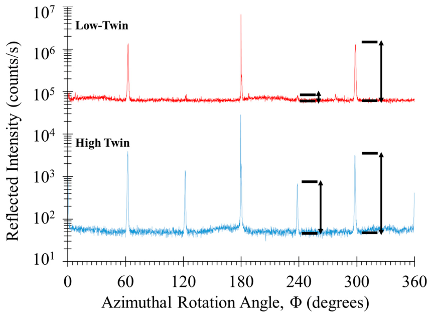
3 via MBE is conclusively demonstrated by the convergence of our structural and optical metrics. The X-ray pole scans (
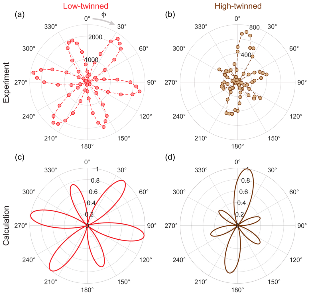
Figure 4) reveal a twin ratio of 100:1, representing a strong preferential domain. This is corroborated by SHG measurements, which show a well-defined six-fold symmetry and stronger intensity (
Figure 5a) in the low-twin sample. This is indicative of an epitaxial material with vanishingly small twin domain structure and reduced antiphase disorder comparable with essentially single-domain, bulk single-crystal Bi
2Se
3 h
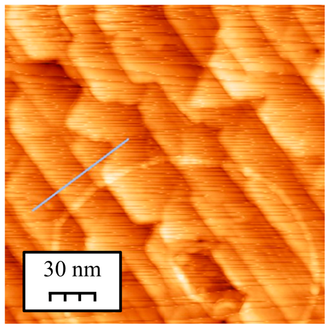
Both the vicinal and the non-vicinal InP substrates have a nominal offcut. The vicinal substrates have a 2° offcut that results in narrower terraces and more step edges to seed preferential domains, resulting in a low twinning density. For the non-vicinal, the offcut is within ±0.5° of the zone axis, resulting in steps that have much wider terraces, and fewer step edges to seed preferential domains, allowing more random domains to form. These step edges can act as a partial polarizer of the emitted SHG field.
Single-crystal Bi
2Se
3 is expected to produce a perfectly six-fold symmetric SHG plot. In
Figure 5a, we observe a slight deviation from that behavior seen as a directional bias, where four lobes are larger than the other two. This most likely originates from the step edges that partially polarize the SHG field. In this case, we need to apply partial polarization to our SHG output by applying the operator
, where
represents the constants,
is the identity operator and
is the polarization tensor at angle
with offset
:
We assume the step edges observed in
Figure 1 define the permitted polarization angle and set
to align the steps with the edges of the Bi
2Se
3 triangular domains. Then we plot
in
Figure 5c and find strong agreement between experiment and theory for the low twinned sample.
The azimuthal dependence of the SHG in the high-twinned samples in
Figure 5b presents a significantly more pronounced two-fold behavior. To account for this variation, we must take into consideration the opposite twinning domain in the material. The SHG tensor for this contribution,
, is computed by subjecting the original
to a
rotation using Equation (2). We can then add the two SHG tensors in unequal contributions to obtain a total SHG tensor [
10]:
where the second twinning domain has a proportion
to the first. We can now compute
which we plot in
Figure 5d, emulating the observed SHG dependence seen in
Figure 5b for the high-twinned sample. In the high-twinned case, we are unsure along which crystal axis the step edges fall; however, for an arbitrary choice of
in
, we find that there will be two large, biased lobes mimicking the data.
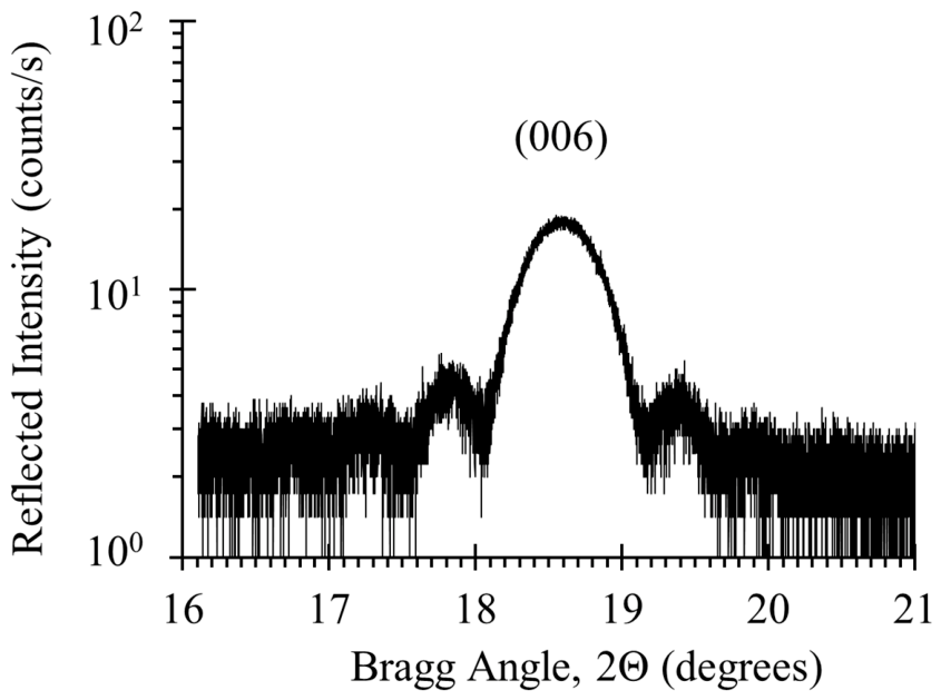
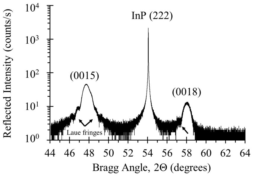
While not studied here, localized planar stacking fault-type defects may also exist pointing out-of-plane within individual domains. This disorder is also equivalent to twinning and probably has a very small impact on the X-ray pole-scan measurement, but more simply acts to induce broadening of the major Bragg peaks observed in symmetric 2-theta scans similar to
Figure 2 and
Figure 3. Because broadening is caused by many factors including thickness and other defects, understanding the effect of only one factor causing broadening would seem intractable.
Such stacking-fault twin disorder has been predicted to have small, but impactful perturbations on the dispersion of the topological surface state [
29]. Separate magnetotransport measurements show that carrier mobility in this family of materials decreases with increasing temperature that is characteristic of phonon dominated, or lattice scattering, and unlikely to impact electrical behavior [
30].
The novelty and significance of this work is that enhanced photonic response from MBE thin-film Bi2Se3 can be obtained by the improved new epitaxial approach described here. In this simple approach, neither substrate roughness nor complicated hetero-structure buffer layers are employed or needed to yield repeatable Bi2Se3 thin-film heterostructures whose photonic quality and performance converge to those of idealized perfect bulk-single crystal material.
5. Conclusions
The nonlinear optical response of thin film topological insulator materials can be adjusted to achieve the idealized bulk response by reducing both antiphase disorder and twin domains. We demonstrate the efficacy of the new approach described here by obtaining a vanishingly small peak-height ratio from X-ray pole-scans showing negligible twinning, new aligned step-flow, terraced growth using atomic force microscopy, and strong SHG signals at the inversion-breaking surface. We corroborate this result with group theoretic analysis of nonlinear optical responses, which shows a dominant six-fold symmetry response in low-twinned samples. The effect of crystalline symmetries is diminished in the high twinned samples, with reduced SHG intensity and a strong preferential SHG axis attributed to the vicinal step structures caused by the miscut of the substrate. The results of this work show that this approach can yield near-perfect single-crystal heteroepitaxial Bi2Se3 whose nonlinear optical responses reflect those of bulk single crystals.
Understanding the impact of these NLO responses on material properties that correlate with photonic behaviors and further refining material quality is a crucial step for realizing chip-scale integrated sensors with strong nonlinear and polarization-dependent responses. A complete picture can be obtained through correlations with, for example, direct photocurrent measurements via time-domain THz spectroscopy on bare samples [
9,
10] or fabricated devices under polarization-dependent illumination.




 ,
,