2. Materials and Methods
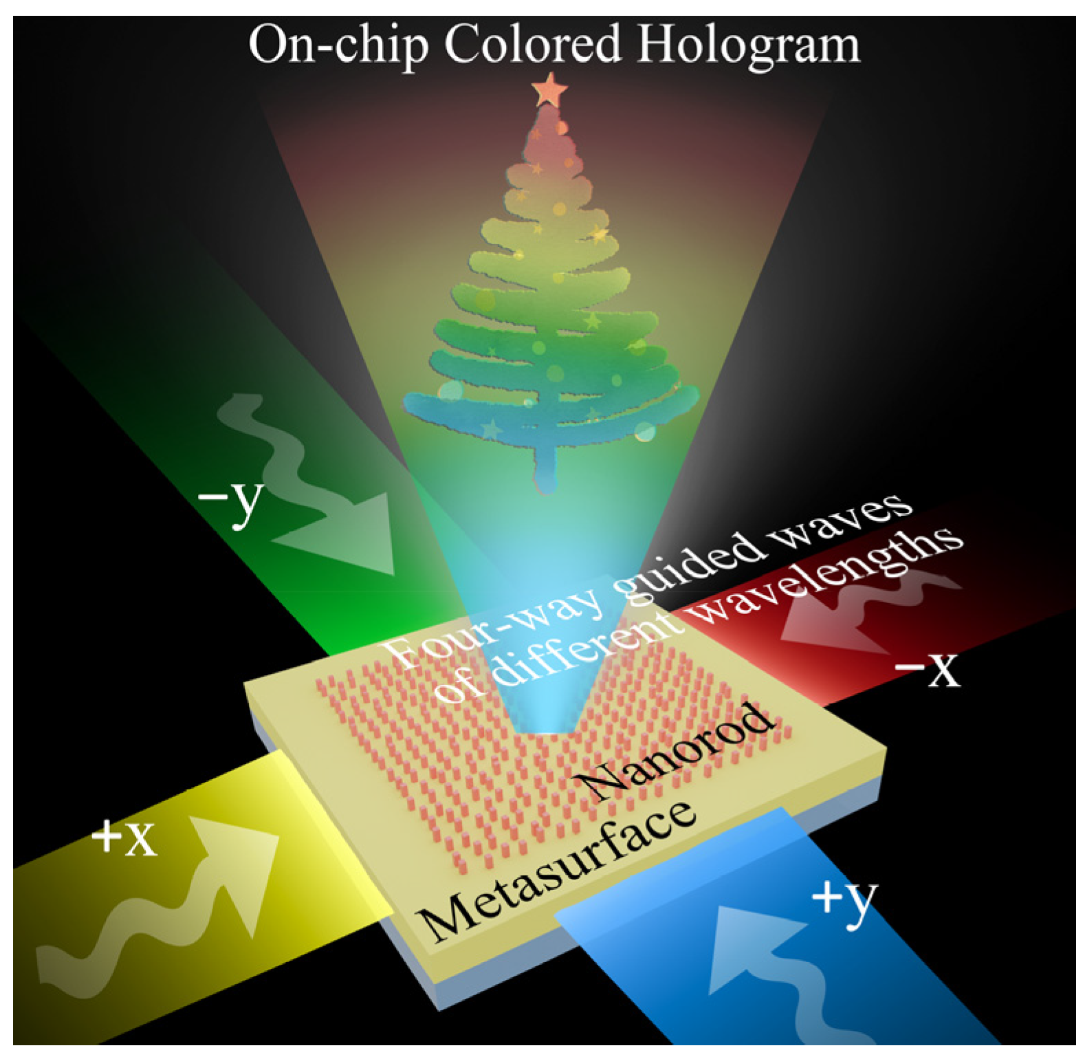
We proposed an on-chip metasurface capable of simultaneously realizing multi-wavelength multiplexed holography. When TE modes of different wavelengths are laterally injected into the waveguide from multiple directions, the specially arranged nanoantennas simultaneously modulate the near-field phase of each wavelength. This enables the target patterns to appear simultaneously in the far field at the desired height, as illustrated in
Figure 1. The physical architecture of the proposed on-chip metasurface utilizes a high-refractive-index contrast dielectric stack rigorously optimized for the visible spectrum. The system is structurally configured into three fundamental layers: a SiO
2 substrate for physical support, a Si
3N
4 core layer for optical transmission, and a top-layer crystalline Si nanoantenna array responsible for optical scattering and phase modulation.
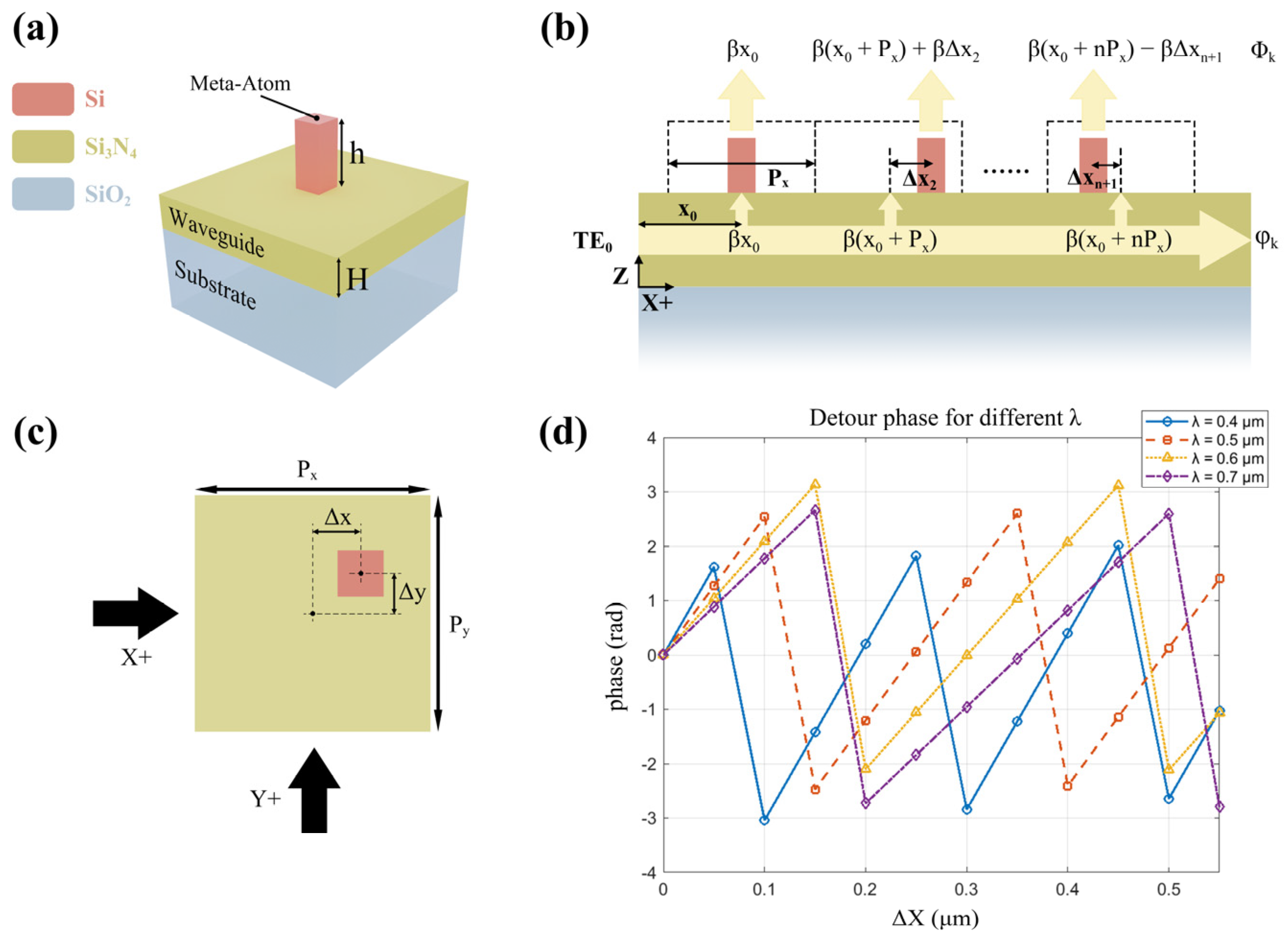
As illustrated in
Figure 2a, the substrate is positioned at the very base of the metasurface device, ensuring sufficient mechanical stability and optical isolation capability. The upper layer comprises a Si
3N
4 waveguide with thickness
H = 1 μm. Such a waveguide thickness can effectively suppress the influence of evanescent fields near the waveguide surface on the scattering behavior of the meta-atoms, while remaining within a practically achievable fabrication range [
13]. Given Si
3N
4’s high refractive index in the visible spectrum (
n ≈ 2.05) and its near-zero imaginary part in this wavelength range, this waveguide layer not only effectively confines the TE mode within the waveguide, thereby mitigating the impact of evanescent waves [
14] on holographic outcomes, but also enables near-lossless forward propagation of the TE mode within the waveguide.
This effectively reduces the constraints on metasurface design scale within compact spaces. A nanoantenna array is positioned atop the waveguide, with each nanoantenna comprising a rectangular prism of length l = 160 nm, width w = 160 nm, and height h = 380 nm, arranged periodically in the x/y directions with a period Px = Py = 550 nm. The entire nanoantenna array region comprises 101 × 101 periodic cells, each containing a positionally tunable antenna unit cell.
In this design, we regulate the metasurface phase based on the detour phase, which is regarded here as the phase accumulation resulting from the propagation of the guided wave within the waveguide [
15]. As illustrated in
Figure 2b, when the TE
0 mode is injected from the waveguide sidewall, the light wave of this mode is confined within the silicon nitride layer and propagates forward along the injection direction. Owing to negligible mode leakage, the propagation may be approximated as occurring within a homogeneous medium of effective refractive index
neff. As propagation distance increases, the light wave continuously accumulates phase; this phase accumulation during mode propagation within the waveguide constitutes the propagation phase. The accumulated propagation phase at various points within the waveguide may be expressed as:
where
β denotes the phase propagation constant, and
x represents the distance along the injection direction from the mode injection point to a point on the metasurface. For any given wavelength
λ, the propagation constant may be defined as:
From Equation (2), it can be seen that when guided waves of different wavelengths propagate within the same waveguide, both the wavelength λ and the effective refractive index neff vary accordingly, resulting in a strong wavelength dependence of the propagation constant β.
When the guided wave propagates along the defined forward direction within the waveguide from the center of the first periodic cell to the center of the (
n + 1)th periodic cell, its propagation distance can be expressed as
nP, where
P denotes the cell width in the propagation direction (
Px along the
x-axis and
Py along the
y-axis). Consequently, the phase of the guided wave at this position is
. Evidently, relying solely on the accumulated propagation phase of the guided wave at various points proves insufficient for achieving precise phase control across the metasurface. To realize customizable phase discontinuities within each periodic unit, we introduce the relative displacement value Δ
xk for each nanoantenna within a cell. This value represents the offset of the nanoantenna relative to the cell center along the propagation direction. When the guided wave reaches the (
n + 1)th cell, the displacement of the antenna from the cell center alters the position where the guided wave is coupled into free space, introducing an additional phase jump,
βΔ
xn+1. At this point, the total phase jump within this cell can be expressed as:
The detour phase distribution within each periodic unit cell of the metasurface can be characterized by the above equation. Consequently, precise control over the relative displacement Δ
x of the nanoantennas within each unit cell enables comprehensive regulation of the detour phase distribution. Extensive calculations demonstrate that when the propagation period
P = 0.55 μm, complete phase coverage from
can be achieved within the visible light spectrum. Compared to resonant phase, propagation phase, and geometric phase, the detour phase is independent of shape, material, rotation angle, and polarization. It controls phase by adjusting the placement of nanoantennas within the unit cell—that is, by altering the propagation path length of light within the waveguide. Consequently, it exhibits superior polarization compatibility and structural scalability [
16]. This enables complex spatial phase encoding within a single structure, demonstrating broad application prospects and providing a simple yet efficient solution for realizing multi-wavelength holography.
To achieve the reconstruction of a specific light field in free space, the first step is to determine the phase distribution corresponding to each periodic unit cell of the metasurface, namely the phase map. Computer-generated holography provides an effective means of algorithmically inverting this phase distribution. Typically, it takes the target light field as input, undergoes a series of inversion algorithms and iterative processes, ultimately outputting the wavefront phase distribution required to generate the desired light field. In this study, we employed the Gerchberg-Saxton (GS) algorithm [
17]—the most classical and widely applied phase inversion method—to determine near-field phase-maps for different wavelengths. In essence, the algorithm combines the given near-field amplitude distribution
with a randomly initialized phase distribution
to form the initial light field. This is then Fourier transformed to compute the light field distribution propagating to the target far-field. At the far-field plane, the amplitude information is replaced with the amplitude distribution
of the target image while retaining its phase distribution, thereby introducing constraints from the target light field. Subsequently, the inverse Fourier transform returns to the near field, where constraints are reimposed using the near-field amplitude
. This sequence constitutes a complete iteration, with the resulting light field serving as the initial input for the next iteration. As iterations progress, the far-field light field gradually converges towards the target image. Iteration ceases when the error calculated by the evaluation function falls below a preset threshold or the predetermined iteration count is reached. At this point, the derived near-field phase distribution
constitutes the holographic phase map capable of reconstructing the desired light field at the target plane [
18]. Based on this process, we computed the initial phases
,
,
,
for the near-field at different wavelengths. By employing detour phase modulation to ensure the phase discontinuities of each metasurface unit satisfy the computed phase-map, single-wavelength holographic imaging can be achieved. Concurrently, the phase-maps for each wavelength lay the groundwork for subsequent multi-wavelength multiplexed holography.
In numerous metasurface multi-wavelength multiplexing designs, to satisfy phase requirements across different wavelengths within the same structure, researchers typically employ the following formula [
19]:
Among these, denotes the required phase-map across different frequency bands. By superimposing the phase distributions required at various wavelengths into a single composite phase distribution via Equation (4), a metasurface capable of simultaneously satisfying this integrated phase distribution across all wavelengths can achieve multi-wavelength multiplexing within a single device. Research employing Pancharatnam–Berry (PB) phase modulation demonstrates its suitability for this composite phase distribution. Since PB phase satisfies the relationship between the rotation angle of the nanoantenna and twice the phase jump at any wavelength, its phase jump remains independent of the operating wavelength. Consequently, PB phase can effectively fulfill this composite phase distribution: Simply selecting an appropriate rotation angle for each unit cell to provide the same geometric phase as the combined phase enables simultaneous phase satisfaction across multiple wavelengths. By contrast, the detour phase exhibits strong wavelength dependence: its realization relies on the phase propagation constant β. As previously noted, β’s value is highly correlated with the guided wave wavelength, leading to phase jumps induced by nanomaterial antenna displacements Δx varying with wavelength. In other words, applying identical displacement to nanoantennas within the same unit of a metasurface cannot yield consistent phase jumps across all wavelengths. Consequently, when phase control relies solely on the relative displacement-induced detour phase, directly applying Equation (4) to achieve a single phase satisfying multiple wavelengths proves unfeasible. Viewed alternatively, applying identical displacement to nanoantennas within the same unit of a metasurface produces distinct phase jumps across different frequency bands. This significantly reduces the probability that the same relative displacement will generate holograms displaying only the primary image and its conjugate image, thereby demonstrating the potential for multi-wavelength multiplexed holography through detour phase modulation.
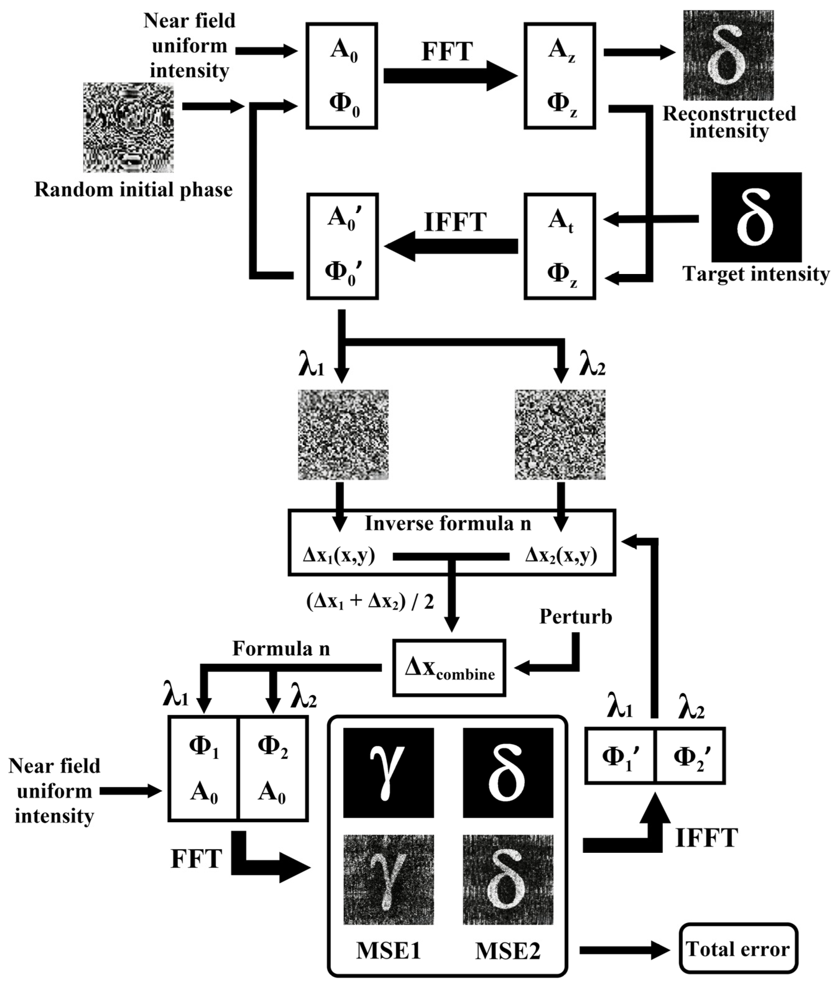
To address the challenge of simultaneously regulating detour phase across multiple wavelengths under multi-wavelength conditions, this study proposes a ‘phase-displacement-joint displacement’ multi-wavelength multiplexing algorithm. This algorithm transforms the phase distributions across wavelengths into relative displacement distributions under detour phase control. By jointly optimizing the displacement distributions at different wavelengths, a single metasurface can successfully reconstruct the desired holographic patterns across all bands under unified detour phase control. As illustrated in
Figure 3: First, we compute the required near-field phase distributions for wavelengths
λ1 and
λ2 using the aforementioned GS algorithm inversion. Subsequently, these phase-maps are converted into the required relative displacement distributions Δ
x1(
x,
y) and Δ
x2(
x,
y) for the nanoantennas via Equation (3). At this stage, we averaged these two relative displacements to construct the combined displacement distribution
, which can be interpreted as an equal-weight combination of contributions from different channels, serving as the initial input for the multiplexing algorithm. Upon entering the multiplexing algorithm, Δ
xcombine was reverse-calculated to yield its corresponding phase-maps at
λ1 and
λ2, representing the phase components
and
of the near-field. These were then combined with the standard near-field intensity
A0 to form the initial near-field distributions
and
. Similar to the GS algorithm workflow mentioned earlier, a simultaneous bidirectional Fourier transform is applied to
U1 and
U2. The phase information carried by the resulting
and
undergoes displacement. Consequently, the displacement distributions derived inversely from
and
become unequal, preventing Δ
xcombine from remaining joint. In other words,
and
now more closely approximate the phase distributions required for single wavelengths
λ1 and
λ2, respectively. Consequently, the converted
and
become more aligned with the relative displacement distributions needed for single wavelengths, causing the multi-wavelength multiplexed hologram to shift towards a single-wavelength hologram. This shift is not necessarily detrimental. It allows the combined displacement to achieve far-field effects across wavelengths that more closely resemble those of a single wavelength. Simultaneously, it introduces perturbation into each iteration’s outcome, preventing overfitting during the iterative process. Finally, the average of
and
is taken as Δ
xcombine for the next iteration.
To achieve global coordination and error suppression across multiple wavelengths, this paper introduces the simulated annealing algorithm as the core optimization strategy. Simulated annealing originates from the thermodynamic process of solid annealing, employing a probabilistic mechanism to accept solutions with slightly higher error to prevent the optimization from becoming trapped in local minima. This algorithm exhibits robust global search capabilities in its early stages, gradually stabilizing towards convergence as the temperature decreases. It effectively locates solutions Δxcombine approximating the global optimum within complex, multidimensional solution spaces. The annealing temperature follows an exponential decay law , where T0 = 0.1, = 8000, and i denotes the iteration round number. This parameter combination, validated through multiple simulations, achieves a favorable balance between convergence speed and result stability. In principle, further optimization of the annealing parameters may provide additional reductions in the MSE and further improve the reconstruction quality. Upon incorporating the simulated annealing algorithm, the total mean squared error (MSE1 + MSE2) between the far-field intensity values at each wavelength during iteration and the target image is calculated. This determines the effectiveness of the current Δxcombine iteration in realizing holographic effects across all wavelengths, thereby deciding whether to retain the Δxcombine value. This process guides the iteration towards convergence that simultaneously satisfies multi-wavelength multiplexing holography.
3. Results
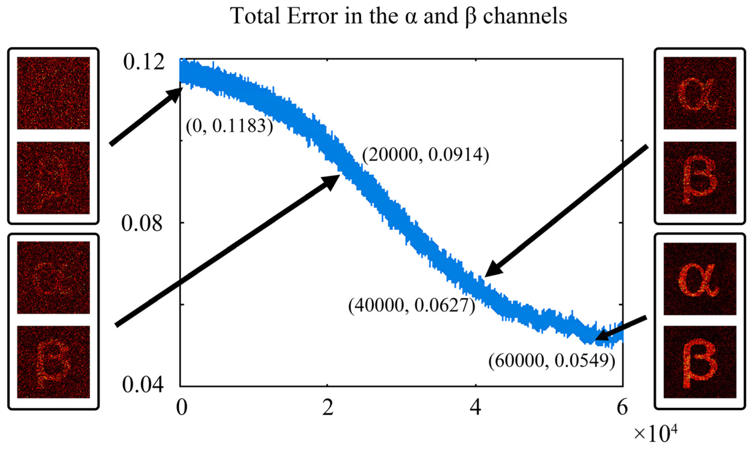
Setting the algorithm iteration count to 60,000 cycles, the intensity difference between the target pattern and the currently computed far-field holographic pattern is calculated as the Total Error at the conclusion of each iteration. This yields the curve depicted in
Figure 4. It demonstrates that the Total Error undergoes a phased decay process with increasing iteration count: initially gradual, then accelerating, before slowing again. During the initial iteration phase, the simulated annealing algorithm operates at a high ‘temperature’ search stage, applying substantial perturbations to the solution. The algorithm favors exploring diverse combinations of joint displacement distributions across a broader range to avoid premature convergence to local optima. Consequently, while the solution undergoes continuous adjustment, it has yet to stabilize towards an effective convergence direction, resulting in a relatively gradual error reduction rate. As the iteration count increased, the temperature parameter gradually decreased. The search transitioned from global exploration to a directed optimization phase centered around the current favorable solution. The joint displacement distribution began to refine and correct around the optimal solution, rapidly improving the match between the far-field light field and the target distribution. This propelled the error into a phase of rapid decline. During late-stage iterations, the system approaches the vicinity of the optimal or suboptimal solution. The probability of accepting suboptimal solutions diminishes significantly, causing the error reduction to slow again and gradually stabilize. Ultimately, convergence occurs near a local optimum, with the error fluctuating minimally around this point. Every 20,000 iterations, we read the far-field light field computed from the joint displacement of that iteration. Taking the far-field hologram of channels
α and
β as an example, as the iteration count increases, the pattern contours become increasingly distinct. Light field energy concentrates more intensely within the target pattern region, background noise is significantly suppressed, and pattern contrast markedly improves. This demonstrates that the multiplexing algorithm effectively guides the joint displacement distribution toward solutions that simultaneously satisfy constraints across multiple wavelengths. Although the current optimization framework exhibits effective performance at the demonstrated scale, computational cost and runtime may become increasingly challenging when extending the optimization to arrays containing millions of elements. The test results indicate that, although 60,000 iterations were used in this study, a reduced number of iterations (e.g., 20,000) may still achieve comparable performance in practice, thereby improving the practicality of the proposed framework for large-scale design problems.
Through the aforementioned algorithm, we obtained two sets of fusion displacement distributions Δxcombine and Δycombine corresponding to the x-direction and y-direction respectively. Here, Δxcombine is calculated from the input λγ, λδ and their corresponding phase distributions , ; Δycombine is calculated from the input λα, λβ and their corresponding phase distributions , . Inputting Δxcombine and Δycombine into Lumerical FDTD, for the aforementioned metasurface with periodically placed nanoantennas, Δxcombine controls the arrangement position of the nanoantennas along the x-axis, while Δycombine controls their arrangement position along the y-axis. Under the simultaneous control of these two combined displacement distributions, each displacement parameter governs the detour phase for two wavelengths of holographic imaging. This configuration enables the metasurface to support four-wavelength, four-channel holographic imaging concurrently.
To validate the performance of four-wavelength, four-channel holographic imaging, we employed Ansys Lumerical 2023 R1 FDTD software for visualization. First, we precisely arranged the global nanoantennas on the Si
3N
4 waveguide according to the combined displacement in the
x and
y directions. TE
0 mode light sources with wavelengths
λγ = 0.6 μm,
λδ = 0.7 μm,
λα = 0.4 μm,
λβ = 0.5 μm were set along the +
x, −
x, +
y, −
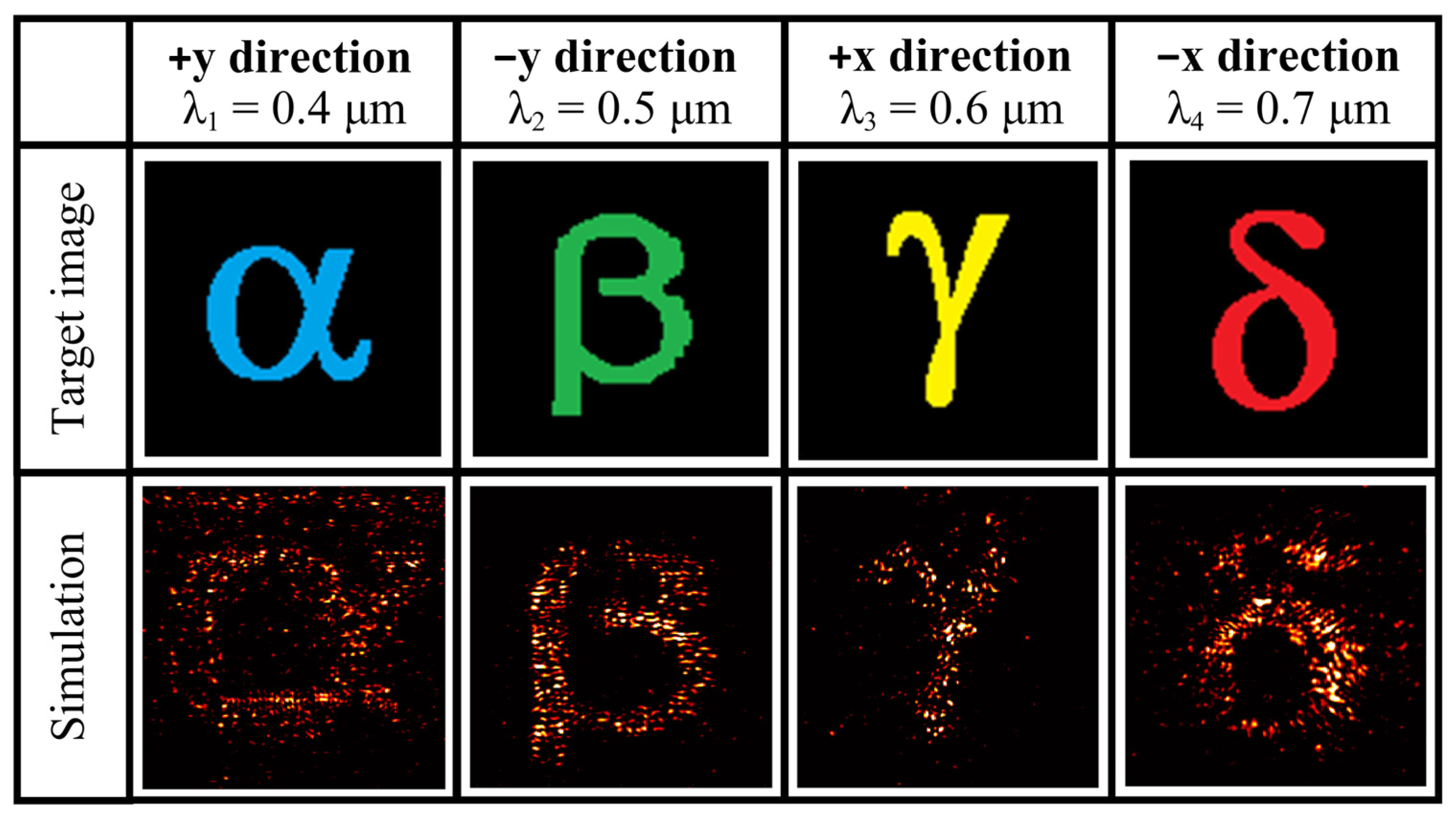
y directions respectively, enabling lateral injection of light into the waveguide. Simultaneously, monitors corresponding to each wavelength were positioned at the anticipated holographic plane located 50 μm above the metasurface. The simulation results are shown in
Figure 5. Under simultaneous injection of TE
0 modes across four distinct wavelength bands, distinct holographic patterns for each band were observed in the monitors of respective channels within the target region. It can be seen that the simulated holographic patterns align precisely with the target patterns in terms of position, shape contour, and imaging direction. Furthermore, minimal crosstalk was observed between patterns of different bands, demonstrating highly independent holographic performance.
To quantitatively evaluate the imaging quality, the reconstructed holograms were characterized using the mean squared error (MSE), peak signal-to-noise ratio (PSNR), and structural similarity index measure (SSIM). The α channel achieved an MSE of 0.0106, a PSNR of 19.7307 dB, and an SSIM of 0.1802. The β channel exhibited an MSE of 0.0039, a PSNR of 24.1170 dB, and an SSIM of 0.3910. For the γ channel, the corresponding values were 0.0031, 25.1843 dB, and 0.3917, respectively. Meanwhile, the δ channel obtained an MSE of 0.0052, a PSNR of 22.8552 dB, and an SSIM of 0.3550. These results indicate that the β and γ channels exhibit relatively improved reconstruction fidelity, while the α channel operating at shorter wavelengths shows comparatively reduced performance. This behavior is mainly attributed to the stronger dispersive absorption of silicon in the short-wavelength visible band. In particular, the extinction coefficient of silicon increases significantly at 0.4 μm, resulting in higher optical absorption loss compared with the longer wavelength channels [
20].
4. Discussion
The detour phase exhibits wavelength dependence due to the phase propagation constant β, causing identical relative displacements across different bands to produce varying phase discontinuities. Whilst this characteristic increases the complexity of multi-wavelength control, it also mitigates the degree of mutual interference between patterns in different bands. Consequently, holographic imaging at distinct wavelengths exhibits a high level of mutual independence, thereby reducing the probability of crosstalk between images.
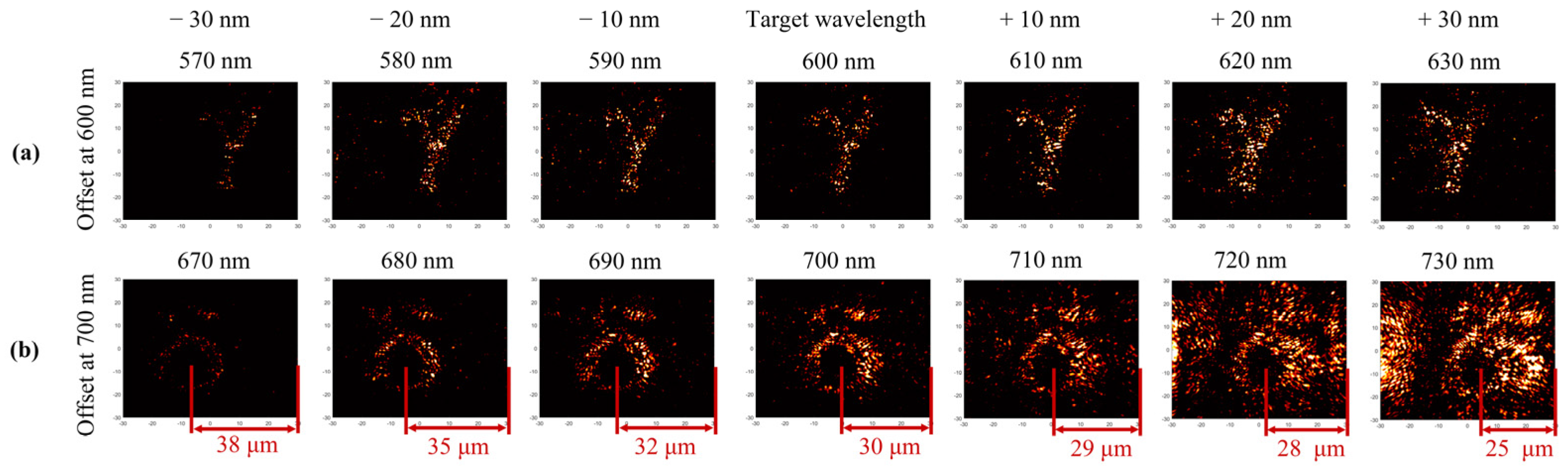
To systematically evaluate spectral robustness, the research team conducted dense wavelength sweep simulations in FDTD over a continuous broadband range of ±30 nm relative to the central wavelengths. Systematic data analysis reveals a difference in spectral tolerance between the short-wavelength and long-wavelength channels of the proposed system. The displacement of the far-field holographic image and the wavelength deviation are shown in
Figure 6. The γ group exhibits a broad operational bandwidth, maintaining its designed shape even at deviations of ±30 nm with only slight displacement. The δ group demonstrates significant image distortion or markedly degraded imaging quality when deviations exceed 10 nm. These metasurface holographic simulation results across the bands demonstrate that altering the operating wavelength relative to the design wavelength significantly impacts the simulated holographic image. This causes shifts in both the intensity and spatial position of the imaging, introduces noise, and results in imaging effects deviating from the intended target image. Furthermore, as the operating wavelength progressively increases from left to right, the nanoantennas couple a greater portion of optical energy at this wavelength. Consequently, the TE mode emits more energy into the far field, resulting in a brighter holographic pattern as measured by the monitor.
We also compared the current-scale metasurface with multiple sets of smaller-scale metasurfaces and larger-scale metasurfaces. Quantitative evaluation metrics for different scales of metasurface arrays are shown in
Table 1. Smaller-scale metasurfaces, constrained by the number of units and spatial sampling density, still exhibit certain shortcomings in the reconstructed light field regarding detail, continuity, and intensity uniformity, often manifesting as edge blurring or fragmented imaging. In contrast, as the metasurface array scale increases, both light field continuity and imaging accuracy show marked improvement, with a clear trend towards enhanced holographic imaging quality.
Compared with other holographic imaging approaches in
Table 2, our method employs a single detour phase modulation technique to achieve customizable holographic multiplexed imaging within the 0.4~0.7 μm wavelength band across a compact area of 55.55 × 55.55 μm
2. This demonstrates significant advantages in both device area and multiplexing capability.
Moreover, in numerous designs, phase distribution across individual cells is achieved by modulating variations in the nanoantenna structure [
24,
25], such as PB phase, geometric phase, resonant phase, and so forth. These phase-modulation approaches prove difficult to adapt for applications in which the nanoantenna geometry is constrained by additional functional requirements. In contrast, the phase-modulation method employed herein relies solely on detour phase involving relative displacement, exhibiting minimal dependence on the nanoantenna’s structural configuration. This affords considerable design flexibility for the nanostructure geometry, enabling substantial exploitation of structural modifications to achieve other compelling effects. For instance, manipulating the nanostructure can enhance extraction efficiency for different wavelengths. Concurrently, the multi-wavelength multiplexing approach described herein enables comprehensive control over both wavelength and phase within the on-chip metasurface, facilitating high-precision, multi-multiplexed color holographic displays in free space.
The proposed scheme is compatible with existing nanofabrication technologies and is therefore experimentally feasible. Recent advances in nanofabrication techniques, such as electron-beam lithography (EBL) and reactive ion etching (RIE), have demonstrated positioning accuracies on the order of several nanometers, which are sufficient for implementing the proposed design [
13,
15]. In addition, small deviations in the height and lateral dimensions of the meta-atoms within a reasonable range are expected to have a limited impact on the overall imaging performance, indicating that the proposed approach exhibits a certain degree of fabrication tolerance.
In this study, different holographic channels are distinguished by combinations of wavelength and injection direction, enabling the encoding of corresponding far-field holographic patterns. However, due to the intrinsic wavelength dependence of the detour phase, increasing the number of multiplexed wavelengths makes it increasingly difficult for the multi-wavelength multiplexing algorithm to simultaneously satisfy the required phase discontinuities of all channels. As a result, accurate phase matching becomes progressively more challenging, which may lead to degradation in the quality of the reconstructed far-field holographic images. This indicates that, within the current modulation framework, expanding the number of channels solely along the wavelength dimension has inherent limitations. As a potential extension, the spatial mapping property of the Maxwell’s fisheye lens can be considered [
26]. Such systems establish a one-to-one correspondence between different spatial positions, enabling physical separation of distinct signal channels. By introducing this spatial mapping mechanism into on-chip metasurface design, it is possible to incorporate an additional spatial degree of freedom beyond wavelength and incident direction. This allows channel information to be distributed into different spatial regions during propagation or imaging, thereby reducing inter-wavelength coupling and offering a feasible pathway toward enhanced channel capacity and system scalability.
By decoupling the physical requirements of phase modulation from the local geometric shape of the nanoantenna itself, this architecture immensely liberates the design degrees of freedom for internal nanostructure parameters. This profound design decoupling implies that in future iterations, the specific height, width, and cross-sectional shape of the crystalline silicon pillars can serve as independent variables fed into topology optimization algorithms, specifically engineered to maximize optical extraction efficiency or dictate beam directionality for different wavelength channels—all without disrupting or degrading the holographic phase profile already encoded in their spatial arrangement.



 ,
,