1. Introduction
In programmable photonic integrated circuits (PPICs), light routing is implemented by interconnecting photonic building blocks with waveguides, forming a configurable mesh of optical paths. Reconfigurable meshes typically use 2 × 2 units as the basic switching element, commonly implemented with tunable directional couplers (TDCs) [
1], multimode interferometers (MMIs) [
2,
3], or Mach–Zehnder interferometers (MZIs) [
4,
5]. Each 2 × 2 unit can implement bar/cross switching and power splitting (partial), and by cascading these units it is possible to obtain reconfigurable networks for routing, combining, and real-time matrix–vector multiplication (MVM).
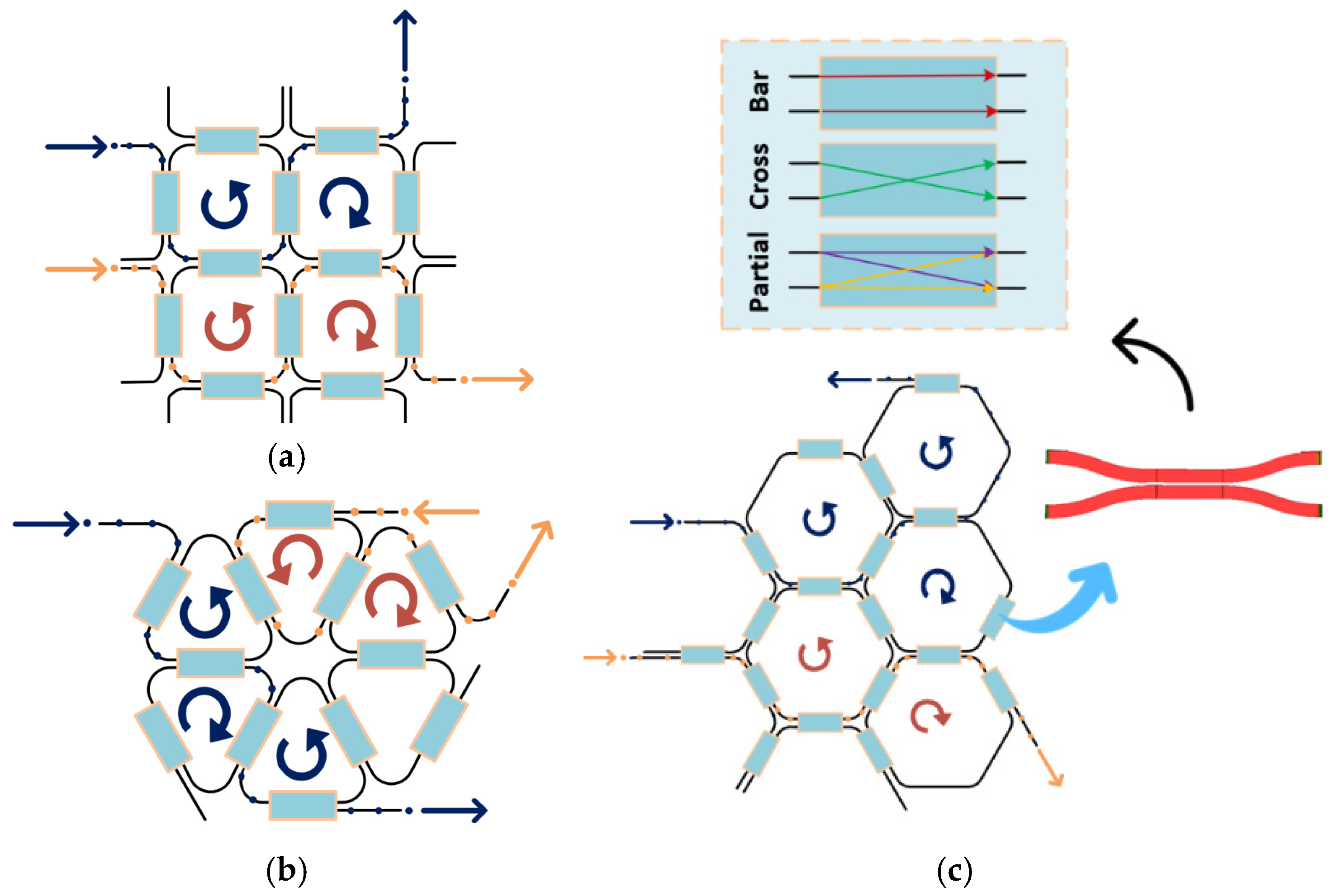
In 2015, Zhuang proposed a square mesh topology, adding feedback (loops) within the circuit [
6], as illustrated in
Figure 1a. Then, in 2016, Capmany extended the concept to triangular/hexagonal topologies [
7], shown in
Figure 1b,c, enabling denser and more complex optical networks.
Directional couplers based on two parallel waveguides can be designed as splitters, combiners, or power distributors, depending on geometry (width, coupling length, and gap). As passive devices, their response is fixed after fabrication and cannot be reprogrammed. To enable dynamic control, optoelectronic actuators are integrated to modify the optical properties of the active region, turning the coupler into a tunable element. Common approaches include the thermo-optic effect (TOE) [
9,
10,
11], electro-optic effect (EOE) [
12,
13,
14], and free-carrier plasma dispersion effect (FCPDE) [
15,
16,
17]. These mechanisms are widely used for modulation, switching, and synchronization, and form the basis of many programmable photonic platforms.
Among these techniques, the TOE is attractive due to its simple implementation and compatibility with multiple PIC platforms (SiO2-Si
3N
4, SOI, InP) and standard CMOS processes [
8]. Because it does not rely on carrier injection or resonant effects, it can provide low additional optical loss and robust operation. In practice, the TOE is implemented as thermo-optic phase shifters (TOPSs) using metal heaters, transparent conductive oxides (TCOs), doped silicon/silicides, or 2D materials (e.g., graphene and carbon nanotubes) [
10]. Heaters are placed near the waveguide to increase thermal efficiency but placing them too close can introduce optical loss (metal absorption or carrier absorption), mode disturbance, stress/birefringence, and reliability issues. Therefore, an insulating spacer is usually introduced between the heater and waveguide. For metal heaters, common insulating layers include SiO
2, Si
3N
4, and Al
2O
3, with typical vertical gaps of 1.0–2.0 µm to achieve good thermal efficiency with low insertion loss (IL) [
10]. Alternative solutions include adding a thin AlN layer to channel heat toward the waveguide without moving the metal closer [
18]. For transparent heaters (e.g., ITO, graphene), the spacer can be reduced (≈0.1–0.5 µm) while keeping negligible optical loss, and in doped heaters the highly doped region is commonly kept ≥0.5–1.0 µm from the mode maximum to limit absorption. In general, efficiency and response result from a compromise between thermal gradient, optical loss, and thermal isolation from the substrate [
9].
A main limitation of TOPSs is modulation speed (kHz–MHz) [
19], typically constrained by thermal diffusion and the thermal time constant. After a power step, the switching dynamics can be characterized by a thermal response time constant
, while the tuning efficiency is often discussed in terms of the electrical power
required to induce a
phase shift [
20]. Both quantities are influenced by heat spreading, thermal drift, and thermal crosstalk in dense layouts.
Recent approaches aim to reduce
, insertion loss (IL), and crosstalk without significantly increasing cost. Examples include: (i) thermal isolation via substrate undercut and trenches/air, which concentrate heat in the guide and reduce lateral leakage; (ii) folded/multi-pass layouts that concentrate heating in the target region and improve heater utilization (η) [
9]; (iii) deep trenches between neighboring cells to provide thermal isolation with limited impact on compactness; (iv) transparent heaters near the guide (TCO/2D) shortening the thermal path: less gradient and shorter diffusion time, reducing power and local crosstalk without adding metal losses [
10]; (v) thermal channeling with a thin AlN (high conductivity compared to SiO
2) sheet that conducts heat toward the guide while preserving optical isolation [
18]; and (vi) active algorithmic mitigation through thermal sensing and adjustments [
21]. All these techniques implement solutions that in many cases penalize design complexity, manufacturing, and integration processes.
Motivated by this trade-off, this work proposes a new structure, the shallow-rib strip directional coupler, that shifts coupling control from the lateral gap to the slab height and uses adiabatic access regions. This enables efficient operation with larger waveguide separations and relaxed lithography and etch tolerances, while also mitigating thermal crosstalk.
The remainder of the paper is organized as follows.
Section 2 reviews directional couplers using coupled-mode theory (CMT) and introduces thermo-optic control.
Section 3 presents the shallow-rib strip configuration and its thermo-optic implementation. Finally, we demonstrate a 4 × 4 switching matrix built from thermo-optic shallow-rib strip 2 × 2 cells as a scalable example toward larger N × N arrays.
2. Directional Coupler
The directional coupler is one of the most fundamental structures in integrated photonics and is widely used in programmable photonic mesh networks [
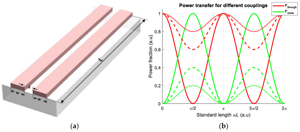
8]. It is employed in passive and active components such as optical power splitters, modulators, wavelength division multiplexers, add–drop multiplexers, and as part of interferometric structures such as Mach–Zehnder interferometers. A straight directional coupler consists of two adjacent parallel waveguides separated by a small gap [
22], as show in
Figure 2. Coupled-mode theory (CMT) describes how electromagnetic modes propagate and interact along the longitudinal
z-axis due to the superposition of fields resulting from the guide’s physical properties and design parameters, such as length, width, height, and angle.
Modern textbook treatments and recent works often adopt simplified coupled-mode formulations that provide an intuitive description compared to the classical derivation [
23,
24,
25,
26], while remaining consistent with the formal framework reported in [
27,
28]. This model expresses the coupling equations for two identical parallel rectangular waveguides, as shown in
Figure 2, with propagation constants
and
and coupling coefficients
and
, considering the losses
ɑ, where the total electric field of a guided mode in a waveguide is determined by
where
is a complex amplitude that includes the propagation phase
;
is the transverse mode profile, normalized to carry unit power. The optical power in each guide is given by
In the general case, the coupling between modes, the amplitudes evolve according to
Assuming identical waveguides with loss
, we set
where
is the coupling coefficient,
is the propagation constant and
is its real part; assuming no phase mismatch (
), we express the coupling equations between modes as follows:
The solution to this system can be modeled as a transfer matrix given by
For conditions
and
, the power flow in the guides is given by
describing a sinusoidal power exchange modulated by exponential attenuation due to propagation loss
α. The length
Lc needed for complete power transfer from one guide to another is given by
where
, in a real guide, with absorption and scattering losses;
is complex. At
=
, assuming that the input optical power is
and that it is initially found in the waveguide
, the power in each waveguide evolves as follows:
where the coupling coefficient is given by
where
is the channel width;
is the separation. In the propagation on the
y-axis,
h and
q are the propagation constant and the extinction coefficient, defined as
and
respectively, for
[
29]; on the
z-axis, we have
β as the propagation constant [
27], obtained from the characteristic equation of the guided mode. For TE polarization, the dispersion relation is given by
where
is the mode order.
In photonic modeling and measurement, it is customary to define the field transmission coefficients at the output of a lossless directional coupler of length as where and are the complex field amplitude coefficients for the through (bar) and cross states, respectively.
The corresponding power transfer coefficients are defined as
with the energy conservation condition (lossless case)
From coupled-mode theory, for identical waveguides and no phase mismatch, the field coefficients are [
27]
which leads to power fractions
where
is the input optical power,
is the power remaining in the original (bar/through) waveguide and
is the power coupled to the adjacent (cross) waveguide. As shown in
Figure 2b, for different separations
between the waveguides, the coupled optical power decreases, as determined by the coupling ratio in Equation (14).
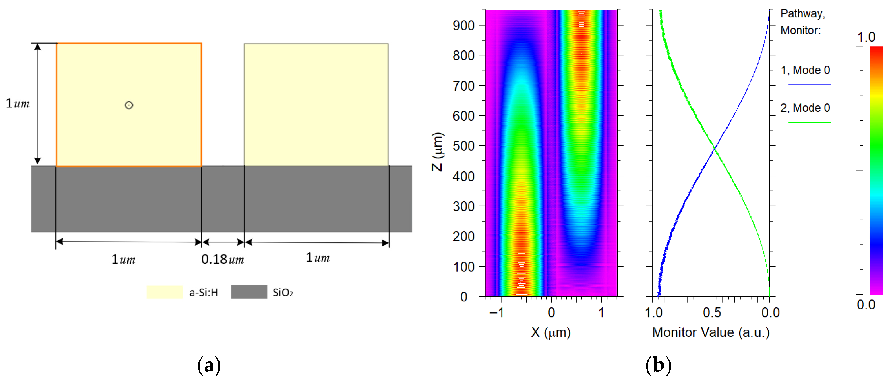
To analyze coupling in the structure of
Figure 2a, we simulated two identical parallel a-Si:H waveguides on a SiO
2 substrate with air as the top cladding. The interaction length was set to
μm and
= 0.18 μm. Simulations (cfr.
Figure 3) were performed in RSoft CAD (2024-09 Keysights) using the BeamPROP (BPM) using the 3D simulation model [
30]. Refractive-index data were taken from the refractiveindex.info database published by Mikhail Polyanskiy [
31], based on the room-temperature measurements reported by Franta for the corresponding materials [
32,
33].
As indicated by Equation (14), the coupling coefficient depends on the inter-waveguide gap , which controls the overlap of the evanescent fields between the guides. When is small, the coupling is greater, resulting in a lower Lc required for complete coupling. If there is also a phase mismatch due to a difference in effective indices, the coupling is further reduced, even for short separations. As increases, the modal overlap falls rapidly, becomes small, and Lc grows, eventually leading to negligible power transfer.
As mentioned, a passive directional coupler fixes its response by geometry (, ) and does not allow dynamic control. To enable reconfiguration without changing the geometry or position of the device, optoelectronic techniques are used to modify the optical properties of the active segment in situ. By varying the effective mode index, the propagation constant changes and, therefore, the modal parameters of the coupler change (, ), allowing the output power (bar/cross/partial) to be controlled.
Thermo-Optic Directional Coupler
Due to its ease of implementation and high compatibility with SOI/CMOS fabrication, the thermo-optic effect is widely used for tuning and control in directional couplers [
10]. In this approach, the effective refractive index of the waveguide segment under the heater is modified by a temperature change according to
where the effective thermo-optic coefficient of the guided mode is defined as
, also known as the thermal coefficient, and Δ
T is the heater-induced temperature variation. This variation in the refractive index introduces a variation in the propagation constant
as [
10]
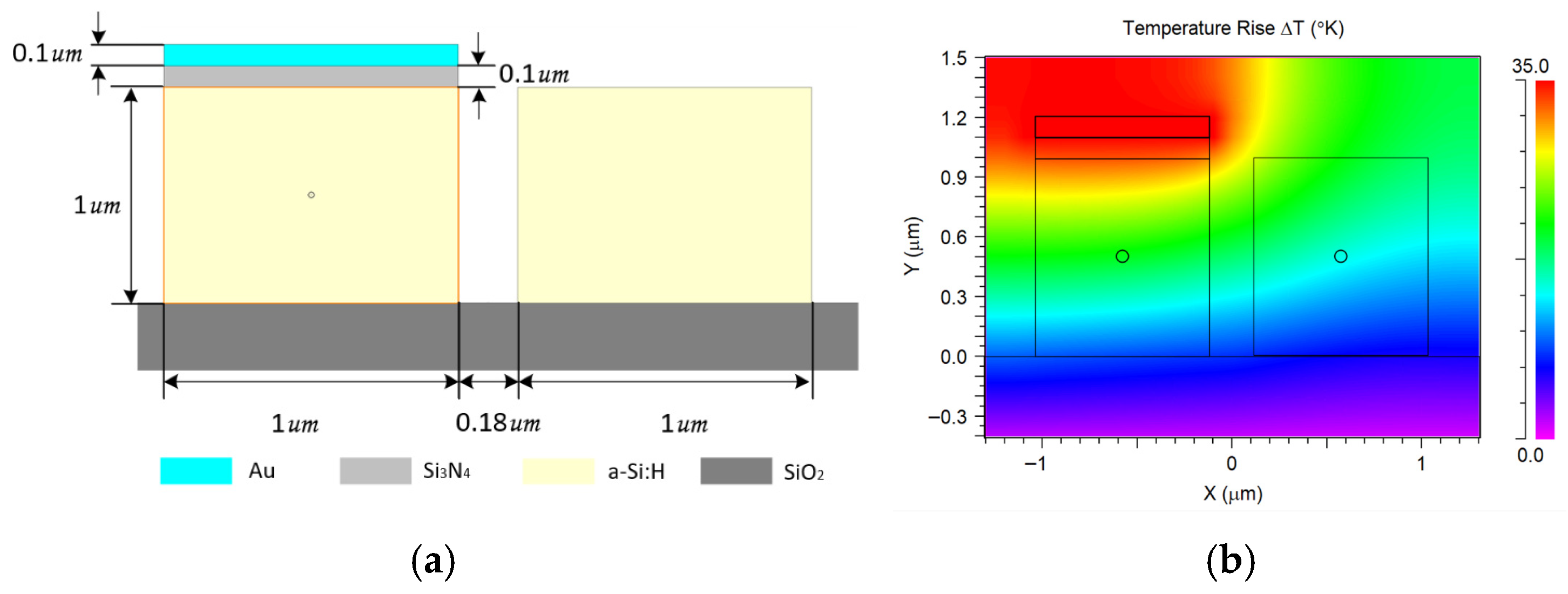
In thermo-optic directional couplers, thermal crosstalk may occur because the heater’s thermal conduction region can partially heat the adjacent waveguide, as shown in
Figure 4b. This effect induces unwanted heating in the adjacent guide, creating a lateral thermal gradient that changes
and
unevenly (
≠ 0) and detunes the coupling, even if
remains unchanged. When changes are introduced in the unwanted guide (
), the modal balance is degraded, leading to unwanted changes in the phase/coupling state of the adjacent arm, which shift the operating point and introduce slow drift (ms).
To analyze the configuration in
Figure 4, we used the same structure and parameters as in
Figure 3 (two identical a-Si:H guides on SiO
2 with
= 950 μm,
= 0.18 μm and
T0 = 300 K). Analyzing the results obtained in the simulation in
Figure 4b for the thermal profile, we quantify thermal crosstalk with an operational metric defined in this work as:
where
and
are the approximate average temperature increases in the cores of the waveguides with the adjacent heater and guide. In this way, we obtain a thermal transfer relationship between the cores of the guides; in our simulation, we obtained approximately
and
, where
.
For a temperature increase of Δ
T = 35 K,
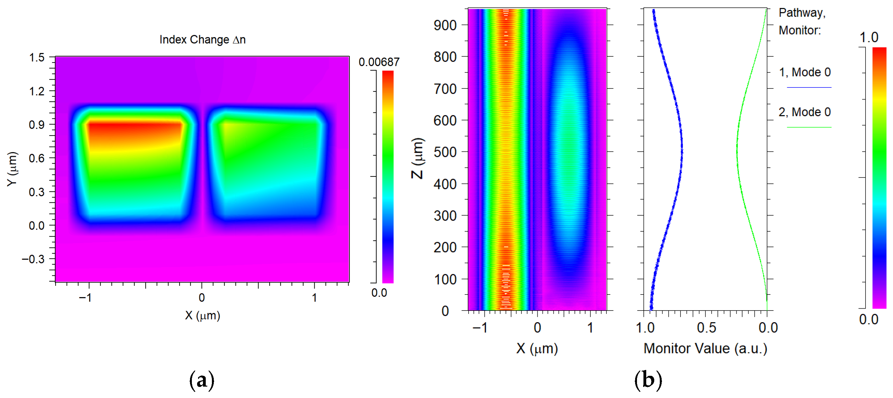
Figure 5a shows the effective-index variation in the heated waveguide and the corresponding thermal crosstalk in the adjacent waveguide.
Figure 5b shows the evolution of optical propagation along the
z-axis at Δ
T = 35 K; the light is confined to the heated guide (bar) as shown on monitor 1 with blue. This yields a basic 2 × 2 block switch; without activating the heater (
T0 = 300 K), the cross state is obtained. When the heater is activated (Δ
T = 35 K), the bar output is obtained. Intermediate temperatures (Δ
T < 35 K) yield partial coupling, enabling power-splitting operation.
3. Shallow-Rib Strip Directional Coupler
One of the main parameters of the coupling level between parallel waveguides is the separation . At small separations, the overlap between the modal tails increases, resulting in stronger coupling. Conversely, as increases, the overlap decreases and the coupling becomes weaker.
The separation between parallel waveguides also influences both dispersion and absorption characteristics, depending on the material filling the gap. Air is commonly employed as the inter-guide medium due to its low refractive index and minimal absorption losses.
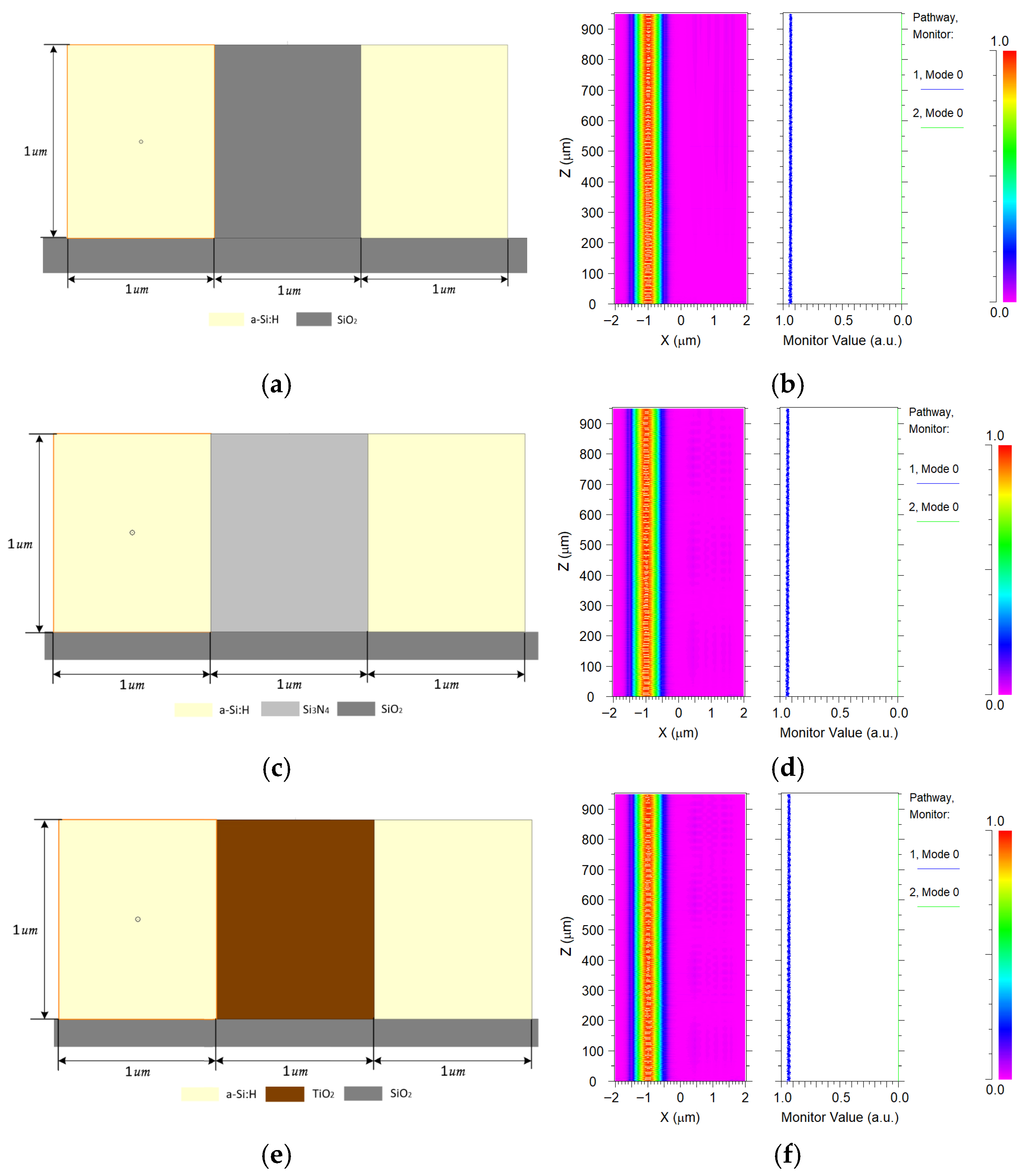
While increasing the refractive index of the gap medium reduces the index contrast with the waveguide core, our simulations indicate that, for moderate-index materials such as SiO
2, Si
3N
4, or TiO
2 [
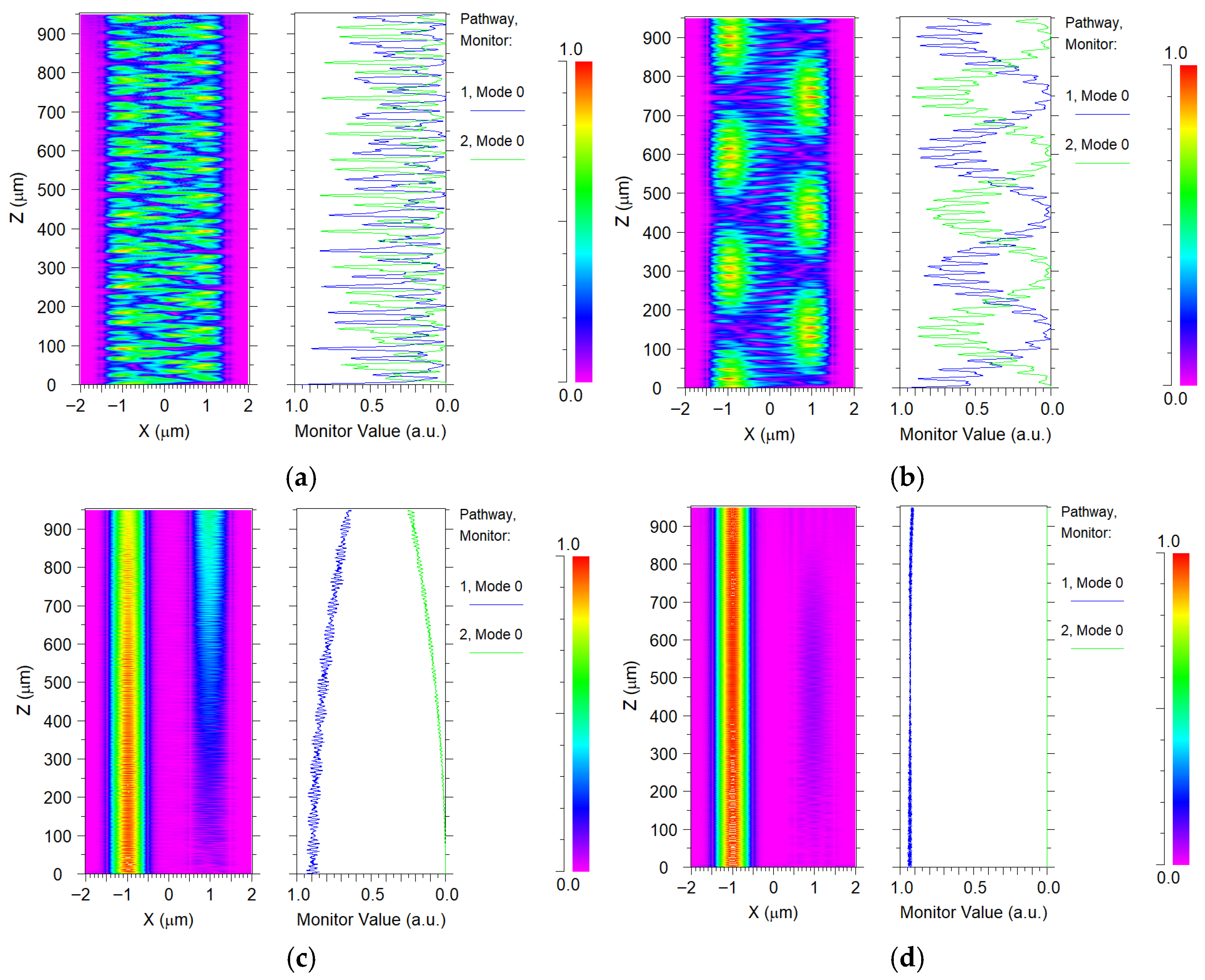
31], no significant optical coupling is observed for a separation of s = 1 μm, as illustrated by the simulations in
Figure 6. In these cases, the index contrast remains sufficiently high to prevent substantial modal overlap between adjacent waveguides.
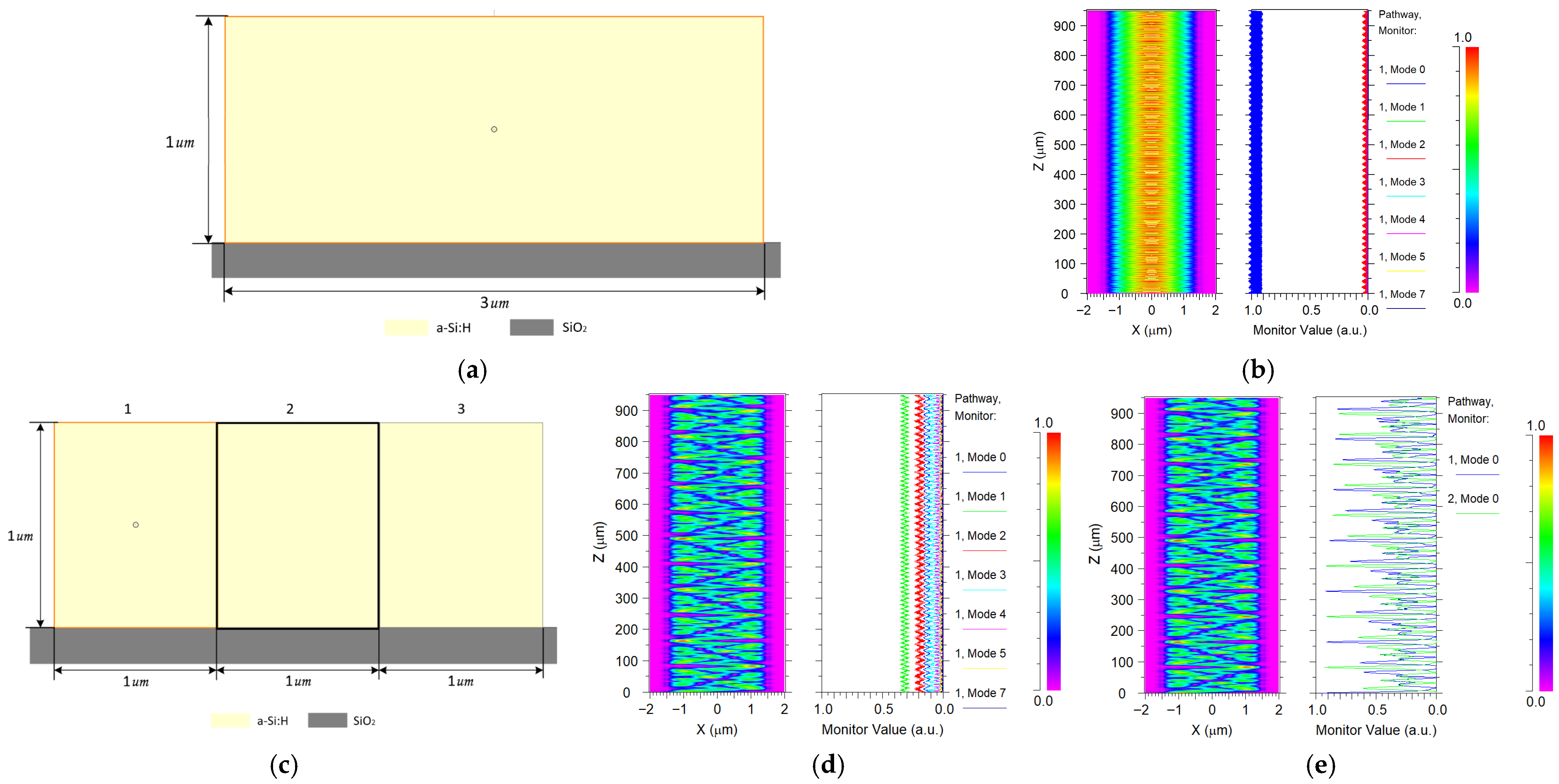
Coupling only becomes apparent when the refractive index of the gap medium approaches that of the a-Si:H core ( = 3.6211 at λ = 1.55 μm). For instance, when the gap index is increased to values around n ≈ 3.2, a slight coupling effect begins to appear due to enhanced modal expansion into the gap region. If the gap were filled with the same a-Si:H material as the waveguides, the two separate cores would effectively merge into a single continuous high-index region, eliminating modal isolation altogether.
In that case, the structure would behave as a wider waveguide (larger
) supporting multiple modes, i.e., operating in the multimode interference (MMI) [
34] regime.
Figure 7a illustrates this transition by replacing the SiO
2 gap in
Figure 6a with a-Si:H. In this merged-core configuration, multimode propagation leads to field redistribution and periodic self-imaging along the propagation direction. This behavior is illustrated in
Figure 7b, which shows the simulated optical field propagation along the
z-axis when the input laser is launched.
In
Figure 7c, the composite waveguide is partitioned into three fixed lateral windows corresponding to the original segments (1–3) previously analyzed in
Figure 6. When the input laser is launched into the first window, the optical propagation is monitored using a modal analysis for transverse-electric (TE) polarization, where seven TE modes are explicitly simulated as shown in
Figure 7d. Due to the waveguide dimensions and its geometrical characteristics, the structure supports multiple guided TE modes, which can be observed propagating along the waveguide.
In
Figure 7e, two mode monitors are placed on segments (1) and (3) of the composite structure shown in
Figure 7c, following the same monitoring approach used in
Figure 6. The analysis focuses on tracking the fundamental TE mode across the monitored segments. The results indicate that the launched TE field is not transferred monotonically to segment (3); instead, the optical power shows a pronounced oscillatory exchange, consistent with multimode beating and incomplete net transfer to the last segment over the considered propagation length.
Taking the results in
Figure 7e as a reference, we analyze the coupling behavior keeping air as the top cladding (cover/insulator) and maintaining the separation between the main waveguides. The study involves gradually reducing the height of the central waveguide segment (3) from
Figure 7c. In this configuration, the optical field remains confined near the bottom of the structure due to the index contrast with the substrate. As the height decreases, the effective index (
) leads to weaker vertical confinement and a lateral broadening of the optical mode within the high-index region where the fundamental TE mode propagates more effectively, as can be seen in
Figure 8. This deconfinement causes the modes of the two parallel guides to have a common slab, and the system diagonalizes into the two supermodes characteristic of the coupled pair (symmetric/antisymmetric) [
28], with effective indices
and
; the modal separation
defines the coupling as
, and
, where L
x is the crossover length (3 dB) in a balanced coupler [
28]. This relationship guides the optimization of the central segment height and waveguide spacing to achieve the desired coupling characteristics.
This analysis also reveals the trade-off between slab height and interaction length: as the height decreases, coupling weakens and a longer interaction length is required. From our study, maintaining the value of
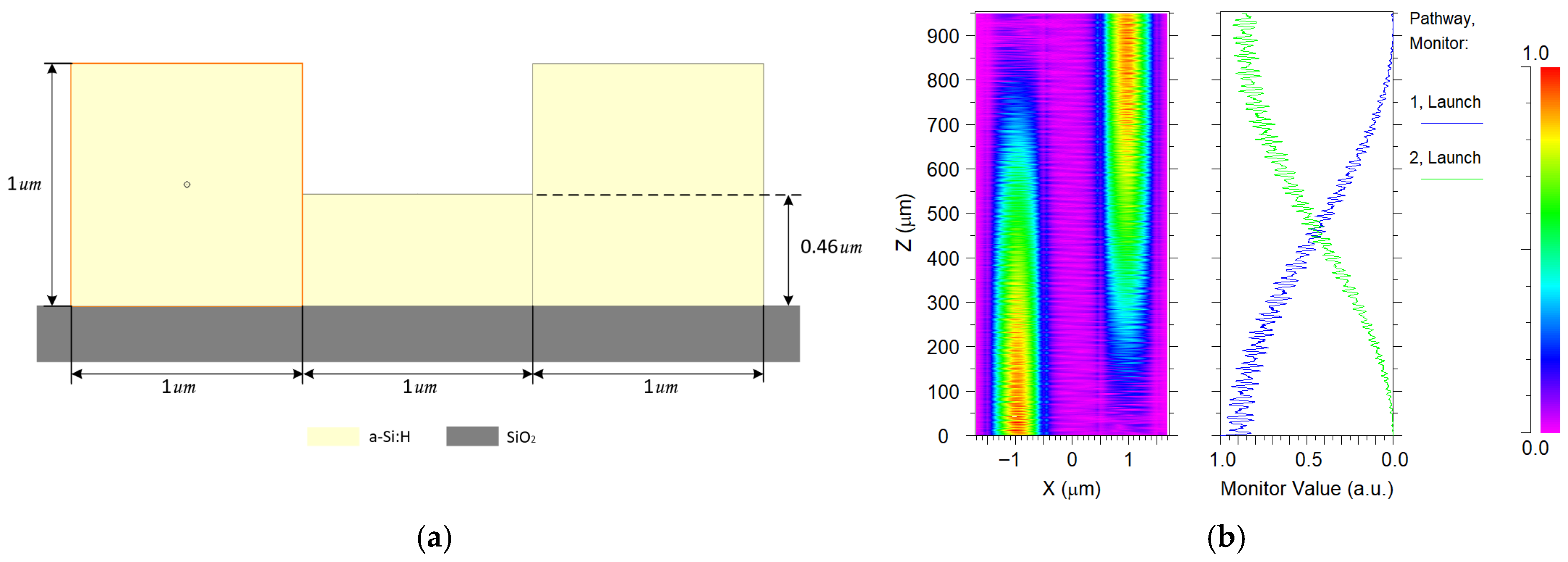
= 950 μm, the optimized height for complete coupling (cross) is
μm, while maintaining
μm. We refer to this configuration as the shallow-rib strip directional coupler, as shown in
Figure 9.
Although the presence of the slab modifies the coupling dynamics, the device operates in the weak-coupling regime and does not function as a multimode interference coupler. The optical field remains primarily confined within the individual waveguide cores, and the coupling mechanism is governed by evanescent interaction, rather than by strong supermode interference or self-imaging effects.
The optical excitation was modeled using RSoft Fiber Mode with an input power of 1 a.u., launched directly into the waveguide input facet. Due to modal overlap between the excitation field and the fundamental TE mode of the 1 × 1 µm a-Si:H waveguide, the effectively coupled power at the device input was 0.85 a.u., corresponding to a launch-related external insertion loss of ILexternal = 0.70 dB measured at the input monitor.
This reduction arises from modal overlap loss under a mode-matched excitation condition. It should therefore not be interpreted as butt-coupling from a standard single-mode fiber (≈10 μm mode field diameter).
All subsequent loss calculations were normalized to the effectively coupled modal power at z = 0 (0.85 a.u.), so that only internal device losses were considered.
The reported internal insertion loss of corresponded to a decrease from 0.85 a.u. at the waveguide entrance to 0.81 a.u. at the output. This attenuation includes all intrinsic propagation and coupling region losses within the device.
The proposed geometry therefore achieves efficient optical transfer with low internal loss (IL < 0.5 dB) for a waveguide separation of s = 1 µm
This type of configuration is particularly advantageous for coupling waveguides separated by distances beyond the range of conventional directional couplers. In advanced platforms, traditional couplers often use S-bends to bring waveguides into nanometric proximity, enabling efficient coupling over a few micrometers; however, such designs require tight lithography and etch control. In contrast, the shallow-rib strip coupler shifts coupling control from lateral separation to the reduced slab height. This enables micrometric gaps and smoother transitions, relaxing lithography, etching requirements, and easing alignment and etch depth tolerances, while maintaining competitive optical performance.
3.1. Thermo-Optic Shallow-Rib Strip Directional Coupler
Using the shallow-rib strip directional coupler shown in
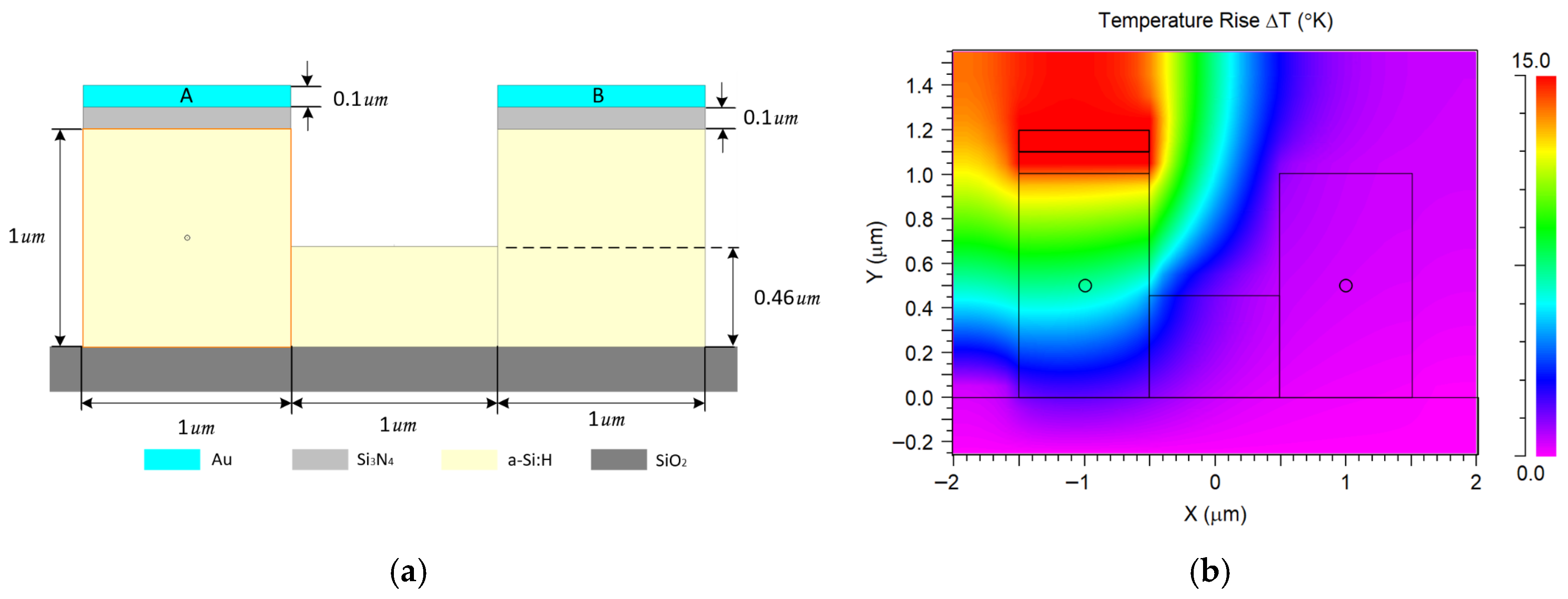
Figure 9a, we will analyze the thermo-optic effect as a control technique, as shown in
Figure 10.
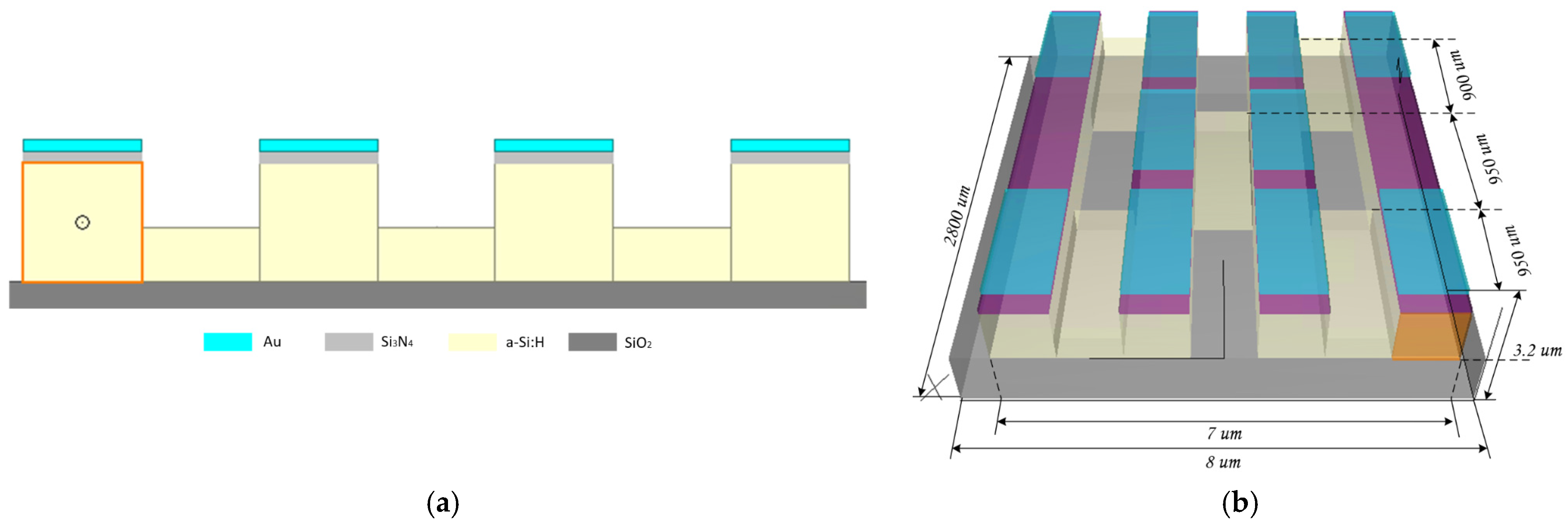
In the thermo-optic shallow-rib strip directional coupler structure shown in
Figure 10a, Au heaters are proposed as the control elements. A heater length of
= 750 μm, centered along the a-Si:H waveguide section, is employed. A Si
3N
4 coating is introduced as an isolation layer, separating the Au heater from the a-Si:H waveguide. This configuration prevents metal-induced optical absorption and suppresses carrier injection and accumulation at the core–heater interface. In addition, due to its higher thermal conductivity compared to SiO
2, the Si
3N
4 layer efficiently channels heat from the metal heater toward the driven waveguide.
Based on the configuration proposed in
Figure 10a, under conditions of total transfer, complete optical coupling is obtained, as illustrated in
Figure 9b for
. To optically confine light within the driven arm, only a temperature increase of 15 K is required at the heater. The resulting thermal profile is shown in
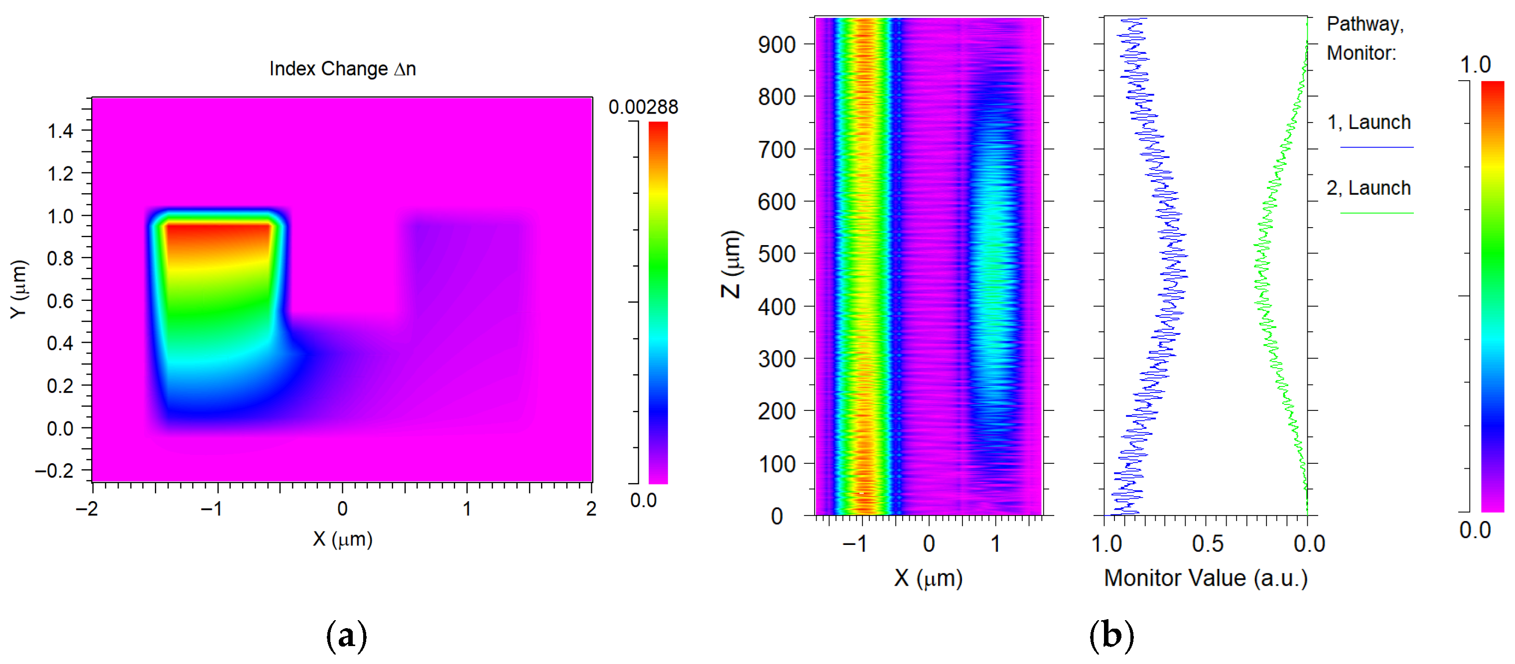
Figure 10b, while the corresponding optical confinement effect is illustrated in
Figure 11b.
From the thermal profile obtained in the simulation, as show in
Figure 10b, a temperature increase of approximately
is observed in the excited waveguide, whereas the neighboring waveguide experiences only a minor temperature rise of
, resulting in a thermal crosstalk value of
.
Figure 11a shows the spatial distribution of the effective-index change induced by the thermo-optic effect for this operating condition at
.
Increasing the distance between the waveguide cores through the slab region, together with the continuous air gap between them, results in a higher lateral thermal resistance, effectively confining heat within the driven arm. Furthermore, since the slab segment is located below the waveguide cores , no continuous high-thermal-conductivity path directly connects the two waveguides, which further suppresses lateral heat conduction. Consequently, the thermal crosstalk metric, , decreases as the waveguide spacing increases, while optical coupling efficiency is preserved through appropriate tuning of the slab height and interaction length.
For the analysis previously presented in
Figure 4 and
Figure 10, we focused on achieving full coupling over a fixed interaction length of L = 950 μm at Δ
T = 0 K. To hold the light in the excited arm under thermal actuation (bar state), the standard directional coupler (DC) exhibited a thermal crosstalk value of
. Under the same optical target and length (but with its own actuation), the shallow-rib strip (SRS) reduced the thermal crosstalk to
. This represents an 85.7% reduction in temperature increase, while requiring much lower temperatures to achieve the same result; in other words, the shallow-rib strip configuration is approximately seven times more efficient in mitigating temperature rise.
3.2. The 4 × 4 Thermo-Optic Programmable Photonic Matrix Based on Amorphous Silicon
Using the thermo-optic shallow-rib strip directional coupler defined in
Figure 11 as the fundamental 2 × 2 block,
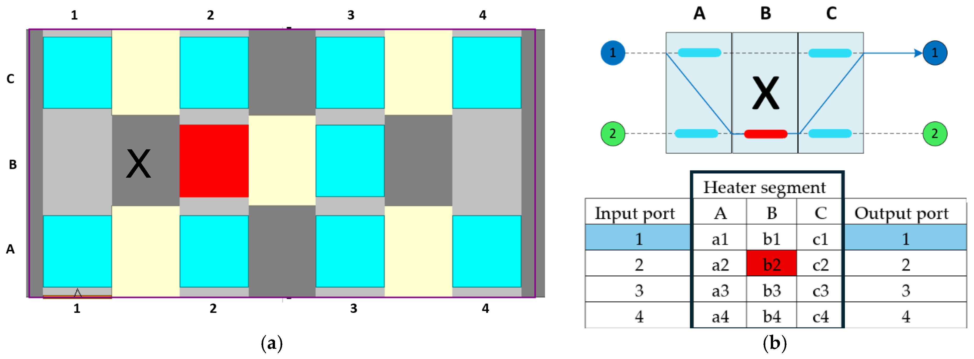
Figure 12 shows the 4 × 4 thermo-optic programmable photonic matrix based on amorphous silicon.
The materials used in the structure are color-coded as follows: cyan represents the gold (Au) heaters used for thermo-optic tuning; light gray corresponds to the silicon nitride (Si3N4) passivation layer in 3D (light purple); light yellow indicates the a-Si:H waveguide core; and dark gray (base) denotes the SiO2 substrate.
The matrix shown in
Figure 12b is designed to reduce the number of active elements (heaters) to control the outputs based on the input without using S-bends as connecting elements between the couplers. This compact structure has dimensions of 8 μm × 2800 μm, consisting of three segments on the horizontal (
x-axis) with lengths
=
= 950 μm and
= 900 μm.
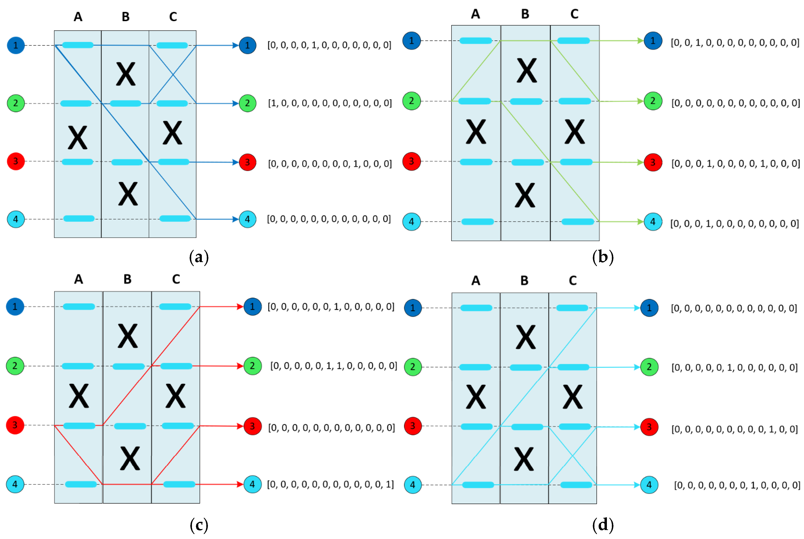
When no control element is activated in the shallow-rib strip coupler, the light into one guide is completely transferred to the unexcited parallel guide, and so the default output corresponds to the cross port. By activating the heaters, the light is confined to the activated segment. The state map shown in
Figure 13 shows the heaters that need to be activated for each input/output combination.
As shown in
Figure 13 and
Figure 14, there is a gap between the coupler modules; this refers to areas without coupling. These positions are labeled with the symbol “X” in
Figure 14. This layout avoids the use of S-bends, reducing device length, mask complexity, and bending-related losses. By using straight sections and controlled couplers only, the circuit is more compact and less sensitive to lithography and alignment errors than conventional curved interconnections.
The a × b nomenclature is used to specify a particular input/output configuration, where a denotes the selected input port and b indicates the desired output port. In the context of a matrix with four output ports per input, this is represented as a × 4, where a represents the active input port for their four outputs, with the matrix being 1 × 4 (one input and four outputs). Thus, for example in a 1 × 4 matrix, directing the input signal to output port number 3 is denoted as 1 × 3. Similarly, routing to port 1, 2, or 4 would be referred to as 1 × 1, 1 × 2, or 1 × 4, respectively.
To represent the switching elements using the physical locations of the heaters, a 4 × 3 logic control matrix is used, where each row corresponds to an output port, numbered from 1 to 4, and each column corresponds to one of the three heater segments labeled [A, B, C], as shown in
Table 1. Each element in the matrix (a, b, c) takes a binary value: 1 indicates that the heater is activated in that specific segment, while 0 denotes an inactive (default) state. This representation is used in
Figure 14. This abstraction allows for a compact and programmable representation of the switching configuration for each output path.
As shown in
Figure 13a, in the 1 × 4 matrix configuration, the optical signal is launched into input port 1, and one of the four available output ports can be selected.
For the specific case of the 1 × 1 configuration within the 1 × 4 matrix,
Figure 14 illustrates the switching process. When optical signal is launched to guide 1, the signal propagates and couples to guide 2 until the total transfer of optical light to the second guide is enhanced, as the electrodes in a1 or a2 are not activated. When the heater at position b2 is activated, it confines the light within that segment. Due to the default design of the structure, the light then continues toward segment c2, where the heater is inactive. This absence of activation allows the light to be optically transferred to adjacent segment c1, and finally to output port 1.
The heater is driven by a rectangular pulse delivering constant power, modeled as a DC step during the active interval. The pulse duration is defined by the thermal time constant
, where
represents the heat capacity of the heated waveguide section and
is the thermal conductance to the surrounding environment [
9]. In programmable photonic arrays, pulse width modulation (PWM) is commonly used to control the average power delivered to the heaters, enabling precise tuning of the phase shift while preserving the thermal bandwidth constraints [
21,
35].
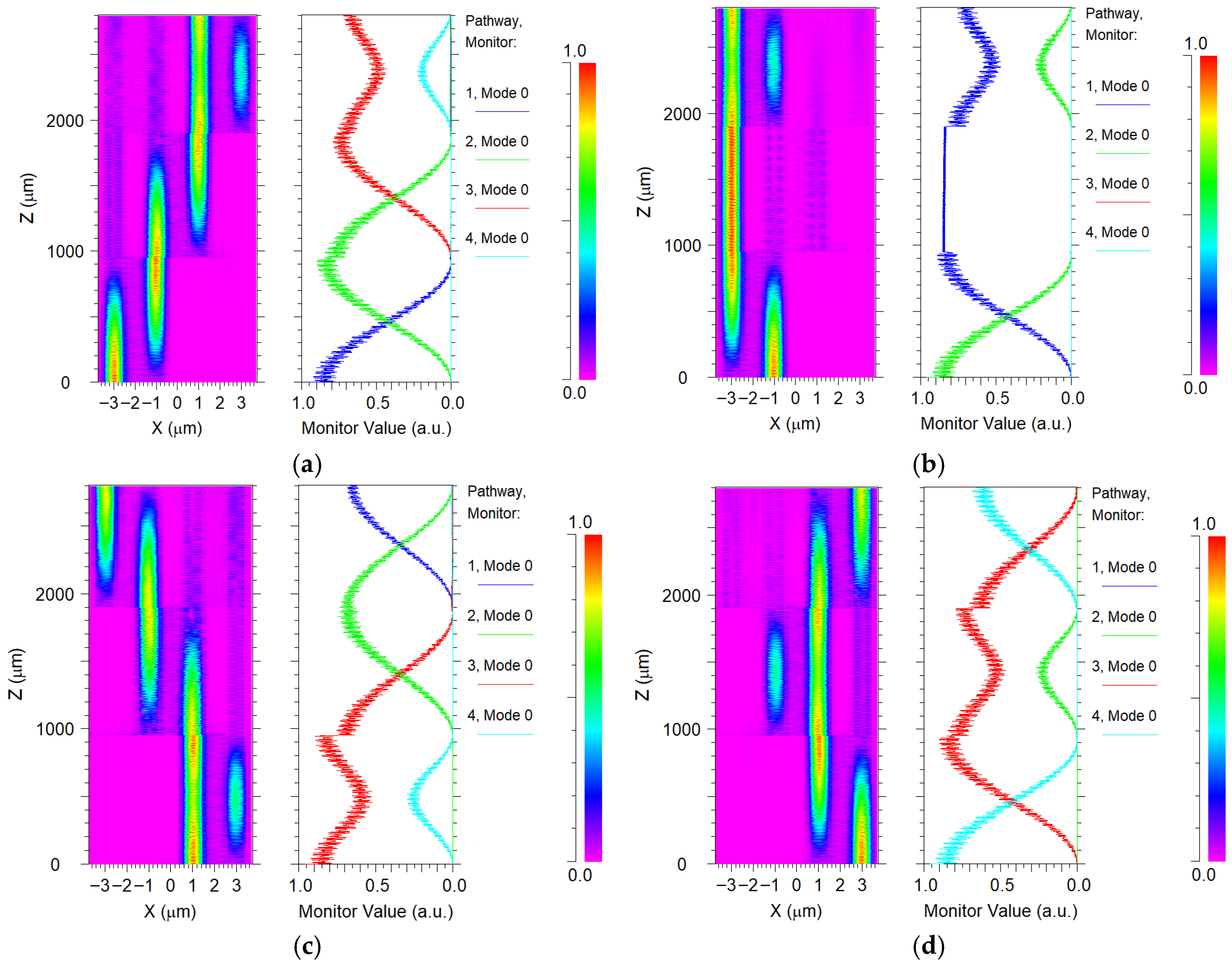
We analyze the results obtained through simulations in the BeamPROP tool. Since a full set of 16 input/output configurations is available,
Figure 15 reports representative cases for each input for clarity. As mentioned above, the fundamental block has an external insertion loss of
. One way to mitigate this insertion loss is to include a fiber-to-chip coupling stage, such as an on-chip grating coupler [
36]. Another solutions is to introduce an adiabatic taper or spot-size converter that gradually widens the core to 3–4 µm before the functional section. In this way, the optical field is still confined in the fundamental mode, and its transverse profile widens smoothly, gradually matching its shape and numerical aperture to those of the fiber or external source. The result is greater modal overlap, which in theory should reduce insertion loss to <0.2 dB [
37,
38].
Another probable problem is due to reflection, given that the air interface and in the a-Si:H waveguide, . The normal reflection obtained from our data is R = 0.322, which means that the a-Si:H waveguide may reflect approximately 32.2% of the incident power.
An effortless way to mitigate these losses using materials and processes compatible with CMOS technology is to deposit a thin Anti-Reflective (AR) film with an intermediate index on the facet or on the grating coupler itself. The ideal index is . Standard materials are Si3N4 (n ≈ 2.0) or SiOxNγ (n ≈ 1.9). If the film thickness is adjusted to λ/4 at the operating wavelength of 1.55 µm, destructive interference occurs in the reflected wave, reducing the reflectance to below 0.5% (<0.05 dB). This improves the link’s power budget and prevents optical feedback to the source.
In our 4 × 4 design, to mitigate edge-coupling reflections, we applied an AR coating to the chip facet at the entrance of the a-Si:H waveguide array (we did not use grating couplers). In our simulations, a quarter-wavelength AR coating optimized for the refractive index of a-Si:H at 1.55 µm using a Si3N4 film thickness of approximately 0.2 µm resulted in negligible insertion loss (IL) variation. Thicker films, however, degraded IL due to deviation from the λ/4 condition.
In
Figure 15, several monitors are placed along each waveguide segment corresponding to the different channels in order to track the energy transfer of the fundamental TE mode (mode 0) along the propagation direction. The blue color represents the first waveguide, the green the second waveguide, the red the third waveguide, and the cyan curve the fourth waveguide. The color convention is consistent with that used in
Figure 13 for clarity and direct comparison between configurations.
As shown in
Figure 15c,d, the abrupt changes observed in red curves correspond to the moment when the dominant modal power transfers from the heated waveguide (with higher effective index) to the adjacent unheated guide. In contrast, in segments without thermal actuation (e.g., segment 2b in
Figure 14b), the mode remains well confined and propagates similarly to an isolated waveguide, resulting in a continuous evolution without pronounced coupling effects.
In terms of optical power, the simulated values obtained for each input–output port combination of the 4 × 4 matrix are summarized in
Table 2. The reference launch power used for normalization is 0.85 a.u., corresponding to the effective power coupled into the input waveguide in the simulation.