Simulations and Experiments on Activation of Doped Silicon Wafers Based on Dual Beam of 785 nm Semiconductor Laser and 10.6 μm CO2 Laser

 , ,
, ,
Abstract
1. Introduction
2. Theory and Model
2.1. Theoretical Principles
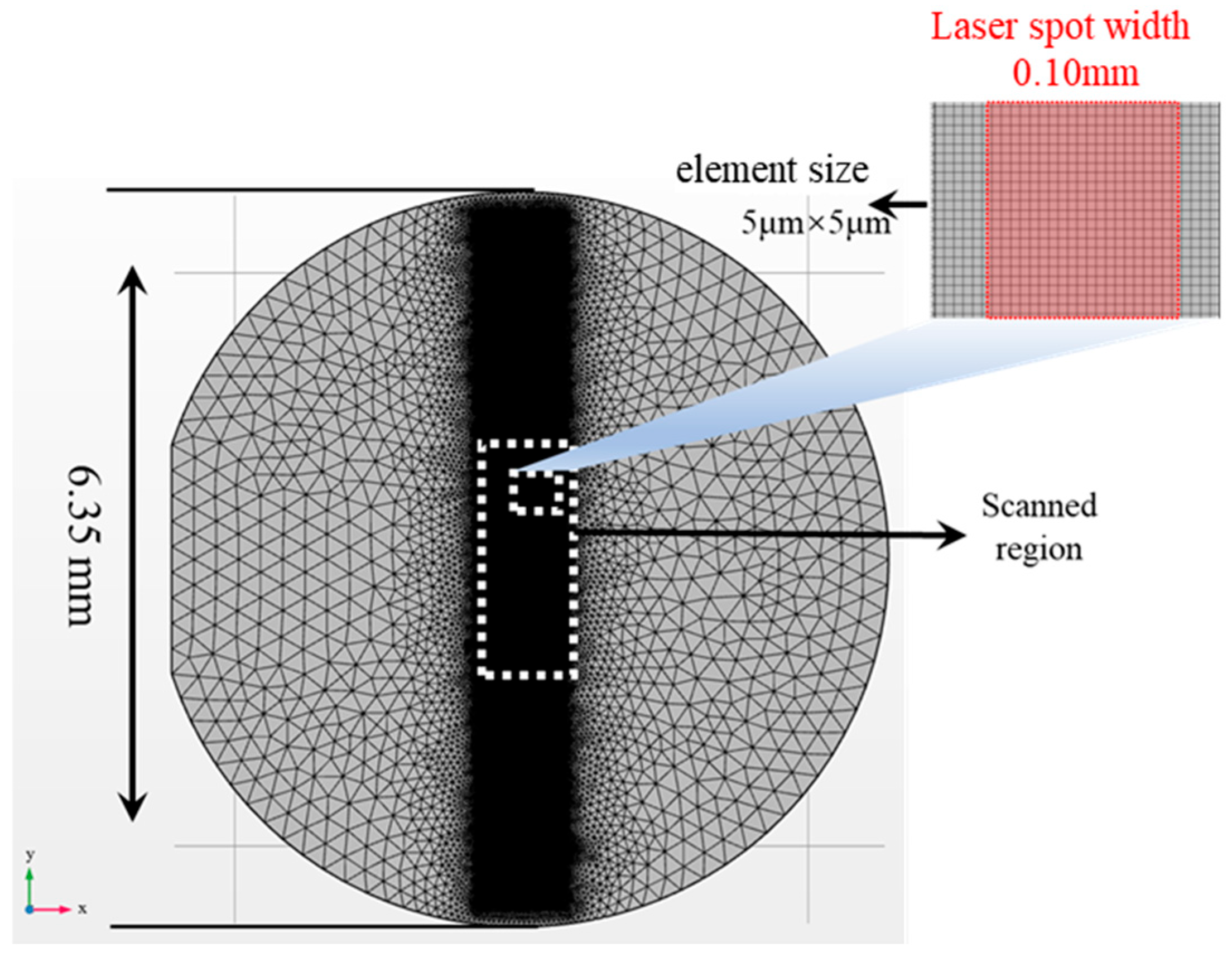
2.2. Selection of Computational Domain and Parameter Settings
2.3. Model Establishment and Simulation Analysis
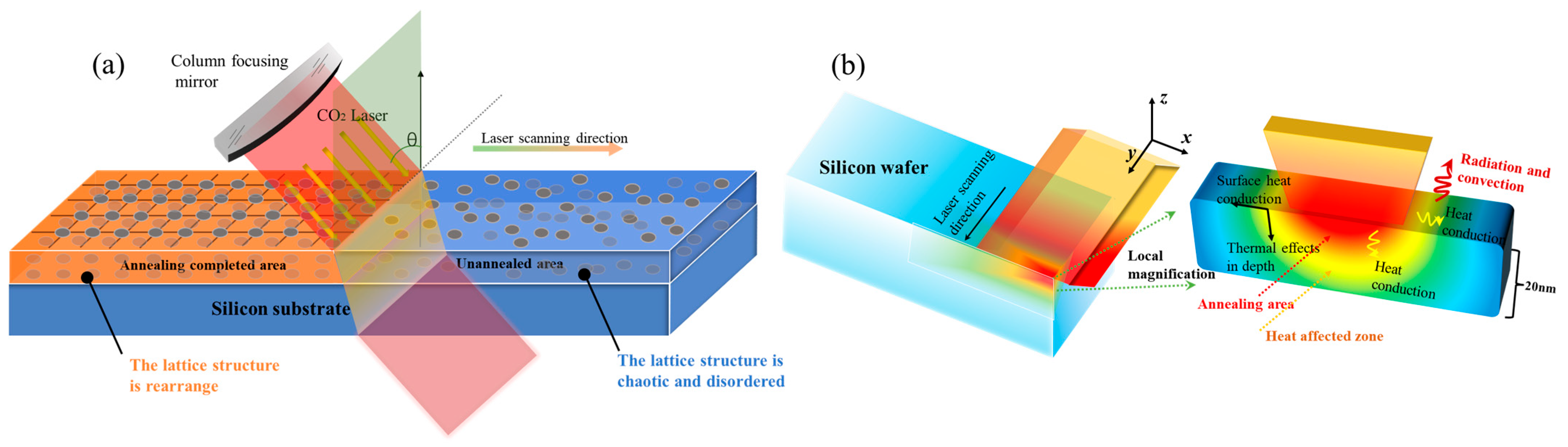
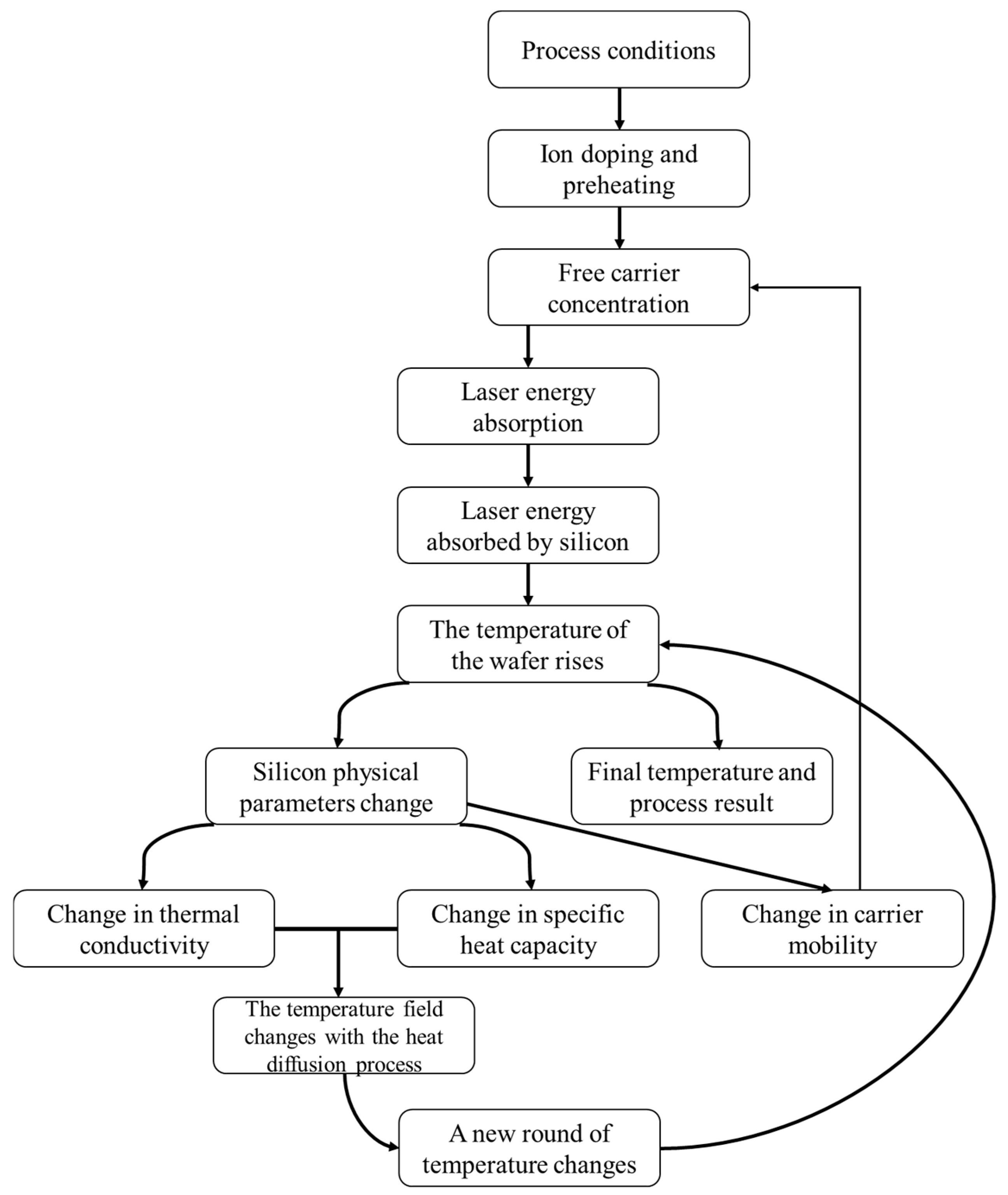
2.3.1. Physical Process
2.3.2. Thermal Control Equation
2.3.3. Laser Scanning Motion and Model Boundaries
2.3.4. Modeling of the Material Absorption Coefficient
2.3.5. Dopant Concentration Profile
2.3.6. Thermal Stress Deformation
2.4. Experimental Equipment and Annealing Effect Characterization Methods
3. Results and Discussion
3.1. Validation of Simulation Results
3.2. Influence of Process Parameters on Annealing Temperature Distribution
3.2.1. Annealing Laser Power Density
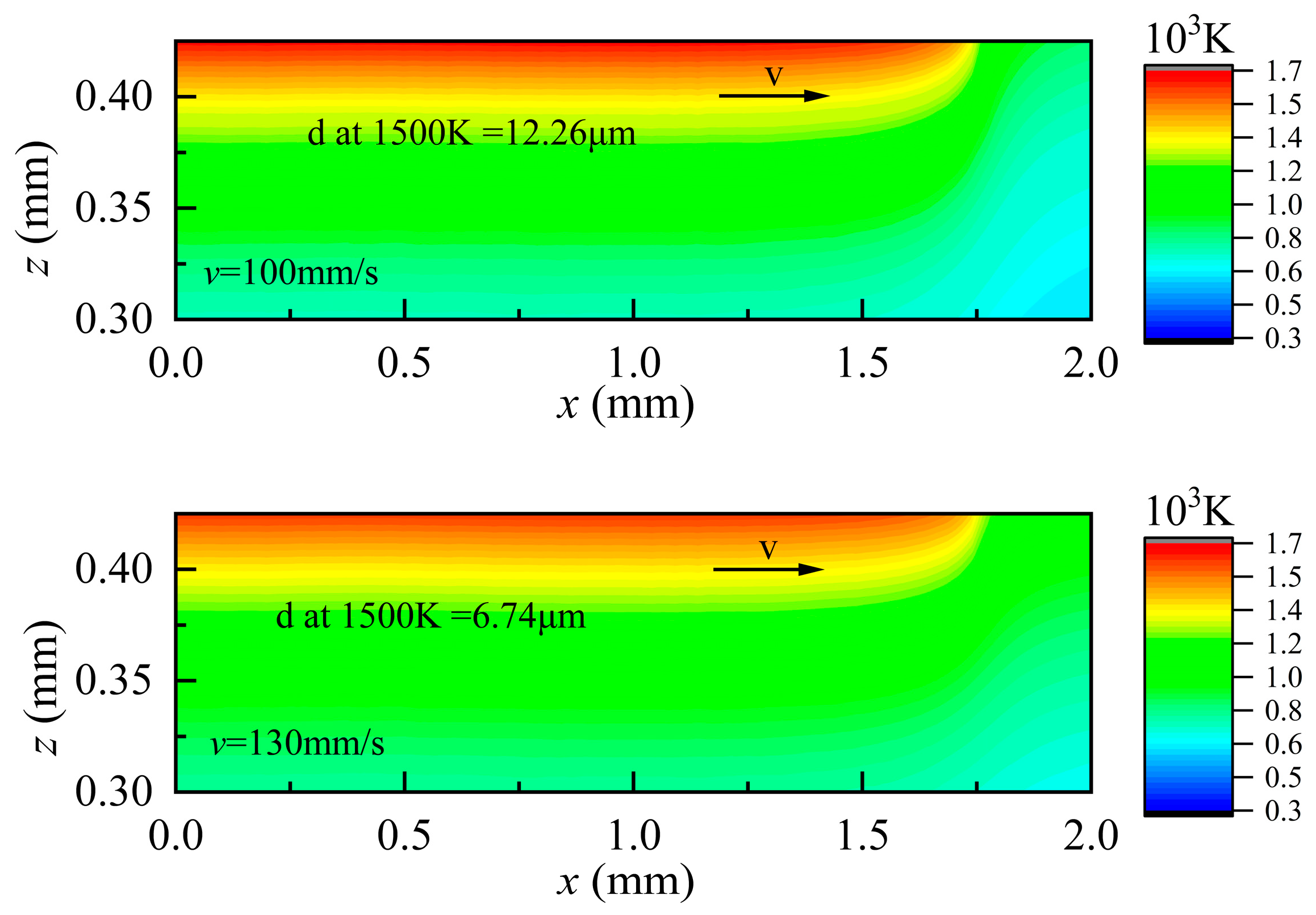
3.2.2. Beam Scanning Speed
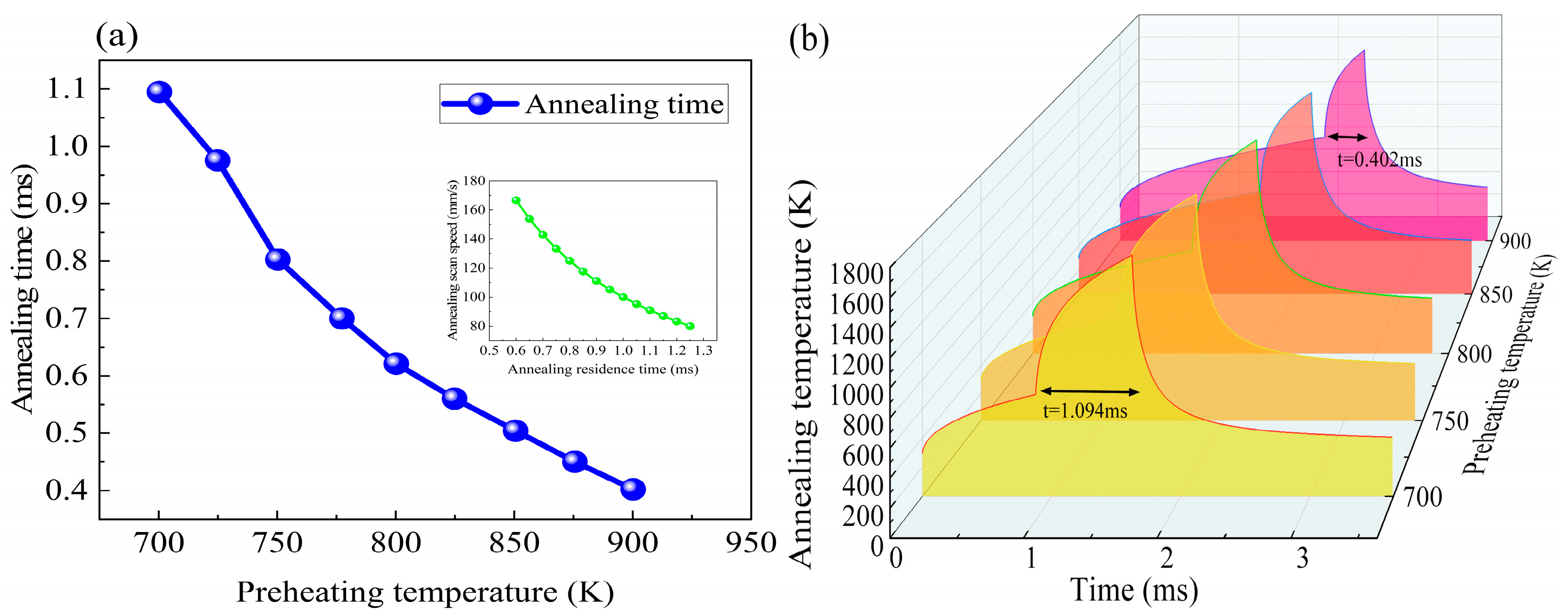
3.2.3. Preheating Temperature
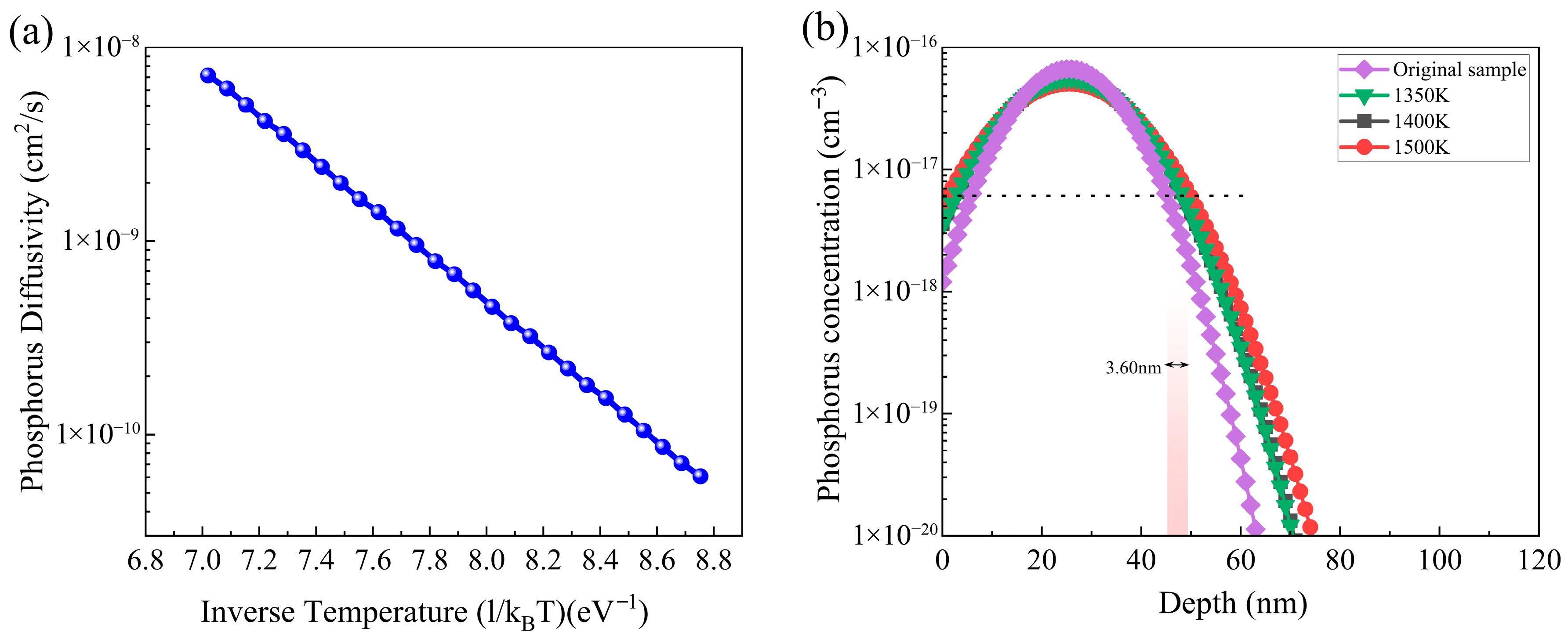
3.2.4. Dopant Diffusion Extent
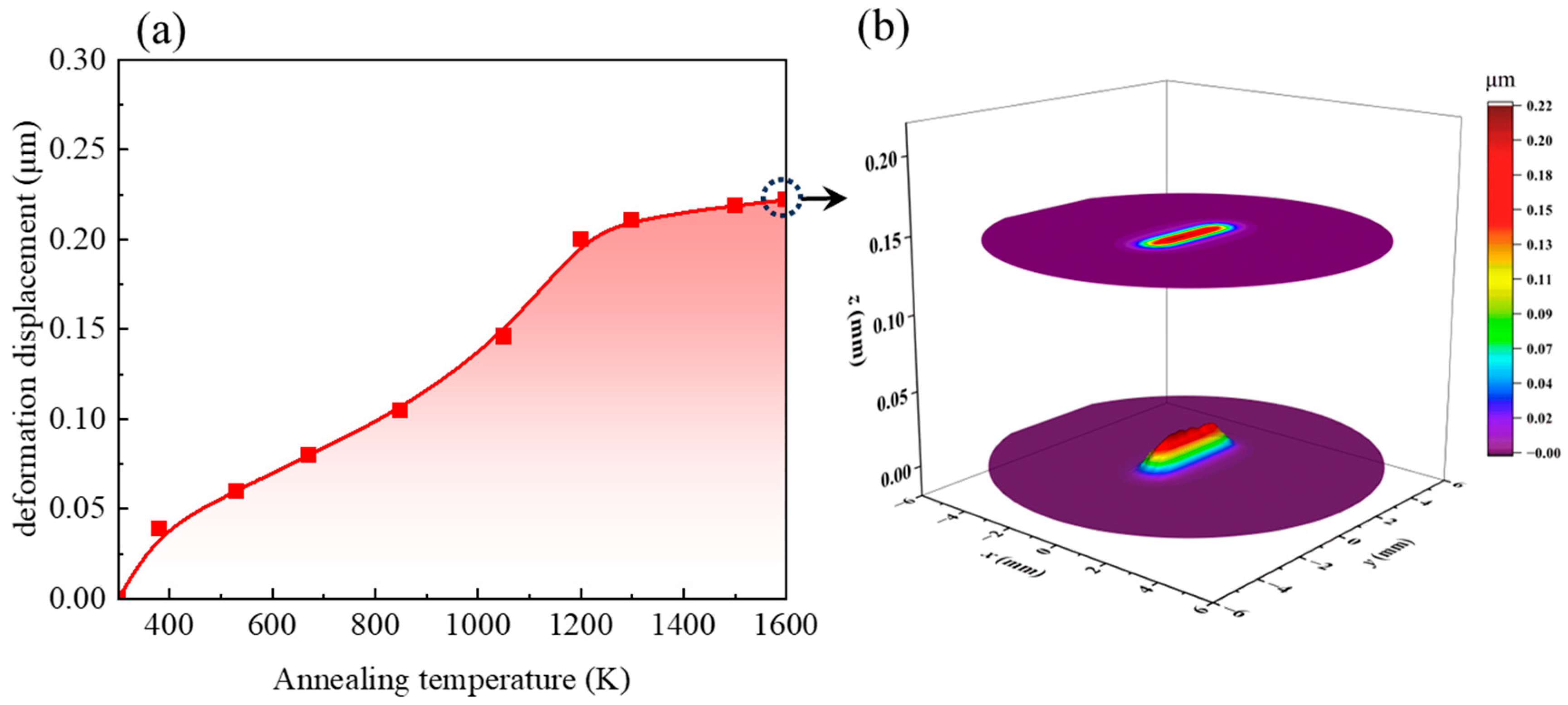
3.2.5. Thermal Stress Deformation Analysis
4. Discussion
5. Conclusions
Author Contributions
Funding
Data Availability Statement
Conflicts of Interest
References
- Feng, P.; Song, S.C.; Nallapati, G.; Zhu, J.; Bao, J.; Moroz, V.; Chidambaram, C. Comparative analysis of semiconductor device architectures for 5-nm node and beyond. IEEE Electron Device Lett. 2017, 38, 1657–1660. [Google Scholar] [CrossRef] [Scilit]
- Kingi, R.; Wang, Y.; Fonash, S.J.; Awadelkarim, O.; Mehlhaff, J. Comparison Between Rapid Thermal and Furnace Annealing for A-Si Solid Phase Crystallization. Mater. Res. Soc. Symp. Proc. 1994, 345, 375–380. [Google Scholar] [CrossRef] [Scilit]
- Yu, N.; Kaminer, I.; Kheifets, R.; Yan, X.; Yang, F.; Joannopoulos, J.D.; Soljačić, M. Coherent Surface Plasmon Polariton Amplification via Free-Electron Pumping. Nature 2022, 611, 55–60. [Google Scholar] [CrossRef] [Scilit]
- Gargini, P.A. The IRDS Is Paving the Way for Chips Acts around the World. In Proceedings of the International Conference on Extreme Ultraviolet Lithography 2023, Monterey, CA, USA, 1–5 October 2023; SPIE: Bellingham, WA, USA, 2023; Volume PC12750, pp. 15–29. [Google Scholar]
- Huang, Y.J.; Liu, C.C.; Lo, K.Y.; Chu, S.Y. Controlling Surface Shallow Junction Depth by a Rapid Thermal Annealing Process with Low Ambient Pressure. Appl. Surf. Sci. 2011, 257, 2494–2497. [Google Scholar] [CrossRef] [Scilit]
- Jung, S.M.; Park, C.J.; Jeong, H.; Shin, M.W. Effect of Number of Laser Pulses on p/n Silicon Ultra-Shallow Junction Formation during Non-Melt Ultra-Violet Laser Thermal Annealing. Mater. Sci. Semicond. Process. 2017, 60, 34–39. [Google Scholar] [CrossRef] [Scilit]
- Gunawan, R.; Jung, M.Y.L.; Seebauer, E.G.; Braatz, R.D. Optimal Control of Rapid Thermal Annealing in a Semiconductor Process. J. Process Control 2004, 14, 423–430. [Google Scholar]
- Aziz, M.; Felix, J.F.; Jameel, D.; Al Saqri, N.; Al Mashary, F.S.; Alghamdi, H.M.; Albalawi, H.M.A.; Taylor, D.; Henini, M. Rapid Thermal Annealing: An Efficient Method to Improve the Electrical Properties of Tellurium Compensated Interfacial Misfit GaSb/GaAs Heterostructures. Superlattices Microstruct. 2015, 88, 80–89. [Google Scholar] [CrossRef] [Scilit]
- Makarevich, Y.V.; Komarov, F.F.; Komarov, A.F.; Mironov, A.M.; Zayats, G.M.; Miskevich, S.A. Controlling Boron Diffusion during Rapid Thermal Annealing with Co-Implantation by Amphoteric Impurity Atoms. Bull. Russ. Acad. Sci. Phys. 2012, 76, 574–576. [Google Scholar] [CrossRef] [Scilit]
- Mileham, J.; Willis, J.; Owen, D.M.; Shetty, S.; Hebb, J.; Wang, Y. Impact of Pattern and LSA Stitching Effects and Processing Parameters on Reflectance and Stress Distribution for Thermal Annealing Technologies. In Proceedings of the 2009 17th International Conference on Advanced Thermal Processing of Semiconductors—RTP 2009, Albany, NY, USA, 29 September–2 October 2009; IEEE: Piscataway, NJ, USA, 2009; pp. 1–6. [Google Scholar]
- Shanks, H.R.; Maycock, P.D.; Sidles, P.H.; Danielson, G.C. Thermal Conductivity of Silicon from 300 to 1400 K. Phys. Rev. 1963, 130, 1743–1748. [Google Scholar]
- Yu, X.Q.; Zeng, Y.-S.; Song, L.W.; Kong, D.Y.; Hao, S.B.; Gui, J.Y.; Yang, X.J.; Xu, Y.; Wu, X.J.; Leng, Y.X.; et al. Megaelectronvolt Electron Acceleration Driven by Terahertz Surface Waves. Nat. Photonics 2023, 17, 957–963. [Google Scholar]
- Chen, Y.; Cheng, Y.; Zhu, R.; Wang, F.; Cheng, H.; Liu, Z.; Fan, C.; Xue, Y.; Yu, Z.; Zhu, J.; et al. Nanoscale All-Optical Logic Devices. Sci. China-Phys. Mech. Astron. 2018, 61, 114231. [Google Scholar] [CrossRef] [Scilit]
- Timans, P.; Gelpey, J.; McCoy, S.; Lerch, W.; Paul, S. Millisecond Annealing: Past, Present and Future. Mater. Res. Soc. Symp. Proc. 2005, 912, C01. [Google Scholar] [CrossRef] [Scilit]
- Huet, K.; Mazzamuto, F.; Tabata, T.; Toque-Tresonne, I.; Mori, Y. Doping of Semiconductor Devices by Laser Thermal Annealing. Mater. Sci. Semicond. Process. 2017, 62, 92–102. [Google Scholar] [CrossRef] [Scilit]
- Reichel, D.; Lerch, W.; Paul, S.; Niess, J.; Cristiano, F.; Severac, F.; Gavelle, M.; Boninelli, S.; De Salvador, D.; Napolitani, E.; et al. Precise Millisecond Annealing for Advanced Material Processing. Phys. Status Solidi C 2012, 9, 2008–2012. [Google Scholar] [CrossRef] [Scilit]
- Prucnal, S.; Rebohle, L.; Skorupa, W. Doping by Flash Lamp Annealing. Mater. Sci. Semicond. Process. 2017, 62, 115–127. [Google Scholar] [CrossRef] [Scilit]
- Foggiato, J.; Yoo, W.S. Millisecond Flash Annealing: Applications for USJ Formation and Optimization of Device Electrical Characteristics. Mater. Sci. Eng. B 2005, 124–125, 219–222. [Google Scholar] [CrossRef] [Scilit]
- Smith, M.P.; Seffen, K.A.; McMahon, R.A.; Voelskow, M.; Skorupa, W. Analysis of Wafer Stresses during Millisecond Thermal Processing. J. Appl. Phys. 2006, 100, 033509. [Google Scholar] [CrossRef] [Scilit]
- Zhang, D.; Zeng, Y.; Tian, Y.; Li, R. Coherent Free-Electron Light Sources. Photonics Insights 2023, 2, R07. [Google Scholar] [CrossRef] [Scilit]
- Li, J.; Wang, L.; Xu, X.; Lei, K.; Tang, B.; Dai, H.; Zhang, J.; Jian, J.; Ye, Y.; Ma, H.; et al. Local Laser Annealing for Amorphous/Polycrystalline Silicon Hybrid Photonics on CMOS. Opt. Laser Technol. 2025, 181, 111799. [Google Scholar] [CrossRef] [Scilit]
- Baik, S.; Kwon, D.-J.; Kang, H.; Jang, J.E.; Jang, J.; Kim, Y.S.; Kwon, H.-J. Conformal and Ultra-Shallow Junction Formation Using a Pulsed-Laser Annealing Process Integrated with a Modified Plasma Assisted Doping Method. IEEE Access 2020, 8, 172166–172174. [Google Scholar] [CrossRef] [Scilit]
- Noda, T.; Felch, S.; Parihar, V.; Vrancken, C.; Janssens, T.; Bender, H.; Vandervorst, W. Modeling and Experiments of Boron Diffusion during Sub-Millisecond Non-Melt Laser Annealing in Silicon. Mater. Res. Soc. Symp. Proc. 2006, 912, C05–C06. [Google Scholar] [CrossRef] [Scilit]
- Huang, W.-H.; Shieh, J.-M.; Kao, M.-H.; Shen, C.-H.; Huang, T.-E.; Wang, H.-H.; Yang, C.-C.; Hsieh, T.-Y.; Hsieh, J.-L.; Yu, P.; et al. Enabling N-Type Polycrystalline Ge Junctionless FinFET of Low Thermal Budget by in Situ Doping and Visible Pulsed Laser Annealing. Appl. Phys. Express 2017, 10, 026502. [Google Scholar] [CrossRef] [Scilit]
- Wang, H.T.; Tan, L.S.; Chor, E.F. Pulsed Laser Annealing of Be-Implanted GaN. J. Appl. Phys. 2005, 98, 083538. [Google Scholar] [CrossRef] [Scilit]
- Cacho, F.; Bono, H.; Beneyton, R.; Dumont, B.; Colin, A.; Morin, P. Simulation of Pattern Effect Induced by Millisecond Annealing Used in Advanced Metal-Oxide-Semiconductor Technologies. J. Appl. Phys. 2010, 108, 013510. [Google Scholar] [CrossRef] [Scilit]
- Jin, S.; Hong, S.; Mativenga, M.; Kim, B.; Shin, H.H.; Park, J.K.; Kim, T.-W.; Jang, J. Low-Temperature Polycrystalline Silicon with Single Orientation on Glass by Blue Laser Annealing. Thin Solid Film. 2016, 616, 838–841. [Google Scholar] [CrossRef] [Scilit]
- Zhou, S.; Bai, Y.; Yu, J.; Zhang, Z.; Li, Y.; Zhang, J.; Zhang, Z.; Zhu, B.; He, M.; Teng, J.; et al. Self-Organized Kilotesla Magnetic-Tube Array in an Expanding Spherical Plasma Irradiated by kHz Femtosecond Laser Pulses. Phys. Rev. Lett. 2018, 121, 255002. [Google Scholar] [CrossRef] [Scilit]
- Bai, Y.; Zhou, S.; Yu, J.; Zhang, Z.; Li, Y.; Zhang, J.; Zhang, Z.; Zhu, B.; He, M.; Teng, J.; et al. Observation of Subrelativistic Collisionless Shocks Generation and Breakout Dynamics. Nat. Commun. 2025, 16, 3770. [Google Scholar] [CrossRef] [Scilit]
- Wang, Y.; Chen, S.; Shen, M.; Wang, X.; Zhou, S.; Hebb, J.; Owen, D. Dual Beam Laser Spike Annealing Technology. In Proceedings of the 2010 International Workshop on Junction Technology, Shanghai, China, 10–11 May 2010; IEEE: Piscataway, NJ, USA, 2010; pp. 1–6. [Google Scholar]
- Huet, K.; Aubin, J.; Raynal, P.-E.; Curvers, B.; Verstraete, A.; Lespinasse, B.; Mazzamuto, F.; Sciuto, A.; Lombardo, S.F.; La Magna, A.; et al. Pulsed Laser Annealing for Advanced Technology Nodes: Modeling and Calibration. Appl. Surf. Sci. 2020, 505, 144470. [Google Scholar] [CrossRef] [Scilit]
- Colin, A.; Morin, P.; Cacho, F.; Bono, H.; Beneyton, R.; Bidaud, M.; Mathiot, D.; Fogarassy, E. Simulation of the Sub-Melt Laser Anneal Process in 45 nm CMOS Technology—Application to the Thermal Pattern Effects. Mater. Sci. Eng. B 2008, 154–155, 31–34. [Google Scholar] [CrossRef] [Scilit]
- Iyengar, K.A.; Clancy, P.; Thompson, M. A 3D Model for Simulating Temperature and Stress Profiles during Sub-Millisecond Laser Spike Annealing. In Proceedings of the 2010 18th International Conference on Advanced Thermal Processing of Semiconductors (RTP), Portland, OR, USA, 28 September–1 October 2010; IEEE: Piscataway, NJ, USA, 2010; pp. 90–96. [Google Scholar]
- Jennings, D.; Mayur, A.; Parihar, V.; Liang, H.; Mcintosh, R.; Thomas, T.; Ranish, J.; Hunter, A.; Trowbridge, T.; Achutharaman, R.; et al. Dynamic Surface Anneal: Activation without Diffusion. In Proceedings of the 12th IEEE International Conference on Advanced Thermal Processing of Semiconductors, RTP 2004, Portland, OR, USA, 29 September–2 October 2004; IEEE: Piscataway, NJ, USA, 2004; pp. 47–51. [Google Scholar]
- Tsai, C.-Y. Absorption Coefficients of Silicon: A Theoretical Treatment. J. Appl. Phys. 2018, 123, 183103. [Google Scholar] [CrossRef] [Scilit]
- Florian, C.; Fischer, D.; Freiberg, K.; Duwe, M.; Sahre, M.; Schneider, S.; Hertwig, A.; Krüger, J.; Rettenmayr, M.; Beck, U.; et al. Single Femtosecond Laser-Pulse-Induced Superficial Amorphization and Re-Crystallization of Silicon. Materials 2021, 14, 1651. [Google Scholar] [CrossRef] [Scilit] [PubMed]
- Cristiano, F.; Fuccio, F.; Severac, F.; Lerch, W. Defect Evolution and Dopant Activation in Laser Annealed Si and Ge. Mater. Sci. Semicond. Process. 2016, 42, 188–195. [Google Scholar] [CrossRef] [Scilit]
- Baeri, P.; Campisano, S.U.; Foti, G.; Rimini, E. Pulsed Laser Heating of Silicon: The Coupling of Optical Absorption and Thermal Conduction during Irradiation. J. Appl. Phys. 1983, 54, 366–372. [Google Scholar] [CrossRef] [Scilit]
- He, Z. Analysis on the Development of Semiconductor Manufacturing Process. J. Phys. Conf. Ser. 2022, 2295, 012009. [Google Scholar] [CrossRef] [Scilit]
- Green, M.A. Optical Properties of Intrinsic Silicon at 300 K. Prog. Photovolt. 1995, 3, 189–192. [Google Scholar] [CrossRef] [Scilit]
- Schumann, T.; Abbadie, A.; Hartmann, J.M.; Buca, D.; Mantl, S.; Tillack, B.; Zhao, Q.T. Near-Infrared Free Carrier Absorption in Heavily Doped Silicon. J. Appl. Phys. 2014, 116, 063106. [Google Scholar] [CrossRef] [Scilit]
- Mayer, J.W.; Marsh, O.J.; Baron, R.; Shifrin, G.A.; Kahn, B. Ion Implantation in Semiconductors—Part I: Range Distribution Theory and Experiments. Proc. IEEE 1967, 55, 295–319. [Google Scholar]
- Mezhennyi, M.V.; Mil’vidskii, M.G.; Prostomolotov, A.I. Simulation of the Stresses Produced in Large-Diameter Silicon Wafers during Thermal Annealing. Phys. Solid State 2003, 45, 1884–1889. [Google Scholar] [CrossRef] [Scilit]
- Liu, M.; Hu, L.; Xie, Z.; Wang, G.; Duan, B.; Ning, F.; Li, H.; Li, Z.; Ke, C.; Tan, R. Radio-Frequency Distributed-Exciting Waveguide CO2 Laser with Gain Length of 14.0 m. Opt. Commun. 2025, 580, 131611. [Google Scholar] [CrossRef] [Scilit]



| Temperature (K) | (W/cm·K) |
|---|---|
| 300 | 1.422 |
| 400 | 0.974 |
| 500 | 0.692 |
| 600 | 0.577 |
| 700 | 0.483 |
| 800 | 0.400 |
| 900 | 0.337 |
| 1000 | 0.298 |
| 1100 | 0.290 |
| 1200 | 0.289 |
| 1300 | 0.288 |
| 1400 | 0.287 |
Disclaimer/Publisher’s Note: The statements, opinions and data contained in all publications are solely those of the individual author(s) and contributor(s) and not of MDPI and/or the editor(s). MDPI and/or the editor(s) disclaim responsibility for any injury to people or property resulting from any ideas, methods, instructions or products referred to in the content. |
© 2026 by the authors. Licensee MDPI, Basel, Switzerland. This article is an open access article distributed under the terms and conditions of the Creative Commons Attribution (CC BY) license.
Share and Cite
Wang, Z.; Li, S.; Liu, M.; Wang, G.; Xie, Z.; Hu, L.; Li, H.; Ning, F.; Xu, W.; Hou, Y.; et al. Simulations and Experiments on Activation of Doped Silicon Wafers Based on Dual Beam of 785 nm Semiconductor Laser and 10.6 μm CO2 Laser. Photonics 2026, 13, 232. https://doi.org/10.3390/photonics13030232
Wang Z, Li S, Liu M, Wang G, Xie Z, Hu L, Li H, Ning F, Xu W, Hou Y, et al. Simulations and Experiments on Activation of Doped Silicon Wafers Based on Dual Beam of 785 nm Semiconductor Laser and 10.6 μm CO2 Laser. Photonics. 2026; 13(3):232. https://doi.org/10.3390/photonics13030232
Chicago/Turabian StyleWang, Ziming, Sicheng Li, Mingkun Liu, Guochang Wang, Zhenzhen Xie, Liemao Hu, Hui Li, Fangjin Ning, Wenning Xu, Yishen Hou, and et al. 2026. "Simulations and Experiments on Activation of Doped Silicon Wafers Based on Dual Beam of 785 nm Semiconductor Laser and 10.6 μm CO2 Laser" Photonics 13, no. 3: 232. https://doi.org/10.3390/photonics13030232
APA StyleWang, Z., Li, S., Liu, M., Wang, G., Xie, Z., Hu, L., Li, H., Ning, F., Xu, W., Hou, Y., Liu, J., Wang, L., Wang, D., Ke, C., Li, Z., & Tan, R. (2026). Simulations and Experiments on Activation of Doped Silicon Wafers Based on Dual Beam of 785 nm Semiconductor Laser and 10.6 μm CO2 Laser. Photonics, 13(3), 232. https://doi.org/10.3390/photonics13030232