Article

Generation of an Electromagnetic Jet Using a PTFE-Loaded WR90 Waveguide: Design and Characterization

1
National Higher Institute of Science and Technology of Abéché and University of Ndjamena, N’Djaména BP 1117, Chad
2
Université Jean Monnet Saint-Étienne, CNRS, Institut d’Optique Graduate School, Laboratoire Hubert Curien UMR 5516, F-42023 Saint-Etienne, France
*
Authors to whom correspondence should be addressed.
Photonics 2025, 12(9), 895; https://doi.org/10.3390/photonics12090895
Submission received: 21 July 2025 / Revised: 29 August 2025 / Accepted: 2 September 2025 / Published: 5 September 2025

Abstract

We present a compact dielectric lens integrated at the aperture of a WR90 rectangular waveguide, achieved using polytetrafluoroethylene (PTFE). This innovative configuration enables, for the first time in the X- and Ku-bands, the direct generation of a subwavelength electromagnetic jet from a guided structure. The beam exhibits the hallmark features of an electromagnetic jet: strong near-field focusing, a subwavelength beam width surpassing the diffraction limit, and a quasi-planar wavefront sustained over a propagation distance of about 2 λ . The lens design was systematically optimized, and its performance was assessed through full-wave finite element simulations and experimentally validated on a fabricated prototype. Excellent agreement between the simulation and measurement confirms the robustness of the approach. Beyond its simplicity and low cost, this solution achieves state-of-the-art focusing performance compared to free-space and guided-wave alternatives. It offers strong potential for applications in high-resolution imaging, precision sensing, and material characterization, particularly in opaque or highly lossy environments.

1. Introduction

Conventional far-field electromagnetic characterization techniques are inherently limited by the diffraction limit, restricting their ability to resolve fine structural features or localized defects, especially when dealing with sub-wavelength phenomena. These constraints hinder the accurate inspection of complex materials and structures, as well as the development of advanced diagnostic tools with high spatial resolution.
Near-field measurement techniques have emerged as a promising alternative to address these limitations. By enabling the collection of electromagnetic field data in the immediate vicinity of a sample, typically via miniature probes such as open-ended waveguides [1,2,3,4], these methods provide access to rich spatial information beyond the capabilities of far-field approaches. Additionally, the use of waveguides loaded with low-loss dielectric materials [5,6] has enabled further confinement of the field and a reduction in the effective aperture size, enhancing spatial resolution and enabling more targeted electromagnetic analysis.
These techniques have demonstrated their utility in various practical contexts, including the detection of surface cracks in metallic structures [7], corrosion mapping [8], and the non-destructive evaluation of composite materials for internal flaws [9]. Despite these advantages, near-field methods face several challenges. The proximity of the probe to the sample can induce loading or reactive effects, compromising measurement accuracy [10]. Furthermore, external interference and diffraction from nearby objects can distort the recorded signals. Most importantly, the spatial resolution remains fundamentally constrained by the probe size and the operating wavelength.
To overcome these persistent challenges, this study introduces an enhanced near-field technique based on the concept of the electromagnetic jet. Inspired by the photonic jet phenomenon initially demonstrated by Chen et al. [11] and Lecler et al. [12], this approach leverages the interaction of electromagnetic waves with dielectric elements to achieve sub-diffraction focusing in the near-field region. The resulting focal spot, with a full width at half maximum (FWHM) smaller than half the wavelength, enables spatial resolutions that surpass the conventional diffraction limit.
A recent study demonstrated the feasibility of generating such jets in the microwave regime using PTFE-loaded parallel-plate waveguides and extended dielectric structures [13]. Subsequently, a PTFE-loaded horn antenna equipped with a dielectric extension was shown to act as a jet-forming lens [14], validating the concept on a practical scale.
In this work, we propose a novel implementation in which a dielectric lens is directly integrated at the aperture of a rectangular waveguide (Figure 1). To the best of our knowledge, this implementation is demonstrated here for the first time in the X- and Ku-bands. Compared to classical open-ended waveguides, this configuration provides a significant enhancement in electromagnetic field concentration in the near-field region and enables the focal point to be shifted beyond the physical aperture of the probe. By mitigating traditional limitations associated with probe geometry and resolution, this design broadens the applicability of near-field techniques in microwave inspection, offering a simple, powerful and compact solution for sub-wavelength characterization.

2. Materials and Methods

The structure under investigation is based on a standard WR90 rectangular waveguide, designed to operate in the X-band frequency range, from 8.2 GHz to 12.4 GHz. The complete jet-generation system consists of a WR90 waveguide and a custom-designed polytetrafluoroethylene (PTFE) dielectric lens partially inserted into the latter, as illustrated in Figure 1a.
The lens (Figure 1b) includes a pyramidal transition section partially inserted into the waveguide. This transition is composed of a PTFE pyramid with a height of 60 mm and a rectangular base of 22.86 mm × 10.16 mm, corresponding to the inner cross-section of the WR90 waveguide. Its purpose is to reduce insertion losses by mitigating impedance mismatch at the dielectric–metal interface. This section is followed by a uniform dielectric region that fully occupies the waveguide interior over a length of 200 mm. The lens then extends into free space beyond the waveguide, forming the electromagnetic jet-generating region. Following a comprehensive parametric study, the external lens geometry was optimized to maximize the field concentration and control the jet characteristics. The final dimensions of the lens are 69 mm × 31 mm × 31 mm (length × width × height).
The primary objective of this study is to analyze the behavior of the electromagnetic fields at the waveguide aperture and to investigate the formation of an electromagnetic jet in the near-field region. The analysis is conducted in two steps. First, simulations are carried out across the standard X-band to characterize the jet under nominal operating conditions. Second, the frequency range is extended in order to evaluate the spectral evolution and robustness of the jet formation.
Simulations are conducted using Ansys HFSS, a commercial electromagnetic solver based on the finite element method. To emulate open-space conditions and minimize undesired reflections, Perfectly Matched Layer (PML) absorbing boundary conditions are applied at the boundaries of the simulation domain. For consistency with the experimental setup, the input section of the empty rectangular waveguide is excited by the fundamental TE10 mode. The transition from the empty waveguide to the PTFE-filled waveguide introduces a significant discontinuity, which is mitigated by the pyramidal section. The variation in the cross-section is sufficiently gradual to ensure that the dominant TE10 mode remains propagative and does not couple to higher-order modes [15,16]. We verified that this transition effectively reduces losses at the dielectric interface (insertion loss < 0.1 dB) without affecting the field distribution or exciting higher-order modes. As a result, the fundamental TE10 mode remains dominant in the whole structure and can be considered essentially undisturbed.
The dielectric lens was fabricated and inserted into a standard WR90 rectangular waveguide for experimental validation. To evaluate the performance of the lens, an experimental setup was implemented, following the methodology described in [17], allowing for the characterization of the system’s scattering parameters (S-parameters) using a vector network analyzer (VNA).
In the measurement configuration, the WR90 waveguide equipped with the PTFE lens is connected to Port 1 of the vector network analyzer (VNA), while a standard, unloaded rectangular waveguide, aligned with the axis of the electromagnetic jet, serves as the receiving probe. This arrangement enables the characterization of wave transmission and focusing behavior in the near-field region. As illustrated in Figure 2, the measurement bench is organized into two main sections: a transmitting part (Port 1) and a receiving part (Port 2). The transmitting chain consists of a coaxial excitation line connected to a coaxial-to-rectangular waveguide transition, followed by the WR90 waveguide loaded with the PTFE lens. On the receiving side, positioned opposite the lens, an open-ended rectangular waveguide collects the transmitted wave after its interaction with the waveguide–lens structure. The captured signal is then fed into Port 2 of the VNA for S21 parameter measurement.
The measurement system is calibrated using the Thru/Reflect/Line (TRL) technique [18], ensuring high accuracy in the extraction of S-parameters. The “Reflect” condition is established by placing a metallic shorting plate at the output, while the “Thru” measurement corresponds to a configuration where the receiving waveguide is positioned at twice the expected focal length from the lens aperture. The “Line” standard introduces a phase shift of λ/4 with respect to the “Thru” configuration, ensuring proper de-embedding of the measurement reference plane.
To obtain the spatial distribution of the electromagnetic field, the probe waveguide is driven by stepper motors, allowing scanning along the x, y, or z axes as required (Figure 2).

3. Results

3.1. Numerical Simulations

3.1.1. Near-Field Electromagnetic Field Concentration for an Open Rectangular Waveguide

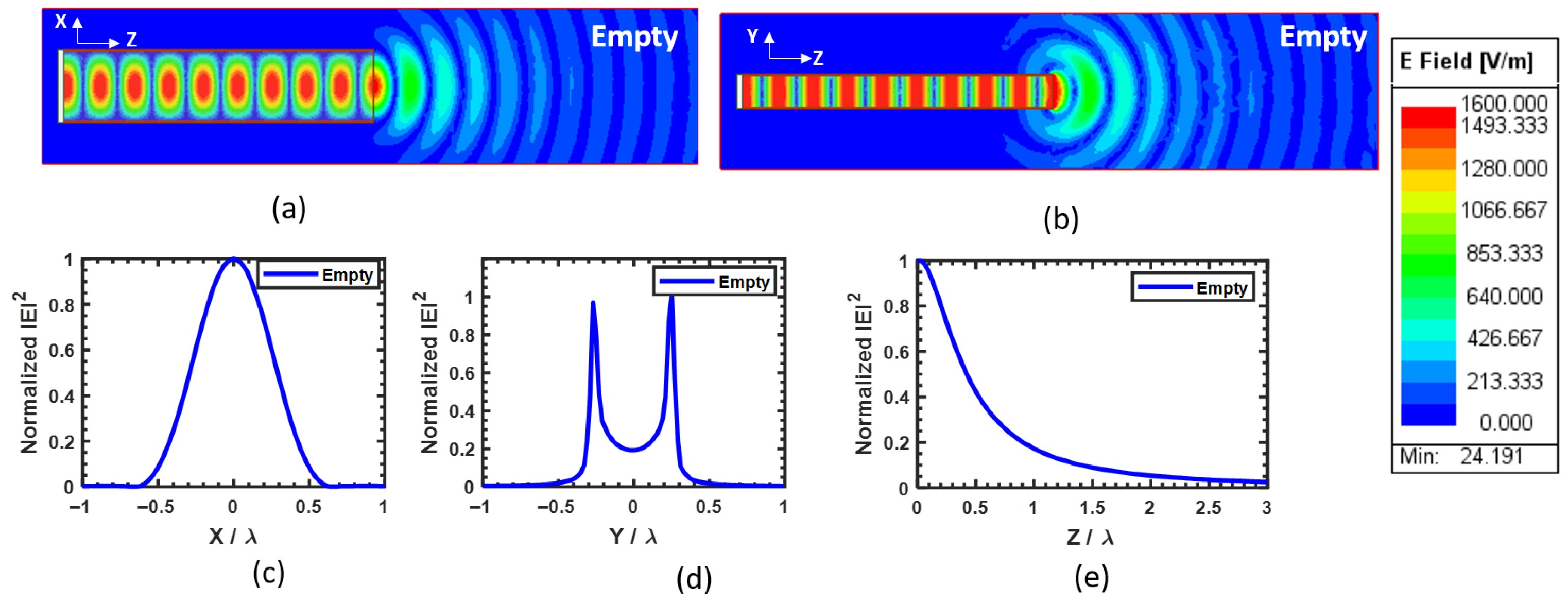
Rectangular probes, whether loaded with dielectric materials or left empty, produce local confinement of the electromagnetic field near their aperture. To illustrate this behavior, an open WR90 rectangular waveguide—operating in its single-mode frequency band from the 8.2 GHz to the 12.4 GHz frequency band—is excited in the fundamental TE10 mode. The simulation results are presented in Figure 3.
Analysis of Figure 3a,b reveals that the electric field is primarily confined within the waveguide. The portion of the field radiated into free space in the near-field region adopts a spherical shape immediately after exiting the waveguide. Figure 3c,d show the intensity profile extracted in air at the waveguide aperture ( z = 0 + ). A half-power beamwidth of 0.72 λ 0 is observed along the x-axis, while the electric field is mainly concentrated along the metallic surface of the waveguide in the y-direction. To assess the beam length, a longitudinal section starting from the aperture—shown in Figure 3e—demonstrates exponential decay of the electromagnetic field intensity. These observations are consistent with previously reported results in the literature [19,20].

3.1.2. Focusing the Electromagnetic Field Using an Electromagnetic Jet Lens

The rectangular waveguide is fully filled with PTFE, and a pyramidal transition is employed to ensure impedance matching. Subsequently, to tailor the electromagnetic field at the waveguide’s aperture and generate an electromagnetic jet, a PTFE jet lens is integrated at the output (Figure 1).
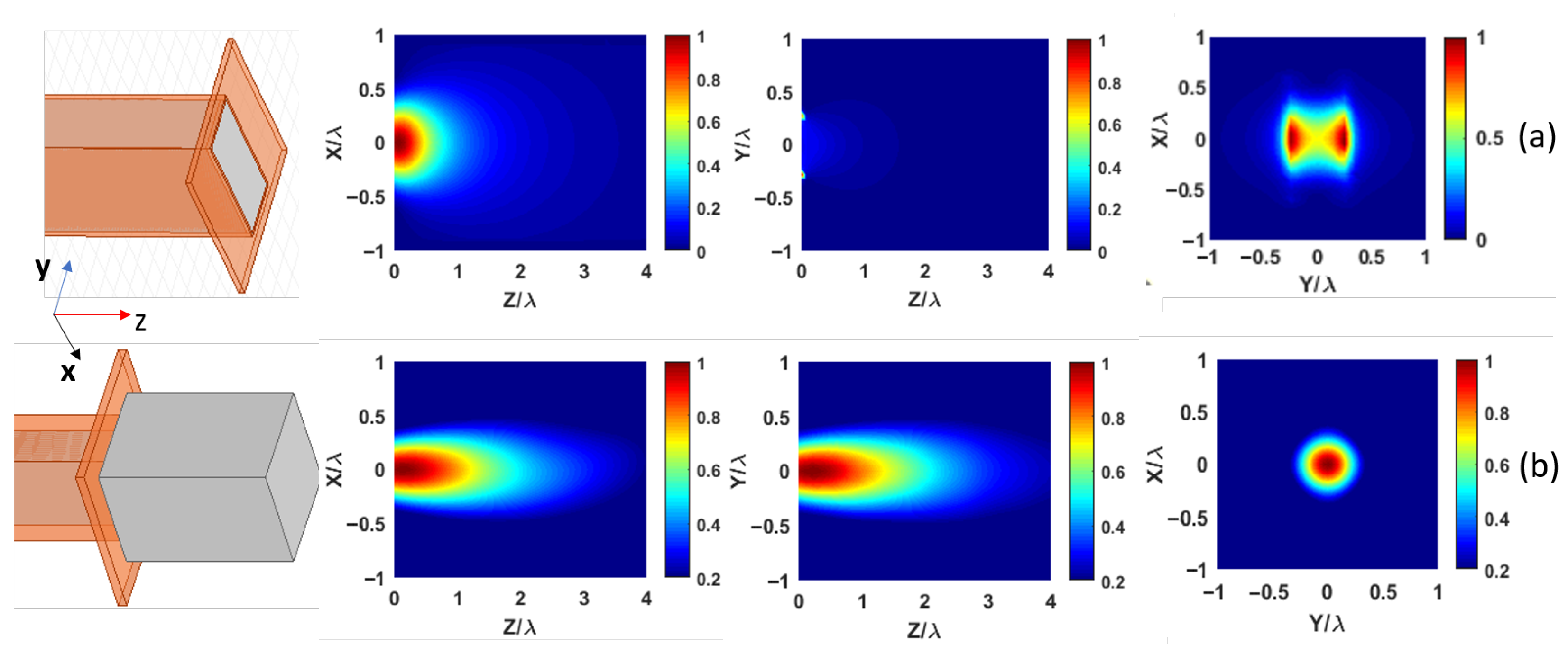
Figure 4a presents the electromagnetic field intensity concentration at the output of the waveguide equipped solely with the impedance-matching section, excluding the lens. The impedance matching and the dielectric loading do not induce any significant alteration in the field concentration at the aperture. As previously observed in Figure 3, the field concentration remains comparable to that of the unloaded waveguide.
Figure 4b illustrates the electromagnetic field profile for the configuration in which the impedance-matching section is followed by the electromagnetic jet lens. The origin z = 0 is defined at the lens exit. The integration of the jet lens enhances wave propagation along the z-axis, with the maximum field intensity occurring at a distance of 0.1λ from the lens (Figure 4b). Unlike the open-waveguide case, the electric field concentration is now similar in both the xz-plane and the yz-plane (Figure 4b), indicating the formation of a well-defined focal point.
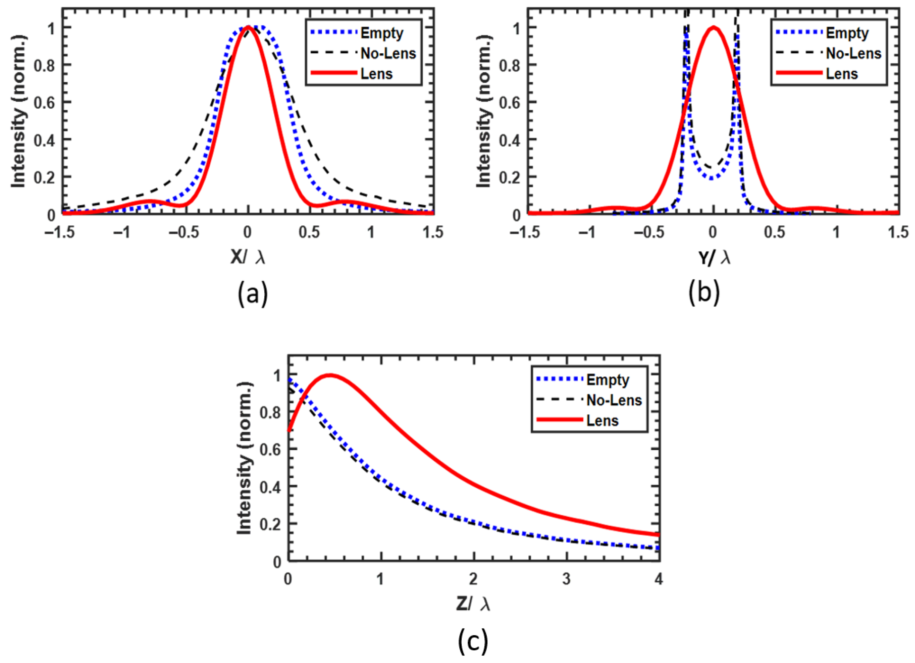
In addition to displacing the focal point outside the waveguide structure and enhancing the spatial confinement of the focused field, the lens also contributes to a reduction in the beam’s full width at half maximum (FWHM). Specifically, the FWHM decreases from 0.82λ to 0.59λ along the x-axis (Figure 5a), and it drops below the diffraction limit, reaching 0.41λ, along the y-axis (Figure 5b). Furthermore, along the z-axis, the lens significantly extends the longitudinal extent of the high-intensity region in the propagation direction, as shown in Figure 5c. This extended focal region is particularly advantageous for enabling subsequent contactless characterization or interaction with external samples positioned beyond the waveguide aperture.
Figure 6 illustrates the field propagation inside and outside the structures, at a frequency of 12 GHz. The configuration employing a dielectric-loaded waveguide with only the impedance-matching section is presented in Figure 6a. The resulting wavefronts in free space closely resemble those observed for the unloaded waveguide, with the notable exception that the maximum field intensity is no longer located exactly at the waveguide aperture but slightly displaced into the air. This shift indicates that the dielectric loading exerts a minor influence on the wave behavior at the waveguide’s exit.
In comparison, the integration of the electromagnetic jet lens leads to significant transformation of the wavefront shape. In addition to the emergence of a well-defined focal point outside the structure, a localized planar wavefront—characteristic of an electromagnetic jet—is clearly observed, accompanied by an amplitude enhancement exceeding 700 V/m in the electric field.
The analysis of the wavefront provides valuable insight into the underlying mechanism of electromagnetic jet formation. The PTFE extension placed at the end of the waveguide modifies the curvature of the wavefronts, transitioning from convex at the waveguide aperture to concave at the end of the electromagnetic jet lens. This transformation results from the difference in phase velocity between air and PTFE: the dielectric slows the propagation of the inner part of the wave, while the outer part propagates at the original speed. Upon exiting the lens, refraction in free space accentuates the curvature, forming a focused beam. At the focal distance, the initially concave wavefront gradually transitions back to a convex shape. In this region, the wave can be locally considered to be planar [21].

3.1.3. Impact of Frequency on the Electromagnetic Jet

At 12 GHz, the empty section of the waveguide on the source side operates in the single-mode regime. Consequently, although higher-order modes may be locally excited at discontinuities—such as the pyramidal transition, the waveguide aperture, or the lens–air interface—they cannot propagate efficiently in the empty section of the waveguide.
To investigate the influence of frequency variation on electromagnetic jet formation, the excitation frequency was increased to 15 GHz, corresponding to the Ku-band. At this frequency, up to three higher-order modes may be supported by the empty waveguide, potentially interfering with the overall wave propagation.
The normalized electric field intensities shown in Figure 7 reveal that the electromagnetic jet is fully emitted at the lens output, forming a beam that propagates over a distance of approximately 2λ before attenuation begins (see Figure 7a,b). This confirms that the dominant mode TE10 is well preserved, with no significant contribution from higher-order modes.
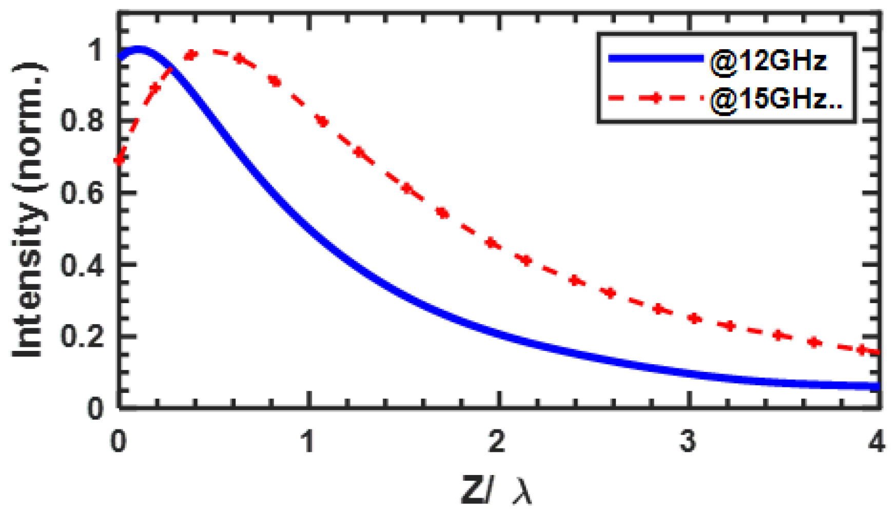
Moreover, although the phenomenon is observed at a different frequency, it exhibits similar characteristics to those observed at 12 GHz. The frequency increase slightly extends the beam length and shifts the location of the peak electric field intensity further from the lens output, as shown in Figure 8, while the beam width remains essentially unchanged.

3.1.4. Characteristics of the Electromagnetic Jet Lens

Figure 1b shows the electromagnetic jet lens, which can be directly inserted into a waveguide. The lens functionality is provided by the exterior part of the structure, which has been optimized based on its geometric parameters, notably the length ( L z ), width ( L x ), and height ( L y ). The material used for the lens is polytetrafluoroethylene (PTFE), which has a dielectric constant of 2.1 and very low losses.
The performance of the electromagnetic jet lens was evaluated by varying its geometric dimensions ( L z , L x , and L y ). Figure 9 illustrates the electric field concentration in the transverse plane, along the x and y-directions, for different configurations.
Figure 9a illustrates the effect of increasing the lens height L y . A larger L y extends the focal region, where the field exhibits a quasi-plane wave behavior, leading to pronounced beam elongation (up to FLHM = 3.1 λ ). At the same time, the focal point is pushed back to a distance of z = 1.2 λ from the waveguide aperture. Nonetheless, this configuration also yields a drop in the maximum field intensity, down to a normalized value of 0.68.
In Figure 9b, the influence of the lens width L x is analyzed. Increasing L x enhances the transverse symmetry of the beam, resulting in convergence of the beam widths in both directions ( FWHM x FWHM y ).
In Figure 9c, the transverse dimensions are set to equal values ( L x = L y ). Although the transverse dimensions are equal, the resulting field concentration remains non-symmetric, indicating that geometric symmetry does not guarantee a symmetric electromagnetic beam. Nevertheless, this non-symmetry leads to a beam length in the y-direction under the diffraction limit ( FWHM y = 0.44 λ ) accompanied by an increase in the maximum field intensity.
Figure 9d shows the impact of increasing the lens length L z . As L z grows, the focal point moves closer to the lens aperture ( Z max decreases); in addition, the peak field intensity approaches its maximum (normalized value 1 ), but the beam length (FLHM) shortens. Notably, the beam width in the y-direction reaches an optimal value of FWHM y = 0.39 λ , representing the best focusing performance achieved in the X-band to date. This performance also compares favorably with that achieved in previous reports: FWHM 0.49 λ for a dielectric sphere at 0.81 THz [22]; FWHM 0.5 λ at 30 GHz in a parallel-plate waveguide [13]; and FWHM 0.33 λ at 0.1 THz in a circular waveguide with metamaterial [23]. However, in the latter case the FLHM was limited to only λ . These results highlight the very good near-field focusing capability of the proposed jet lens design.
The results of this study are summarized in Table 1, which presents the effects of varying the lens dimensions on the focal point position, the maximum electric field intensity, and the beam width and length.
The results summarized in Table 1 indicate that when the focal point ( Z max ) is positioned closer to the lens surface, the maximum normalized intensity attains its peak value, while both the full width at half maximum along the y-axis (FWHMy) and the beam length (FLHM) are minimized. Conversely, as Z max shifts further from the lens, the maximum intensity decreases, accompanied by an increase in the FWHM and an extended beam length.
These results provide valuable guidelines for the design and optimization of dielectric jet lenses, enabling the tailoring of focal length, beam confinement, and intensity depending on application-specific constraints such as spatial resolution, working distance, or sensitivity requirements.

3.2. Experimental Validation of Electromagnetic Jet Mapping

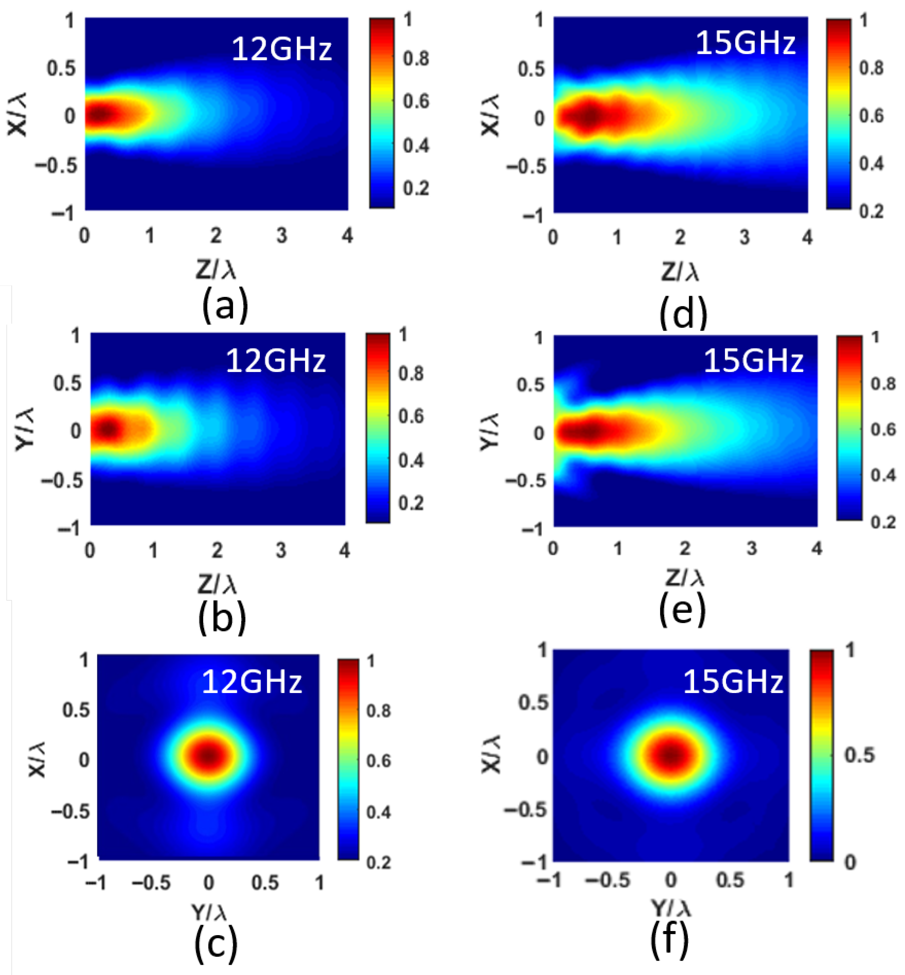
Lens 3 was fabricated instead of Lens 4 in order to ensure that the focal point is located outside the lens. Figure 10 shows the experimental mapping of the electromagnetic field intensity at the lens output at 12 GHz and 15 GHz , measured in the x z plane (Figure 10a), the y z plane (Figure 10b), and the x y plane (Figure 10c). As observed, the measurements are in very good agreement with the numerical simulations: a clear focusing effect is achieved, well beyond the lens aperture. The focal spot is seen to shift with increasing frequency, as predicted.
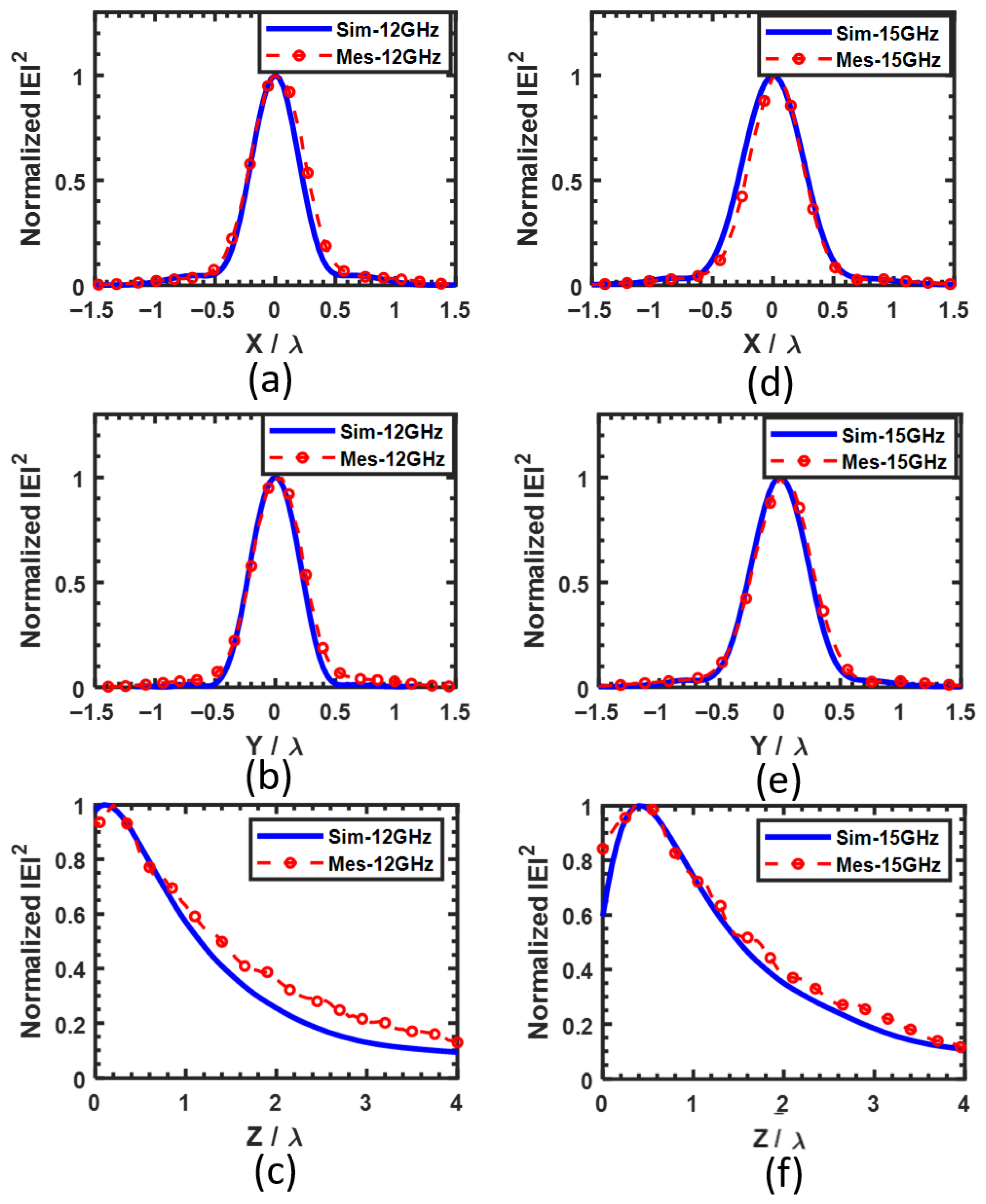
Some oscillations are nevertheless visible in the measured field maps. After laboratory testing and analysis, these oscillations were attributed to standing waves generated by the metallic parts of the measurement probe. This interpretation is further confirmed by the profiles in Figure 11c,f, which exhibit no such perturbations, thus ruling out the excitation of higher-order modes. A possible solution to mitigate this effect would be to employ a second lens inserted into the probe waveguide, thereby displacing the metallic parts further away and limiting standing-wave formation. Nevertheless, this phenomenon has only a minor influence on the overall field distribution and does not compromise the validity of the results.
The normalized intensity profiles ( | E | 2 ) at both frequencies are compared with numerical simulations along a line passing through the focal point, as shown in Figure 11a–f. Excellent agreement is observed between the experimental measurements and simulations. In particular, the full width at half maximum along the y-axis is found to be well below the diffraction limit ( FWHM y = 0.46 λ ), as predicted by the simulations.
This close correspondence confirms the ability of the proposed lens design to generate an electromagnetic jet at the output aperture of the rectangular waveguide. The observed focusing properties—namely the sub-diffraction beam confinement and the extended propagation of a quasi-collimated field—provide clear experimental evidence of electromagnetic jet formation in this guided-wave configuration.

4. Conclusions

In this work, we have demonstrated the innovative integration of a dielectric jet lens directly at the aperture of a rectangular waveguide, achieved here for the first time in the X- and Ku-bands. The lens design, including the pyramidal transition, effectively minimizes discontinuity losses while preserving the dominance of the fundamental TE10 mode. The numerical simulations and experimental measurements show excellent agreement.
Compared to conventional open-ended waveguides, the proposed PTFE lens enables near-field focusing at a certain distance from the structure’s end, forming a narrow beam that propagates over several wavelengths before attenuation.
By systematically varying the lens dimensions (Lx, Ly, and Lz), we have demonstrated precise control over the focal region, beam elongation, and peak intensity. Optimal focusing performance was achieved with a beam width of FWHMy = 0.39λ, indicating superior near-field concentration relative to previous free-space and guided-wave configurations. Furthermore, increasing the excitation frequency from 12 GHz to 15 GHz allows the focal point to shift significantly beyond the lens.
These results confirm the generation of an electromagnetic jet with distinct properties. In particular, the experimental measurements validate sub-diffraction focusing, with a beam width of FWHMy = 0.44λ, in excellent agreement with the simulations.
The proposed guided-structure approach offers a versatile platform for applications including detection, imaging, and local field characterization. Given the X- and Ku-band operation, this solution is particularly promising for probing opaque or highly lossy materials.

Author Contributions

Conceptualization, A.D. and B.S.; methodology, A.D.; validation, B.S. and M.P.A.; software, B.B.; investigation, A.D., M.G. and B.S.; resources, B.B.; Validation, B.S.; visualization, A.D.; writing—original draft preparation, A.D. and M.G.; writing—review and editing, B.S.; Supervision, B.S.; project administration, B.S. All authors have read and agreed to the published version of the manuscript.

Funding

We would like to thank the French Development Agency for providing financial support to the PEA-Chad project.

Conflicts of Interest

The authors declare no conflicts of interest.

Abbreviations

The following abbreviations are used in this manuscript:
FWHMxFull width at half maximum along the x-axis
FWHMyFull width at half maximum along the y-axis
FLHMFull length at half maximum along the z-axis
PTFEPolytetrafluoroethylene
TRLThru/Reflect/Line calibration method

References

  1. Gardiol, F. Open-ended waveguides: Principles and applications. Adv. Electron. Electron Phys. 1985, 63, 139–187. [Google Scholar]
  2. Baudrand, H.; Tao, J.-W.; Atechian, J. Study of radiating properties of open-ended rectangular waveguides. IEEE Trans. Antennas Propag. 2002, 36, 1071–1077. [Google Scholar] [CrossRef]
  3. Tantot, O.; Chatard-Moulin, M.; Guillon, P. Measurement of complex permittivity and permeability and thickness of multilayered medium by an open-ended waveguide method. IEEE Trans. Instrum. Meas. 2002, 46, 519–522. [Google Scholar] [CrossRef]
  4. Ramzi, M.R.; Abou-Khousa, M.; Prayudi, I. Near-field microwave imaging using open-ended circular waveguide probes. IEEE Sens. J. 2017, 17, 2359–2366. [Google Scholar] [CrossRef]
  5. Ur Rahman, M.S.U.; Gaya, S.M.; Abou-Khousa, M.A. Nondestructive testing and evaluation of surface cracks using a planar microwave resonator probe. In Proceedings of the 2022 IEEE Microwaves, Antennas, and Propagation Conference (MAPCON), Bangalore, India, 12–16 December 2022; pp. 552–556. [Google Scholar]
  6. Ur Rahman, M.S.; Mustapha, A.A.; Abou-Khousa, M.A. Detection and sizing of surface cracks in metals using a UHF probe. In Proceedings of the 2021 IEEE International Conference on Imaging Systems and Techniques (IST), Kaohsiung, Taiwan, 24–26 August 2021; pp. 1–5. [Google Scholar]
  7. Huber, C.; Abiri, H.; Ganchev, S.I.; Zoughi, R. Modeling of surface hairline-crack detection in metals under coatings using an open-ended rectangular waveguide. IEEE Trans. Microw. Theory Tech. 2002, 45, 2049–2057. [Google Scholar] [CrossRef]
  8. Mbarek, S.B.; Choubani, F.; Cretin, B. Study of a new micromachined coplanar probe for near-field microwave microscopy. Microsyst. Technol. 2018, 24, 2887–2893. [Google Scholar] [CrossRef]
  9. Varshney, P.K.; Akhtar, M.J. Near-field subsurface microwave imaging using a planar sensor based on substrate-integrated waveguide. In Proceedings of the 2018 IEEE MTT-S International Microwave and RF Conference (IMaRC), Kolkata, India, 28–30 November 2018; pp. 1–4. [Google Scholar]
  10. Héritier, M.; Pachlatko, R.; Tao, Y.; Abendroth, J.M.; Degen, C.L.; Eichler, A. Spatially resolved surface dissipation over metal and dielectric substrates. Phys. Rev. Lett. 2021, 127, 216101. [Google Scholar] [CrossRef] [PubMed]
  11. Chen, Z.; Taflove, A.; Backman, V. Photonic nanojet enhancement of backscattering of light by nanoparticles: A potential novel visible-light ultramicroscopy technique. Opt. Express 2004, 12, 1214–1220. [Google Scholar] [CrossRef] [PubMed]
  12. Lecler, S.; Takakura, Y.; Meyrueis, P. Properties of a three-dimensional photonic jet. Opt. Lett. 2005, 30, 2641–2643. [Google Scholar] [CrossRef] [PubMed]
  13. Ounnas, B.; Sauviac, B.; Takakura, Y.; Lecler, S.; Bayard, B.; Robert, S. Single and Dual Photonic Jets and Corresponding Backscattering Enhancement with Tipped Waveguides: Direct Observation at Microwave Frequencies. IEEE Trans. Antennas Propag. 2015, 63, 5612–5618. [Google Scholar] [CrossRef]
  14. Hyani, H.; Sauviac, B.; Edee, K.; Granet, G.; Robert, S.; Bayard, B. Multi-waveguide tip for photonic jet generation applied to detection in opaque structures. In Proceedings of the 15th Edition of the Microwave and Materials Characterization Days (JCMM), Paris, France, 19–21 March 2018. [Google Scholar]
  15. Johnson, S.G.; Bienstman, P.; Skorobogatiy, M.A.; Ibanescu, M.; Lidorikis, E.; Joannopoulos, J.D. Adiabatic theorem and continuous coupled-mode theory for efficient taper transitions in photonic crystals. Phys. Rev. E 2002, 66, 066608. [Google Scholar] [CrossRef] [PubMed]
  16. Wei-Ping, H. Coupled-mode theory for optical waveguides: An overview. J. Opt. Soc. Am. A 1994, 11, 963–983. [Google Scholar] [CrossRef]
  17. Hyani, H.; Sauviac, B.; Edee, M.K.; Granet, G.; Robert, S. Numerical study of a photonic jet with aperiodic Fourier modal method and experimental validation. Prog. Electromagn. Res. C 2018, 88, 133–143. [Google Scholar] [CrossRef]
  18. Engen, G.F.; Hoer, C.A. Thru-reflect-line: An improved technique for calibrating the dual six-port automatic network analyzer. IEEE Trans. Microw. Theory Tech. 1979, 27, 987–993. [Google Scholar] [CrossRef]
  19. Baskakova, A.; Hoffmann, K. Investigation of waveguide sensors for ultra-short-distance measurements. In Proceedings of the 2019 93rd ARFTG Microwave Measurement Conference (ARFTG), Boston, MA, USA, 7 June 2019; pp. 1–4. [Google Scholar] [CrossRef]
  20. Baskakova, A.; Hoffmann, K. W-Band imaging sensor using a rectangular waveguide structure with choke. IEEE Microw. Wirel. Components Lett. 2021, 32, 230–233. [Google Scholar] [CrossRef]
  21. Granger, M.; Ghaddar, A.; Bayard, B.; Sauviac, B. Towards a local free-space microwave characterization method. In Proceedings of the 2024 IEEE/MTTS International Microwave Symposium (IMS), Washington, DC, USA, 16–21 June 2024; pp. 912–915. [Google Scholar] [CrossRef]
  22. Wei, B.; Chen, R.; Xu, Q.; Li, R.; Gong, S.; Yan, S. Optical force on a Rayleigh particle generated by photonic jet. Opt. Rev. 2024, 31, 41–53. [Google Scholar] [CrossRef]
  23. Li, X.; Wang, Z.; Jiang, H.; Deng, M.; Yin, L.; Gong, C.; Liu, W. Super-resolution terahertz imaging based on a meta-waveguide. Opt. Lett. 2024, 49, 1261–1264. [Google Scholar] [CrossRef]
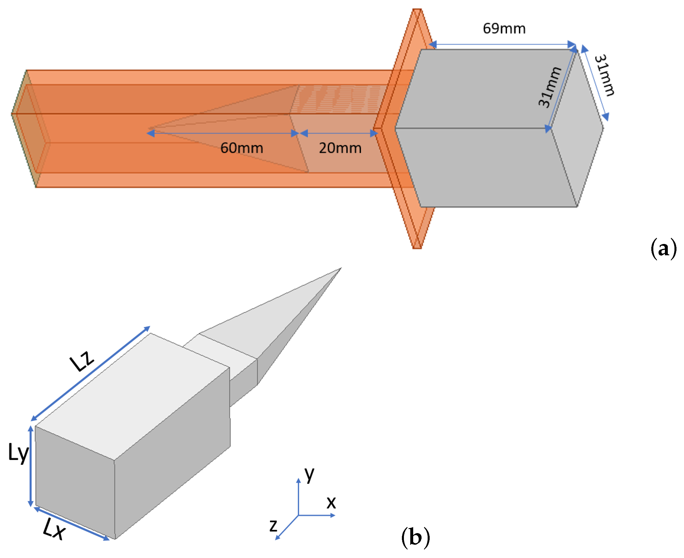
Figure 1. Structure under study. (a) Rectangular metallic WR90 waveguide (translucent orange) with inserted PTFE dielectric lens (gray). Complete device forming electromagnetic jet lens: from left to right, pyramidal impedance-matching section inside waveguide, dielectric section fully filling waveguide, and parallelepiped termination outside waveguide. (b) PTFE dielectric lens.
Photonics 12 00895 g001
Figure 2. Schematic of the experimental setup.
Photonics 12 00895 g002
Figure 3. Modeling of the near-field distribution at 12 GHz for an open, unloaded rectangular waveguide. Visualization of the real part of the electric field mapped in the x z -plane (a) and in the y z -plane (b). Field intensity profile extracted at the aperture ( z = 0 ) along the x-axis (c), along the y-axis (d), and along the propagation axis (z-axis) starting from z = 0 (e).
Photonics 12 00895 g003
Figure 4. Modeling of electric field intensity at 12 GHz for an open waveguide (a) with impedance matching (part 1) and (b) with the addition of the electromagnetic jet lens. The field mappings in the right-hand column are presented at the z-plane corresponding to the maximum field intensity.
Photonics 12 00895 g004
Figure 5. Comparison of the electromagnetic field intensity at the output of the empty guide (solid line), the dielectric-loaded waveguide without the lens (dotted line), and the waveguide with an electromagnetic lens (dashed line) along the x-axis (a), the y-axis (b), and the z-axis (c).
Photonics 12 00895 g005
Figure 6. Numerical simulation of the real part of the electromagnetic field at 12 GHz for an open dielectric-loaded waveguide with only the impedance matching part (a) and with the complete electromagnetic jet lens (b).
Photonics 12 00895 g006
Figure 7. Normalized field intensity concentration of a waveguide terminated with a PTFE electromagnetic jet lens simulated at 15 GHz (a) in the x-z plane, (b) in the y-z plane, and (c) in the x-y plane.
Photonics 12 00895 g007
Figure 8. Longitudinal profile of the normalized intensity ( | E | 2 ) extracted from the field map for 12 GHz and 15 GHz , starting from z = 0 .
Photonics 12 00895 g008
Figure 9. Normalized electric field intensity distributions in free space along the x- and y-axes, simulated at 15 GHz , for different geometrical configurations of the electromagnetic jet lens: (a) configuration with L y > L x ; (b) configuration with L y < L x ; (c) configuration with L y = L x ; (d) configuration with L y = L x and increased L z .
Photonics 12 00895 g009
Figure 10. Experimental measurement of normalized intensity at the output of the PTFE lens: (a) x z plane, (b) y z plane, and (c) x y plane at 12 GHz; (d) x z plane, (e) y z plane, and (f) x y plane at 15 GHz.
Photonics 12 00895 g010
Figure 11. Normalized intensity profiles ( | E | 2 ) along a line passing through the focal point. Profiles at 12 GHz are shown in (a) along the x-axis, (b) along the y-axis, and (c) along the z-axis; profiles at 15 GHz are shown in (d) along the x-axis, (e) along the y-axis, and (f) along the z-axis. The experimental measurements (markers) are compared with the numerical simulations (solid lines), showing very good agreement.
Photonics 12 00895 g011
Table 1. Parametric study of the lens at 15 GHz : length ( L z ), width ( L x ), and height ( L y ). The bold and italic fonts highlight the optimal values for the various characteristics of the electromagnetic jet across the different configurations.
FWHMxFWHMyFLHM Z max Normalized | E | 2
Lens 1—Figure 9a: L z = 69   mm , L x = 31   mm , L y = 35   mm
0.52 λ 0.67 λ 3.1 λ 1.2 λ 0.68
Lens 2—Figure 9b: L z = 69   mm , L x = 35   mm , L y = 31   mm
0.60 λ 0.61 λ 2.0 λ 0.8 λ 0.72
Lens 3—Figure 9c: L z = 69   mm , L x = 31   mm , L y = 31   mm
0.59 λ 0.44 λ 1.8 λ 0.6 λ 0.95
Lens 4—Figure 9d: L z = 72   mm , L x = 31   mm , L y = 31   mm
0.59 λ 0.39 λ 1.5 λ 0.4 λ 1
Disclaimer/Publisher’s Note: The statements, opinions and data contained in all publications are solely those of the individual author(s) and contributor(s) and not of MDPI and/or the editor(s). MDPI and/or the editor(s) disclaim responsibility for any injury to people or property resulting from any ideas, methods, instructions or products referred to in the content.