Article

Optimal Design of a Lightweight Terahertz Absorber Featuring Ultra-Wideband Polarization-Insensitive Characteristics

1
State Key Laboratory of Extreme Environment Optoelectronic Dynamic Measurement Technology and Instrument, North University of China, Taiyuan 030051, China
2
Opto-Electronics Information Technology, Ministry of Education, School of Precision Instruments and Opto-Electronics Engineering, Tianjin University, Tianjin 300072, China
*
Authors to whom correspondence should be addressed.
Photonics 2025, 12(8), 787; https://doi.org/10.3390/photonics12080787 (registering DOI)
Submission received: 26 June 2025 / Revised: 25 July 2025 / Accepted: 30 July 2025 / Published: 4 August 2025
(This article belongs to the Special Issue Metamaterials and Nanophotonics: Fundamentals and Applications)

Abstract

Metamaterial absorbers in terahertz (THz) based bands have garnered significant attention for their potential applications in military stealth, terahertz imaging, and other fields. Nevertheless, the limited bandwidth, low absorption rate, and heavy weight greatly reduce the further development and wide application of terahertz absorbers. To solve these problems, we propose a polystyrene (PS)-based ultra-broadband metamaterial absorber integrated with a polyethylene terephthalate (PET) double-sided adhesive layer and a patterned indium tin oxide (ITO) film through the simulation method, which operates in the THz band. The electromagnetic wave absorption properties and underlying physical absorption mechanisms of the proposed metamaterial absorbers are comprehensively modeled and rigorously numerically simulated. The research demonstrates the metamaterial absorber can achieve absorption performance of over 90% for fully polarized incident waves in the ultra-wideband range of 1.2–10 THz, especially achieving perfect absorption characteristics of over 99.9% near 1.8–1.9 THz and 5.8–6.2 THz. The proposed absorber has a lightweight physical property of 0.7 kg/m2 and polarization-insensitive characteristic, and it achieves a broad-angle that allows a range of incidence angles up to 60°. The simulation research results of this article provide theoretical support for the design of terahertz absorbers with ultra-wideband absorption characteristics.

1. Introduction

Terahertz (THz) waves are typically defined as electromagnetic waves with frequencies in the range of 0.1–10 THz, corresponding to wavelengths in the range of 30–3000 μm [1,2]. With the rapid advancement of THz radar technology [3], security risks such as information leakage, electromagnetic interference, and target exposure have become increasingly prominent in the military domain. Therefore, the development of THz stealth and electromagnetic wave-absorbing technology [4] is of great significance for enhancing battlefield survivability and the level of military modernization. Stealth materials, which are an important part of stealth technology applications, are a key area of research and development in global weapon and equipment systems. However, the stealth performance of traditional stealth materials cannot meet the requirements of the THz band [5]. Consequently, there is an urgent need to achieve greater breakthroughs in THz band stealth technology, which has the characteristics of lightweight, polarization insensitive, and wideband stealth effects.
Metamaterial absorbers are entities that can efficiently absorb incident electromagnetic waves or significantly reduce their energy [6]. They employ various loss mechanisms to convert electromagnetic waves into thermal energy or other forms and then gradually dissipate the converted energy, ultimately achieving the effects of absorption and stealth. Metamaterials can have a target operating frequency and range of action that span the entire spectral band [7]. In theory, functional metamaterials suitable for different wavelengths can be designed [8], and the scale and morphology of their structural characteristic units are determined by the working wavelength [9]. Unique functions such as negative refraction [10], invisibility cloak [11], polarization multiplexed metasurface [12], surface plasmon resonance [13], and perfect absorption [14,15,16,17,18,19] are all achieved through the rational design of metamaterials. The successful preparation of metamaterial perfect absorbers and their application in the field of stealth provide new insights for the subsequent research on THz absorption and stealth technology. In 2018, Meng et al. proposed a polarization-insensitive THz perfect metamaterial absorber [20], which has five distinct absorption bands with an average absorption peak greater than 99%. In 2020, Wang et al. advanced a tunable THz absorber based on black phosphorus (BP), which achieved broadband THz wave absorption of 8% to 98% in the 2–10 THz band [21]. On this basis, researchers presented various design schemes to improve the absorption performance of metamaterials at large incident angles [7,19,22,23,24]. However, the existing design of absorbing materials makes it difficult to balance the all-round absorption characteristics of high absorption efficiency, large bandwidth, full polarization response, lightweight, flat structure, and simple structure [25], greatly limiting their practical applications. With the rapid development of micro–nano fabrication technology, the preparation of multi-layer metamaterials has become possible. This material can be designed in three-dimensional space, with greater control space and design freedom.
This article proposes an ultra-wideband THz planar absorber, and simulation results show that it exhibits an absorption performance exceeding 90% in the range of 1.2–10 THz, and this absorber has a simple and stable structure. Due to the lightweight and thin characteristics of PS foam, PET, and ITO materials, the whole absorber structure is ultra-lightweight, with an estimated unit weight of only 0.7 kg/m2, which is about one percent of the mass of conventional absorbers with the same size at present [26,27]. This simulation design work has important reference value for the development of efficient, ultra-wideband, fully polarized, and ultra-light absorbing metamaterials.

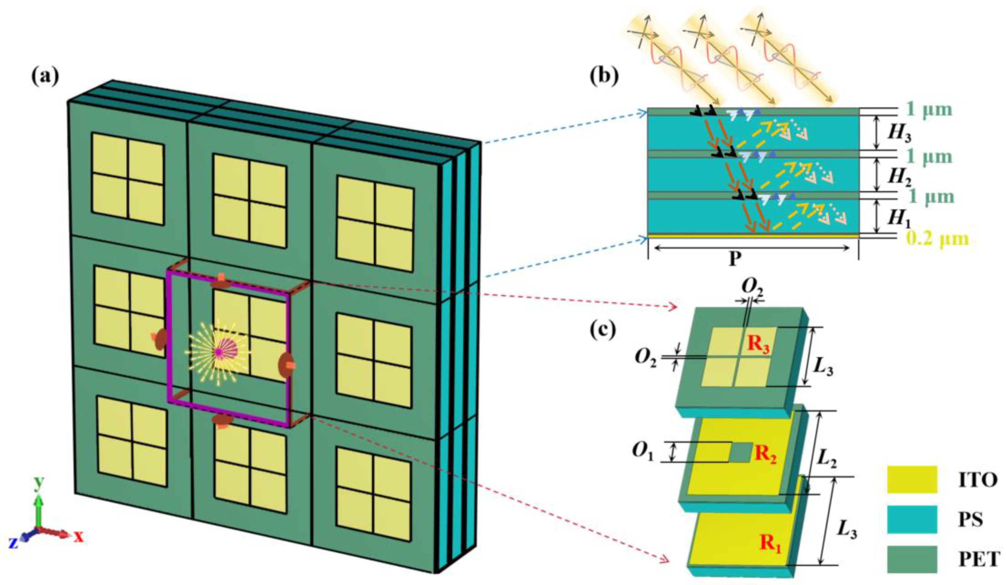
2. Materials and Methods

A schematic of the metamaterial absorber designed in this paper, featuring a meticulously structured unit cell for efficient electromagnetic wave absorption, is presented in Figure 1a. The unit array is square, and the side length of the substrate foam is P. As illustrated in Figure 1b,c, the unit structure comprises three distinct layers of PS foam, each serving as a dielectric-absorbing layer. We define the plane of terahertz wave incidence shown in Figure 1b as the terahertz wave incidence surface. An ITO structure is seamlessly integrated onto each PS layer using a PET (1 μm) double-sided adhesive, ensuring robust mechanical connections. The dielectric constant of the PET layer is 2.62, and the loss tangent is 0.014 [28]. At the bottom of the unit cell lies a metalloid-like ITO layer with a sheet resistance of 5 Ω. The PS foam in each isolation layer exhibits a dielectric constant of 1.1 and a loss tangent of 0.018 and the almost non-existent dispersion of PS materials within the terahertz band [29]. Their thicknesses are denoted as H1, H2, and H3, respectively, with these parameters playing a crucial role in tailoring the absorber’s electromagnetic response. The first-layer ITO structure is configured as a square patch, featuring a side length of L1 and a sheet resistance of R1. In the middle layer, an ITO square ring is incorporated, where the outer ring has a width of L2, and the inner ring has a width of O1, along with a sheet resistance of R2. As for the top-layer unit structure, it comprises a foam layer with a thickness of H3, within which four small square ITO patches of identical dimensions are embedded. Each of these patches has a side length of L3 and a sheet resistance of R3. The parameter-optimized dimensions of the unit cell in Figure 1 are P = 50 μm, H1 = H2 = H3 = 9 μm, O1 = 10 μm, O2 = 1 μm, L1 = 48 μm, L2 = 43 μm, L3 = 30 μm, and R1 = R2 = R3 = 200 Ω/sq.
The absorption rate of the absorber can be calculated using Formula (1).
A ( ω ) = 1 R ( ω ) T ( ω ) = 1 | S 11 | 2 | S 21 | 2
where R and S11 represent the reflection and the reflection S parameter, respectively, and T and S21 represent the transmission and the transmission S parameter, respectively. Owing to the inherent metallic characteristics of ITO, the absorber exhibits a transmittance that approaches zero. Under such circumstances, the absorption efficiency of the absorber is exclusively correlated with the reflection coefficient. Therefore, the absorption efficiency is simplified as Formulas (2) and (3).
A ω = 1 R ( ω ) = 1 S 11 2
A ( ω ) = 2 η 0 Re ( Z e f f ) + Im g ( Z e f f ) + η 0

3. Results

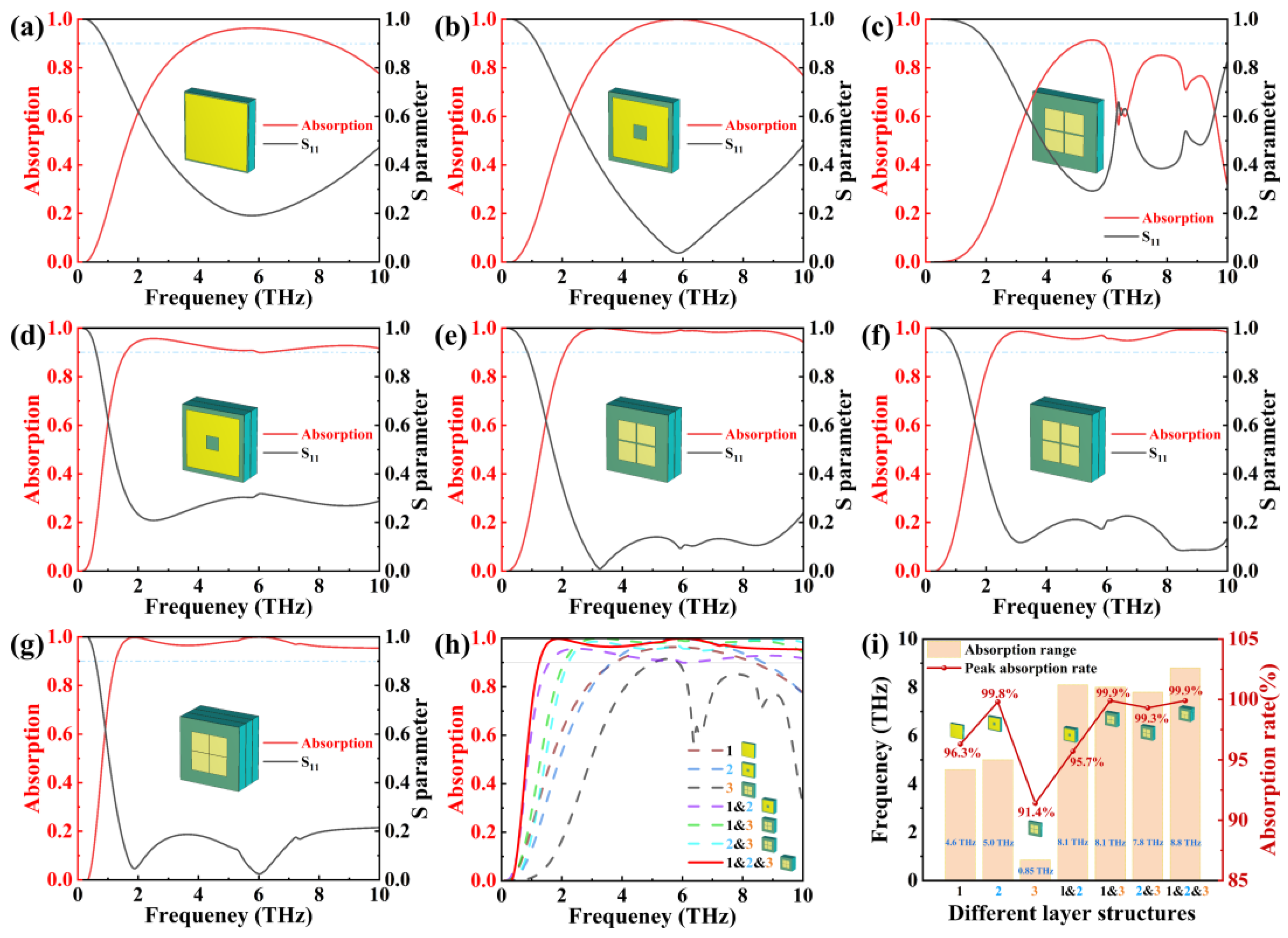
3.1. Result Analysis

To elucidate the operational mechanism of the proposed absorber, we conducted simulations of the absorber’s performance across varying layer configurations. Figure 2 presents a simulation of the absorption performance for the single-layer structure and the stacked multi-layer structure within this design framework. As illustrated in Figure 2a–c, the single-layer structure demonstrates inadequate absorption capability. In contrast, Structure 1 and Structure 2 exhibit an absorption capability exceeding 90% across a bandwidth of approximately 5 THz.
However, structure 3 only attains effective absorption within a narrow frequency range of 0.85 THz. The absorption performance is markedly improved following the stacking of a double-layer structure; however, the absorption bandwidth remains comparatively narrow. As illustrated in Figure 2d, the absorber comprising Structure 1 and Structure 2 exhibits absorption efficiencies exceeding 90% within the frequency ranges of 1.6–5.9 THz and 6.2–10 THz, yet its peak absorption rate is merely 95.7%. Figure 2e presents the simulation results for the absorber composed of Structure 1 and Structure 3. This absorber can attain a peak absorption rate as high as 99.9%, but it has a relatively narrow absorption bandwidth, achieving effective absorption only in the 2–10 THz band. Figure 2f displays the simulation outcomes of the absorber formed by Structure 2 and Structure 3. The device achieves an absorption rate greater than 90% across the frequency span of 2.2–10 THz, with a peak absorption rate of 99.3%. To broaden the effective absorption bandwidth and enhance the peak absorption rate, a simulation of a three-layer structure was carried out, as depicted in Figure 2g. This structure achieved stable broadband absorption (with a bandwidth of 8.8 THz) within the frequency range of 1.2–10 THz, and its peak absorption rate could reach 99.9%. Consequently, by comparing the simulation results of different structures presented in Figure 2h–i, it is evident that the absorber proposed in this study effectively broadens the absorption bandwidth and enhances the absorption efficiency, thereby exhibiting ultra-wideband and highly efficient absorption performance. Moreover, the simulation outcomes indicate that the proposed absorber attains perfect absorption of THz waves within the frequency ranges of 1.8–1.9 THz and 5.8–6.2 THz, featuring a peak absorption rate of 99.9%. This excellent absorption characteristic is due to the multiple interference reflections of terahertz waves in a three-layer structure.
According to the transmission line theory, we will quantitatively analyze the classical metal dielectric metal physical structure of metamaterial absorbers as an equivalent circuit containing parameters. Figure 3a illustrates the equivalent circuit model of the unit cell. In our unit cell, the three-layer structure composed of PS and PET acts as capacitors, while the inter-patch gaps or loops within the ITO patches can also be regarded as capacitors. The incorporation of an equivalent resistance based on the ITO resistance loss layer facilitates the effective dissipation of the incident electromagnetic wave. Each layer of the structure corresponds to a parallel RLC circuit. Given that the dielectric constant of foam is approximately equal to that of air, each foam layer can be considered as having the characteristic impedance of air, denoted as Z0. The dielectric medium within each layer is equivalent to a series-connected transmission line. The input impedance at various positions is correlated with the layer thickness. By matching the impedance of the structure with the air impedance to achieve Zin ≈ 377 Ω [30], optimal absorption performance can be attained. The transmission matrices of the top resonant structure, middle dielectric layer, and bottom metal substrate of metamaterials can be represented as follows [31,32]:
A u p B u p C u p D u p = 1 0 1 X 1 X 2 X 1 + X 2 + M 1
A middle B middle C middle D middle = cos ( k l ) j Z c Sin ( k l ) j Sin ( k l ) Z c cos ( k l )
A bottom B bottom C bottom D bottom = 1 0 1 X 3 1
where M represents the coupling between resonances; k is the wave vector of TEM waves; and l and Zc are the thickness and characteristic impedance of the intermediate dielectric layer, respectively.
So, the transmission matrix of metamaterial absorbers can be expressed as:
A B C D = A u p B u p C u p D u p A middle B middle C middle D middle A bottom B bottom C bottom D bottom = cos ( k l ) + j Z c Sin ( k l ) X 3 j Z c Sin ( k l ) 1 X 1 X 2 X 1 + X 2 + M cos ( k l ) + j Z c Sin ( k l ) X 3 Z c X 3 + Z c 2 X 1 X 2 X 1 + X 2 + M cos ( k l ) + j Z c Sin ( k l ) X 1 X 2 X 1 + X 2 + M
By combining impedance matching theory, effective medium theory, and transmission line theory, we can optimize the parameters of the metasurface structure to match its equivalent impedance with its own spatial wave impedance, thereby achieving broadband efficient absorption in the ideal frequency band. Therefore, the S parameters of metamaterials are:
S 11 S 12 S 21 S 22 = A Z 0 + B - ( C Z 0 + D ) Z i A Z 0 + B + ( C Z 0 + D ) Z i 2 Z i Z 0 A Z 0 + B - ( C Z 0 + D ) Z i 2 Z i Z 0 A Z 0 + B - ( C Z 0 + D ) Z i - A Z 0 + B - ( C Z 0 - D ) Z i A Z 0 + B - ( C Z 0 + D ) Z i
Ulteriorly, the parameters representing reflection, such as S11, were fitted and converted. The reflection loss of the circuit model is simulated, and the results are compared with those obtained from the electromagnetic model (Figure 3b). Consequently, three parallel-series circuits constitute the equivalent circuit of the ultra-wideband terahertz planar absorber proposed in this paper. Specifically, R11, L11, C11 represent the equivalent circuit of the bottom layer, while R22, L22, C22 and R33, L33, C33 correspond to the other two layers. We extracted parameter values from the RLC equivalent circuit using the Advanced Design System (Table 1). The ITO reflective layer with metallic properties at the bottom can be regarded as a short circuit [33]. The positions of the two resonance points in the simulation results are consistent with their actual locations. Given that the absorber devised in this study features a flexible base, a material bending simulation has been incorporated into the research. As illustrated in Figure 3c, the absorber sustains high-efficiency absorption even when subjected to bending angles of up to 45 degrees. Here, ‘a’ and ‘b’ denote the central angles corresponding to the upward and downward bending of the metamaterial, respectively. In addition, this study further conducted simulations to explore the effects of applying bias voltage and bias current (as depicted in Figure 3d). The simulation outcomes reveal that modulating the bias voltage enables precise control over the absorber’s switching behavior. However, it is noteworthy that an elevation in the bias voltage leads to a substantial decline in the absorption efficiency. However, the simulation results also indicate that augmenting the bias current induces only a marginal alteration in the absorption range of the material. Consequently, in subsequent research focused on tunability, the strategy of elevating the bias voltage will be employed to achieve the desired adjustments.

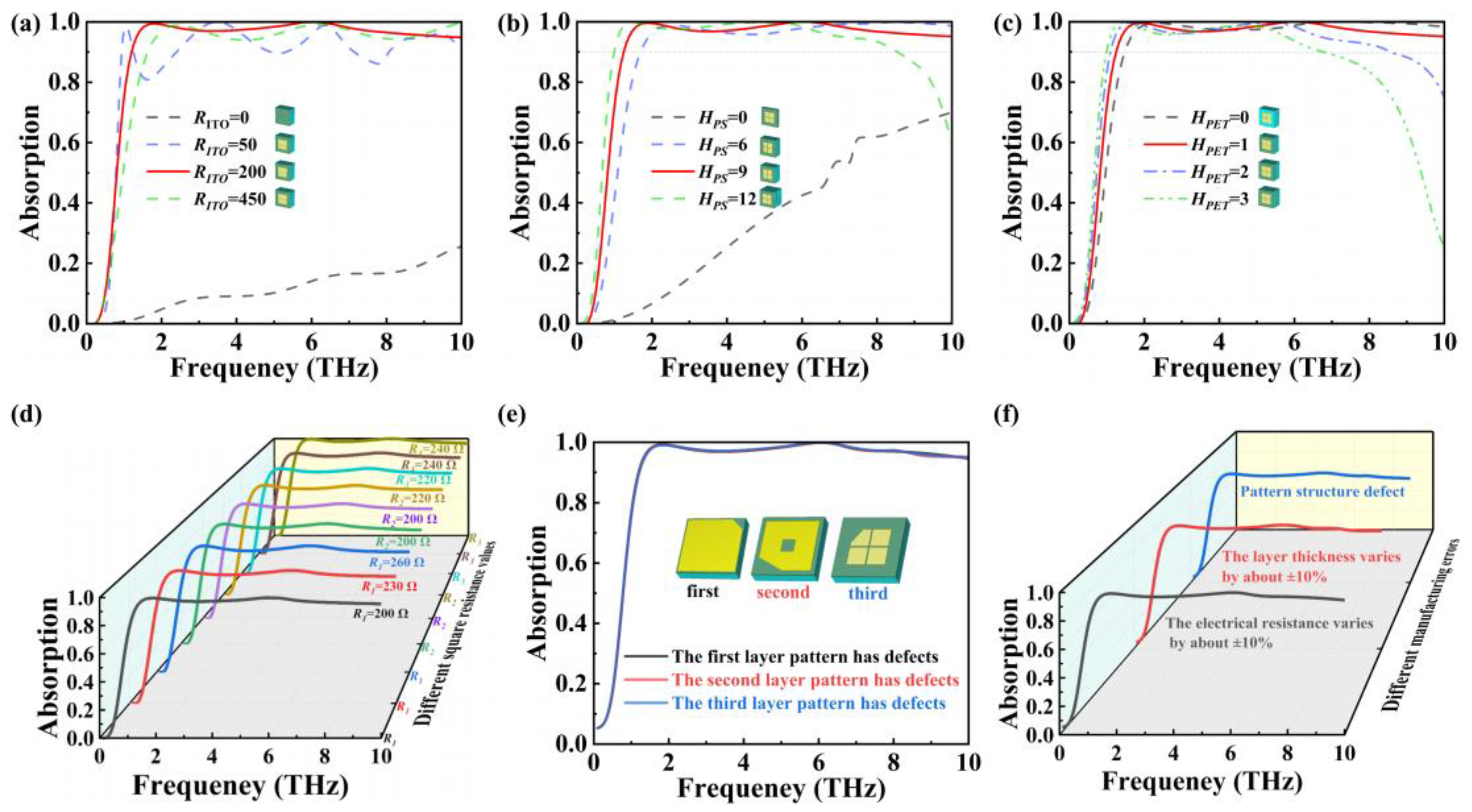
3.2. Loss Analysis of Dielectric Layer and Top ITO Layer

Our proposed absorber achieves broadband absorption in the terahertz band. We studied the surface loss, current distribution, and electromagnetic field distribution of the absorber at different peaks (Figure 4). Through simulation, it has been clarified that the main functions of each layer are the band and the absorption mechanism of each layer. As illustrated in Figure 4, induced currents are generated within the ITO films under the influence of electromagnetic fields. Due to the inherent square resistance (i.e., resistance per unit area) of the ITO films, energy loss primarily manifests as resistance loss when these currents traverse the film. As the current flows through the ITO thin-film structure, the incident THz waves gradually dissipate in the form of heat, thereby constituting the primary electromagnetic loss mechanism of this absorber. In the low-frequency range (Figure 4a,b), as the phase of the incident THz wave varies, a peak current emerges in the surface current distribution of the multi-layered structure. The direction of the current is indicated by the arrows in the figure. At the intermediate frequency of THz waves, around 6.0 THz, the electromagnetic loss structure responsible for perfect absorption is mainly concentrated within a specific ITO layer among the multi-layers (Figure 4c). For the incident high-frequency THz wave, as the phase of the incident wave varies, the surface current distribution is predominantly concentrated within the second and third ITO layers, as illustrated in Figure 4d. A systematic analysis of surface loss mechanisms and surface current distributions discloses that the lowermost ITO layers exert a predominant influence on the low-frequency absorption performance. This is primarily because they serve as the initial interface with incident THz waves, directly determining the energy transfer efficiency at the entry point. The middle ITO layers, in turn, play a decisive role in dictating mid-frequency absorption loss. Their position within the overall structure forms the core interaction zone, where the incident electromagnetic field undergoes significant transformation, thereby resulting in substantial energy dissipation. Meanwhile, the uppermost ITO layers, especially the patch-like structures, critically shape the high-frequency absorption of THz waves. These structures, with their unique geometric resonance characteristics, act as frequency-selective elements that selectively enhance absorption at specific high-frequency bands.
Based on the simulation results, the size of each layer of ITO structure was further optimized, and the size parameters proposed in this paper were finally determined. According to Figure 5, the bottom ITO mainly affects the absorption performance in the low-frequency range, the middle layer mainly acts on the mid-frequency range, and the four small ITO patches on the top layer regulate the absorption characteristics in the high-frequency range. As shown in Figure 5a, as L1 increases, the resonance point absorption rate of the first absorption band shows a trend of first increasing and then decreasing, while the absorption rate increases with the increase in R1 (Figure 5b). However, the size and resistance of the second ITO square ring layer have different effects on the resonance point and absorption rate in the mid-frequency band compared to the first ITO layer. As the size increases, the resonance point of the second layer structure undergoes a blue shift, and the absorption rate reaches its peak at a square resistance of 200 Ω/sq, as shown in Figure 5c,d. From Figure 5e,f, it can be seen that the resonance point of the third layer ITO, i.e., the top-layer structure, undergoes a blue shift with the increase in L3, but the absorption rate decreases with the increase in R3. Although simulation calculations show that S11 is significantly lower than 48 μm when L1 is 12 μm, it is based on sacrificing bandwidth. In addition, during the multi-layer stacking coupling process, the low-frequency absorption rate is further optimized and improved due to the increase in the subsequent two-layer architecture.
Furthermore, to more thoroughly investigate the role of each functional layer in the absorption performance and assess the feasibility of the absorber, simulations were carried out, as illustrated in Figure 6. As depicted in Figure 6a,b, the absence of the ITO resistance loss layer and the PS dielectric layer renders the device incapable of achieving absorption. This indicates that the ITO and PS layers serve as the primary functional layers responsible for high-performance absorption in the absorber. As illustrated in Figure 6c, the main function of the PET layer is to provide mechanical connection. A PET layer with a thickness of 1 μm has a negligible impact on the overall performance of the device. To further explore the influence of various critical parameters on the device’s performance, the ITO square resistance (RITO), PS thickness (HPS), and PET thickness (HPET) were optimized independently. The simulation results (Figure 5; Figure 6) reveal that when RITO = 200 Ω, HPET = 1 μm, and HPS = 9 μm, the device exhibits both feasibility and optimal absorption performance. Additionally, considering the process error in ITO resistance control, simulations were carried out for different ITO resistance values in each layer (as shown in Figure 6d). The results indicate that the ITO resistance loss layer with a resistance value of approximately 200 Ω has a negligible effect on the overall absorption performance. In addition, considering the existence of process errors in the actual preparation process, such as the thickness of the dielectric layer material, ITO square resistance, ITO pattern defects, etc., relevant simulations were carried out. The results indicate that changes in resistance values (Figure 6d,f) and changes in the dielectric layer thickness (Figure 6f) within a range of ±10% have minimal impact on the device’s absorption effect. The problem of ITO pattern defects, in the case of incomplete edges and corners (Figure 6e), will only have an impact in the 7–10 THz high-frequency range but can still maintain efficient absorption of over 90%. This lays the foundation for the preparation of the next perfect absorber in physical form.

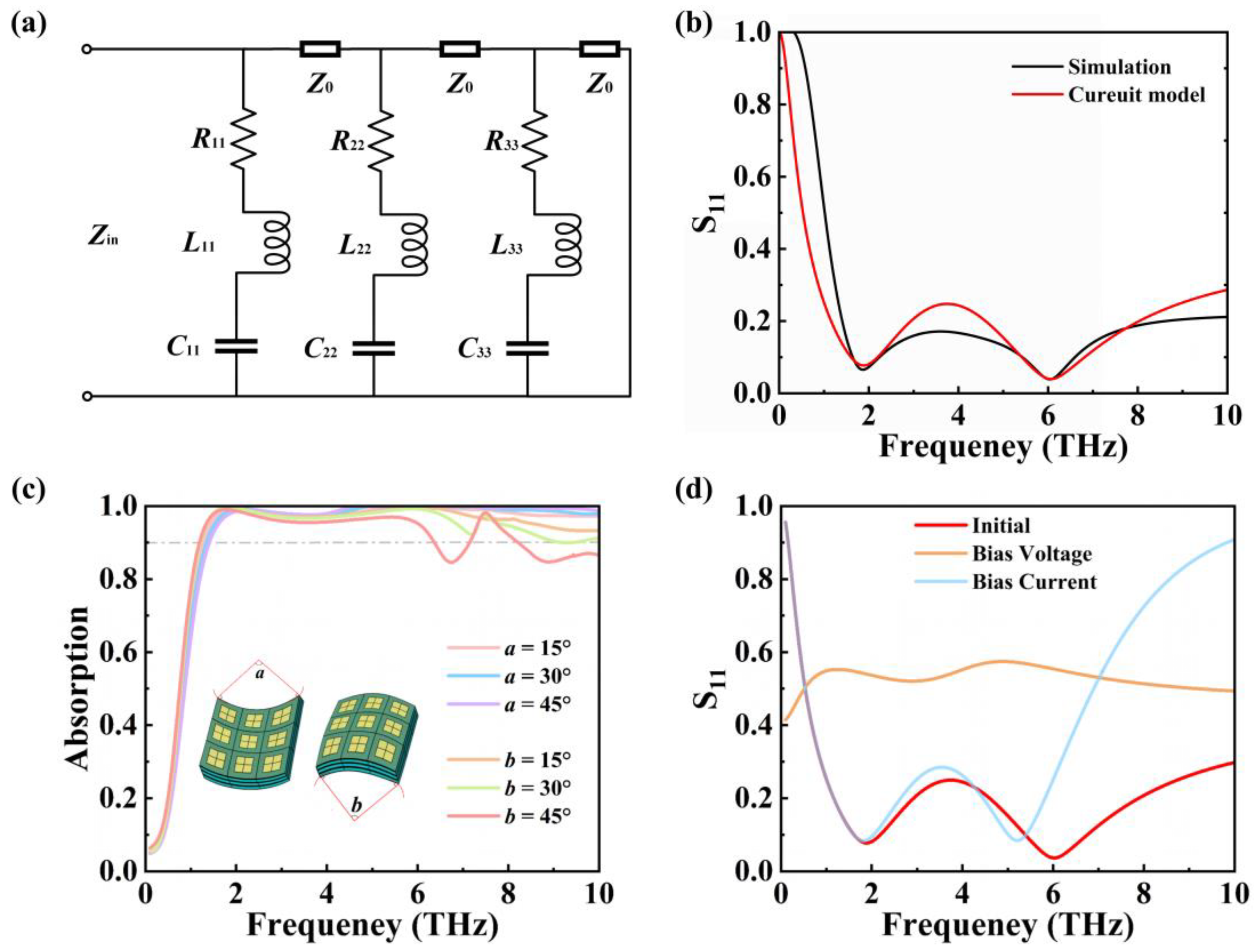
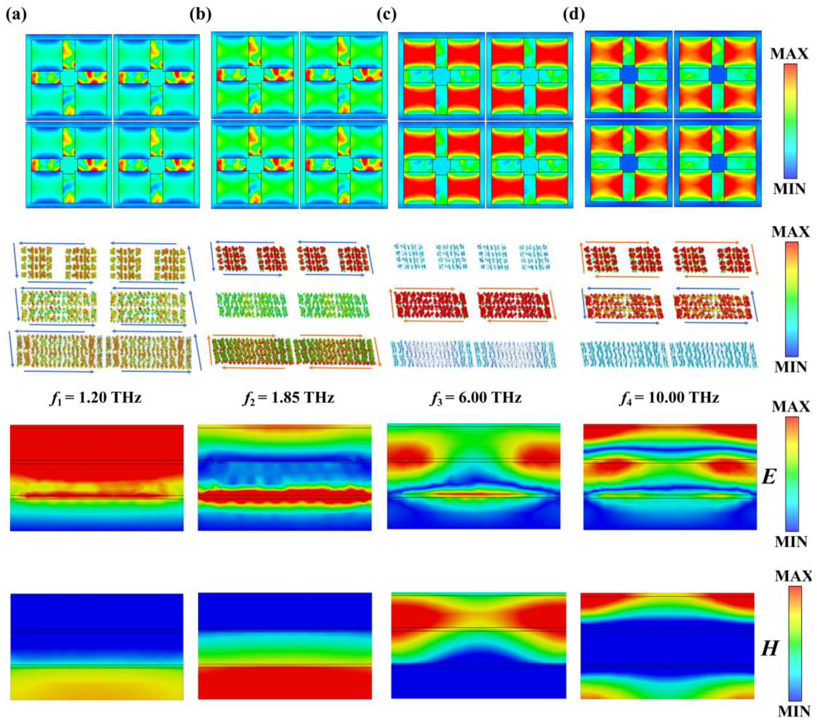
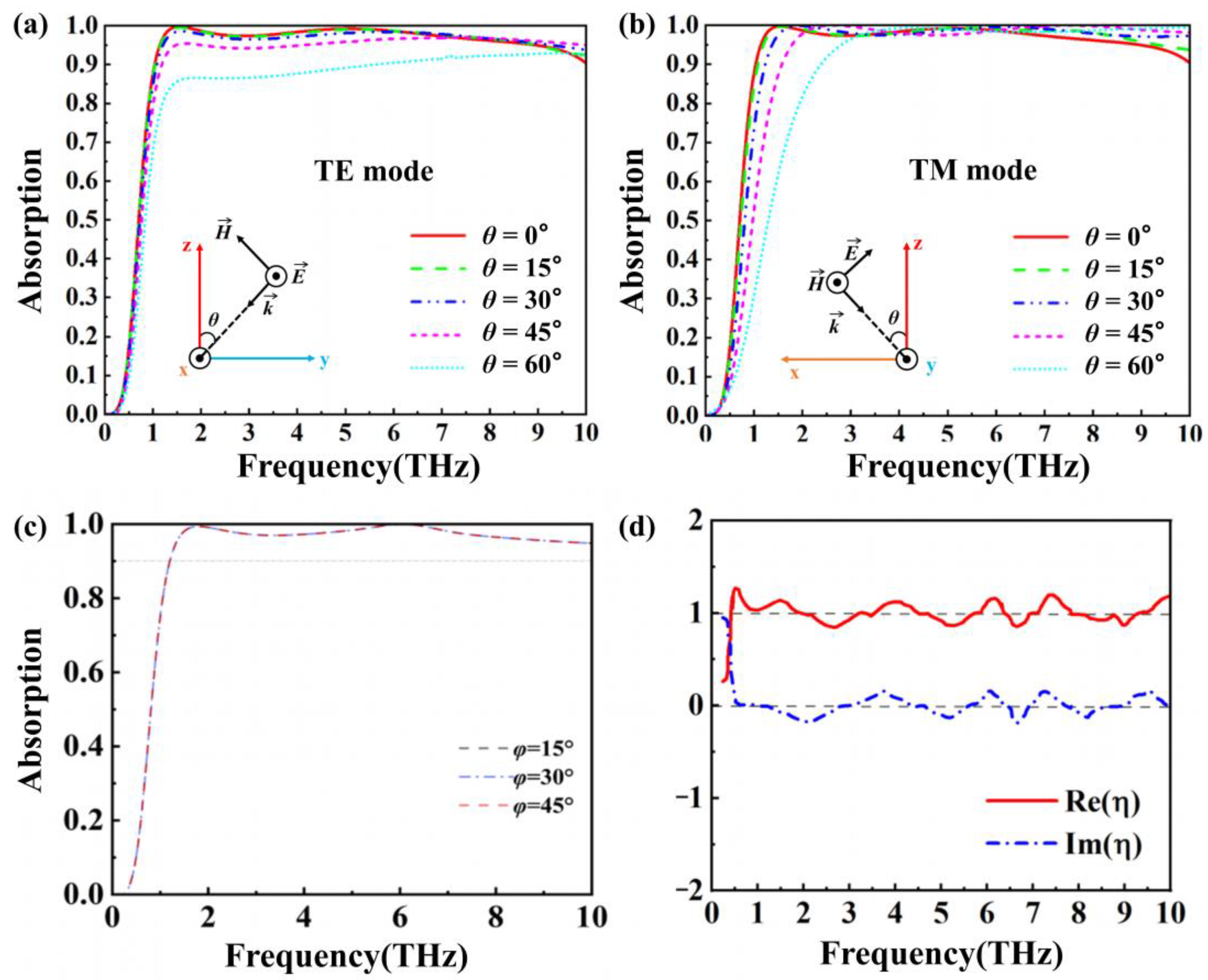
3.3. Analysis of Wide-Angle Absorption and Polarization Insensitivity

In terahertz absorbers, Transverse electric (TE) polarization mode refers to the electric field direction perpendicular to the incident plane and the magnetic field direction within the incident plane. Transverse magnetic (TM) polarization mode refers to the magnetic field direction being perpendicular to the incident plane, while the electric field direction is within the incident plane. The electromagnetic field distributions of these two modes are different (inset in Figure 7), resulting in differences in the response of the absorber to them [9]. Therefore, when designing terahertz absorbers, it is necessary to optimize the performance of the TE and TM modes separately to meet the requirements of different polarized incident waves. To validate the characteristics of the proposed absorber, the absorption performance of the absorber under large incident angles was investigated. In the simulation, a periodic array was constructed based on the unit cell, and obliquely incident THz waves were excited. As depicted in Figure 7a, for the TE mode of incidence, as the incident angle gradually increases from 0° to 45° in the z-plane, the material maintains a high absorption rate (above 90%), indicating good angular stability. However, when the incident angle further rises to 60°, the absorption rate exhibits a slight decline, dropping to above 80%. This finding holds significant reference value for the understanding and design of wide-angle absorbing materials. In contrast, for the TM mode, as the incident angle increases, the absorber achieves stable (greater than 90%) perfect absorption within the incident angle range of 0–60°, and the equivalent impedance slightly decreases (as shown in Figure 7b). When the incident angle reaches 60°, the equivalent impedance of the absorber increases, leading to a slight decrease in the impedance matching between the absorber and air. Consequently, the absorption rate in the TE mode decreases with an increasing incident angle, although it remains above 80%. The underlying cause of this phenomenon is attributed to the distinct variations in equivalent impedance between the two modes, which can be mathematically described by the following Equations (9) and (10) [34,35]:
η T E = η cos θ
η T M = η × cos θ
As illustrated in Figure 7c, we carried out a simulation analysis on the rotating incident wave, varying the rotation angle from 0° to 45° with a step size of 15°. In view of the quadruple rotational symmetry of the structure proposed in this study, it is evident that THz waves exhibit polarization stability under vertical incidence. The simulation results align well with the theoretical predictions, revealing that the four corresponding curves are highly consistent. This indicates that the absorber exhibits polarization insensitivity and retains polarization stability. Figure 7d presents the curves of the normalized real and imaginary parts of the absorber’s impedance, which are derived from the S parameters (Formula (3)) [36]. The absorber’s impedance exhibits characteristic behavior, with its real component oscillating approximately at one, while the imaginary component stabilizes near zero. This phenomenon indicates that the impedance of the absorber is well matched with the intrinsic impedance in free space. This systematic impedance transition, emerging from the synergistic interplay among the layers of the multi-layer foam structure, facilitates a nearly ideal input impedance matching across an extended frequency range.
Collectively, the THz absorber developed in this study demonstrates dual functional superiority: broadband angular insensitivity and robust polarization independence. The terahertz broadband absorbing metamaterial we designed can maintain good performance under oblique incidence (0–60°) in both the TE and TM polarization modes, mainly relying on its non-resonant impedance matching mechanism and the synergistic effect of the multi-layer structure. On the one hand, the ITO layer that achieves resistive loss is an angle-independent Ohmic loss, which can continuously dissipate energy as long as the electric field component (E-field) exists, regardless of the incident angle. On the other hand, the dielectric loss of the absorber is mainly dissipated through multiple reflections and interferences, with weak dependence on the angle. In this work, the total thickness of the dielectric layer is only 10 μm, which is much smaller than the terahertz wavelength of λ ≈ 300 μm@1THz, resulting in minimal additional phase delay when subjected to oblique incidence. Traditional absorbers suffer from severe phase mismatch when subjected to oblique incidence due to their large thickness, while our design avoids this problem through an ultra-thin structure. Furthermore, the Fabry–Perot cavity formed by the bottom ITO reflective layer and the surface ITO layer exhibits slight changes in interference conditions under oblique incidence. However, due to the extremely thin dielectric layer, multiple stacking further smooths the frequency response and reduces the angle sensitivity. This design avoids the angular limitations of magnetic resonance and provides a lightweight, wide-angle stable solution for terahertz broadband absorbers.

4. Conclusions

This article conducts a pure simulation work and proposes a lightweight THz planar absorber based on a multi-layer ITO structure, which demonstrates polarization insensitivity across an ultra-wideband frequency range. The research results indicate that the absorber attains highly efficient absorption, with an absorption rate surpassing 90% within the 1.2–10 THz range and exceeding 99.9% in certain frequency bands. Through the integration of equivalent circuit analysis, surface loss assessment, surface current distribution analysis, and impedance matching theory, the absorption mechanism of the absorber has been comprehensively investigated. It is unveiled that the absorber’s capacity to maintain polarization insensitivity while achieving robust absorption over a broad frequency spectrum is ascribed to the quadruple symmetry and the coupling effect of the proposed multi-layer structure. Moreover, the designed absorber not only exhibits polarization insensitivity but also shows excellent wide-angle absorption performance (within the 0–60° range). Additionally, it features a lightweight design and is easy to integrate, providing novel design concepts for applications such as military stealth technology, energy harvesting, and sensing and detection in the THz band.

Author Contributions

Conceptualization, Y.H. and T.L. (Tengteng Li); methodology, Y.H. and J.Y.; software, Y.H. and P.Z.; validation, P.Z., F.M. and H.W.; formal analysis, T.L. (Ting Liang); investigation, F.M.; resources, T.L. (Ting Liang); data curation, Y.H. and P.Z.; writing—original draft preparation, Y.H.; writing—review and editing, T.L. (Tengteng Li); visualization, Y.H. and H.W.; supervision, C.L.; project administration, C.L. and T.L. (Ting Liang); funding acquisition, M.L., T.L. (Tengteng Li) and Y.H. All authors have read and agreed to the published version of the manuscript.

Funding

This research was funded by the National Natural Science Foundation of China, grant numbers 62301509 and 62405293; the Fundamental Research Program of Shanxi Province, grant number 202203021222079; and the Graduate Research Innovation Project in Shanxi Province, grant number 2024KY589.

Institutional Review Board Statement

The study did not require ethical approval.

Informed Consent Statement

The study not involving humans.

Data Availability Statement

The data are available on reasonable request from the corresponding author.

Conflicts of Interest

The authors declare no conflicts of interest.

Abbreviations

The following abbreviations are used in this manuscript:
THzTerahertz
PSPolystyrene
PETPolyethylene terephthalate
ITOIndium tin oxide
TETransverse electric
TMTransverse magnetic

References

  1. Yao, J.Q.; Li, J.; Zhang, Y.T.; Ding, X.; Wu, L. Technology for terahertz wave manipulation: Harnessing the light of terahertz. Chin. J. Nat. 2023, 45, 1–16. [Google Scholar]
  2. Liang, D.C.; Wei, M.G.; Gu, J.Q.; Yin, Z.P.; Ouyang, C.M.; Tian, Z.; He, M.X.; Han, J.G.; Zhang, W.L. Broad-band time domain terahertz radar cross-section research in scale models. Acta Phys. Sin. 2014, 63, 214102. [Google Scholar] [CrossRef]
  3. Matsumoto, H.; Watanabe, I.; Kasamatsu, A.; Monnai, Y. Integrated terahertz radar based on leaky-wave coherence tomography. Nat. Electron. 2020, 3, 122–129. [Google Scholar] [CrossRef]
  4. Chen, H.; Ma, W.; Huang, Z.; Zhang, Y.; Huang, Y.; Chen, Y. Graphene-Based Materials toward Microwave and Terahertz Absorbing Stealth Technologies. Adv. Opt. Mater. 2019, 7, 1801318. [Google Scholar] [CrossRef]
  5. Sun, B.; Huang, L.R.; Ding, J.F.; Luo, Y.; Zhang, Y.Z.; Li, R.Z.; Wang, X.C.; Wen, Q.Y.; Xiao, S.Y. Flexible and transparent metadevices for terahertz, microwave, and infrared multispectral stealth based on modularization design. Opt. Express 2023, 31, 8650–8667. [Google Scholar] [CrossRef]
  6. Jin, Y.; Yu, H.; Wang, Y.; Wang, L.; Nan, B. Recent Progress in Electromagnetic Wave Absorption Coatings: From Design Principles to Applications. Coatings 2024, 14, 607. [Google Scholar] [CrossRef]
  7. Liu, Y.P.; Dong, L.; Sabri, M.F.M.; Majid, N.A.; Ibrahim, S. Advancements in tunable and multifunctional metamaterial absorbers: A comprehensive review of microwave to terahertz frequency range. J. Phys. D Appl. Phys. 2024, 57, 293002. [Google Scholar] [CrossRef]
  8. Chen, H.T.; Taylor, A.J.; Yu, N.F. A review of metasurfaces: Physics and applications. Rep. Prog. Phys. 2016, 7, 076401. [Google Scholar] [CrossRef]
  9. Li, F.J.; Wang, S.; Zhong, R.; Hu, M.X.; Jiang, Y.; Zheng, M.J.; Wang, M.; Li, X.P.; Peng, R.W.; Den, Z.L. Metasurface polarization optics: From classical to quantum. Appl. Phys. Rev. 2024, 11, 041332. [Google Scholar] [CrossRef]
  10. Ji, L.; Varadan, V.V. Negative refractive index and negative refraction of waves in lossy metamaterials. Electron. Lett. 2016, 52, 260–261. [Google Scholar] [CrossRef]
  11. Cai, T.; Zheng, B.; Lou, J.; Shen, L.; Yang, Y.; Tang, S.; Li, E.; Qian, C.; Chen, H. Experimental Realization of a Superdispersion-Enabled Ultrabroadband Terahertz Cloak. Adv. Mater. 2022, 34, 2205053. [Google Scholar] [CrossRef]
  12. Zhang, Q.; Li, G.; Wu, L.; Yang, F.; Yue, Z.; Zheng, C.; Zhang, Y.; Li, L.; Yao, J.Q. Chip-integrated polarization multiplexed metasurface for simultaneous generation of versatile terahertz vortices. Nanophotonics 2025, 14, 2219–2228. [Google Scholar] [CrossRef] [PubMed]
  13. Xiang, X.C.; Feng, L.C.; Yang, S.X.; Zhang, W.; Zhang, C.H.; Wu, J.B.; Fan, K.; Jin, B.B.; Chen, J.; Wang, H.B.; et al. Focusing enhancement of terahertz surface plasmon polaritons. Appl. Phys. Lett. 2023, 122, 151101. [Google Scholar] [CrossRef]
  14. Zhang, T.; Guo, T.M.; Yan, J.Y.; Pei, Y.A. Design of Tunable Four-Broadband Terahertz Absorber. Acta Opt. Sin. 2024, 44, 0523002. [Google Scholar]
  15. Cheng, X.; Huang, R.; Xu, J.; Xu, X. Broadband Terahertz Near-Perfect Absorbers. ACS Appl. Mater. Interfaces 2020, 12, 33352–33360. [Google Scholar] [CrossRef] [PubMed]
  16. Paddubskaya, A.; Novitsky, A.; Valynets, N.; Kumar, M.; Itkonen, T.; Pekkarinen, M.; Soboleva, E.; Lahderanta, E.; Kafesaki, M.; Svirko, Y.; et al. All-graphene perfect broadband THz absorber. Carbon 2021, 185, 709–716. [Google Scholar] [CrossRef]
  17. Zeng, D.; Zong, S.; Liu, G.; Yuan, W.; Liu, X.; Liu, Z. Dynamically electrical/thermal-tunable perfect absorber for a high-performance terahertz modulation. Opt. Express 2022, 30, 39736–39746. [Google Scholar] [CrossRef]
  18. Zhang, K.; Xia, F.; Li, S.; Liu, Y.; Kong, W. Actively tunable multi-band terahertz perfect absorber due to the hybrid strong coupling in the multilayer structure. Opt. Express 2021, 29, 28619–28630. [Google Scholar] [CrossRef]
  19. Yi, N.N.; Zong, R.; Gong, J.; Duan, T.; Qian, R.R. Single-/Dual-Band Switchable Terahertz Absorber Based on Vanadium Dioxide-Dirac Semi-Metal Hybrid Metamaterial. Chin. J. Lasers 2022, 49, 0314002. [Google Scholar]
  20. Meng, T.; Hu, D.; Zhu, Q. Design of a five-band terahertz perfect metamaterial absorber using two resonators. Opt. Commun. 2018, 415, 151–155. [Google Scholar] [CrossRef]
  21. Wang, T.L.; Qu, L.Z.; Qu, L.F.; Zhang, Y.P.; Zhang, H.Y.; Cao, M.Y. Tunable broadband terahertz metamaterial absorber using multi-layer black phosphorus and vanadium dioxide. J. Phys. D Appl. Phys. 2020, 53, 145105. [Google Scholar] [CrossRef]
  22. Wang, B.X.; Duan, G.Y.; Xu, C.Y.; Jiang, J.Y.; Xu, W.; Pi, F.W. Design of multiple-frequency-band terahertz metamaterial absorbers with adjustable absorption peaks using toothed resonator. Mater. Des. 2023, 225, 111586. [Google Scholar] [CrossRef]
  23. Rengasamy, S.; Natarajan, R.; Kuttathati Srinivasan, V. Miniaturized Multi-Spectral Perfect Metamaterial Absorber for THz Sensing, Imaging and Spectroscopic Applications. Plasmonics 2023, 18, 643–651. [Google Scholar] [CrossRef]
  24. Qi, L.; Liu, C.; Shah, S.M.A. A broad dual-band switchable graphene-based terahertz metamaterial absorber. Carbon 2019, 153, 179–188. [Google Scholar] [CrossRef]
  25. Ali, A.; Mitra, A.; Aïssa, B. Metamaterials and Metasurfaces: A Review from the Perspectives of Materials, Mechanisms and Advanced Metadevices. Nanomaterials 2022, 12, 1027. [Google Scholar] [CrossRef] [PubMed]
  26. Wang, Y.Z.; Xu, H.X.; Wang, C.H.; Wang, M.Z.; Wang, S.J. Research progress of electromagnetic metamaterial absorbers. Acta Phys. Sin. 2020, 69, 134101. [Google Scholar] [CrossRef]
  27. Li, S.J.; Wu, P.X.; Xu, H.X.; Zhou, Y.L.; Cao, X.Y.; Han, J.F.; Zhang, C.; Yang, H.H.; Zhang, Z. Ultra-wideband and Polarization-Insensitive Perfect Absorber Using Multilayer Metamaterials, Lumped Resistors, and Strong Coupling Effects. Nanoscale Res. Lett. 2018, 13, 386. [Google Scholar] [CrossRef]
  28. Xiao, D.Y.; Zhu, M.M.; Wang, Q.; Sun, L.M.; Zhao, C.; Ng, Z.K.; Teo, E.H.T.; Hu, F.J.; Tu, L.C. A flexible and ultra-broadband terahertz wave absorber based on graphene-vertically aligned carbon nanotube hybrids. Mater. Chem. C 2020, 8, 7244–7252. [Google Scholar] [CrossRef]
  29. Zhao, G.Z.; Mors, M.T.; Wenckebach, T.; Planken, P.C.M. Terahertz dielectric properties of polystyrene foam. J. Opt. Soc. Am. B 2002, 19, 1476–1479. [Google Scholar] [CrossRef]
  30. Wen, Q.Y.; Xie, Y.S.; Zhang, H.W.; Yang, Q.H.; Li, Y.X.; Liu, Y.L. Transmissionline model and fields analysis ofmetamaterial absorber in the terahertz band. Opt. Express 2009, 17, 20256–20265. [Google Scholar] [CrossRef] [PubMed]
  31. Notaros, B.M. Electromagnetics; Prentice Hall: Upper Saddle River, NJ, USA, 2011. [Google Scholar]
  32. Holm, R.T. Handbook of Optical Constants of Solids; Academic Press: Cambridge, MA, USA, 1998. [Google Scholar]
  33. Costa, F.; Monorchio, A.; Manara, G. Efficient Analysis of Frequency-Selective Surfaces by a Simple Equivalent-Circuit Model. IEEE Antennas Propag. Mag. 2012, 54, 35–48. [Google Scholar] [CrossRef]
  34. Yuan, X.; Xu, Y.; Chen, M.; Cheng, X.; Fang, D. Blocking gate resonator rasorber surface brings wide band electromagnetic absorption performance approaching theoretical limit. Microw. Opt. Technol. Lett. 2019, 61, 1524–1528. [Google Scholar] [CrossRef]
  35. Wheeler, H. Simple relations derived fom a phased-array antenna made of an infinite current sheet. IEEE Trans. Antennas Propag. 1965, 13, 506–514. [Google Scholar] [CrossRef]
  36. Smith, D.R.; Vier, D.C.; Koschny, T.; Soukoulis, C.M. Electromagnetic parameter retrieval from inhomogeneous metamaterials. Phys. Rev. E 2005, 71, 036617. [Google Scholar] [CrossRef] [PubMed]
Figure 1. Structural diagram of ultra-wideband absorber. (a) Schematic of complete array; (b) Side view of unit cell and absorption mechanism schematic; (c) Single-unit explosion diagram.
Photonics 12 00787 g001
Figure 2. Comparison diagram of reflection losses under different combination structures of ultra-wideband absorbers. Reflection loss results for (a) the structure 1; (b) the structure 2; (c) the structure 3; (d) the structure 1&2; (e) the structure 1&3; (f) the structure 2&3; (g) the structure 1&2&3 (this article); (h) comparison chart of reflection loss results for each layer; (i) each structure’s absorption bandwidth and peak absorption rate.
Photonics 12 00787 g002
Figure 3. (a) Equivalent circuit diagram of unit structure; (b) The comparison of the S11 curve obtained by CST simulation and ADS circuit simulation; (c) Absorption results of metamaterials after bending (The gray dashed line represents 90% absorption.); (d) Absorption results of metamaterials after applying bias voltage/current.
Photonics 12 00787 g003
Figure 4. The surface loss, surface current distributions, electric field distributions, and magnetic field distributions of the proposed absorber at (a) 1.2 THz, (b) 1.85 THz, (c) 6.0 THz, and (d) 10.0 THz.
Photonics 12 00787 g004
Figure 5. The first-layer structure S11 varies with (a) the size L1 of the bottom square ITO layer and (b) the resistance R1. The thickness of (c) the first layer of foam H1. The second-layer structure S11 varies with (d) the size L2 of the annular ITO layer and (e) the resistance R2. (f) The thickness of the first layer of foam H2. The third-layer structure S11 varies with (g) the size L3 of the four small square ITO layers and (h) the resistance R3. (i) The influence of the thickness of the first layer of foam H3 on S11.
Photonics 12 00787 g005
Figure 6. Simulation analysis of absorption effect after parameter changes in each functional layer. (a) ITO layer analysis; (b) PS layer analysis; (c) PET layer analysis; (d) Analysis of Square Resistance of ITO Layer; (e) Simulation of the absorption effect of an absorber in a device with repeated pattern errors or defects; (f) Absorption effect simulated for the dielectric layer thickness or resistance varies by about ±10%.
Photonics 12 00787 g006
Figure 7. Absorption characteristics under different incident angles and polarized light. Absorption rate varies with incident angle in (a) TM and (b) TE polarization modes. (c) Absorption rate at different polarization angles. (d) The curve of the normalized real and imaginary parts of impedance obtained by deriving S absorption parameters.
Photonics 12 00787 g007
Table 1. Parameter values in RLC equivalent circuit.
ParameterValue
R1121 Ω
L1180 fH
C110.53 fF
R2254 Ω
L223.16 pH
C220.38 fF
R3347 Ω
L333.25 pH
C335.03 fF
Disclaimer/Publisher’s Note: The statements, opinions and data contained in all publications are solely those of the individual author(s) and contributor(s) and not of MDPI and/or the editor(s). MDPI and/or the editor(s) disclaim responsibility for any injury to people or property resulting from any ideas, methods, instructions or products referred to in the content.

