Article

A Perovskite-Based Photoelectric Synaptic Transistor with Dynamic Nonlinear Response

1
College of Information Science and Engineering, Huaqiao University, Xiamen 361021, China
2
National & Local United Engineering Laboratory of Flat Panel Display Technology, Fuzhou University, Fuzhou 350108, China
*
Authors to whom correspondence should be addressed.
Photonics 2025, 12(7), 734; https://doi.org/10.3390/photonics12070734
Submission received: 15 June 2025 / Revised: 1 July 2025 / Accepted: 16 July 2025 / Published: 18 July 2025
(This article belongs to the Special Issue Polaritons Nanophotonics: Physics, Materials and Applications)

Abstract

Nonlinear characteristics are essential for neuromorphic devices to process high-dimensional and unstructured data. However, enabling a device to realize a nonlinear response under the same stimulation condition is challenging as this involves two opposing processes: simultaneous charge accumulation and recombination. In this study, a hybrid transistor based on a mixed-halide perovskite was fabricated to achieve dynamic nonlinear changes in synaptic plasticity. The utilization of a light-induced mixed-bandgap structure within the mixed perovskite film has been demonstrated to increase the recombination paths of photogenerated carriers of the hybrid film, thereby promoting the formation of nonlinear signals in the device. The constructed heterojunction optoelectronic synaptic transistor, formed by combining a mixed-halide perovskite with a p-type semiconductor, generates dynamic nonlinear decay responses under 400 nm light pulses with an intensity as low as 0.02 mW/cm2. Furthermore, it has been demonstrated that nonlinear photocurrent growth can be achieved under 650 nm light pulses. It is important to note that this novel nonlinear response is characterized by its dynamism. These improvements provide a novel method for expanding the modulation capability of optoelectronic synaptic devices for synaptic plasticity.

1. Introduction

Neuromorphic computing is expected to overcome the limitations of existing von Neumann computers [1,2,3,4,5,6,7]. An important feature of neuromorphic computing is its ability to simulate information transmission and processing in human brain neural networks [5,6,8]. In natural environments, the human brain often needs to process complex, spatially scaled information [9,10,11]. Neuromorphic computing based on a single linear model struggles to effectively acquire and process dynamic data under different scenarios [1,9]. In neuromorphic systems, this nonlinear behavior facilitates the recognition of multiscale signals in space, such as optical mixed signals and static/dynamic signals [9,12]. These can be applied to neuromorphic visual sensors to achieve higher-resolution spatial imaging. Therefore, nonlinear dynamics are essential for neuromorphic systems to process unstructured data and dynamic spatiotemporal patterns. In recent years, researchers have attempted to develop neuromorphic hardware systems incorporating external negative feedback circuits in order to achieve nonlinearity [13,14,15,16]. However, these circuits cannot autonomously adjust thresholds in response to dynamic environmental changes, and their reliance on external components increases system energy consumption and complexity. Nonlinear activation functions achieved through device-level physical phenomena significantly simplify hardware architectures by obviating external signal conversion circuits. Therefore, the development of devices with nonlinear characteristics is essential for neuromorphic systems to accurately reproduce the complex dynamics of biological synaptic behaviors. Photoelectric synaptic transistors, which use light signals to directly modify device synaptic weights, have become a research hotspot in the field of neuromorphic devices due to advantages such as wireless communication and ultra-fast signal transmission [1,2,17,18,19,20]. Currently, most reported artificial synaptic transistors modulate the conduction channel’s conductance using external stimuli to simulate plasticity. Most of these devices require switching between different external stimulation conditions to simulate synaptic excitation and inhibition. For instance, electrical synapses require distinct bias voltages for excitation and inhibition [14,21,22], photoelectric synapses employ light stimulation for excitation and reverse electrical stimulation to modulate conductance for inhibition [2,20,23,24,25,26,27], and all-optical synapses necessitate different wavelengths or intensities of light to induce excitation and inhibition [28,29,30,31]. The need to switch stimulation conditions for inhibition limits the ability of synaptic devices to achieve a nonlinear response through autonomous negative feedback regulation. Previously, researchers proposed a scheme involving strong light coupling with electrical stimulation to induce carrier trapping and form a reverse built-in electric field that shields the gate voltage [9]. This successfully achieves simultaneous synaptic excitation and inhibition, thereby simulating homeostatic plasticity. Nevertheless, it is challenging to enable a device to demonstrate a nonlinear response under the same stimulation condition. This is due to the requirement of two opposing processes, namely excitation and inhibition, to occur simultaneously.
In this study, we present a CsPbBr2.4I0.6-based hybrid synaptic photoelectric transistor exhibiting dynamic nonlinear responses. The introduction of photoinduced mixed-bandgap capturing of photogenerated carriers has been shown to enhance the abnormal changes in the device’s synaptic plasticity. Under illumination, the induced formation of a mixed-bandgap structure within the film increases the recombination paths of photogenerated carriers, thereby promoting the formation of nonlinear signals in the device. In order to comprehend the manner in which the mixed-bandgap structure impedes the flow of photocurrent, an analysis was conducted of the energy band diagram of the CsPbBr2.4I0.6-based device structure. Furthermore, a comparison was made between the transfer characteristic curves and postsynaptic current (PSC) variation trends of CsPbBr2.4I0.6-based devices and those of CsPbBr3-based devices under light stimulation. Finally, the generation of dynamic nonlinear decay responses was achieved with a mere 0.02 mW/cm2 of 400 nm light pulses. Furthermore, it was demonstrated that 650 nm light pulses were also capable of inducing nonlinear photocurrent growth in the device. It is important to note that this novel nonlinear response is characterized by its dynamism. This work presents a novel approach to the promotion of efficient nonlinear models in neuromorphic devices.

2. Materials and Methods

2.1. Hybrid Transistor Fabrications

The 0.15 M CsPbBr2.4I0.6 precursor was acquired via the dissolution of PbBr2, CsI and CsBr in dimethyl sulfoxide, and the 0.15 M CsPbBr3 precursor was acquired via the dissolution of PbBr2 and CsBr in dimethyl sulfoxide. The CsPbBr2.4I0.6 and CsPbBr3 (preheated at 100 °C) precursors were utilized for spin-coating at 3000 rpm for 60 s under nitrogen atmospheres on a cleaned Si/SiO2 substrate, respectively. The resulting CsPbBr2.4I0.6 and CsPbBr3 films were then transferred to a pump chamber for removing the residual solvent. TIPS-pentacene and polystyrene were dissolved in chlorobenzene with a concentration of 10 mg/mL, respectively. For the fabrication of the p-type semiconductor, the precursor was prepared by mixing the IPS-pentacene and polystyrene solution with a volume ratio of 3: 1. The TIPS-pentacene film was deposited by dip coating on the CsPbBr2.4I0.6 and CsPbBr3 films under ambient conditions, respectively. Then, the hybrid films were baked at 100 °C for 30 min under a nitrogen atmosphere for crystallization. Finally, 50 nm thick gold electrodes with a channel length of 80 μm and width of 200 μm were formed by the shadow mask thermal evaporation method to fabricate the hybrid devices.

2.2. Characterizations

The morphological characteristics of the films were analyzed using an Olympus BX51M fluorescence microscope (Tokyo, Japan). Steady-state photoluminescence (PL) spectra were acquired with a F4600 spectrometer to evaluate photoelectric properties, while the electrical performance of the devices was characterized under ambient conditions via a Keithley 4200-SCS system (Tektronix, Beaverton, OR, USA).

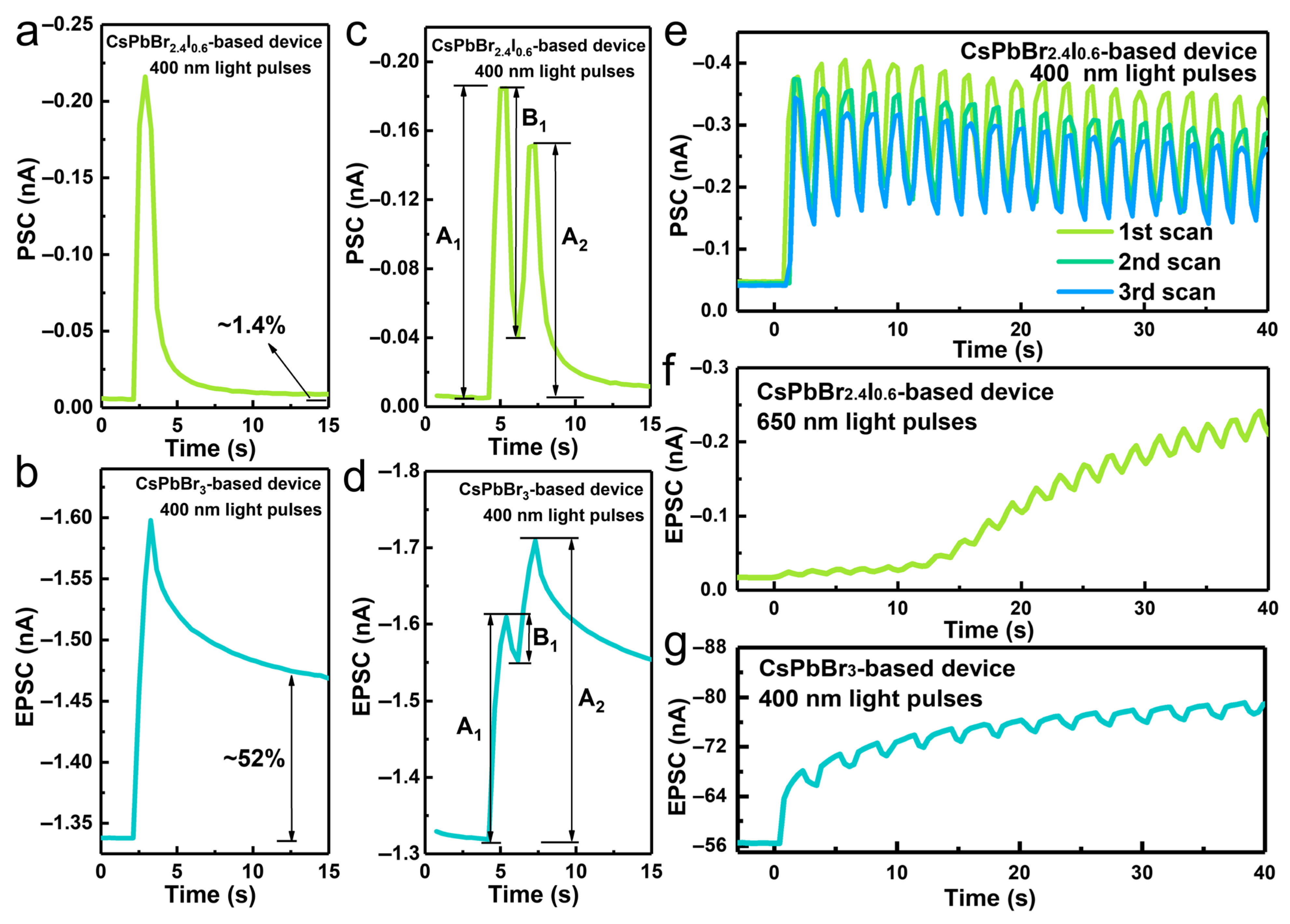
3. Results and Discussion

Synapses are the fundamental structural units involved in processing information in the human brain. When the brain receives complex spatial-scale information, it exhibits nonlinear characteristics during processing (see Figure 1a). Figure 1b shows the structure of a mixed-halide perovskite (CsPbBr2.4I0.6)/p-type semiconductor hybrid transistor. The CsPbBr2.4I0.6 layer acts as a light absorber, gradually forming narrowband and broadband mixed-bandgap structures when exposed to light. This structural feature is critical for generating dynamic nonlinear signals in the device. A p-type semiconductor layer is deposited on the perovskite layer to form a carrier transport layer and a type-II heterojunction with the perovskite, enabling current signals that mimic biological synaptic plasticity. As shown in Figure 1c, under fixed illumination, localized changes to this bandgap structure cause photogenerated carriers to recombine preferentially in the narrow-bandgap regions, thereby influencing charge transfer processes.
To investigate the dynamic changes under light exposure, the CsPbBr2.4I0.6 film and the CsPbBr3 film were tested utilizing the fluorescence microscope’s blue light illumination mode. As shown in Figure 2a, it was observed that the CsPbBr2.4I0.6 film predominantly emitted green light when subjected to 1 s of blue light irradiation. As the duration of blue light irradiation is increased from 8 to 13 s, a substantial increase in the number of narrow-band iodine-rich phases emitting red light within the film becomes evident. For the purpose of comparison, the CsPbBr3 film was also exposed to blue light. Figure 2b demonstrates that no significant alterations in the CsPbBr3 film were observed as the duration of blue light irradiation increased. This phenomenon of the formation of mixed bandgaps in the CsPbBr2.4I0.6 film with increasing illumination time was also confirmed by PL spectra. As illustrated in Figure 2c, the PL spectra of the CsPbBr2.4I0.6 film were examined under high-intensity ultraviolet (UV) light irradiation for varying durations. Prior to UV irradiation, the CsPbBr2.4I0.6 film displays a single emission peak at approximately 570 nm. When the irradiation time reaches one minute, the intensity of the emission peak at approximately 570 nm gradually decreases for the first time, while a new emission peak emerges at approximately 630 nm. As the irradiation time increases further, the peak intensity at around 570 nm continues to decrease and the emission peak at around 630 nm gradually shifts towards longer wavelengths and increases in intensity. Following a period of 12 minutes’ irradiation, a shift in the emission peak to approximately 660 nm was observed. This finding suggests that, upon exposure to prolonged UV light, the CsPbBr2.4I0.6 film evolves to exhibit mixed bandgaps, comprising both narrow and broad bands. The ratio of these two band types undergoes dynamic fluctuations as the illumination duration is increased. In order to verify the reversibility of this phenomenon, an investigation was conducted into the alterations in the CsPbBr0.4I0.6 film in the presence of green light and in the dark following the cessation of stimulation. As demonstrated by the fluorescence microscopy images in Figure S1, the region emitting red fluorescence in the CsPbBr0.4I0.6 film appeared to expand under the green light, indicating an increase in the existence of the narrow-bandgap phase. Conversely, when the film was stored in the dark for extended periods, there was a gradual decline in the narrow-bandgap phase. Furthermore, previous studies have confirmed via PL measurements that mixed-halide perovskites can recover from a phase-separated state to a mixed phase [32]. These findings indicate that the working mechanism of the device, which relies on perovskite phase separation, exhibits reversibility. PL spectra of the CsPbBr2.4I0.6 film, the TIPS-pentacene film, and the hybrid film were acquired to investigate the transport of photogenerated carriers (Figure 2d). The hybrid film exhibited distinct photoluminescence features, including a ~550 nm emission peak attributed to CsPbBr2.4I0.6 and a ~650 nm emission peak from the TIPS-pentacene. Notably, compared to the individual CsPbBr2.4I0.6 and TIPS-pentacene films, the hybrid film showed significant quenching of both emission peaks, suggesting efficient carrier separation at the CsPbBr2.4I0.6/TIPS-pentacene interface.
The present study investigates the impact of light-induced mixed-bandgap phenomena on the photosensitive performance of devices; the transfer characteristic curves of the devices under illumination were tested. As demonstrated in Figure 3a, the CsPbBr2.4I0.6-based device exhibited a substantial enhancement in photocurrent and a favorable shift in threshold voltage under 600 nm light illumination. As the gate voltage varied from 30 V to −40 V, the on/off ratio of the photocurrent to dark current gradually increased from approximately 2 to approximately 102, after which it slowly decreased to approximately 1. Since CsPbBr3 does not exhibit multiple bandgap structures under illumination, a comparative test was conducted using a CsPbBr3-based device with the same structure under 400 nm light illumination (Figure 3b). In a similar manner, the on/off ratio of the CsPbBr3-based device exhibited an initial increase from approximately 2 to ~104, subsequently decreasing gradually to 1. It is noteworthy that for the CsPbBr2.4I0.6-based device under 400 nm illumination, the on/off ratio initially increased from 7 to a maximum of approximately 103; however, the photocurrent growth rate rapidly decelerated and approached saturation. In circumstances where the gate voltage was below −26 V, the on/off ratio underwent a gradual decline, dipping below 1. This distinctive occurrence can be attributed to the presence of a mixed-bandgap structure that enabled photogenerated carriers to become trapped, thereby augmenting the photogating effect.
In order to understand how the mixed-bandgap structure inhibits the photogenerated current, the energy band diagram of the CsPbBr2.4I0.6-based device structure was analyzed in more detail. According to the previous studies, the conduction band minimum and valence band maximum of CsPbBr2.4I0.6 and TIPS-pentacene (a p-type semiconductor) were −5.92 eV (−5.3 eV) and −3.73 eV (−3.0 eV) [26,33]. Therefore, the CsPbBr2.4I0.6 film (acting as the light absorption layer) and the p-type semiconductor (acting as the carrier transport layer) form a type-II heterostructure (shown in Figure 4a). Before the formation of the mixed-bandgap structure, photogenerated excitons are produced when the CsPbBr2.4I0.6 film is stimulated by blue light. Due to the band offset at the heterojunction, the photogenerated holes then transfer to the p-type semiconductor, thereby increasing the device current. Conversely, photogenerated electrons gradually accumulate in the perovskite film due to interfacial barrier blocking. As blue light stimulation continues, a narrow-band iodine-rich phase emerges locally in the CsPbBr2.4I0.6 film. In the mixed-bandgap structure, photogenerated carriers are easily captured by the narrow-band region, thereby increasing the recombination pathways of photogenerated carriers. This implies that light stimulation can induce a dynamic competition mechanism in which photogenerated carrier generation and recombination coexist in the device. This phenomenon can be regarded as a coupling of current potentiation and inhibition, with the inhibitory behavior acting as a negative feedback mechanism (see Figure 4b). Figure 4c shows the PSC with nonlinear characteristics generated in the device after 20 blue light stimulations. To facilitate analysis of current variation trends, the peak current amplitude of responsive current growth after the nth light pulse is defined as An. As shown in Figure 4c, it can be seen that the current first increases from A1 to An and then decreases gradually (with the ratio A20/A1 being 0.82 < 1). This result indicates that the mixed-bandgap structure exerts inhibitory regulation.
In order to investigate the impact of research into mixed-bandgap structures on synaptic plasticity, we measured the PSCs of CsPbBr3-based and CsPbBr2.4I0.6-based devices under light stimulation. Figure 5a illustrates the PSC of a CsPbBr2.4I0.6-based device subjected to single-pulse stimulation. It can be seen that the PSC decays rapidly once the pulse has ceased. Over the same time period, the level of the excitatory postsynaptic current (EPSC) maintained by the CsPbBr3-based device (~52%) is significantly higher than that maintained by the CsPbBr2.4I0.6-based device (~1.4%), as shown in Figure 5b. Both CsPbBr2.4I0.6-based and CsPbBr3-based devices exhibit persistent photoconductance (PPC) phenomena [34,35,36] because the interfacial barrier blocked the recombination of photogenerated electrons trapped in the perovskite film after stimulation stopped. Figure 5c,d present the paired-pulse depression (PPD) and the paired-pulse facilitation (PPF) triggered by two consecutive light pulses in CsPbBr2.4I0.6-based and CsPbBr3-based devices, respectively. Due to the potential barrier, which prolongs and slows the recombination rate, the post-pulse decay levels (B1/A1) of the CsPbBr3-based device are ~33%, which is much smaller than those of CsPbBr2.4I0.6-based device (~78%). The current decay after light pulse cessation primarily arises from the recombination of photogenerated electrons and holes. This indicates that the formation of a narrow-band iodine-rich phase increases the probability of carrier recombination. Due to differences in recombination probabilities, the devices exhibit distinct response trends when stimulated by a second pulse. For the CsPbBr3-based device, the A2/A1 ratio is 1.33, whereas for the CsPbBr3-based device it is 0.83 (<1), indicating a decay trend. Figure 5e shows the PSC of the CsPbBr2.4I0.6-based device following three 400 nm light multi-pulse stimulations. During the first multi-pulse stimulation, the PSC initially increases and then decreases. Notably, during the second and third multi-pulse stimulations, the current gradually diminishes with increasing pulse number, suggesting that this nonlinear process is dynamic. However, when the device is stimulated by 650 nm light pulses, the current gradually increases, and the EPSC does not decrease sharply.

4. Conclusions

In this study, we successfully fabricated a CsPbBr2.4I0.6-based hybrid synaptic photoelectric transistor exhibiting nonlinear responses. Fluorescence microscopy and PL measurements demonstrate the existence of mixed bandgaps in the CsPbBr2.4I0.6 film under light stimulation. In order to comprehend the manner in which the mixed-bandgap structure impedes the flow of photocurrent, an analysis was conducted of the energy band diagram of the CsPbBr2.4I0.6-based device structure. Furthermore, a comparison was made between the transfer characteristic curves and PSC trends of CsPbBr2.4I0.6-based devices and those of CsPbBr3-based devices under light stimulation. The results show that the generation of dynamic nonlinear decay responses was achieved with a mere 0.02 mW/cm2 of 400 nm light pulses, and 650 nm light pulses were also capable of inducing nonlinear photocurrent growth in the device. It is important to note that this novel nonlinear response is characterized by its dynamism. This study introduces an innovative strategy to advance efficient nonlinear modeling in neuromorphic devices.

Supplementary Materials

The following supporting information can be downloaded at https://www.mdpi.com/article/10.3390/photonics12070734/s1, Figure S1: Microscope images of the CsPbBr2.4I0.6 film under green light for (a) 0 s and (b) 150 s, and then in the dark for (c) 3 min and (d) 6 min.

Author Contributions

Conceptualization, J.L. and Z.Y.; methodology, J.L. and Z.Y.; validation, J.L. and Z.Y.; formal analysis, W.S. and Y.Z.; investigation, J.L. and Z.Y.; writing—original draft preparation, J.L., W.S. and Y.Z.; writing—review and editing, Z.Y.; funding acquisition, J.L. and Z.Y. All authors have read and agreed to the published version of the manuscript.

Funding

This work supported by the Natural Science Foundation Program of Xiamen City (3502Z20227043), the Key Research and Development Plan of Ministry of Science and Technology of China (2023YFB3611203), the Natural Science Foundation Program of China (62374032), and the Natural Science Foundation Program of Fujian Province (2022J01078).

Institutional Review Board Statement

Not applicable.

Informed Consent Statement

Not applicable.

Data Availability Statement

The original contributions presented in this study are included in the article. Further inquiries can be directed to the corresponding author.

Conflicts of Interest

The authors declare no conflicts of interest.

References

  1. Wang, Y.; Liu, S.; Zhang, H.; Cao, Y.; Mu, Z.; Yi, M.; Xie, L.; Ling, H. Adaptive optoelectronic transistor for intelligent vision system. J. Semicond. 2025, 46, 021404. [Google Scholar] [CrossRef]
  2. Chen, H.; Cai, Y.; Han, Y.; Huang, H. Towards Artificial Visual Sensory System: Organic Optoelectronic Synaptic Materials and Devices. Angew. Chem. Int. Ed. 2024, 63, e202313634. [Google Scholar] [CrossRef] [PubMed]
  3. Tang, J.; Yuan, F.; Shen, X.; Wang, Z.; Rao, M.; He, Y.; Sun, Y.; Li, X.; Zhang, W.; Li, Y.; et al. Bridging Biological and Artificial Neural Networks with Emerging Neuromorphic Devices: Fundamentals, Progress, and Challenges. Adv. Mater. 2019, 31, 1902761. [Google Scholar] [CrossRef] [PubMed]
  4. Chen, H.; Li, H.; Ma, T.; Han, S.; Zhao, Q. Biological function simulation in neuromorphic devices: From synapse and neuron to behavior. Sci. Technol. Adv. Mater. 2023, 24, 2183712. [Google Scholar] [CrossRef] [PubMed]
  5. Liao, F.; Zhou, F.; Chai, Y. Neuromorphic vision sensors: Principle, progress and perspectives. J. Semicond. 2021, 42, 112–121. [Google Scholar] [CrossRef]
  6. Zhu, J.; Zhang, T.; Yang, Y.; Huang, R. A comprehensive review on emerging artificial neuromorphic devices. Appl. Phys. Rev. 2020, 7, 011312. [Google Scholar] [CrossRef]
  7. Chen, F.; Zhou, Y.; Zhu, Y.; Zhu, R.; Guan, P.; Fan, J.; Zhou, L.; Valanoor, N.; von Wegner, F.; Saribatir, E.; et al. Recent progress in artificial synaptic devices: Materials, processing and applications. J. Mater. Chem. C 2021, 9, 8372–8394. [Google Scholar] [CrossRef]
  8. Zhang, Q.; Jin, T.; Ye, X.; Geng, D.; Chen, W.; Hu, W. Organic Field Effect Transistor-Based Photonic Synapses: Materials, Devices, and Applications. Adv. Funct. Mater. 2021, 31, 2106151. [Google Scholar] [CrossRef]
  9. Gao, C.; Liu, D.; Xu, C.; Bai, J.; Li, E.; Zhang, X.; Zhu, X.; Hu, Y.; Lin, Z.; Guo, T.; et al. Feedforward Photoadaptive Organic Neuromorphic Transistor with Mixed-Weight Plasticity for Augmenting Perception. Adv. Funct. Mater. 2024, 34, 2313217. [Google Scholar] [CrossRef]
  10. Ni, Y.; Liu, L.; Liu, J.; Xu, W. A High-Strength Neuromuscular System That Implements Reflexes as Controlled by a Multiquadrant Artificial Efferent Nerve. ACS Nano 2022, 16, 20294–20304. [Google Scholar] [CrossRef] [PubMed]
  11. Sarwat, S.G.; Kersting, B.; Moraitis, T.; Jonnalagadda, V.P.; Sebastian, A. Phase-change memtransistive synapses for mixed-plasticity neural computations. Nat. Nanotechnol. 2022, 17, 507–513. [Google Scholar] [CrossRef] [PubMed]
  12. Zhang, Y.; Chen, X.; Zhang, M.; Wu, X.; Wang, J.; Tian, R.; Fang, L.; Zhang, Y.; Zhao, J.; Gan, X. Nonlinear Photodetector Based on InSe p–n Homojunction for Improving Spatial Imaging Resolution. Adv. Funct. Mater. 2024, 34, 2402957. [Google Scholar] [CrossRef]
  13. Kwon, S.M.; Cho, S.W.; Kim, M.; Heo, J.S.; Kim, Y.H.; Park, S.K. Environment-Adaptable Artificial Visual Perception Behaviors Using a Light-Adjustable Optoelectronic Neuromorphic Device Array. Adv. Mater. 2019, 31, 8. [Google Scholar] [CrossRef] [PubMed]
  14. Qian, C.; Choi, Y.; Kim, S.; Kim, S.; Choi, Y.J.; Roe, D.G.; Lee, J.H.; Kang, M.S.; Lee, W.H.; Cho, J.H. Risk-Perceptional and Feedback-Controlled Response System Based on NO2-Detecting Artificial Sensory Synapse. Adv. Funct. Mater. 2022, 32, 2112490. [Google Scholar] [CrossRef]
  15. Kim, S.; Choi, Y.Y.; Kim, T.; Kim, Y.M.; Ho, D.H.; Choi, Y.J.; Roe, D.G.; Lee, J.-H.; Park, J.; Choi, J.-W.; et al. A biomimetic ocular prosthesis system: Emulating autonomic pupil and corneal reflections. Nat. Commun. 2022, 13, 6760. [Google Scholar] [CrossRef] [PubMed]
  16. Lee, T.-J.; Yun, K.-R.; Kim, S.-K.; Kim, J.-H.; Jin, J.; Sim, K.-B.; Lee, D.-H.; Hwang, G.W.; Seong, T.-Y. Realization of an Artificial Visual Nervous System using an Integrated Optoelectronic Device Array. Adv. Mater. 2021, 33, 2170405. [Google Scholar] [CrossRef]
  17. Dai, Y.; Chen, G.; Huang, W.; Xu, C.; Liu, C.; Huang, Z.; Guo, T.; Chen, H. A high-linearity synaptic phototransistor based on CsPbBr3-attached MXene nanostructures for image classification and edge detection tasks. Sci. China Mater. 2024, 67, 2246–2255. [Google Scholar] [CrossRef]
  18. Han, X.; Tao, J.; Liang, Y.; Guo, F.; Xu, Z.; Wu, W.; Tong, J.; Chen, M.; Pan, C.; Hao, J. Ultraweak light-modulated heterostructure with bidirectional photoresponse for static and dynamic image perception. Nat. Commun. 2024, 15, 10430. [Google Scholar] [CrossRef] [PubMed]
  19. Guo, P.; Zhang, J.; Huang, J. Recent progress in organic optoelectronic synaptic transistor arrays: Fabrication strategies and innovative applications of system integration. J. Semicond. 2025, 46, 021405. [Google Scholar] [CrossRef]
  20. Guo, Z.; Kan, H.; Zhang, J.; Li, Y. Neuromorphic Visual Computing with ZnMgO QDs-Based UV-Responsive Optoelectronic Synaptic Devices for Image Encryption and Recognition. Small 2025, 21, 2412531. [Google Scholar] [CrossRef] [PubMed]
  21. Xie, P.; Huang, Y.; Wang, W.; Meng, Y.; Lai, Z.; Wang, F.; Yip, S.; Bu, X.; Wang, W.; Li, D.; et al. Ferroelectric P(VDF-TrFE) wrapped InGaAs nanowires for ultralow-power artificial synapses. Nano Energy 2022, 91, 106654. [Google Scholar] [CrossRef]
  22. Peng, R.; Wu, Y.; Wang, B.; Shi, R.; Xu, L.; Pan, T.; Guo, J.; Zhao, B.; Song, C.; Fan, Z.; et al. Programmable graded doping for reconfigurable molybdenum ditelluride devices. Nat. Electron. 2023, 6, 852–861. [Google Scholar] [CrossRef]
  23. Zhang, J.; Sun, T.; Zeng, S.; Hao, D.; Yang, B.; Dai, S.; Liu, D.; Xiong, L.; Zhao, C.; Huang, J. Tailoring Neuroplasticity in Flexible Perovskite QDs-Based Optoelectronic Synaptic Transistors by Dual Modes Modulation. Nano Energy 2022, 95, 106987. [Google Scholar] [CrossRef]
  24. Shao, H.; Li, Y.; Yang, W.; He, X.; Wang, L.; Fu, J.; Fu, M.; Ling, H.; Gkoupidenis, P.; Yan, F.; et al. A Reconfigurable Optoelectronic Synaptic Transistor with Stable Zr-CsPbI3 Nanocrystals for Visuomorphic Computing. Adv. Mater. 2023, 35, 2208497. [Google Scholar] [CrossRef] [PubMed]
  25. Liu, K.; Zhang, T.; Dang, B.; Bao, L.; Xu, L.; Cheng, C.; Yang, Z.; Huang, R.; Yang, Y. An optoelectronic synapse based on α-In2Se3 with controllable temporal dynamics for multimode and multiscale reservoir computing. Nat. Electron. 2022, 5, 761–773. [Google Scholar] [CrossRef]
  26. Liu, J.; Yang, Z.; Gong, Z.; Shen, Z.; Ye, Y.; Yang, B.; Qiu, Y.; Ye, B.; Xu, L.; Guo, T.; et al. Weak Light-Stimulated Synaptic Hybrid Phototransistors Based on Islandlike Perovskite Films Prepared by Spin Coating. ACS Appl. Mater. Interfaces 2021, 13, 13362–13371. [Google Scholar] [CrossRef] [PubMed]
  27. Wang, M.; Ouyang, D.; Dai, Y.; Huo, D.; He, W.; Song, B.; Hu, W.; Wu, M.; Li, Y.; Zhai, T. 2D Piezo-Ferro-Opto-Electronic Artificial Synapse for Bio-Inspired Multimodal Sensory Integration. Adv. Mater. 2025, 37, 2500049. [Google Scholar] [CrossRef] [PubMed]
  28. Cai, B.; Huang, Y.; Tang, L.; Wang, T.; Wang, C.; Sun, Q.; Zhang, D.W.; Chen, L. All-Optically Controlled Retinomorphic Memristor for Image Processing and Stabilization. Adv. Funct. Mater. 2023, 33, 2306272. [Google Scholar] [CrossRef]
  29. Pan, X.; Jin, T.; Gao, J.; Han, C.; Shi, Y.; Chen, W. Stimuli-Enabled Artificial Synapses for Neuromorphic Perception: Progress and Perspectives. Small 2020, 16, 2001504. [Google Scholar] [CrossRef] [PubMed]
  30. Song, S.; Kim, J.; Kwon, S.M.; Jo, J.-W.; Park, S.K.; Kim, Y.-H. Recent Progress of Optoelectronic and All-Optical Neuromorphic Devices: A Comprehensive Review of Device Structures, Materials, and Applications. Adv. Intell. Syst. 2021, 3, 2000119. [Google Scholar] [CrossRef]
  31. Ge, S.; Huang, F.; He, J.; Xu, Z.; Sun, Z.; Han, X.; Wang, C.; Huang, L.-B.; Pan, C. Bidirectional Photoresponse in Perovskite-ZnO Heterostructure for Fully Optical-Controlled Artificial Synapse. Adv. Opt. Mater. 2022, 10, 2200409. [Google Scholar] [CrossRef]
  32. Feng, S.; Ju, Y.; Duan, R.; Man, Z.; Li, S.; Hu, F.; Zhang, C.; Tao, S.; Zhang, W.; Xiao, M.; et al. Complete Suppression of Phase Segregation in Mixed-Halide Perovskite Nanocrystals under Periodic Heating. Adv. Mater. 2024, 36, 2308032. [Google Scholar] [CrossRef] [PubMed]
  33. Liu, J.; Shen, Z.; Ye, Y.; Yang, Z.; Gong, Z.; Ye, B.; Qiu, Y.; Huang, Q.; Xu, L.; Zhou, Y.; et al. Mixed-Halide Perovskite Film-Based Neuromorphic Phototransistors for Mimicking Experience-History-Dependent Sensory Adaptation. ACS Appl. Mater. Interfaces 2021, 13, 47807–47816. [Google Scholar] [CrossRef] [PubMed]
  34. Yang, J.; Hu, L.; Shen, L.; Wang, J.; Cheng, P.; Lu, H.; Zhuge, F.; Ye, Z. Optically driven intelligent computing with ZnO memristor. Fundam. Res. 2024, 4, 158–166. [Google Scholar] [CrossRef] [PubMed]
  35. Hu, L.; Yang, J.; Wang, J.; Cheng, P.; Chua, L.O.; Zhuge, F. All-Optically Controlled Memristor for Optoelectronic Neuromorphic Computing. Adv. Funct. Mater. 2021, 31, 2005582. [Google Scholar] [CrossRef]
  36. Jeon, S.; Ahn, S.-E.; Song, I.; Kim, C.J.; Chung, U.I.; Lee, E.; Yoo, I.; Nathan, A.; Lee, S.; Ghaffarzadeh, K.; et al. Gated three-terminal device architecture to eliminate persistent photoconductivity in oxide semiconductor photosensor arrays. Nat. Mater. 2012, 11, 301–305. [Google Scholar] [CrossRef] [PubMed]
Figure 1. (a) Schematic diagram of neural signaling in the human brain. (b) Device structure of the CsPbBr2.4I0.6/p-type semiconductor hybrid transistor. (c) Energy band diagram of film with mixed bandgaps induced by light.
Photonics 12 00734 g001
Figure 2. Microscope images of (a) the CsPbBr2.4I0.6 film and (b) the CsPbBr3 film under blue light. (c) PL spectra of the CsPbBr2.4I0.6 film subjected to different irradiation durations. (d) PL spectra of the CsPbBr2.4I0.6 film, the TIPS-pentacene film, and the CsPbBr2.4I0.6/TIPS-pentacene hybrid film, respectively.
Photonics 12 00734 g002
Figure 3. Transfer curves of (a) the CsPbBr2.4I0.6/TIPS-pentacene hybrid transistor and (b) the CsPbBr3/TIPS-pentacene hybrid transistor under illumination and dark, respectively.
Photonics 12 00734 g003
Figure 4. (a) Carrier transport mechanism of the CsPbBr2.4I0.6/TIPS-pentacene hybrid transistor with the mixed-bandgap structure under illumination. (b) Schematic diagram of the nonlinear response, which is a coupling of current potentiation and inhibition. (c) PSC of the CsPbBr2.4I0.6/TIPS-pentacene hybrid transistor stimulated by 20 light pulses (wavelength of 400 nm, pulse width of 1 s, time interval of 1 s).
Photonics 12 00734 g004
Figure 5. (a) PSC and (b) EPSC of the CsPbBr2.4I0.6/TIPS-pentacene and the CsPbBr3/TIPS-pentacene hybrid transistor stimulated by a single light pulse, respectively. (c) PPD and (d) PPF behavior of the CsPbBr2.4I0.6/TIPS-pentacene and the CsPbBr3/TIPS-pentacene hybrid transistor stimulated by two consecutive light pulses, respectively. (e) PSC of the CsPbBr2.4I0.6/TIPS-pentacene hybrid transistor stimulated by 400 nm light pulses with three cycles (pulse width of 1 s, time interval of 1 s). (f) EPSC of the CsPbBr2.4I0.6/TIPS-pentacene hybrid transistor stimulated by 650 nm light pulses (pulse width of 1 s, time interval of 1 s). (g) EPSC of the CsPbBr3/TIPS-pentacene hybrid transistor stimulated by 400 nm light pulses (pulse width of 2 s, time interval of 1 s).
Photonics 12 00734 g005
Disclaimer/Publisher’s Note: The statements, opinions and data contained in all publications are solely those of the individual author(s) and contributor(s) and not of MDPI and/or the editor(s). MDPI and/or the editor(s) disclaim responsibility for any injury to people or property resulting from any ideas, methods, instructions or products referred to in the content.

