Article

Design and Simulation of Optical Waveguide Digital Adjustable Delay Lines Based on Optical Switches and Archimedean Spiral Structures

Shijiazhuang Campus, Army Engineering University, Shijiazhuang 050003, China
*
Author to whom correspondence should be addressed.
Photonics 2025, 12(7), 679; https://doi.org/10.3390/photonics12070679
Submission received: 3 June 2025 / Revised: 21 June 2025 / Accepted: 27 June 2025 / Published: 5 July 2025
(This article belongs to the Special Issue Recent Advances in Micro/Nano-Optics and Photonics)

Abstract

In the field of modern optical communication, radar signal processing and optical sensors, true time delay technology, as a key means of signal processing, can achieve the accurate control of the time delay of optical signals. This study presents a novel design that integrates a 2 × 2 Multi-Mode Interference (MMI) structure with a Mach–Zehnder modulator on a silicon nitride–lithium niobate (SiN-LiNbO3) heterogeneous integrated optical platform. This configuration enables the selective interruption of optical wave paths. The upper path passes through an ultralow-loss Archimedes’ spiral waveguide delay line made of silicon nitride, where the five spiral structures provide delays of 10 ps, 20 ps, 40 ps, 80 ps, and 160 ps, respectively. In contrast, the lower path is straight through, without introducing an additional delay. By applying an electrical voltage, the state of the SiN-LiNbO3 switch can be altered, facilitating the switching and reconfiguration of optical paths and ultimately enabling the combination of various delay values. Simulation results demonstrate that the proposed optical true delay line achieves a discrete, adjustable delay ranging from 10 ps to 310 ps with a step size of 10 ps. The delay loss is less than 0.013 dB/ps, the response speed reaches the order of ns, and the 3 dB-EO bandwidth is broader than 67 GHz. In comparison to other optical switches optical true delay lines in terms of the parameters of delay range, minimum adjustable delay, and delay loss, the proposed optical waveguide digital adjustable true delay line, which is based on an optical switch and an Archimedes’ spiral structure, has outstanding advantages in response speed and delay loss.

1. Introduction

In the domain of modern optical communication, radar signal processing and optical sensors, true time delay (TTD) technology, as a key means of signal processing, can achieve accurate control of the time delay of optical signals [1,2,3]. Consequently, it plays a crucial role in frontier fields such as phased-array radar [4,5,6,7], optical signal processing [8,9,10], optical communication systems [11,12,13], and quantum computing [14,15]. Nevertheless, traditional time delay technologies are typically constrained by the physical size, tuning range, and response speed of the device, rendering it challenging to satisfy the escalating demand for high-performance applications. Therefore, the development of a high-performance, digitally tunable true time delay line has emerged as one of the focal points of current research. In recent years, research on optical true delay lines has mainly focused on four aspects: microring resonators [16,17,18,19], grating delay lines [20,21,22], multi-path switchable optical switches [23,24], and wavelength selective optical delay line [25,26,27].
Over the past few decades, multi-path switchable optical switches have been widely used in various photon integration platforms such as SOI [28,29,30,31,32,33,34], Si3N4 [35,36], PLC based on doped SiO2 [37,38], polymer [39,40,41], and TFLN [42]. In the early stages, polymers were favored for optical switch delay line (OSDL) chips due to their distinctive advantages, such as straightforward fabrication processes, low optical loss, and cost-effectiveness [43]. However, this material exhibits notable drawbacks, including an excessively long switching time (on the order of milliseconds). Due to their low thermal conductivity, polymer-based switches consume high power consumption (up to hundreds of milliwatts per switch). Moreover, their inherently large heat capacity and low refractive index contrast result in bulky device sizes. Although the use of a specialized ethylene oxide polymer can facilitate rapid switching, it concomitantly introduces higher optical losses. Additionally, concerns regarding their long-term stability have been raised.
In recent years, the rapid development of optical waveguide technology have offered novel perspectives for realizing high-performance true time delay lines. Optical waveguide structure possess the merits of miniaturization, high integration, and low loss, effectively surmounting the limitations of traditional time delay devices [44,45]. Against this backdrop, Archimedes’ spiral structure has attracted much attention due to its unique geometric characteristics. Archimedes’ spiral, an equidistant spiral configuration, can significantly extend the optical path when applied in optical waveguides. This enables the achievement of a broader time delay range while maintaining a compact device footprint [46]. Furthermore, by incorporating a digital tuning mechanism, an Archimedes’ spiral optical waveguide true time delay line can provide precise time delay control, thereby fulfilling the requirements of dynamic signal processing.

2. Theoretical Analysis

2.1. Optical True Time Delay

The core idea of optical true delay is to utilize the time difference in light propagation through paths of varying lengths to achieve a delay. Specifically, the propagation velocity of light in the waveguide can be expressed as follows:
v = c n
In Equation (1), c represents the speed of light in a vacuum (c ≈ 3 × 10⁸ m/s) and n is the refractive index of the waveguide material. Therefore, the time delay τ of the optical signal propagating in the waveguide can be calculated using the following formula:
τ = L v = L n c
In Equation (2), L is the propagation path length of the optical signal in the waveguide.
The time delay in optical waveguides can be realized through the following approaches: (1) Altering the physical length of the waveguide: By designing waveguide paths with diverse lengths, different time delays can be achieved. For example, the spiral waveguide can introduce substantial time delays by extending the propagation path of the optical signal. In addition, the multilayer superposition structure can also prolong the propagation path by increasing the number of reflections of the optical signal [47]. (2) Employing microring resonator: Microring resonator, a specialized waveguide structure, enable optical signals to propagate back and forth within the ring cavity many times, thereby generating significant time delays. Through rational design of the microring size and coupling coefficient, precise control over the optical signal time delay can be achieved [17,18]. For example, when the microring resonator is an over-coupled state, a positive time delay is obtained. (3) Utilizing optical switch: In certain adjustable delay lines, variable delays are realized by selecting different waveguide paths via optical switches. For example, a silicon-based 7-bit tunable optical delay line can select waveguide paths of varying lengths through optical switches, thus achieving up to 128 distinct delay states. In this study, a digital tunable delay line was designed and simulated on the SiN-LiNbO3 hetero-integrated optical platform, leveraging the structure of optical switch and an Archimedes’ spiral.

2.2. Time Delay Principle in Optical Waveguides

An optical waveguide is a structure designed to confine and direct the propagation of optical signals. Typically, it consists of a high-refractive-index core layer surrounded by a low-refractive-index cladding [48]. Light propagates within the waveguide through total internal reflection, thereby enabling low-loss optical transmission. The group refractive index of light is defined as the ratio of the speed of a light pulse or light group to the speed of light when a light wave propagates in the medium. The formula of group refractive index is as follows [49]:
n g = n e f f λ d n e f f d λ
where n e f f represents the effective refractive index, and λ is the wavelength of light. d n e f f / d λ denotes the rate of change of the refractive index with respect to the wavelength. This parameter is crucial in optical waveguide systems, as it directly influences the time delay and dispersion characteristics of optical signals. Understanding and accurately calculating the group refractive index is essential for optimizing the performance of optical delay lines and ensuring reliable data transmission in optical communication systems.
There is a close physical relationship between the group refractive index and group delay. Group delay refers to the time delay caused by the change in group velocity when a light pulse propagates through a medium. It can be expressed using the following formula:
Δ t = L v g = n g L c
where L is the distance of light propagation in the medium.

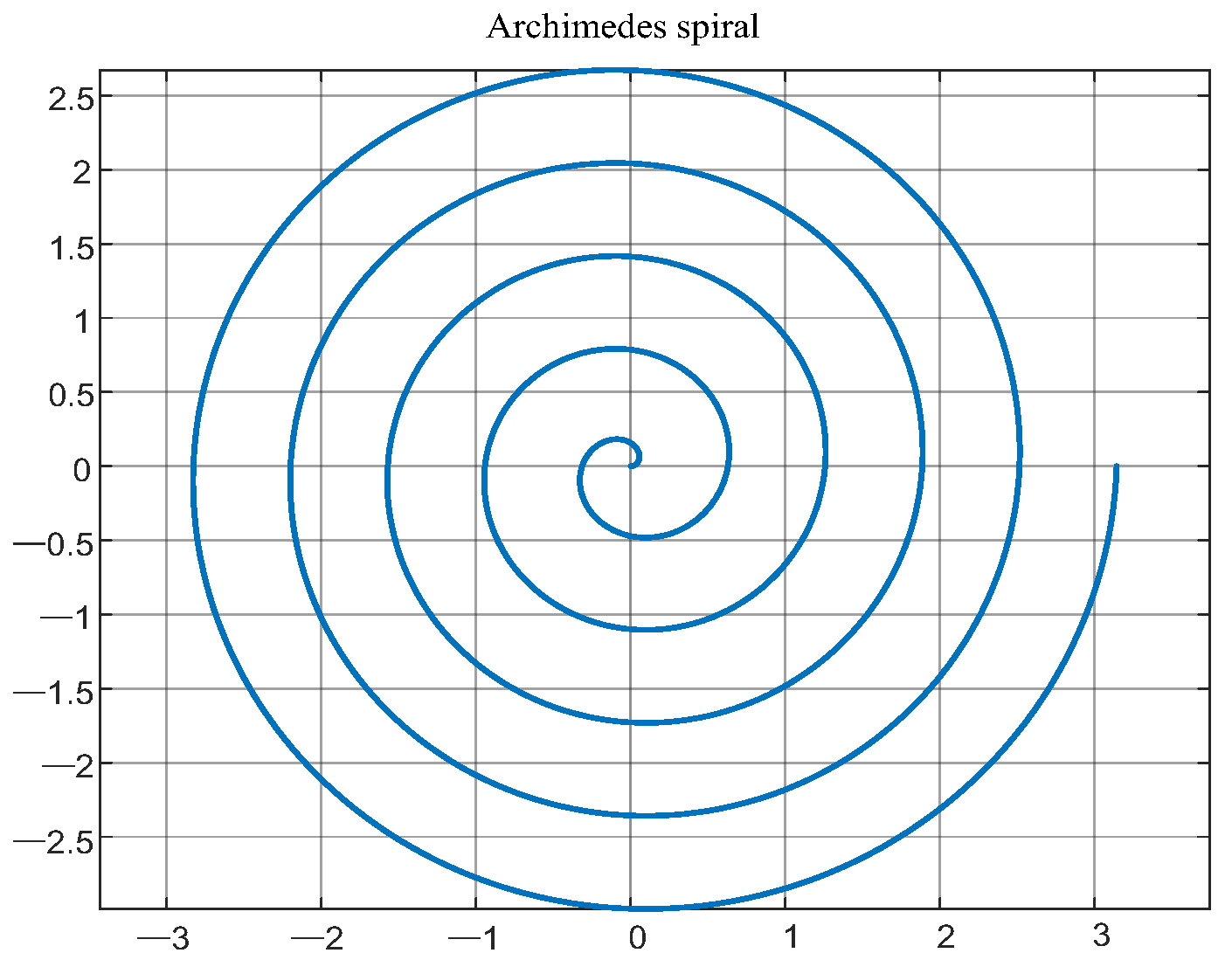
2.3. Basic Principle of Archimedes’ Spiral Optical Waveguide

The geometric expression of Archimedes’ spiral is as follows:
r θ = r 0 + Λ 2 π θ
where r0 represents initial radius of the spiral, Λ is the pitch, and θ is the azimuth. Figure 1 shows five turns of Archimedes’ spiral.
The Archimedes’ spiral structure can extend the optical path in a confined space, effectively reducing the size of optical waveguide devices. By adjusting the parameters of the spiral (such as radius, number of turns, etc.), precise control over the optical path length can be achieved, enabling tunable time delays.
The field distribution of an Archimedes’ spiral optical waveguide can be derived from its geometric characteristics and electromagnetic field theory. In optical waveguide, the light field distribution.is typically obtained by solving Maxwell’s equations. For an Archimedes’ spiral optical waveguide, the field distribution can be expressed as the superposition along the spiral path. Assuming that the electric field distribution in the optical waveguide is E ( τ , θ , z ) , its general form can be expressed as follows:
E ( τ , θ , z ) = E 0 ( r ) e i ( l θ k z )
where l represents the length of Archimedes’ spiral optical waveguide, E 0 r is related to the wavelength of light, while λ is the wavelength of light.
As depicted in Figure 2, the heat distribution in the spiral waveguide is characterized by distinct patterns in both the top and side views. The top view shows the transverse distribution of the thermal field along the spiral path of the waveguide, with high-temperature regions concentrated on the inner side of the curved segments. The side view reveals the vertical distribution of the thermal gradient in the waveguide cross-section, indicating that heat is primarily dissipated toward the cladding.

2.4. Digital Tunable Technology Based on Optical Switch

Digital tunable technology based on optical switch is a technology that manipulates the optical signal path through optical switch mechanisms to achieve the discrete adjustment of optical parameters, including time delay, dispersion, and filtering. Digital tuning of these parameters can be realized by designing selective switching of multiple paths or cascaded switches. This technology offers notable advantages such as discrete control, ease of integration, and straightforward programmability, thereby enabling rapid and accurate optical signal processing and regulation. In this study, a digital tunable true time delay line of optical waveguide based on an Archimedes’ spiral structure is designed. The detailed design methodology and comprehensive simulation outcomes will be elaborated in Section 3, providing in-depth insights into the technical feasibility and performance characteristics of the proposed design.

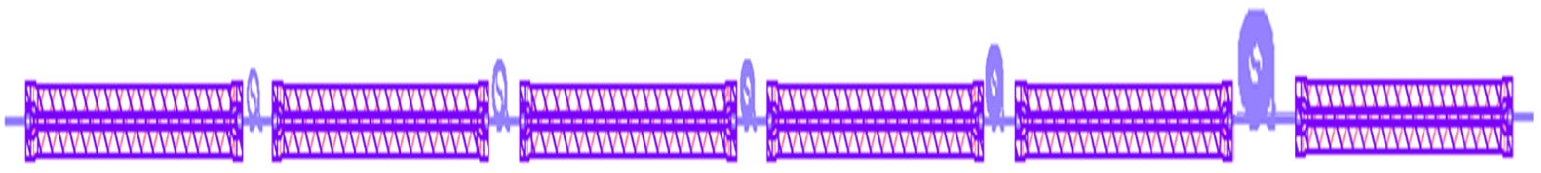
3. Design and Simulation of Optical Waveguide Digital Adjustable Delay Lines Based on Optical Switches and Archimedean Spiral Structures

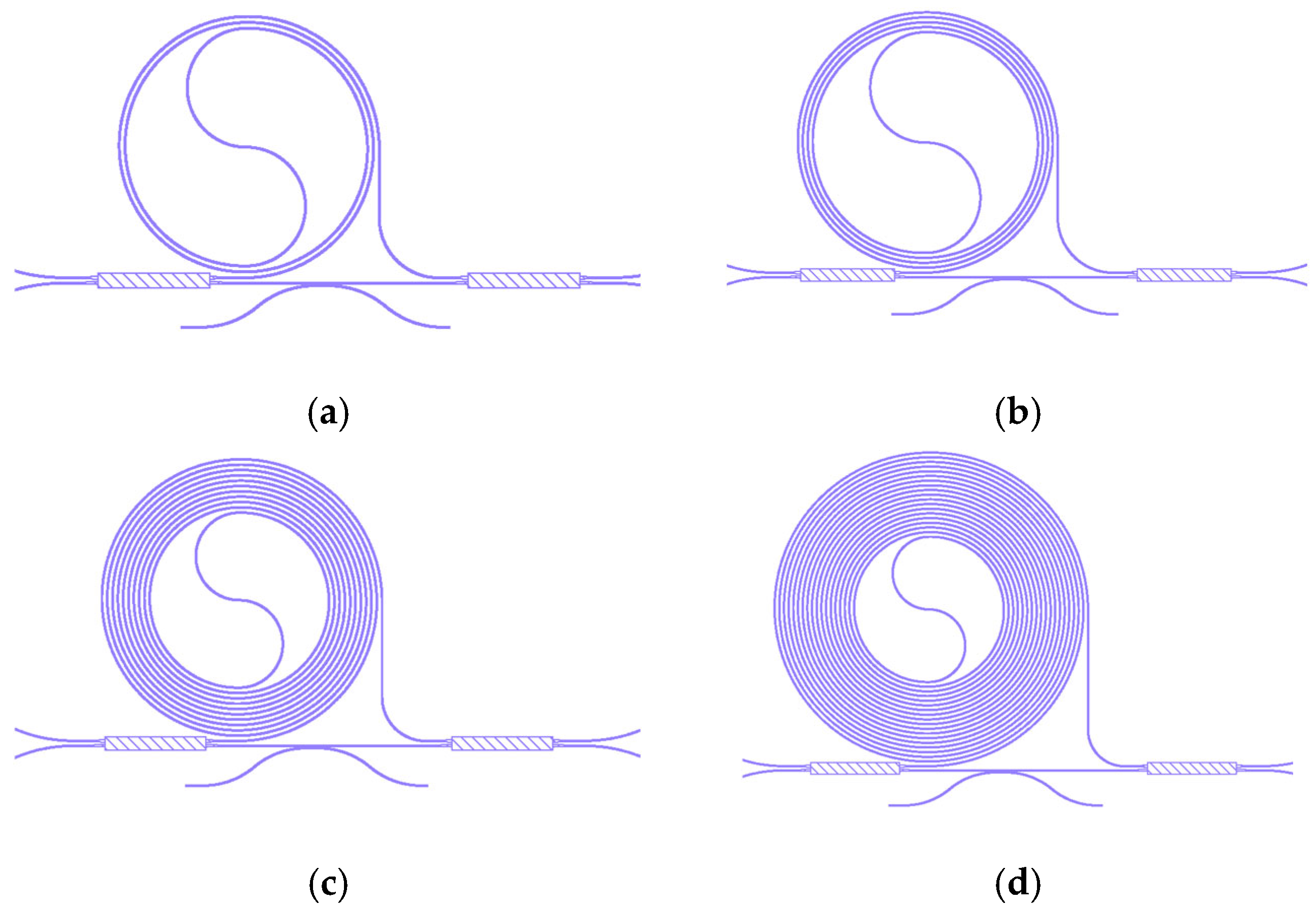
3.1. Design Idea of Optical True Delay Line

In this study, a 2 × 2 Multi-Mode Interference (MMI) coupler, in conjunction with a Mach–Zehnder modulator, is employed to realize on-off selection of the optical path. The upper optical path traverses a silicon nitride waveguide spiral delay line with ultra-low loss characteristics. Specifically, five distinct spiral structures are designed to introduce delays of 10 ps, 20 ps, 40 ps, 80 ps, and 160 ps, respectively, thereby achieving a discrete adjustable delay ranging from 10 to 310 ps in 10 ps increments. Conversely, the lower path is a straight-through configuration, ensuring no additional delay is introduced. By applying voltage to alter the state of the lithium niobate switch, various combinations of these delay values can be realized, which constitutes the fundamental principle of the proposed digital adjustable delay line. Figure 3 illustrates the structural diagram of the digital tunable true delay line.
As depicted in Figure 3, manipulating the switch state enables the combination of various delay values. By altering the state of the switch, it can realize the mutual combination of different delay amounts. Table 1 systematically presents the corresponding relationship between switch state and delay value.
The time delay of the Archimedes’ waveguide spiral follows a pattern where it increases exponentially as the N power of 2. In this study, the designed delays are 10 ps, 20 ps, 40 ps, 80 ps, and 160 ps, respectively. By precisely controlling the through and cross states of the optical switch, this configuration can achieve optical true time delay with a minimum step of 10 ps, covering a range from 10 ps to 310 ps, as comprehensively summarized in Table 1.
Figure 4 shows the design layout of optical true delay lines. The layout features five optical switches integrated with five spiral waveguide delay structures, forming a compact and highly functional configuration. The chip size of the optical true delay line designed in this paper is less than 4 mm × 30 mm.

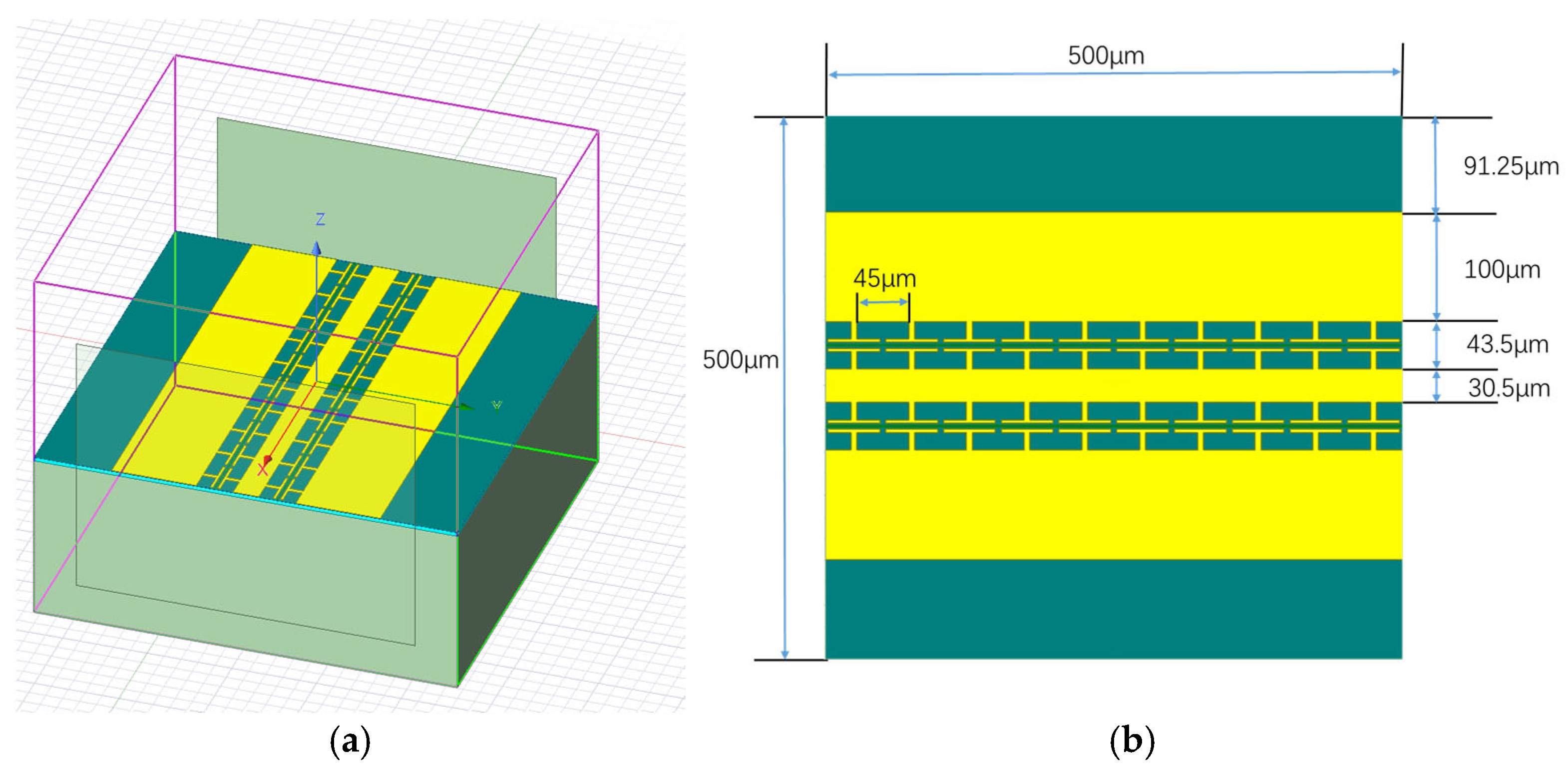
3.2. Specific Design

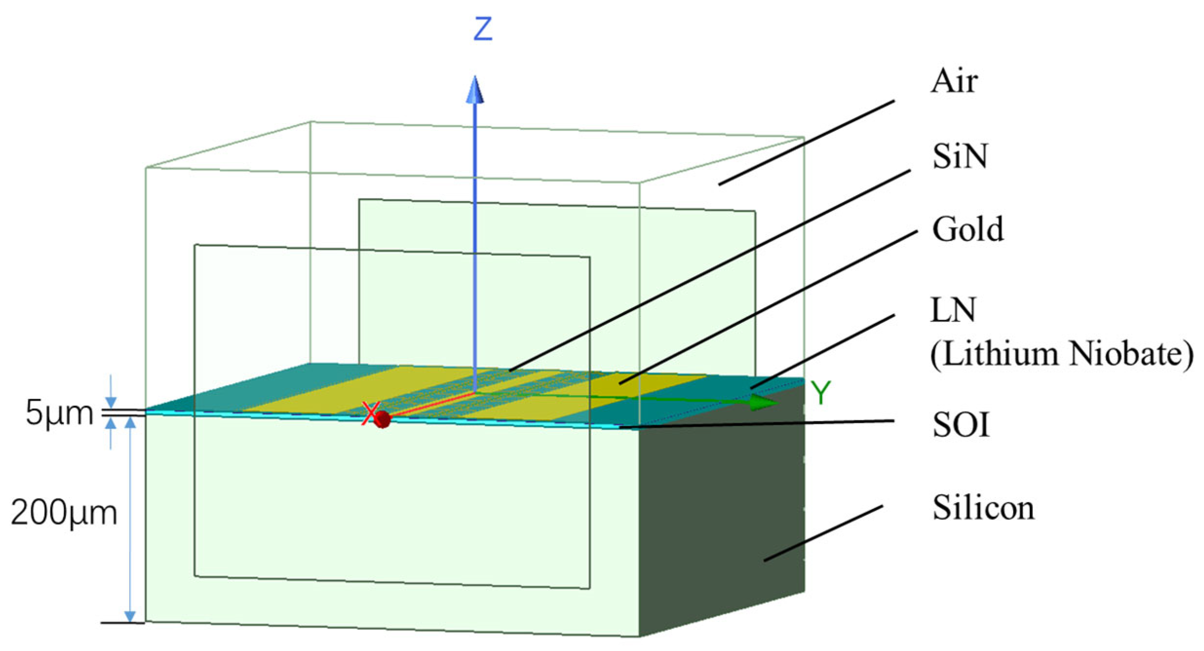
3.2.1. Design of SiN-LiNbO3 Optical Switch

The Mach–Zehnder modulator, in conjunction with a 2 × 2 MMI structure, enables the realization of an optical transmission channel selection switch. An external voltage source applies a voltage to change the phase of the light wave to interfere with it and change the output port of the light wave, so as to realize the selection switch function on the optical transmission channel.
The losses associated with a 2 × 2 MMI typically include transmission losses, mode conversion losses, bending losses, coupling losses, and absorption losses inherent to the material. In this study, the Ansys Lumerical 2024 R1 software, employing the finite-difference time domain (FDTD) method, was utilized for comprehensive analysis. The MMI is equipped with a power monitor placed at the input and output end faces. By directly quantifying the power difference between the input and output, the total loss is directly obtained through α = 10 lg P o u t / P in . Simulation results indicated that the 2 × 2 MMI loss exhibits a total loss of less than 0.75 dB at a wavelength of 1550 nm.
Furthermore, by applying the following formula
P I = P o u t 1 P o u t 2 P o u t 1 + P o u t 2 × 100 %
we obtained the power imbalance of a 2 × 2 MMI, and that is PI = 0.5 dB.
Regarding the optical switch integrated on TFLN material, the Pockels coefficient along its highest principal axis is significantly high. This coefficient is r L i N b O 3 30 33   p m / V , over 300 times that of silicon ( r s i l i c o n 0.1   p m / V ),endowing TFLN with unique electro-optic properties. When an electric field is applied, the refractive index of TFLN changes linearly with the electric field intensity. This linear electro-optic effect occurs without the need for carrier accumulation or nonlinear optical processes, enabling fast responses on the picosecond to nanosecond scale.
As reported in the study by Zhizhang Wang et al. from Nanjing University [50], the response speed of the optical switch can reach 14.4 ns, which is below 20 ns. Such a high-speed response significantly improves the fast-tuning ability of microwave beamforming.
Table 2 presents the structural parameters of the 2 × 2 MMI device. The main body size of MMI features dimensions of 76 μm × 10 μm × 0.5 μm, corresponding to its length, width and height (i.e., thickness), respectively. The width plays a crucial role in determining the number of modes within the multi-mode transmission region. For the silicon nitride waveguide employed in this study, a width of 10 μm enables the support of multiple transverse mode transmission. This characteristic facilitates the formation of a symmetrical output distribution following the interference process.
The length of MMI is primarily governed by the interference effect and generally adheres to the following formula:
L = n e f f W 2 4 λ
where neff is the effective refractive index, W is the waveguide width, and λ is the wavelength. The selected length of 76 μm satisfies the self-imaging condition at the wavelength of 1.55 μm, ensuring that the input light achieves power sharing or specific coupling at the output end. Meanwhile, the thickness of 0.5 μm aligns with the common thin-film silicon nitride processing standard. This parameter effectively balances the constraints of light field confinement and processing feasibility, while minimizing bending-induced optical loss.
A taper structure is employed to connect the standard waveguide and MMI body, minimizing mode mismatch loss through gradual adjustments in width and height. The four-dimensional symmetric design (comprising two pairs of positive/negative y-coordinates) ensures symmetry of input/output ports, thereby eliminating polarization-dependent loss.
The position of the light source is (−13 μm, 1.75 μm, 0 μm), with a size of 3 μm × 2 μm, and the wavelength of the light source is 1.5 μm–1.6 μm. The switch selection function is illustrated in Figure 5. An external voltage source applies an electrical signal to the Mach–Zehnder modulator, inducing a phase change in the light wave propagating through its two arms. This phase alteration leads to interference between the two optical paths within the modulator, ultimately redirecting the light wave to a different output port. By precisely controlling the magnitude and polarity of the applied voltage, the optical signal can be selectively routed, thereby achieving the function of an optical switch that facilitates manipulation of light propagation paths in the designed delay line system. We also obtained the half-wave voltage of the switch, Vπ, which is lower than 3 V.

3.2.2. Archimedes’ Spiral Waveguide Delay Line

The phase change of optical waveguide is related to wavelength, group refractive index, and waveguide length, which satisfies the following formula:
φ ( ω ) = 2 π λ ( ω ) n e f f ( ω ) L
The group delay is shown in Equation (8) below:
T g r o u p = φ ( ω ) ω = L c [ n e f f ( ω ) + ω n e f f ( ω ) ω ] = L c n g r o u p ( ω )
According to simulation, the group refractive index of waveguide delay line is about 2.08. Archimedes’ spiral optical waveguide lithography layout designed in this study is shown in Figure 6.
The spiral waveguide delay line proposed in this study is designed for 1.5 μm–1.6 μm optically controlled beamforming networks, aiming to compensate for the aperture transition time required by each subarray. Constructed as a staggered Archimedes’ spiral delay line, the bending radius is constantly changing. Figure 6 depicts the chip design layout of the spiral waveguide at 1550 nm, taking an 80 ps delay structure as an example. Occupying an area of approximately 0.3 mm × 0.3 mm, the structure is composed of two groups of semicircles, one of which is used to lead the light into the center and the other is used to lead the light out for output. These inward and outward semicircles are connected by an S-shaped structure, and the radius of the structure remains large enough to achieve lossless transmission and mode position stability in the middle of the spiral waveguide. The time delay can be calculated according to the following formula:
t d = n g L c
where td is the time delay of the spiral delay line, ng is the effective index, and c is the speed of light. For the effective group index ng of 1.62 (TE mode) and 1.51 (TM mode), the calculated delay time of the structure at 1550 nm precisely matches the designed value of 80 ps, validating the accuracy of the proposed design and theoretical model.
Table 3 list the structural parameters of spiral waveguide delay line designed in this study.

3.2.3. Design and Simulation of Electrode

The electrode plays a key role in the performance, efficiency, stability and functionality of the device. The layout and material properties of the electrodes directly modulate the electric field distribution within the device. The strength and direction of the electric field can be optimized by reasonably designing the shape, size, and position of the electrode. The electrodes of the optical true delay line designed in this study are shown in Figure 7.
Figure 7 provides a visual representation of their configuration and spatial arrangement. The overall size of the electrode is 500 μm × 500 μm. The purple line defines the spatial boundary, as shown in Figure 7a. The core structure is a two-dimensional waveguide array extending along the X-axis, as shown in Figure 7b. The spacing between two adjacent units in the array is 45 μm.
As is shown in Figure 8, the materials from top to bottom are SiN, Gold, Lithium Niobate, and SOI. The base layer, constructed from Si material, has a thickness of 200 μm. The middle SOI layer, approximately 5 microns thick, serves as a crucial intermediate medium. Notably, the Lithium Niobate layer, with a thickness of 800 nm, plays a key role in the electro-optic modulation process due to its excellent electro-optic properties.

4. Result Analysis

4.1. Analysis of Delay Losses in Different Delay Times

An in-depth analysis of delay lines with varying delay times has been performed, as presented in Table 4. The total loss comprises transmission loss, bending loss, optical switch loss, and coupling loss. Its numerical change reflects the energy attenuation characteristics of the delay line under different delay requirements, and is the key index to evaluate the transmission efficiency of the system. Table 4 meticulously documents 31 sets of data, revealing that the total loss ranges from 2.1345 dB to 6.0398 dB. This range corresponds to the total losses of optical true time delay line systems with delay times ranging from 10 ps to 310 ps.
Experimental observations indicate that total loss demonstrates a linear correlation with the increase in waveguide length and bending frequency. Notably, when the number of bends exceeds 200, the loss growth rate exhibits a marginal acceleration, potentially attributed to enhanced mode leakage caused by the reduction in waveguide bending radius. The loss variation fluctuates within the range of 0.1245 dB–0.1370 dB, with an average increment of about 0.13 dB per 10 ps delay. The incremental fluctuation is attributed to the coupling effect of nonlinearly increasing bending counts and transmission length. As the delay time increases from 10 ps to 310 ps, transmission loss increases from 0.0445 dB to 1.3795 dB, while the bending loss increases from 0.09 dB to 2.66 dB. Collectively, these two factors account for 76.5% of the total loss increment, establishing them as the primary contributors to loss degradation.

4.2. Analysis of the Overall Performance of Digital Dimmable True Delay Line

This study proposes a tunable optical true delay line based on the SiN-LiNbO3 platform, featuring a maximum delay time of 310 ps and a resolution of 10 ps. In recent years, substantial theoretical investigations and experimental validations on multi-path switchable optical switches have been conducted by numerous scholars and research teams, yielding remarkable advancements in the field. A comparative analysis between the proposed work and related studies in the literature is presented in Table 5, highlighting the performance metrics and technical characteristics of different approaches.
The comparative analysis reveals that the delay range, maximum delay tunable range, and loss–delay ratio of optical true time delay lines are significantly influenced by their design structures and fabrication platforms. Notably, in terms of the maximum delay tunable range, the proposed design demonstrates an enhancement of over 60% compared to similar solutions (such as Literature [29]), effectively meeting a wider spectrum of delay adjustment requirements. Literature 38 focuses on long delay amounts; however, its tuning step size, as large as 10,000 ps, severely restricts the system’s ability to perform fine-grained parameter adjustments. When compared with Literature [29] and Literature [42], the proposed method not only outperforms in terms of the delay range but also exhibits a lower loss delay ratio, underscoring its superiority in achieving a better balance between delay performance and loss characteristics.

5. Conclusions

This study presents a tunable optical true delay line constructed on the SiN-LiNbO3 platform, boasting a maximum delay time of 310 ps and a resolution of 10 ps. Benefiting from the linear electro-optic effect of TFLN, the response speed of the optical switch can be less than 20 ns. This remarkable performance significantly enhances the rapid tuning capabilities of microwave beamforming systems, enabling more agile and precise control over signal delays.
The proposed optical true delay line exhibits a distinct advantage in its low delay–loss ratio, a key performance metric indicating minimal signal attenuation per unit delay. This characteristic not only ensures efficient energy utilization within the device but also underscores its potential for high-fidelity signal transmission. As a core component in optoelectronics system, the low-loss and rapid-switching OTTD is expected to attract significant attention in strategic applications such as optical communications and microwave photonic radar systems. For future research directions, efforts will be concentrated on further reducing transmission losses by exploring advanced low-loss waveguide materials and optimizing waveguide bending structures.

Author Contributions

L.L. conceived the original idea and designed the research framework; T.A. and G.L. put forward the true time delay methodology; C.H. conducted simulations of spiral waveguides and verified the rationality of structures; Y.M. and Y.N. conducted formal analysis; S.Z. and Y.J. performed data curation; T.A. completed the initial draft writing; T.A. secured the research funding through Youth Independent Innovation Research Foundation. All authors have read and agreed to the published version of the manuscript.

Funding

This research was funded by Youth Independent Innovation Research Foundation, grant number KYSZJKQTZQ23013.

Institutional Review Board Statement

Not applicable.

Informed Consent Statement

Not applicable.

Data Availability Statement

The original contributions presented in this study are included in the article. Further inquiries can be directed to the corresponding author.

Acknowledgments

The authors have reviewed and edited the output and take full responsibility for the content of this publication.

Conflicts of Interest

The authors declare no conflicts of interest.

References

  1. Wang, Y.; Dong, Z.; Ding, J.; Li, W.; Wang, M.; Zhao, F.; Yu, J. Photonics-assisted joint high-speed communication and high resolution radar detection system. Opt. Lett. 2021, 46, 6103–6106. [Google Scholar] [CrossRef] [PubMed]
  2. Shi, S.; Niu, H.; Shi, W.; Lin, D.; Li, S.; Pan, S.; Yun, B. Integrated Optical Tunable Delay Line and Microwave Photonic Beamforming Chip: A Review. Laser Photonics Rev. 2024, 19, 202400663. [Google Scholar] [CrossRef]
  3. Capmany, J.; Novak, D. Microwave photonics combines two worlds. Nat. Photonics 2007, 1, 319–330. [Google Scholar] [CrossRef]
  4. Zhang, M.Y. Optically Controlled Phased Array Radar; National Defense Industry Press: Beijing, China, 2008; pp. 1–4. [Google Scholar]
  5. Pan, S.L.; Zhang, Y.M. Microwave Photon radar and key technologies. Sci. Technol. Rev. 2017, 35, 36–52. [Google Scholar]
  6. Pan, S.L.; Zhang, Y.M. Microwave Photonic Radar. J. Light. Technol. 2020, 38, 5450–5484. [Google Scholar] [CrossRef]
  7. Sun, H.B.; Li, S.L.; Wang, Q.; Li, X.K. Development of phased array radar antenna delay technology. J. Microw. 2021, 37, 9–15. [Google Scholar]
  8. Hu, C.; Luo, B.; Bai, W.L.; Pan, W.; Yan, L.; Zou, X. Stable radio frequency transmission of single optical source over fiber based on passive hase compensation. IEEE Photonics J. 2021, 13, 7200607. [Google Scholar] [CrossRef]
  9. Lenz, G.; Eggleton, B.J.; Madsen, C.K.; Slusher, R.E. Optical delay lines based on optical filters. IEEE J. Quantum Electron. 2001, 37, 525–532. [Google Scholar] [CrossRef]
  10. Liang, H.; Wang, K.; Han, S.; Mei, L.; Tian, Z.; Zhang, J.; Chong, M. Research on Delay and Bandwidth Expansion of Discrete Dispersive Fourier Transform in the Optical Domain. Semicond. Optoelectron. 2024, 45, 1–7. [Google Scholar]
  11. Wang, H.; Chen, L.; Qi, Y.; Ba, D.; Dong, Y. Ultrafast microwave photonics frequency measurement technology. Laser Optoelectron. Prog. 2024, 61, 0112003. [Google Scholar]
  12. Subha Priyadharshini, C.; Rajeswari, A. High-Capacity Optical Communication Systems using 4D Spatial-Wavelength-Zero Cross Correlation Encoding. IETE J. Res. 2025, 1, 1–13. [Google Scholar] [CrossRef]
  13. Yessenov, M.; Bhaduri, B.; Delfyett, P.J.; Abouraddy, A.F. Free-space optical delay line using space-time wave packets. Nat. Commun. 2020, 11, 5782. [Google Scholar] [CrossRef]
  14. Wu, Y.L.; Bao, W.S.; Cao, S.R.; Chen, F.; Chen, M.-C.; Chen, X.; Chung, T.-H.; Deng, H.; Du, Y. Strong quantum computational advantage using a superconducting quantum processor. Phys. Rev. Lett. 2021, 127, 180501. [Google Scholar] [CrossRef]
  15. Jurcevic, P.; Jacadi-Abhari, A.; Bishop, L.S.; Lauer, I.; Bogorin, D.F.; Brink, M. Demonstration of quantum volume 64 on a superconducting quantum computing system. Quantum Sci. Technol. 2021, 6, 025020. [Google Scholar] [CrossRef]
  16. Bliek, L.; Wahls, S.; Visscher, I.; Taddei, C.; Timens, R.B.; Oldenbeuving, R.M.; Roeloffzen, C.G.H.; Verhaegen, M. Automatic Delay Tuning of a Novel Ring Resonator-Based Photonic Beamformer for a Transmit Phased Array Antenna. J. Light. Technol. 2019, 37, 346–348. [Google Scholar] [CrossRef]
  17. Xiang, C.; Davenport, M.L.; Khurgin, J.B.; Morton, P.A.; Bowers, J.E. Low-Loss continuously tunable optical true time delay based on Si3N4 ring resonators. IEEE J. Sel. Top. Quantum Electron. 2018, 24, 1–9. [Google Scholar] [CrossRef]
  18. Shan, W.; Lu, L.; Wang, X.; Zhou, G.; Liu, Y.; Chen, J.; Zhou, L. Broadband continuously tunable microwave photonic delay line based on cascaded silicon microrings. Opt. Express 2021, 29, 3375. [Google Scholar] [CrossRef] [PubMed]
  19. Xue, X.X.; Xuan, Y.; Bao, C.Y.; Li, S.; Zheng, X.; Zhou, B. Microcomb-based true-time delay network for microwave beamforming with arbitrary beam pattern control. J. Light. Technol. 2018, 36, 2312–2321. [Google Scholar] [CrossRef]
  20. Sun, H.; Wang, Y.; Chen, L.R. Integrated discretely tunable optical delay line based on step-chirped subwavelength grating waveguide bragg gratings. J. Light. Technol. 2020, 38, 5551–5560. [Google Scholar] [CrossRef]
  21. Srivastava, N.K.; Parihar, R.; Raghuwanshi, S.K. Efficient photonic beamforming system incorporating a unique featured tunable chirped fiber Bragg grating for application extended to the ku-band. IEEE Trans. Microw. Theory Tech. 2020, 68, 1851–1857. [Google Scholar] [CrossRef]
  22. Perez-lopez, D.; Sanchez, E.; Capmany, J. Programmable true time delay lines using integrated waveguide meshes. J. Light. Technol. 2018, 36, 4591–4601. [Google Scholar] [CrossRef]
  23. Zhu, C.; Lu, L.; Shan, W.; Xu, W.; Zhou, G.; Zhou, L.; Chen, J. Silicon integrated microwave photonic beamformer. Optica 2020, 7, 1162. [Google Scholar] [CrossRef]
  24. Sun, X.H. True Time-Delay Optical Beamforming Technology with Optic Switched Differential Structure and its Application in Radar Target Direction Finding. Master’s Thesis, Zhejiang University, Hangzhou, China, 2022; pp. 41–48. [Google Scholar]
  25. Duan, X.; Zhang, S.T.; Jiang, Y.Y. Improvement and implementation of a multi-channel programmable optical controlled true time delay network. Opt. Commun. Technol. 2017, 41, 1–4. [Google Scholar]
  26. Niu, X.Y.; Gu, Y.R.; Chu, X.; Yao, J.; Yao, J.; Yi, M.; Wang, L. Primary study on time control technology of active phasedarray based on photoconductive microwave source. High Power Laser Partical Beams 2023, 36, 1–6. [Google Scholar]
  27. Tessema, N.M.; Cao, Z.; Zantvoort, J.H.C.V.; Mekonnen, K.A.; Trinidad, A.M.; Tangdiongga, E.; Smolders, A.B.; Koonen, A.M.J. Wavelength-dependent Continuous Delay Based on a Si3N4 Optical Ring Resonator for K-band Radio Beamformer. In Proceedings of the IEEE International Topical Meeting on Microwave Photonics, California, CA, USA, 31 October–3 November 2016; IEEE: Piscataway, NJ, USA, 2016; pp. 305–308. [Google Scholar]
  28. Xie, J.; Zhou, L.; Li, Z.; Wang, J.; Chen, J. Seven-bit reconfigurable optical true time delay line based on silicon integration: Erratum. Opt. Express 2014, 22, 25516. [Google Scholar] [CrossRef]
  29. Zheng, P.F.; Wang, C.Q.; Xu, X.M.; Li, J.; Lin, D.D.; Hu, G.H. A Seven Bit Silicon Optical True Time Delay Line for Ka-Band Phased Array Antenna. IEEE Photonics J. 2019, 11, 1–9. [Google Scholar] [CrossRef]
  30. Zheng, P.F.; Xu, X.M.; Lin, D.D.; Liu, P.C.; Hu, G.H.; Yun, B.F. A wideband 1 × 4 optical beam-forming chip based on switchable optical delay lines for Ka-band phased array. Opt. Commun. 2021, 488, 126842. [Google Scholar] [CrossRef]
  31. Zhang, L.; Hong, S.H.; Wang, Y.; Yan, H.; Xie, Y.; Chen, T.; Zhang, M.; Yu, Z.; Shi, Y.; Liu, L.; et al. Ultralow-Loss Silicon Photonics beyond the Singlemode Regime. Laser Photonics Rev. 2022, 16, 2100292. [Google Scholar] [CrossRef]
  32. Shi, S.Q.; Hu, G.H.; Lin, D.D.; Zhang, J.Y.; Liu, P.C.; Lu, M.J.; Cheng, W.; Lin, T.; Yun, B.F.; Cui, Y.P. Performance comparison of integrated optical switching delay lines on three typical photonic integration pilot lines. Opt. Laser Technol. 2023, 159, 109016. [Google Scholar] [CrossRef]
  33. Xie, Y.W.; Hong, S.H.; Yan, H.; Zhang, C.P.; Zhang, L.; Zhuang, L.M.; Dai, D.X. Low-loss chip-scale programmable silicon photonic processor. Opto-Electron. Adv. 2023, 6, 220030. [Google Scholar] [CrossRef]
  34. Fathpour, S.; Riza, N. Silicon-photonics-based wideband radar beamforming: Basic design, Optical. Engineering 2010, 49, 018201. [Google Scholar] [CrossRef]
  35. Moreira, R.L.; Garcia, J.; Li, W.; Bauters, J.; Barton, J.S.; Heck, M.J.R.; Bowers, J.E.; Blumenthal, D.J. Integrated Ultra-Low-Loss 4-Bit Tunable Delay for Broadband Phased Array Antenna Applications. IEEE Photonics Technol. Lett. 2013, 25, 1165–1168. [Google Scholar] [CrossRef]
  36. Lin, D.; Shi, S.; Liu, P.; Cheng, W.; Lu, M.; Lin, T.; Hu, G.; Yun, B.; Cui, Y. Low loss silicon nitride 1 × 4 microwave photonic beamforming chip. Opt. Express 2022, 30, 30672–30683. [Google Scholar] [CrossRef]
  37. Song, Q.Q.; Hu, Z.F.; Chen, K.X. Scalable and reconfigurable true time delay line based on an ultra-low-loss silica waveguide. Appl. Opt. 2018, 57, 4434–4439. [Google Scholar] [CrossRef] [PubMed]
  38. Liu, D.P.; Sun, S.Q.; Yin, X.; Sun, B.; Sun, J.; Liu, Y.; Li, W.; Zhu, N.; Li, M. Large-capacity and low-loss integrated optical buffer. Opt. Express 2019, 27, 11585–11593. [Google Scholar] [CrossRef]
  39. Howley, B.; Wang, X.; Chen, M.; Chen, R.T. Reconfigurable Delay Time Polymer Planar Lightwave Circuit for an X-band Phased-Array Antenna Demonstration. J. Light. Technol. 2007, 25, 883–890. [Google Scholar] [CrossRef]
  40. Wang, X.L.; Howley, B.; Chen, M.Y.; Chen, R.T. Phase error corrected 4-bit true time delay module using a cascaded 2 × 2 polymer waveguide switch array. Appl. Opt. 2007, 46, 379–383. [Google Scholar] [CrossRef]
  41. Pan, Z.; Subbaraman, H.; Lin, X.; Li, Q.; Zhang, C.; Ling, T.; Guo, L.J.; Chen, R.T. Laser Science to Photonic Applications. In Proceedings of the Conference on Lasers and Electro-Optics (CLEO), San Jose, CA, USA, 8–13 June 2014. [Google Scholar]
  42. Ke, W.; Lin, Y.; He, M.; Xu, M.; Zhang, J.; Lin, Z.; Yu, S.; Cai, X. Digitally tunable optical delay line based on thin-film lithium niobate featuring high switching speed and low optical loss. Photonics Res. 2022, 10, 2575–2583. [Google Scholar] [CrossRef]
  43. Chen, R.T. Polymer-based photonic integrated circuits. Opt. Laser Technol. 1993, 25, 347–365. [Google Scholar] [CrossRef]
  44. Hong, S.; Zhang, L.; Wu, J.; Peng, Y.; Lyu, L.; Hu, Y.; Xie, Y.; Dai, D. Multimode-enabled silicon photonic delay lines: Break the delay-density limit. Light Sci. Appl. 2025, 14, 145. [Google Scholar] [CrossRef]
  45. Wang, X.; Zhou, L.; Li, R.; Xie, J.; Lu, L.; Wu, K.; Chen, J. Continuously tunable ultra-thin silicon waveguide optical delay line. Optica 2017, 4, 507–515. [Google Scholar] [CrossRef]
  46. Hong, S.H.; Zhang, L.; Wang, Y.; Zhang, M.; Xie, Y.; Dai, D. Ultralow-loss compact silicon photonic waveguide spirals and delay lines. Photonics Res. 2022, 10, 1–7. [Google Scholar] [CrossRef]
  47. Ma, T.; Ma, M.; Guo, L.J. Optical multilayer thin film structure inverse design: From optimization to deep learning. iScience 2025, 28, 112222. [Google Scholar] [CrossRef]
  48. Trager, F. Modern Optics and Photonics Technology; Springer: Berlin/Heidelberg, Germany, 2012. [Google Scholar]
  49. Liu, S.; Li, C. Photonics Technology and Application; Guangdong Science and Technology Press: Guangzhou, China, 2006. [Google Scholar]
  50. Wang, Z.Z.; Li, X.Y.; Ji, J.T.; Sun, Z.; Sun, J.; Fang, B.; Lu, J.; Li, S.; Ma, X.; Chen, X.; et al. Fast-speed and low-power-consumption optical phased array based on lithium niobate waveguides. Nanophotonics 2024, 13, 2429–2436. [Google Scholar] [CrossRef]
Figure 1. Archimedes’ spiral structure (5 turns).
Photonics 12 00679 g001
Figure 2. The heat distribution in the spiral waveguide: (a) top view; (b) side view.
Photonics 12 00679 g002
Figure 3. Digital adjustable true delay line. (a) Structure diagram. (b) ”Through” switch state. (c) “Cross” switch state. (d) Switch unit. (e) Delay line unit.
Photonics 12 00679 g003
Figure 4. Design layout of optical true delay lines.
Photonics 12 00679 g004
Figure 5. Distribution of switch selection function field: (a) the phase of the lower arm is 90° (b) the phase of the upper arm is 90°.
Photonics 12 00679 g005
Figure 6. Archimedes’ spiral waveguide delay line: (a) 10 ps delay, (b) 20 ps delay, (c) 40 ps delay, and (d) 80 ps delay.
Photonics 12 00679 g006
Figure 7. Schematic diagram of electrode: (a) schematic diagram of the three-dimensional structure of the electrode; (b) schematic diagram of xoy cross-sectional structure.
Photonics 12 00679 g007
Figure 8. The material of the electrode and the thickness of various materials.
Photonics 12 00679 g008
Table 1. Corresponding relationship between switch state and delay value.
Switch 1Switch 2Switch 3Switch 4Switch 5Delay Value
throughcrossthroughthroughthrough10 ps
crosscrosscrossthroughthrough20 ps
throughthroughcrossthroughthrough30 ps
crossthroughcrosscrossthrough40 ps
throughcrosscrosscrossthrough50 ps
crosscrossthroughcrossthrough60 ps
throughthroughthroughcrossthrough70 ps
crossthroughthroughcrosscross80 ps
throughcrossthroughcrosscross90 ps
crosscrosscrosscrosscross100 ps
throughthroughcrosscrosscross110 ps
crossthroughcrossthroughcross120 ps
throughcrosscrossthroughcross130 ps
crosscrossthroughthroughcross140 ps
throughthroughthroughthroughcross150 ps
crossthroughthroughthroughcross160 ps
throughcrossthroughthroughcross170 ps
crosscrosscrossthroughcross180 ps
crossthroughcrosscrosscross190 ps
crossthroughcrosscrosscross200 ps
throughcrosscrosscrosscross210 ps
crosscrossthroughcrosscross220 ps
throughthroughthroughcrosscross230 ps
crossthroughthroughcrossthrough240 ps
throughcrossthroughcrosscross250 ps
crosscrosscrosscrossthrough260 ps
throughthroughcrosscrossthrough270 ps
crossthroughcrossthroughthrough280 ps
throughcrosscrossthroughthrough290 ps
crosscrossthroughthroughthrough300 ps
throughthroughthroughthroughthrough310 ps
Table 2. Structural parameters of 2 × 2 MMI in this paper.
ComponentDimensions/PositionThicknessType
MMI76 μm × 10 μm × 0.5 μm/(10 μm × 1 μm × 0.5 μm)0.5 μmRectangle
Input waveguide_up10 μm × 1 μm × 0.5 μm/(−15 μm, −1.75 μm, 0.15 μm)0.5 μmRectangle
Input waveguide_down10 μm × 1 μm × 0.5 μm/(−15 μm, −1.75 μm, 0.15 μm)0.5 μmRectangle
Output waveguide_up10 μm × 1 μm × 0.5 μm/(91 μm, 1.75 μm, 0.15 μm)0.5 μmRectangle
Output waveguide_down10 μm × 1 μm × 0.5 μm/(91 μm, −1.75 μm, 0.15 μm)0.5 μmRectangle
Taper 1(0 μm, 1.75 μm, 0.15 μm)0.5 μmPolygon
Taper 2(0 μm, −1.75 μm, 0.15 μm)0.5 μmPolygon
Taper 3(0 μm, 1.75 μm, 0.15 μm)0.5 μmPolygon
Taper 4(0 μm, −1.75 μm, 0.15 μm)0.5 μmPolygon
Table 3. Structural parameters of spiral waveguide delay line designed in this paper.
MaterialRadius of CurvatureWaveguide Spacing
Silicon nitrideSpiral center: R0 = 88.6 μmReverse waveguide spacing 4 μm
Outside the center: R(θ) = 88.6 + 0.637θ (μm)Co-directional waveguide spacing 4 μm
Table 4. The delay losses in different delay times.
Delay Time
[ps]
Waveguide Length
[cm]
Transmission Loss
[dB]
Bending TimesBending Loss
[dB]
Optical Switch Loss
[dB]
Coupling Loss
[dB]
Total Loss
[dB]
100.0890.044590.09112.1345
200.1780.0890170.17112.2590
300.2670.1335260.26112.3935
400.3560.1780340.34112.5180
500.4450.2225430.43112.6550
600.5340.2670510.51112.7770
700.6230.3115600.60112.9115
800.7120.3560690.69113.0460
900.8010.4005780.78113.1805
1000.8900.4450860.86113.3050
1100.9790.4895950.95113.4395
1201.0680.53401031.03113.5640
1301.1570.57851121.12113.6985
1401.2460.62301201.20113.8230
1501.3350.66751291.29113.9575
1601.4240.71201371.37114.0820
1701.5130.75651461.46114.2165
1801.6020.80101541.54114.3410
1901.6910.84551631.63114.4755
2001.7800.89001711.71114.6000
2101.8690.93451801.80114.7345
2201.9580.97901881.88114.8590
2302.0471.02351971.97114.9935
2402.1361.06802062.06115.1280
2502.2251.11252152.15115.2625
2602.3141.15702232.23115.3870
2702.4031.20152322.32115.5215
2802.4921.24602402.40115.6460
2902.5811.29052492.49115.7805
3002.6701.33502572.57115.9050
3102.7591.37952662.66116.0398
Table 5. Performance comparison of tunable delay lines based on multi-path switchable optical switches.
LiteraturePlatformDelay Tuning Step
[ps]
Maximum Delay Tunable Range
[ps]
Loss Delay Ratio
[dB ns−1]
Footprint
[mm2]
[29]SOI1.52191.3717.8113.32
[36]Si3N44.21301.835
[37]SiO2690.25.5602
[38]SiO210,000100,0000.224166
[42]TFLN101502350
This workSiN-LiNbO31031013120
Disclaimer/Publisher’s Note: The statements, opinions and data contained in all publications are solely those of the individual author(s) and contributor(s) and not of MDPI and/or the editor(s). MDPI and/or the editor(s) disclaim responsibility for any injury to people or property resulting from any ideas, methods, instructions or products referred to in the content.

