1. Introduction
The capacity demand in communication networks has grown exponentially, driven by the proliferation of emerging technological advancements, including the Internet of Things, massive machine-type communications, and artificial intelligence [
1,
2]. Coherent optical communication technology is widely deployed across critical infrastructure domains, including data center interconnects, metro area networks, and bone networks [
3]. Coherent optical communication technology enables the encoding of information across multiple physical dimensions of light, such as polarization (PDM [
4], DP-DQPSK [
5]) and phase (high-order constellation modulation [
6,
7]), which can significantly enhance data transmission rates. The 90° optical hybrid is a core component in coherent optical communication systems, where it combines the incoming coherent modulated optical signal with the local oscillator signal to enable balanced detection and IQ demodulation [
8]. The common-mode rejection ratio (CMRR) and phase error represent the two most critical performance metrics for evaluating 90° optical hybrids, as they directly impact the bit error rate (BER) of coherent receivers in optical communication systems.
Waveguide-based 90° optical hybrids have become the focus of extensive research owing to their advantageous characteristics, including their compact size and compatibility with photonic integrated circuit (PIC) technology. A 90° optical hybrid coupler based on an MMI coupler, composed of single-mode input/output waveguides and a slab multimode waveguide, demonstrates superior characteristics, including structural simplicity, a broad operational bandwidth, and minimal insertion losses. Reports have shown the successful implementation of 90° optical hybrids on different integrated platforms, including plasmons [
9], indium phosphate [
10], silicon-on-insulator [
11], silicon nitride [
12], and so on. Recently, thin-film lithium niobate (TFLN) has attracted significant research attention due to its advantageous properties, including its large refractive index contrast, wide transparency window, and high nonlinear efficiency, gradually emerging as a promising integrated photonic platform [
13,
14]. So far, 90° optical hybrids have been successfully demonstrated on the TFLN platform, including a design based on a 4 × 4 MMI coupler [
15] and a wedge-shaped configuration utilizing tapered 2 × 4 and 2 × 2 multimode interference (MMI) couplers [
16]. Nevertheless, the former design suffers from a relatively large chip area, necessitating further size reduction, whereas the latter introduces structural complexity that increases fabrication difficulties.
In this work, a 90° optical hybrid with an MMI coupler on x-cut TFLN was designed and tested. It was fabricated on a 600 nm thick x-cut TFLN substrate with a partial etch depth of 300 nm. The fabricated 90° optical hybrid exhibited a CMRR larger than 20 dB, a phase error below ±7.5°, and an excess loss less than 1.8 dB (including contributions from the 90° hybrid, the 1 × 2 MMI coupler, and the optical delay line, after subtracting the losses from the coupler and delay line, the 90° optical hybrid introduced less than 0.9 dB of loss) over the C-band with a compact footprint of 13.8 × 250 μm2, demonstrating outstanding performance with an ultra-compact size and a simple design.
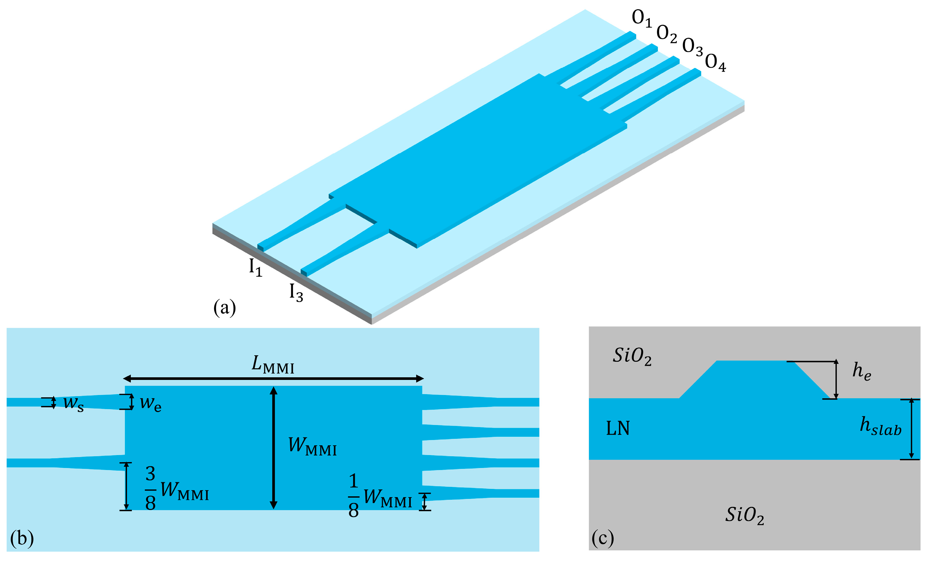
2. Device Design
As depicted in
Figure 1, the proposed 90° optical hybrid, based on an MMI coupler, was fabricated on a 600 nm thick x-cut TFLN substrate with the following partial etch depth: he = 300 nm. The modulated signal and the local oscillator light (LO) were simultaneously injected into input ports 1 and 3 of the 90° optical hybrid. The electric fields at the four output ports (
O1–
O4) after interference within the MMI coupler are represented below [
17]:
where
ES and
ELO are two input complex fields of the signal and LO, and
φs,i and
φLO,i (i = 1, 2, 3, 4) represent the phase shift from input ports 1 or 3 (corresponding to the launched signal or LO light, respectively) to the output ports. Then, the relative phase differences of the four output channels can be represented as follows: ∆
φs,i =
φs,i −
φLO,i. The output electric fields
Eout,1 and
Eout,4 correspond to the in-phase (I) signal, and
Eout,2 and
Eout,3 correspond to the quadrature (Q) signal. Generally, two pairs of balanced detectors are connected to the in-phase (I) signal and quadrature (Q) signal to detect the phase in a QPSK system.
Here, we briefly explain the basic theory related to self-imaging in the MMI region [
18]. Basically, in order to ensure the proper operation of the 90° optical hybrid, the beat length
Lπ should satisfy the following condition
where
β0 and
β1 denote the propagation constant of the fundamental mode and the first-order mode, respectively. Because of the strong lateral confinement provided by the ridge waveguide structure, the optical field is tightly confined, and
Lπ can be approximated as follows:
where
nr and
λ0 indicate the refractive index and wavelength, respectively.
We stands for the effective MMI width. The theoretical length of the MMI coupler (
LMMI) is defined by the following equation:
Based on Equation (4), we can ascertain that the length of the MMI coupler (
LMMI) is related to
WMMI and
nr. To ensure high-quality imaging, the MMI must demonstrate low phase errors for the higher-order modes. Additionally, sufficient space between the input and output ports is necessary to minimize mutual crosstalk. By comprehensively considering factors such as loss, phase error, and size, we set the width of the MMI to
WMMI = 13.8 µm, with a corresponding length of
LMMI = 250 µm. The widths of the input and output ports were optimized to
We = 2.5 µm based on the method described in [
19] and linearly tapered to
Ws = 1 µm using adiabatic tapers with a length of 25 µm to minimize mode mismatch losses at the junctions. Owing to the sufficient separation between the ports, crosstalk at the output ports was found to be negligible.
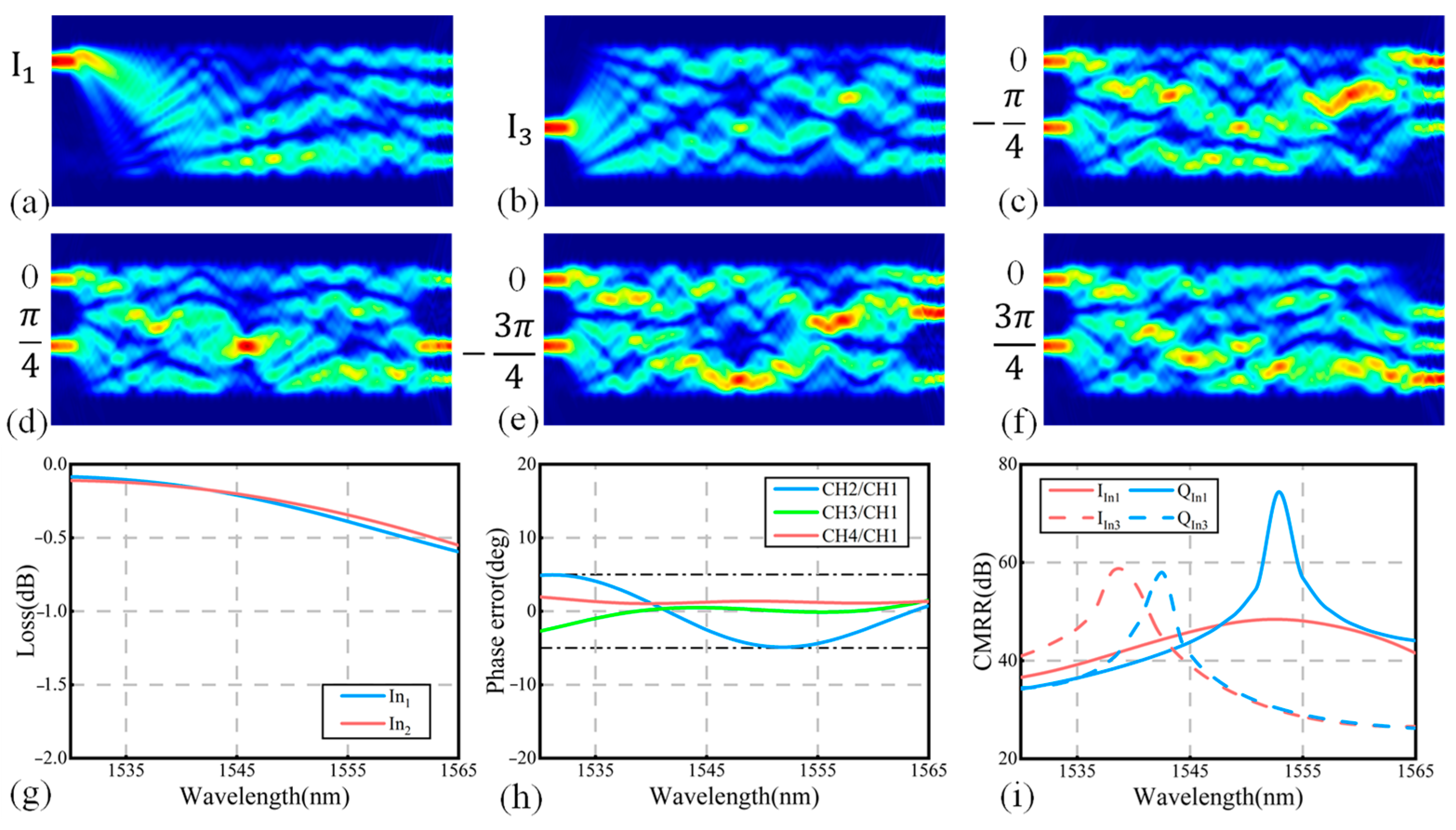
The electrical field distributions of the MMI coupler at 1550 nm were calculated using the finite-difference time-domain (FDTD) method, with TE-mode light being incident from
I1 and
I3, respectively, as shown in
Figure 2a,b. From the profiles, the four output optical fields demonstrate equal intensity levels.
Figure 2c–f show the electrical field distributions under different initial phase conditions for two input fields, i.e., (0, −π/4), (0, π/4), (0, −3π/4), and (0, 3π/4), proving that this design can effectively function as a 90° optical hybrid. To further evaluate the performance of the 90° optical hybrid, the wavelength dependence of the excess loss, phase errors, and CMRRs were analyzed using 3D FDTD simulations over a broad spectral range from 1530 nm to 1565 nm. In
Figure 2g, the excess loss is below 0.6 dB across the wavelength span of 1530 to 1565 nm. Phase error serves as a critical performance metric in a 90° optical hybrid, directly impacting the reliability of balanced detection. As shown in
Figure 2h, the output phase deviations remain within ±5° across the wavelength range of 1530 nm to 1565 nm. Additionally, the common mode rejection ratios (CMRR) represent the output power balance of the I/Q channel [
20]. In
Figure 2i, the CMRRs exceed 20 dB across the entire C-band, indicating a good power balance between the in-phase and quadrature channels.
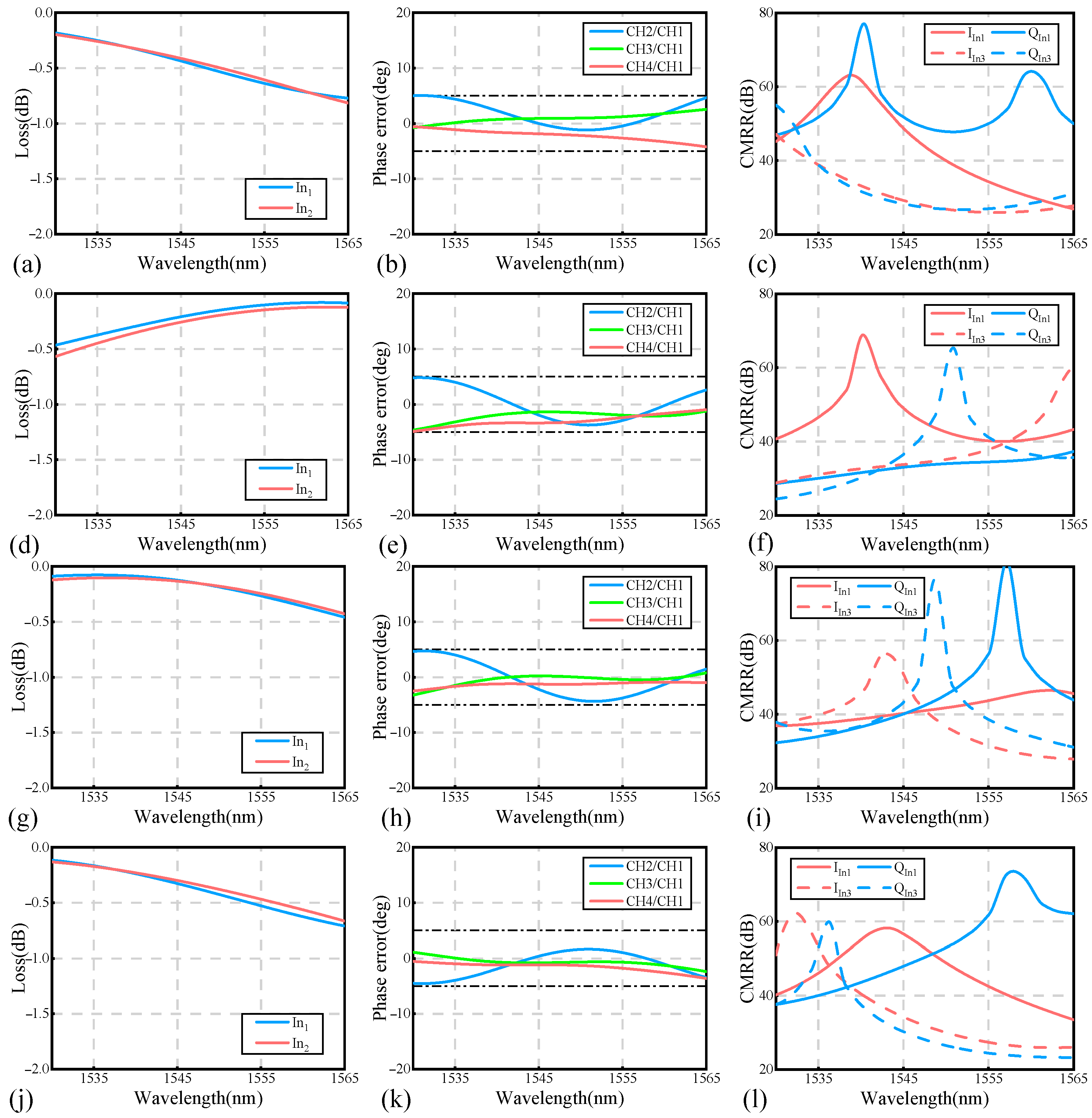
The impact of MMI fabrication tolerances on the performance of the proposed 90° optical hybrid was investigated. As shown in
Figure 3a–f, the performance metrics were as follows: excess loss < 0.6 dB, phase error < 5°, and CMRR > 20 dB over a wavelength range from 1535 to 1565 nm when
WMMI in 13.8 µm ± 0.1 µm. Furthermore, the performance of the MMI with different lengths was also investigated. An excess loss < 0.8 dB, a phase error < 5°, and a CMRR > 20 dB across the whole C-band could still be achieved despite a fabrication length deviation of ∆
L = ±1 µm, as shown in
Figure 3g–l. These results confirm that the proposed 90° optical hybrid exhibits excellent tolerance to fabrication variations.
3. Experimental Results
The proposed 90° optical hybrid was fabricated on an x-cut TFLN wafer. A high-quality LN substrate was subjected to high-dose He
+ (or H
+) ion implantation to define a cleavage plane at the target film thickness. Meanwhile, a handle wafer—typically LN or silicon with an oxide layer—was prepared. After bonding the LN substrate to the handle wafer, thermal annealing was used to initiate layer splitting along the cleavage plane, resulting in the formation of the thin film [
13]. The TFLN consists of a 600 nm thick top LN layer, a 4.7 μm thick silicon dioxide (SiO
2) layer, and a 500 μm thick silicon substrate. The structure was defined utilizing an electron beam lithography (EBL) system, followed by the etching of a 300 nm thick lithium niobate (LN) layer through inductively coupled plasma reactive ion etching (ICP-RIE) technology. Then, a 1000 nm thick silicon dioxide (SiO
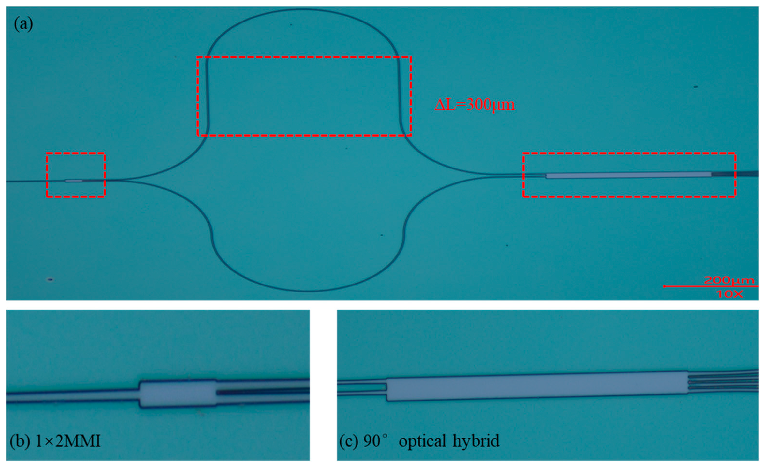
2) upper cladding layer was deposited via plasma-enhanced chemical vapor deposition (PECVD), followed by wafer dicing and precision mechanical polishing to complete the chip-manufacturing process. Scanning electron microscopy (SEM) characterization verified that the fabricated device had dimensions of 13.82 × 250.5 μm
2. In the previous Section, we conducted simulation analyses on the fabrication tolerances of the chip dimensions, and the results indicated that the device maintained good performance within a width variation of ±0.1 µm and a length variation of ±1 µm. Dimensional measurements of the fabricated chip confirmed that its actual size fell within these specified tolerance ranges. The fabricated structures of the 90° optical hybrid and the 1 × 2 MMI coupler, as observed using microscopy, are shown in
Figure 4.
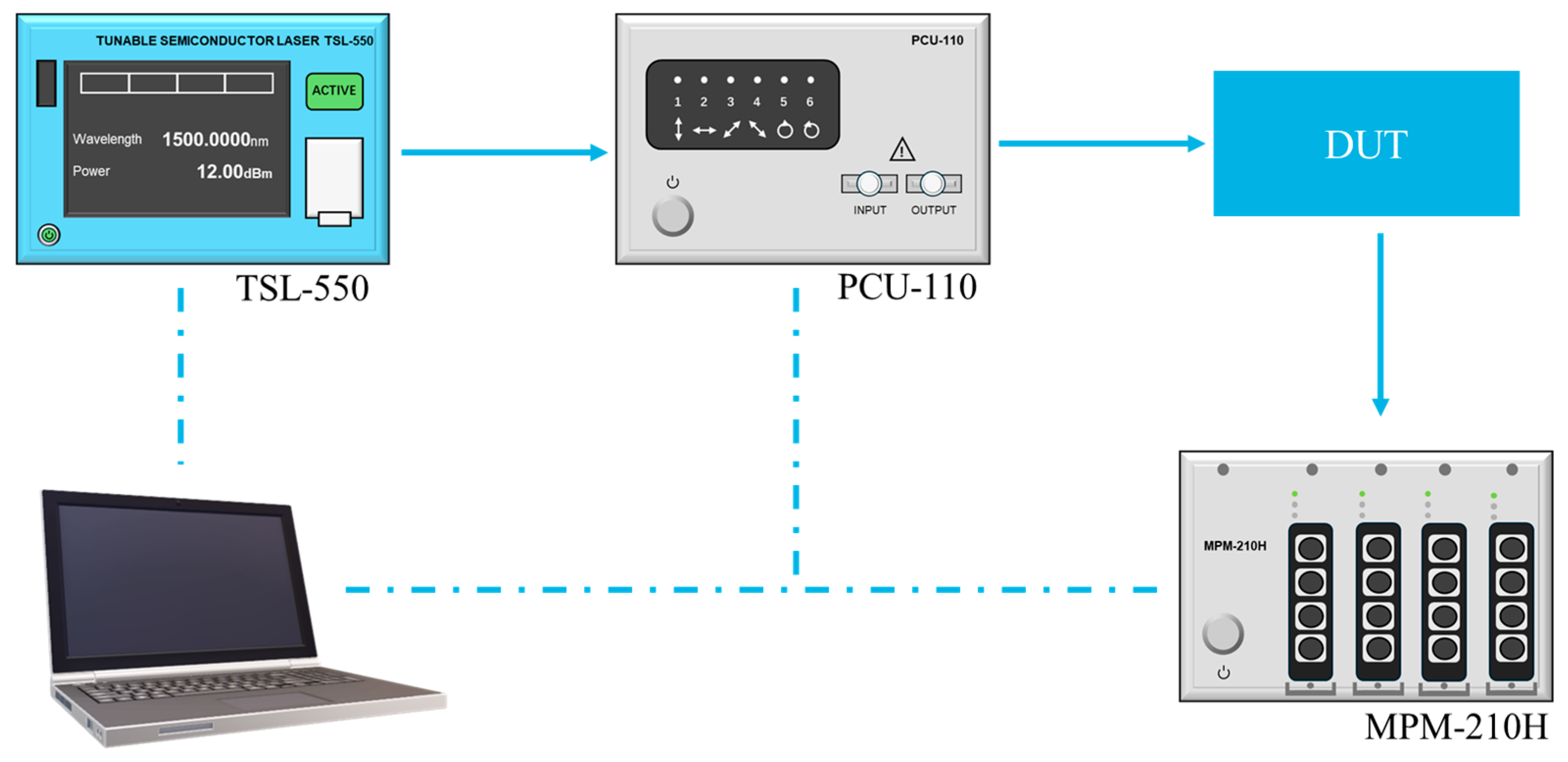
Figure 5 is a schematic of the experimental setup, including the optical hybrid device under testing (DUT) and associated characterization instrumentation. The experimental setup includes a tunable laser source (Santec TSL-550, Santec Holdings Corporation, Komaki, Aichi Prefecture, Japan), a polarization state generation device (Santec PCU-100, Santec Holdings Corporation, Komaki, Aichi Prefecture, Japan), an optical power meter (Santec MPM-210H, Santec Holdings Corporation, Komaki, Aichi Prefecture, Japan), and a lensed fiber with a 3 µm spot size. The tunable laser source operates within a wavelength range of 1520–1580 nm. The device employs end-face coupling as its optical interfacing scheme. The lensed fibers were precisely aligned with the input and output waveguide by using an optical coupling platform. A computer-controlled synchronous scanning system, integrating a tunable laser source, a polarization state generation device, and an optical power meter, enabled automated acquisition of the transmission spectra of the device under testing (DUT) through an optical power meter. The output light from the tunable laser source was coupled with the polarization state generator (Santec PCU-100) via an optical fiber. This device is capable of generating various polarization states on the Poincare sphere, including TE polarization states, TM polarization states, and right-hand circular (RCP) and left-hand circular (LCP) polarization states, relative to the axis defined by an internal linear polarizer. Therefore, the transmission spectra under multiple polarization states can be obtained using an optical power meter. Since the fabricated device operates in a TE polarization state, the required test data can be acquired by selecting the transmission spectrum under the TE polarization state in the control software.
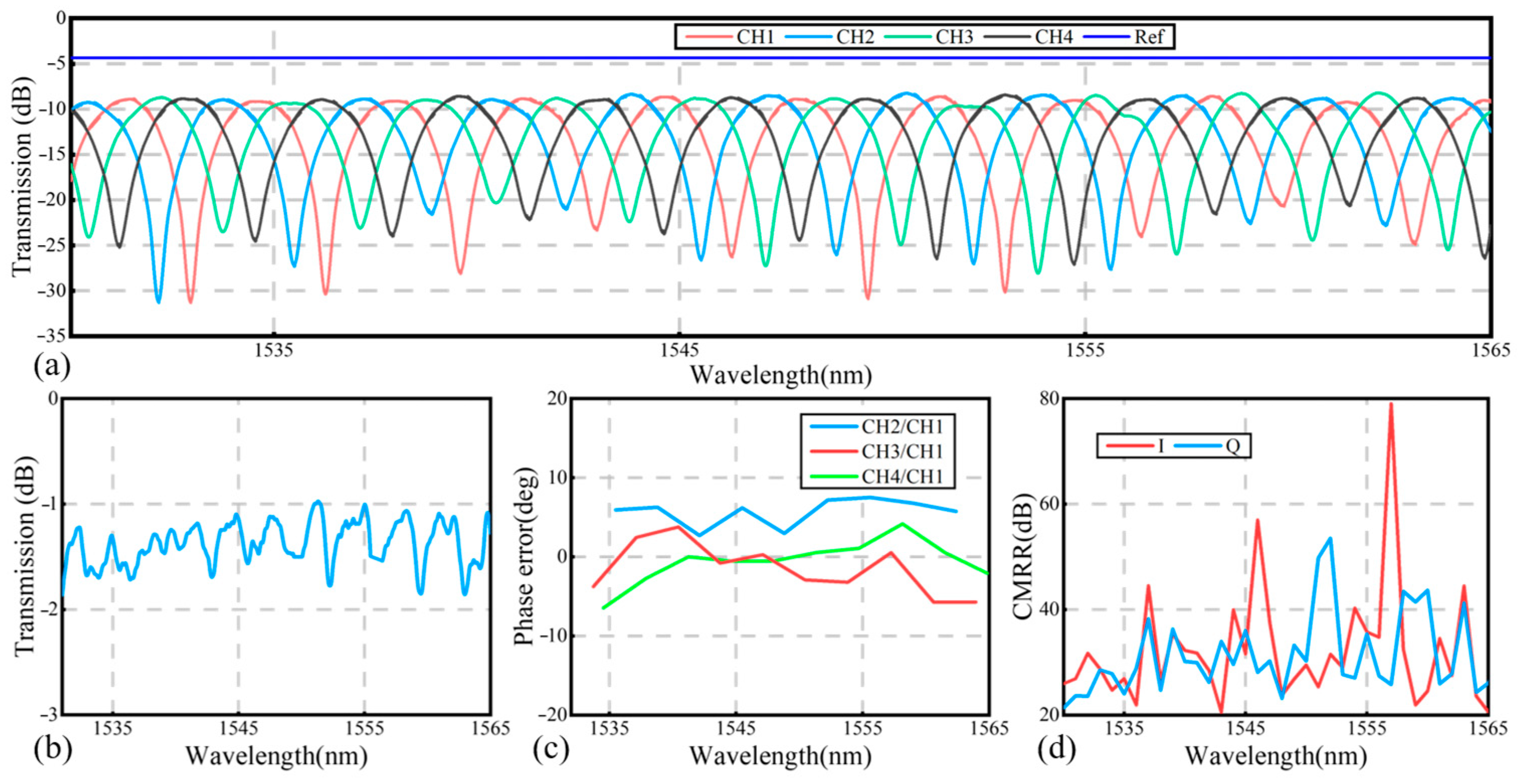
Figure 6a shows the transmission spectra of each port over a wavelength range of 1530–1565 nm. A neighboring straight waveguide with the same width (1 µm) served as a reference waveguide. First, at each fixed wavelength, the output power (in mW) of each output port was extracted from the transmission spectra and summed. The total power was then converted into dBm. Then, at the same wavelength, the excess loss of the chip was obtained by subtracting the sum of the output values from the four ports of the 90° optical hybrid from the output value of the reference waveguide.
Figure 6b shows that the excess loss, including contributions from the 90° hybrid, the 1 × 2 MMI coupler, and the optical delay line, remained below 1.8 dB across the C-band. The measured waveguide loss for this setup was 0.8 dB/cm. After the losses were subtracted from the input/output long waveguides, the optical delay line, and the 1 × 2 MMI coupler, the excess loss of the 90°optical hybrid was found to be less than 0.9 dB.
To verify the phase characteristics of the 90° optical hybrid, a Mach–Zehnder interferometer (MZI) was fabricated, consisting of a cascaded 1 × 2 MMI coupler and an optical delay line, as shown in
Figure 4a. Owing to the wavelength-dependent phase shifts introduced by the delay line, the phase information at the output ports of the 90° optical hybrid could be converted into intensity variations for detection.
The laser input was evenly split into two arms via the 1 × 2 MMI coupler. Upon passing through the delay line and reaching input Ports 1 and 3, the two beams developed a constant phase difference. By varying the incident wavelength, one can tune this phase difference accordingly. Consequently, the phase shift can be determined through spectral analysis of output power variations at all four ports as a function of the incident wavelength, as expressed by the following formula: Δ
ϕ1,j = 2
πΔλ
1,j/FSR. The spectral minimum wavelength separation (Δλ
1,j) between output ports j and 1 correlates with their corresponding phase deviation Δ
ϕ1,j. The free spectral range (FSR) is defined as the wavelength spacing between adjacent spectral minima in the transmission spectrum of Channel 1. Computational analysis revealed that the phase error of the device was less than ±7.5°, as shown in
Figure 6c. The CMRR for both in-phase (I: P
1/P
4) and quadrature (Q: P
2/P
3) channel pairs was calculated using the following formula: −20 log [(
Pi −
Pj)/(
Pi +
Pj)], where
Pi,j denotes optical power measured at output ports i and j, respectively. The CMRR characterization of the fabricated 90° hybrid’s in-phase (I) and quadrature (Q) channels was carried out using the spectral peak of the output ports. As shown in
Figure 6d, the CMRR of the I/Q channels exceeded 20 dB across the entire C-band.
4. Discussion
With the advancement of semiconductor micro/nanofabrication technologies, planar waveguide optics will continue to provide novel approaches for 90° optical hybrid development. In such waveguide structures, light is confined within micron-scale cores, which enables a substantial reduction in the chip footprint of a 90° optical hybrid.
The current commercially available 90° optical hybrid devices, while demonstrating superior detection accuracy in practical applications, are hindered by three primary limitations: non-compact physical dimensions, incompatibility with integrated coherent transceivers, and high production costs. The proposed 90° optical hybrid based on a multimode interference (MMI) structure addresses these limitations by exhibiting low excess loss, a broad operational bandwidth, and the ability to be created via simple fabrication processes while also demonstrating strong compatibility with integrated coherent receivers.
The performance metrics in
Table 1 contrast the proposed device with existing counterparts across different platforms. Benchmarked against prior 90° optical hybrids with diverse architectures on distinct material platforms, the proposed 90° hybrid demonstrates a more compact footprint while achieving broad operational bandwidth alongside comparable CMRR and excess loss characteristics. The proposed chip structure is manufactured via a simple fabrication process. Further refinement of etching processes presents a viable pathway to reducing excess loss and mitigating phase deviations in 90° optical hybrids, potentially enhancing device performance metrics. This 90° optical hybrid has promising prospects for integration with high-speed photodetectors and coherent modulators to realize a compact, heterogeneously integrated coherent transceiver.

 ,
, 
