Abstract
The 2 μm wavelength is ideal for light detection and ranging and gas sensing due to its eye-safe operation, strong molecular absorption targeting, and low atmospheric scattering—critical for environmental monitoring and free-space communications. The existing 2 μm systems rely on mechanical beam steering, which limits speed and reliability. Integrated photonic solutions have not yet been demonstrated in this wavelength. We propose a focal plane array design to address these challenges. Compared to optical phased arrays requiring complex phase control for each antenna, FPAs have a simple switch-based control and high suppression of background noise. Although FPAs need an external lens for beam collimation, they significantly reduce system complexity. This study introduces a compact, low-loss 1 × 8 focal plane array operating in the 2 μm range, employing a cascaded Mach–Zehnder interferometer switch array on a silicon nitride platform. The device demonstrates a field of view of 16.8°, background suppression better than 17 dB, and excess loss of −1.4 dB. This integrated photonic beam steering solution offers a highly promising, cost-effective approach for rapid beam switching. This integrated photonic beam steering solution offers a highly promising, cost-effective approach for rapid beam switching.
1. Introduction
The 2 µm spectral region has emerged as a transformative platform for photonic systems, offering distinct advantages compared with conventional wavelengths, including broad gain bandwidth in thulium-doped amplifiers [1], excellent atmospheric transmission with enhanced eye safety [2] and its position within the atmospheric window of weak absorption [3]. These characteristics make it particularly suitable for free-space optical communications, atmospheric monitoring and Light Detection and Ranging (LiDAR) applications [4], where its spectral alignment with key gas absorption features enables precise environmental sensing [5,6,7,8,9]. Coherent Doppler LiDAR systems leverage this wavelength for wind measurement [4] and differential absorption LiDAR utilizes it for greenhouse gas detection [6,9]. Beam steering is a critical technology in LiDAR systems as it enables precise targeting of the light beam. However, these LiDARs utilizing the wavelength of 2 μm have relied on mechanical components such as rotating mirrors and gimbals, for beam steering. While these mechanical solutions can cover a wide scanning range, they are limited in terms of steering speed, cost, size, and reliability [10]. In recent years, on-chip optical beam steering has emerged as a key research area, owing to its compact size and low cost [11,12,13,14]. Among the various solutions, optical phased arrays (OPAs) and focal plane arrays (FPAs) are two common architectures [15,16,17,18,19,20,21,22,23,24,25,26]. While integrated OPAs have been reported to offer a wide field of view (FOV), they require a significant number of optical antennas and fine phase control for each antenna, making the system design significantly more complex [15,16,19,20,21]. In contrast, FPAs consist of an on-chip cascaded switch array, emitters, and an off-chip lens. The switch array is controlled to direct incident light to the selected emitter, which then directs the light into space. The beam is collimated and steered by the off-chip lens. This configuration enables a compact structure with the advantages of simplified control and improved sidelobe and background suppression [17,18,22,23,24,25,26]. While various FPA architectures have been explored for integrated beam steering, fundamental trade-offs persist among control precision, power efficiency, and scalability. The directional coupler-based FPAs [26] leverage compact splitting networks, yet their fixed power splitting ratios limit dynamic control over emitter arrays. Micro-ring resonator arrays [24], though promising for wavelength-routed steering, suffer from thermal crosstalk and stringent fabrication demands. In contrast, cascaded Mach–Zehnder interferometer (MZI) networks [22,23,25] uniquely combine electrically reconfigurable beamforming with thermally isolated phase control, enabling precise phase calibration across large-scale arrays. Among various integrated photonic platforms, silicon-on insulator (SOI) and silicon nitride-on-insulator (SNOI) photonic integrated circuits (PICs) offer distinct advantages for on-chip laser beam steering. These platforms benefit from a high refractive index contrast and CMOS-compatible fabrication processes, resulting in compact, cost-effective devices [27]. Compared to SOI, SNOI features a broader transparent window across the visible to mid infrared spectrum [28,29,30], enabling lower transmission losses when applied to 2 μm on-chip optical beam steering. Extensive research has been conducted on on-chip optical beam steering in the 1.55 μm wavelength band using SOI and SNOI platforms [18,19,20,22,24]. To the best of our knowledge, there is no report on on-chip optical beam steering systems operating in the 2 μm wavelength band yet. In this work, we demonstrate a compact and low-loss integrated 1 × 8 FPA operating in the 2 μm wavelength range, utilizing a MZI cascaded switch array. Fabricated on a silicon–nitride platform, the device achieves an impressive FOV of 16.8°, background suppression of 17–26 dB, and an excess loss of approximately −1.4 dB.
2. Design and Methods
A schematic of the silicon nitride-based FPA device is shown in Figure 1a. The device consists of an on-chip 1 × 8 MZI thermal switch array and an end-fire emitter array. The light source at the wavelength of 2 μm is coupled into the chip by a standard lensed fiber. The silicon–nitride waveguide was designed with a size of 2.2 μm × 0.3 μm to support the TE/TM mode. The 1 × 8 MZI switch array is designed as a binary tree structure, comprising cascaded 2 × 2 MZI thermal switches. Applying electric power (p > 0, Switch on) to an MZI thermal switch generates heat, enabling precise incident light at a wavelength of 2 μm switching between the two output ports (port1 or port2) through optical interference [31,32], as illustrated in diagrams (i) and (ii). The emitter array consists of eight end-fire emitters. An off-chip lens is located on the chip facet, with its focal plane overlapping the plane of the emitter array.
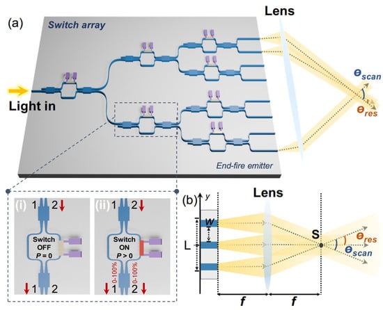
Figure 1.
(a) Schematic illustration of the FPA system. Bottom left inset: a single 2 × 2 MZI thermal switch that routes light between two ports: (i) when no power is applied (p = 0), light exits through port2 (port1); (ii) as power increases (p > 0), light smoothly transitions between the output ports, ranging from 0% to 100%, until it is fully directed to port2 (port1). (b) Schematic showing the working principle of the FPA.
The incident light is guided to a single emitter through the binary control at each MZI in the switch array and then emitted into free space. The beam is subsequently collimated, and its direction is steered by passing through an off-chip lens, as shown in Figure 1b. Beam steering is accomplished by switching the light to different emitters. Multi-point emission is achieved by distributing optical power across multiple emitters through the application of specific electrical power to the MZI switch array. The emission angle can be calculated as:
Here, f and y represent the focal length of the lens and the coordinate of the selected emitter relative to the optical axis of the lens (y = 0), respectively. The optical beam steering to different angles in the far-field is achieved by activating emitters at various positions. The field of view (θscan) and angular resolution (θres) are defined as:
where w is the array pitch, f is the focal length of the lens, and n is the number of optical emitters.
3. Chip Fabrication
The device was fabricated on a SNOI wafer with a 300 nm thick device layer and a 4.4 µm thick buried oxide layer. To define the device structures, electron-beam lithography (EBL) with ARP 6200 resist was used, followed by reactive ion etching (RIE) for pattern transfer. A 2.9 µm SiO2 layer was deposited using inductively coupled plasma chemical vapor deposition (ICP-CVD) and the sample was planarized and thinned to 2.4 µm with IC1-200 dielectric material. A dry etching process was then applied for optical and electrical optimization. A 200 nm thick titanium (Ti) layer and a 10 nm thick gold (Au) layer were deposited by electron beam evaporation to form the heater for thermal phase tuning, followed by the deposition of a 300 nm thick Au layer for the formation of contact wires and pads. The chip, sized at 12 mm × 1 mm, is mounted on a copper substrate with PCBs wire-bonded to the on-chip electrodes to supply power from a voltage source, as shown in Figure 2a,d. A microscope image of the fabricated device is shown in Figure 2e. As shown in Figure 2b, the FPA device integrates two key components: a switch array and a facet emitter array. The switch array comprises seven MZI thermal switches, each incorporating two 2 × 2 MMIs and a phase shifter. As detailed in Figure 2a, the phase shifter has a length of 1 mm.
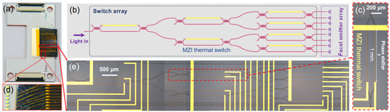
Figure 2.
(a) Picture of the bonded FPA device. (b) Schematic illustration of the FPA device. (c) Detailed microscopic image of the MZI thermal switch. (d) Detailed microscopic image of the gold bonding wire. (e) Microscopic image of the fabricated FPA device.
4. Chip Characterization
Light is coupled into the silicon nitride chip from lensed fibers through edge couplers, with a 2 μm wavelength laser (Newport TLB-6736) serving as the light source. The TE polarization is stabilized using a polarization controller, and two 6-axis mechanical alignment stages are employed to precisely adjust the coupling between the lensed fiber and the device. The output port is similarly coupled to a lensed fiber through edge couplers, with a photodetector used to assess the device’s performance.
The width of the single-mode waveguide is 2.2 µm. The propagation loss at 2 μm wavelength was characterized by measuring spiral waveguides with varying lengths (2.35 cm, 4.15 cm, 5.95 cm, and 7.85 cm). As shown in Figure 3a, the experimental data were fitted to yield a propagation loss of 1.07 dB/cm, where the x-axis and y-axis represent the waveguide length and corresponding optical loss, respectively. To calibrate the excess loss of the device, the transmission loss of a straight waveguide on the same chip was used for comparison.
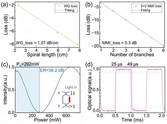
Figure 3.
(a) The loss of the single-mode waveguide. (b) The loss of the single 2 × 2 MMI. (c) Normalized optical output power measured through output Port2 of the single MZI switch. The inset shows the light output from Port2 when a power of Pπ is applied. (d) Response time measurement of the single MZI switch.
The single thermally tunable MZI consists of two 2 × 2 MMIs and two waveguide arms, with the multimode interference region of each 2 × 2 MMI measuring 110 × 14 µm2. Figure 3b presents the excess loss measurement of six cascaded 2 × 2 MMIs, where linear fitting reveals a per-MMI excess loss of 0.3 dB. The x- and y-axes correspond to the number of cascaded stages and the measured optical loss, respectively. It is important to note that a 2 × 2 MMI inherently introduces a 3 dB loss, a result of the self-imaging principle.
The interference properties of a single MZI switch were characterized using voltage-controlled phase shifters. The phase shifter is 1000 µm in length, which is optimized to improve heat dissipation. Figure 3c shows the power consumption of the single MZI switch, which was measured to be 292 mW for a π-phase shift. At this power level (Pπ = 292 mW), the light at the wavelength of 2 μm is fully emitted from port2, resulting in an extinction ratio of approximately 36.2 dB. The excess loss of the single MZI switch is approximately 0.47 dB. Due to the lower efficiency of thermo-optic tuning at longer wavelengths, as described by FOM∝1/λ3 [33,34,35], more power is required for phase shifting at the wavelength of 2 μm. In this context, FOM refers to the thermo-optic figure of merit.
The modulation speed of the device was evaluated by applying a square wave to the micro-heater, and the output signal was monitored from one port of the MZI using an oscilloscope. To determine the time constants for the rising and falling edges of the signals, the 10–90% transition regions were fitted to an exponential function. The measured switching times for the phase shifter were 25 µs for the rising edge and 49 µs for the falling edge, as shown in Figure 3d.
The phase shifters were adjusted at each stage to facilitate light propagation from port1 to port8. Figure 4a shows the half-wave power of each phase shifter, ranging from 262 mW to 306 mW. The half-wave power of each phase shifter was individually measured to serve as the reference value for precise phase control. The light was fully directed to only one output port under the precise phase control, while the optical intensity of the other output ports was simultaneously measured using lensed fibers and photodetectors. As shown in Figure 4b, the excess losses of the device were greater than or equal to −1.4 dB at each port, while the losses at other ports in the same stage ranged from −20 dB to −36.6 dB. The device exhibited an extinction ratio of approximately 19 dB, which was attributed to the spectral ratio of the 2 × 2 MMI. The excess losses showed a fluctuation of less than 0.5 dB, primarily due to metal absorption losses on the chip surface.
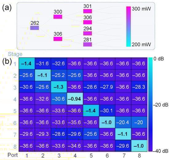
Figure 4.
(a) Half-wave power consumption of MZI thermal switch array. (b) Excess losses of the device, as well as those at each output port, were measured under the precise phase control.
The near-field patterns were observed by placing a lens group and an infrared camera (Pyrocam III, Spiricon, Jerusalem, Israel) behind the emitter array. The lens group consists of an infinity-corrected objective lens (Plan Apo 10x, Nikon, Tokyo, Japan) and a tube lens (f = 200 mm), which expands the patterns emitted from the chip as shown in Figure 5a. The distances between the chip and objective lens, and the objective lens and infrared camera are clearly labeled in Figure 5a. The purpose of expanding the patterns is to match the resolution of the infrared camera’s pixels. The infrared camera features an 80 μm pixel pitch and 12.8 × 12.8 mm2 active area, achieving 64 nW/pixel (CW) and 0.5 nJ/pixel (pulsed) sensitivity.
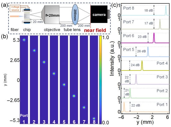
Figure 5.
(a) Measurement setup for near-field. (b) Near-field patterns by emitter selection. (c) Near-field light intensity distribution from port8 to port1 with background suppression ranging from 17 dB to 26 dB.
Figure 5b shows the reconfigurable near-field light patterns. The near-field light patterns have a total length of 10.6 mm, with a pitch of 0.88 mm between adjacent patterns. These patterns, ranging from port1 to port8, were generated by applying different power configurations to the phase shifters of the MZI switch array. Only one output port emits light at a time, while the other ports remain in a state with no light emission. It is clearly observed that all patterns exhibit a clean background, indicating that leakage light from non-operating emitters is negligible. The background suppression of port8 and port7 was measured at 17 dB and 18 dB, respectively, with the suppression in other ports exceeding 20 dB, as shown in Figure 5c.
During near-field testing, errors in light intensity measurements may occur due to the limitations in camera sensitivity and the finite pixel resolution occupied by each pattern. Theoretically, the background suppression ratio is primarily determined by the extinction ratio of the MZI switch, which is superior to that of the OPA beam scanner.
To observe the far-field beam steering, a Fourier lens with a focal length of 35 mm was placed behind the near-field plane, as shown in Figure 6a. After the Fourier transform process, the far-field patterns were emitted from the emitter array. However, due to the limited field of view of the infrared camera, the far-field patterns could not be captured in a single shot. To overcome this limitation, we introduced an imaging lens (focal length matching the FT lens) after the FT lens, forming a 4f imaging system that projects the pattern onto the infrared camera. The system verification was performed by comparing the observed spot patterns (Figure 6b) with the near-field image. The excellent agreement between them (spot spacing ≈ 0.88 mm) confirms the accuracy of our optical alignment. Based on this confirmation, the scanning angle of 16.8° and resolution of 1.43° (derived from the spot spacing and focal length) represents the actual measured value.
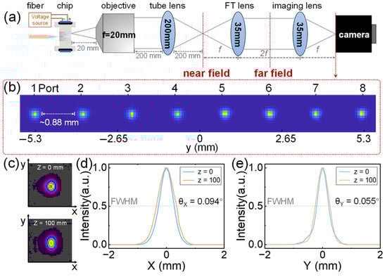
Figure 6.
(a) Measurement setup for far-field. (b) The emission profiles of eight output ports. (c) Far-field emission profiles behind FT lens at a distance of 35 mm (z = 0 mm) and 135 mm (z = 100 mm). The normalized light intensity distributions in the (d) x-direction and (e) y-direction.
Figure 6c shows the patterns behind the FT lens at a distance of 35 mm (z = 0 mm) and 135 mm (z = 100 mm). The beam divergence angles are measured as 0.094° transverse to the waveguide and 0.055° along the waveguide, respectively, as shown in Figure 6d,e.
We then replaced the FT lens with focal lengths of 75 mm and 100 mm to measure the resolution and scanning angles. With these new FT lenses, the resolution and scanning angles were approximately 0.67° and 7.9° for the 75 mm focal length, and 0.5° and 6° for the 100 mm focal length, respectively.
5. Conclusions
In conclusion, we present the first on-chip FPA for optical beam steering operating at the 2 μm wavelength, utilizing cascaded MZI switch array with microheaters on a silicon nitride platform. The device achieves an impressively low excess loss of −1.4 dB. The FPA demonstrates efficient optical beam steering with a FOV of 16.8°and a resolution of 1.43° using an off-chip lens group. The FOV can be effectively enhanced by incorporating additional MZI switch arrays in the system architecture. To achieve an optimal trade-off between FOV expansion and power efficiency, substrate-suspended techniques may be employed [23]. And the background suppression is approximately 17–26 dB. Moreover, by swapping the Fourier transform lens, the system can be adapted to support a wide range of angular steering capabilities. While this work demonstrates 1D beam steering, the architecture can be extended to 2D operation through two potential approaches: (1) integration of an optical Möbius transformation (OMT) module to convert the FPA’s native 1D switching pattern into programmable 2D steering profiles [36], or (2) replacement of edge couplers with wavelength-sensitive grating couplers. In the latter approach, the 1 × 8 MZI switching array would maintain horizontal (X-axis) beam selection while vertical (Y-axis) steering would be achieved through precise wavelength tuning of the laser source [37].
The 2 μm wavelength provides notable advantages, including enhanced sensitivity and reduced scattering for various applications, positioning this work as a significant advancement in Lidar technology within the 2 μm spectral range.
Author Contributions
Methodology, Q.G., J.W. and Y.Z.; Software, D.Y., X.Y. and M.P.; Investigation, Q.G., J.L. and J.W.; Resources, H.X.; Writing—original draft, Q.G.; Writing—review & editing, R.W. and Y.Z.; Visualization, Q.G., J.L. and J.Z.; Supervision, R.W.; Project administration, R.W. and Y.Z.; Funding acquisition, R.W. and Y.Z. All authors have read and agreed to the published version of the manuscript.
Funding
This research was funded by the National Natural Science Foundation of China (NSFC) (62475291, 62335019, 62375293, 62235005) and the Basic and Applied Basic Research Foundation of Guangdong Province (2022A1515012634, 2022B1515130002).
Institutional Review Board Statement
The study did not require ethical approval.
Informed Consent Statement
The study did not involve humans.
Data Availability Statement
Data underlying the results presented in this paper are not publicly available at this time but may be obtained from the authors upon reasonable request.
Acknowledgments
The authors would like to express their sincere gratitude to Siyuan Yu for his invaluable guidance on the research direction and manuscript preparation. We are also deeply grateful to Chunfan Zhu for his excellent assistance in device testing. Special thanks go to Shuqing Lin and Zhaoyang Wu for their expert advice and support in sample processing and device simulation.
Conflicts of Interest
The authors declare no conflicts of interest.
References
- Li, Z.; Heidt, M.A.; Simakov, N.; Jung, Y.; Daniel, O.M.J.; Alam, U.S.; Richardson, J.D. Diode-pumped wideband thulium-doped fiber amplifiers for optical communications in the 1800–2050 nm window. Opt. Express 2011, 21, 26450–26455. [Google Scholar] [CrossRef] [PubMed]
- Lourenço, M.; Gwilliam, R.; Homewood, K. Eye-safe 2 μm luminescence from thulium-doped silicon. Opt. Lett. 2011, 36, 169–171. [Google Scholar] [CrossRef] [PubMed]
- Geng, J.; Wang, Q.; Jiang, S. 2 μm Fiber Laser Sources and Their Applications. In Nanophotonics and Macrophotonics for Space Environments V; SPIE: San Diego, CA, USA, 2011; Volume 8164, pp. 79–88. [Google Scholar]
- Li, K.; Niu, C.; Wu, C.; Yu, Y.; Ma, Y. Development of a 2-μm Solid-State Laser for Lidar in the Past Decade. Sensors 2023, 23, 7024. [Google Scholar] [CrossRef]
- Pal, A.; Sen, R.; Bremer, K.; Yao, S.; Lewis, E.; Sun, T.; Grattan, K.T.V. All-Fiber Tunable Laser in the 2 μm Region Designed for CO2 Detection. Appl. Opt. 2012, 51, 7011–7015. [Google Scholar] [CrossRef] [PubMed]
- Singh, U.N.; Refaat, T.F.; Ismail, S.; Davis, K.J.; Kawa, S.R.; Menzies, R.T.; Petros, M. Feasibility Study of a Space-Based High Pulse Energy 2-μm CO2 IPDA Lidar. Appl. Opt. 2017, 56, 6531–6547. [Google Scholar] [CrossRef]
- Taczak, T.M.; Killinger, D.K. Development of a Tunable, Narrow-Linewidth, CW 2.066-μm Ho:YLF Laser for Remote Sensing of Atmospheric CO2 and H2O. Appl. Opt. 1998, 37, 8460–8476. [Google Scholar] [CrossRef]
- Voisiat, B.; Gaponov, D.; Gečys, P.; Lavoute, L.; Silva, M.; Hideur, A.; Ducros, N.; Račiukaitis, G. Material Processing with Ultra-short Pulse Lasers Working in 2 µm Wavelength Range. In Laser Applications in Microelectronic and Optoelectronic Manufacturing (LAMOM) XX; SPIE: San Diego, CA, USA, 2015; Volume 9350, p. 935014. [Google Scholar]
- Iwai, H.; Aoki, M. Evaluation of a Coherent 2-µm Differential Absorption Lidar for Water Vapor and Radial Wind Velocity Measurements. Opt. Express 2023, 31, 13817–13836. [Google Scholar] [CrossRef]
- Kim, I.; Martins, R.J.; Jang, J.; Badloe, T.; Khadir, S.; Jung, H.-Y.; Kim, H.; Kim, J.; Genevet, P.; Rho, J. Nanophotonics for Light Detection and Ranging Technology. Nat. Nanotechnol. 2021, 16, 508–524. [Google Scholar] [CrossRef]
- Spector, S.J. Review of Lens-Assisted Beam Steering Methods. Opt. Microsyst. 2022, 2, 011003. [Google Scholar] [CrossRef]
- Li, N.; Ho, C.P.; Xue, J.; Lim, L.W.; Chen, G.; Fu, Y.H.; Lee, L.Y.T. A Progress Review on Solid-State LiDAR and Nanophotonics-Based LiDAR Sensors. Laser Photonics Rev. 2022, 16, 2100511. [Google Scholar] [CrossRef]
- Kurosaka, Y.; Iwahashi, S.; Liang, Y.; Sakai, K.; Miyai, E.; Kunishi, W.; Ohnishi, D.; Noda, S. On-Chip Beam-Steering Photonic-Crystal Lasers. Nat. Photonics 2010, 4, 447–450. [Google Scholar] [CrossRef]
- Heck, M.J.R. Highly Integrated Optical Phased Arrays: Photonic Integrated Circuits for Optical Beam Shaping and Beam Steering. Nanophotonics 2017, 6, 93–107. [Google Scholar] [CrossRef]
- Sun, C.; Li, B.; Shi, W.; Lin, J.; Ding, N.; Tsang, H.K.; Zhang, A. Large-Scale and Broadband Silicon Nitride Optical Phased Arrays. IEEE J. Sel. Top. Quantum Electron. 2022, 28, 8200710. [Google Scholar] [CrossRef]
- Sun, C.; Yang, L.; Li, B.; Shi, W.; Wang, H.; Chen, Z.; Nie, X.; Deng, S.; Ding, N.; Zhang, A. Parallel emitted silicon nitride nanophotonic phased arrays for two-dimensional beam steering. Opt. Lett. 2021, 46, 5699–5702. [Google Scholar] [CrossRef] [PubMed]
- Dong, M.; Boyle, J.M.; Palm, K.J.; Zimmermann, M.; Witte, A.; Leenheer, A.J.; Dominguez, D.; Gilbert, G.; Eichenfield, M.; Englund, D. Synchronous Micromechanically Resonant Programmable Photonic Circuits. Nat. Commun. 2023, 14, 7716. [Google Scholar] [CrossRef]
- Inoue, D.; Ichikawa, T.; Kawasaki, A.; Yamashita, T. Demonstration of a New Optical Scanner Using Silicon Photonics Integrated Circuit. Opt. Express 2019, 27, 2499–2508. [Google Scholar] [CrossRef]
- Miller, S.A.; Chang, Y.-C.; Phare, C.T.; Shin, M.C.; Zadka, M.; Roberts, S.P.; Stern, B.; Ji, X.; Mohanty, A.; Gordillo, O.A.J.; et al. Large-Scale Optical Phased Array Using a Low-Power Multi-Pass Silicon Photonic Platform. Optica 2020, 7, 3–6. [Google Scholar] [CrossRef]
- Hutchison, D.N.; Sun, J.; Doylend, J.K.; Kumar, R.; Heck, J.; Kim, W.; Phare, C.T.; Feshali, A.; Rong, H. High-Resolution Aliasing-Free Optical Beam Steering. Optica 2016, 3, 887–890. [Google Scholar] [CrossRef]
- Hsu, C.-P.; Li, B.; Solano-Rivas, B.; Gohil, A.R.; Chan, P.H.; Moore, A.D.; Donzella, V. A Review and Perspective on Optical Phased Array for Automotive LiDAR. IEEE J. Sel. Top. Quantum Electron. 2021, 27, 8300416. [Google Scholar] [CrossRef]
- Li, C.; Cao, X.; Wu, K.; Qiu, G.; Cai, M.; Zhang, G.; Li, X.; Chen, J. Blind Zone-Suppressed Hybrid Beam Steering for Solid-State LiDAR. Photonics Res. 2021, 9, 1871–1880. [Google Scholar] [CrossRef]
- Wu, Z.; Zhang, Y.; Zeng, S.; Lin, S.; Yu, S. Laser Beam Steering of 532 nm Using a Power-Efficient Focal Plane Array. Opt. Lett. 2023, 48, 6400–6403. [Google Scholar] [CrossRef]
- Cui, L.; Wang, P.; Zhao, Q.; Ma, P.; Wang, Z.; Yu, L.; Yang, Y.; Zhang, Y.; Pan, J. Two-Dimensional Scanning of Silicon-Based Focal Plane Array with Field-of-View Splicing Technology. Opt. Express 2023, 31, 1464–1474. [Google Scholar] [CrossRef]
- Mohanty, A.; Li, Q.; Tadayon, M.A.; Roberts, S.P.; Bhatt, G.R.; Shim, E.; Ji, X.; Cardenas, J.; Miller, S.A.; Kepecs, A.; et al. Reconfigurable Nanophotonic Silicon Probes for Sub-Millisecond Deep-Brain Optical Stimulation. Nat. Biomed. Eng. 2020, 4, 223–231. [Google Scholar] [CrossRef]
- Shim, E.; Chen, Y.; Masmanidis, S.; Li, M. Multisite silicon neural probes with integrated silicon nitride waveguides and gratings for optogenetic applications. Sci. Rep. 2016, 6, 22693. [Google Scholar] [CrossRef] [PubMed]
- Rahim, A.; Ryckeboer, E.; Subramanian, A.Z.; Clemmen, S.; Kuyken, B.; Dhakal, A.; Raza, A.; Hermans, A.; Muneeb, M.; Dhoore, S.; et al. Expanding the Silicon Photonics Portfolio with Silicon Nitride Photonic Integrated Circuits. J. Light. Technol. 2017, 35, 639–649. [Google Scholar] [CrossRef]
- Buzaverov, K.A.; Baburin, A.S.; Sergeev, E.V.; Avdeev, S.S.; Lotkov, E.S.; Bukatin, S.V.; Stepanov, I.A.; Kramarenko, A.B.; Amiraslanov, A.S.; Kushnev, D.V.; et al. Silicon Nitride Integrated Photonics from Visible to Mid-Infrared Spectra. Laser Photonics Rev. 2024, 18, 2400508. [Google Scholar] [CrossRef]
- Wang, H.; Chen, Z.; Sun, C.; Deng, S.; Tang, X.; Zhang, L.; Jiang, R.; Shi, W.; Chen, Z.; Li, Z.; et al. Broadband silicon nitride nanophotonic phased arrays for wide-angle beam steering. Opt. Lett. 2021, 46, 286–289. [Google Scholar] [CrossRef]
- Liu, W.; Zhang, K.; Li, B.; Sun, C.; Luo, H.; Shi, W.; Lin, J.; Zhang, A. Blue-Green Wavelength Division Demultiplexing via Polarization-Sensitive Optical Phased Array. J. Light. Technol. 2024, 42, 3807–3813. [Google Scholar] [CrossRef]
- Pisal, A.; Henry, R. Thermo-Optic Switch: Device Structure and Design. In Proceedings of the 2016 2nd International Conference on Advances in Electrical, Electronics, Information, Communication and Bio-Informatics (AEEICB), Chennai, India, 27–28 February 2016; pp. 292–295. [Google Scholar]
- Stegmaier, M.; Ríos, C.; Bhaskaran, H.; Pernice, W.H.P. Thermo-Optical Effect in Phase-Change Nanophotonics. ACS Photonics 2016, 3, 828–835. [Google Scholar] [CrossRef]
- Li, T.; Zhang, H.; Zhou, P.; Lin, Y.; Sun, Y.; Liu, Y.; Xu, X.; Zou, Y. Morphology Engineering Enabled Mid-Infrared Ultra-Dense Waveguide Array with Low Crosstalk. Laser Photonics Rev. 2024, 18, 2400297. [Google Scholar] [CrossRef]
- Gu, T.; Hu, J. Reconfigurable Mid-Infrared Photonics. In Proceedings of the 2021 IEEE Photonics Society Summer Topicals Meeting Series (SUM), Online, 19–21 July 2021; IEEE: Piscataway, NJ, USA, 2021; pp. 1–2. [Google Scholar]
- Lin, H.; Luo, Z.; Gu, T.; Kimerling, L.C.; Wada, K.; Agarwal, A.; Hu, J. Mid-Infrared Integrated Photonics on Silicon: A Perspective. Nanophotonics 2017, 7, 393. [Google Scholar] [CrossRef]
- Yang, D.; He, Q.; Wu, Z.; Wu, L.; Yu, S.; Zhang, Y. Optical Möbius transformation module for expanding beam-steering dimensions. Opt. Laser Technol. 2025, 187, 112784. [Google Scholar] [CrossRef]
- López, J.; Skirlo, S.; Kharas, D.; Sloan, J.; Herd, J.; Juodawlkis, P.; Soljacic, M.; Sorace-Agaskar, C. Planar-lens Enabled Beam Steering for Chip-scale LIDAR. In Proceedings of the 2018 Conference on Lasers and Electro-Optics (CLEO), San Jose, CA, USA, 13–18 May 2018; IEEE: Piscataway, NJ, USA, 2018; pp. 1–2. [Google Scholar]
Disclaimer/Publisher’s Note: The statements, opinions and data contained in all publications are solely those of the individual author(s) and contributor(s) and not of MDPI and/or the editor(s). MDPI and/or the editor(s) disclaim responsibility for any injury to people or property resulting from any ideas, methods, instructions or products referred to in the content. |
© 2025 by the authors. Licensee MDPI, Basel, Switzerland. This article is an open access article distributed under the terms and conditions of the Creative Commons Attribution (CC BY) license (https://creativecommons.org/licenses/by/4.0/).