Article

Polarization-Insensitive Silicon Grating Couplers via Subwavelength Metamaterials and Metaheuristic Optimization

Nanophotonics Technology Center, Universitat Politècnica de València, Camino de Vera s/n, 46022 Valencia, Spain
Photonics 2025, 12(5), 428; https://doi.org/10.3390/photonics12050428
Submission received: 14 April 2025 / Revised: 26 April 2025 / Accepted: 28 April 2025 / Published: 29 April 2025
(This article belongs to the Special Issue Photonics Metamaterials: Processing and Applications)

Abstract

:
Silicon photonics is the leading platform in photonic integrated circuits (PICs), enabling dense integration and low-cost manufacturing for applications such as data communications, artificial intelligence, and quantum processing, to name a few. However, efficient and polarization-insensitive fiber-to-PIC coupling for multipoint wafer characterization remains a challenge due to the birefringence of silicon waveguides. Here, we address this issue by proposing polarization-insensitive grating couplers based on subwavelength dielectric metamaterials and metaheuristic optimization. Subwavelength periodic structures were engineered to act as uniaxial homogeneous linear (UHL) materials, enabling tailored anisotropy. On the other hand, particle swarm optimization (PSO) was employed to optimize the coupling efficiency, bandwidth, and polarization-dependent loss (PDL). Numerical simulations demonstrated that a pitch of 100 nm ensures UHL behavior while minimizing leaky waves. Optimized grating couplers achieved coupling efficiencies higher than −3 dB and a PDL of below 1 dB across the telecom C-band (1530–1565 nm). Three optimization strategies were explored, balancing efficiency, the bandwidth, and the PDL while considering the Pareto front. This work establishes a robust framework combining metamaterial engineering with computational optimization, paving the way for high-performance polarization-insensitive grating couplers with potential uses in advanced photonic applications.

1. Introduction

Along with electronics, which revolutionized the last century, photonics is becoming one of the technological pillars that will face current and forthcoming challenges for humanity. Among these challenges is the exponential growth of data every year, accelerated in recent years by the explosion of artificial intelligence [1,2,3], which in turn significantly increases energy consumption and raises concerns about the environmental sustainability of current infrastructures [4,5]. In this regard, light can address this challenge by encoding information in its “unlimited” bandwidth, thereby providing much more efficient energy consumption per bit [6,7,8,9]. Hence, to leverage light’s benefits, photonic integrated circuits (PICs) pose a suitable technology to reduce costs, allow for dense integration, and implement different functionalities in the same system [10,11,12,13,14,15]. Among the different PIC platforms, silicon photonics is currently the most versatile due to its excellent electronic/optical integration and scalability, achieved by taking advantage of the complementary metal–oxide–semiconductor (CMOS) fabrication processes of the micro- and nano-electronic industry [16,17,18]. Moreover, the high refractive index contrast ( Δ n 2 ) between silicon (Si) and silicon dioxide (SiO2) allows us to confine light in silicon wires with submicron cross-sections. Hence, a large number of emerging and disruptive applications have been demonstrated using silicon photonics, such as quantum processing [19,20,21], neuromorphic computing [22,23,24,25], LiDAR [26,27], and data communications [28], to name a few.
However, silicon photonics still faces some challenges that need to be addressed. The feasibility of efficient, versatile, and polarization-insensitive fiber-to-PIC coupling remains an open question due to the strong birefringence exhibited by silicon waveguides. Several coupling strategies have been proposed based either on edge or vertical coupling [29]. In the first case, the light is coupled by aligning the fiber and the waveguide on the lateral sides of the PIC using spot size converters [30,31,32,33]. In the latter, the fiber is positioned vertically to the top surface of the PIC, and the light beam is coupled to the silicon waveguide by varying the refractive index on the PIC surface using a device coined as a grating coupler [34,35,36,37,38,39,40,41]. Although edge coupling approaches provide low optical losses and negligible wavelength and polarization losses, alignment is critical. They are not as versatile as grating couplers. Therefore, grating couplers are the most popular solution since the structure integrates seamlessly into the PIC and can be placed at any chip position, facilitating multipoint wafer testing. However, the simplest forms suffer from polarization dependence loss (PDL) caused by their phase-matching operation, thereby limiting the system performance and stability against polarization fluctuations.
Therefore, efficient polarization-insensitive grating couplers for a silicon photonics platform are highly appealing [42]. Some approaches based on polarization diversity have been proposed in which a 2D grating coupler can be seen as a superposition of two orthogonally oriented 1D gratings [43,44,45,46]. However, on-chip light is polarized only along a particular axis. Usually, this approach increases the footprint of the PIC. More recent work has harnessed subwavelength dielectric structures [47,48,49]. A wide variety of subwavelength structures have been harnessed for free-space optics, such as metasurfaces [50,51,52]. In this case, such periodic structures behave as lossless metamaterials exhibiting a controlled and tailorable degree of anisotropy [53,54,55]. However, higher design flexibility comes at the cost of a larger design space, making finding the optimal geometrical parameters challenging. In this context, many optimization methods have been employed in nanophotonic devices, offering routes to leverage their full design potential [56].
In this work, we show through numerical simulation the potential of combining such dielectric metamaterials with a metaheuristic optimization method such as particle swarm optimization (PSO) [57] to achieve efficient coupling and polarization-insensitive grating couplers on the silicon-on-insulator (SOI) platform. We provide a comprehensive analysis to determine under what conditions Si/SiO2 subwavelength periodic structures can be approximated to uniaxial homogeneous linear (UHL) materials. Moreover, considering the Pareto front, different configurations and strategies using the PSO algorithm are reported to benefit either the PDL or the coupling efficiency.

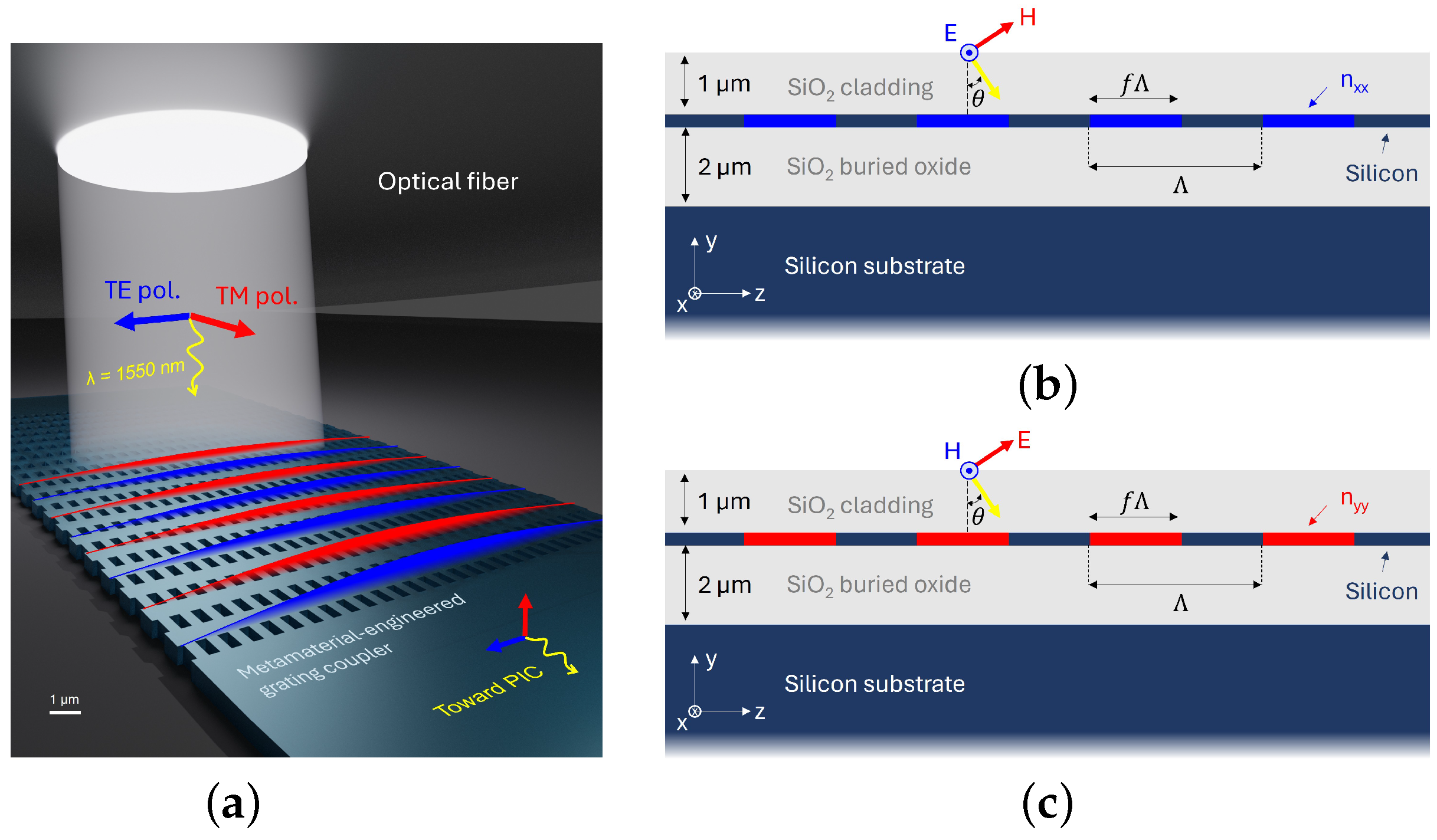
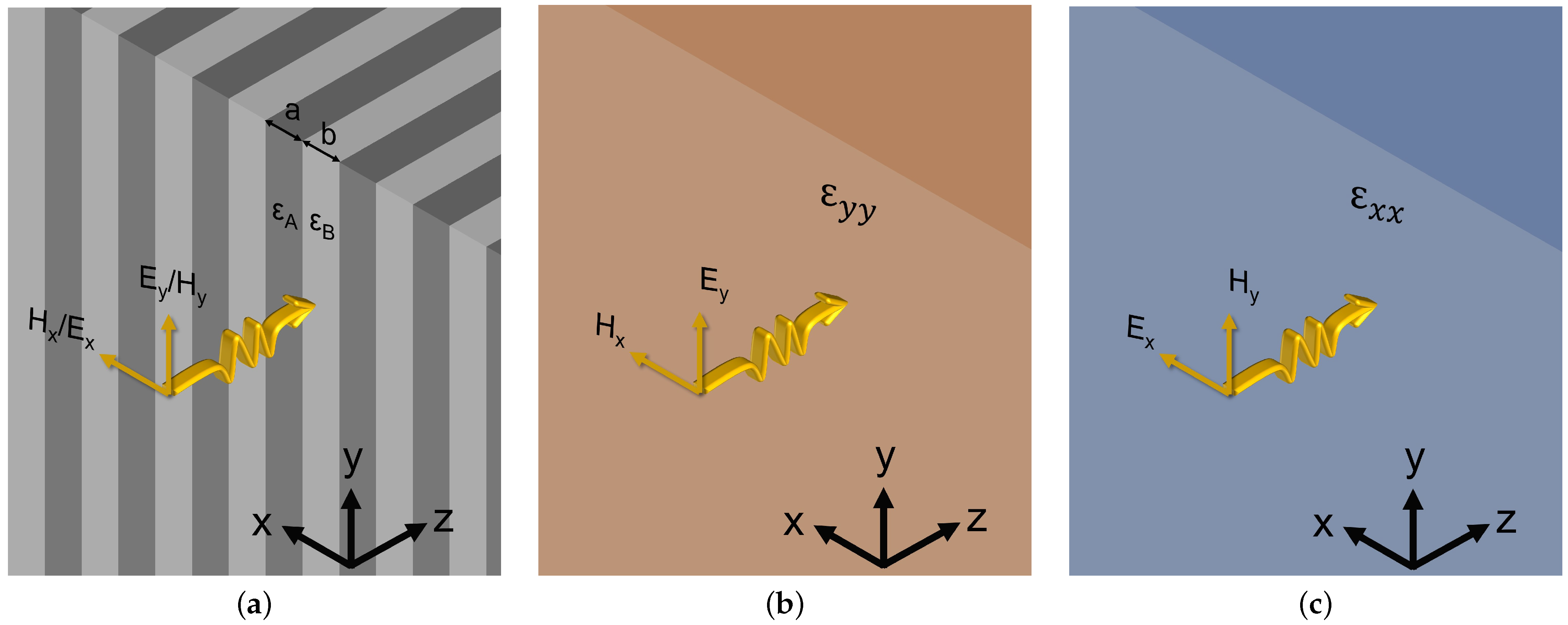
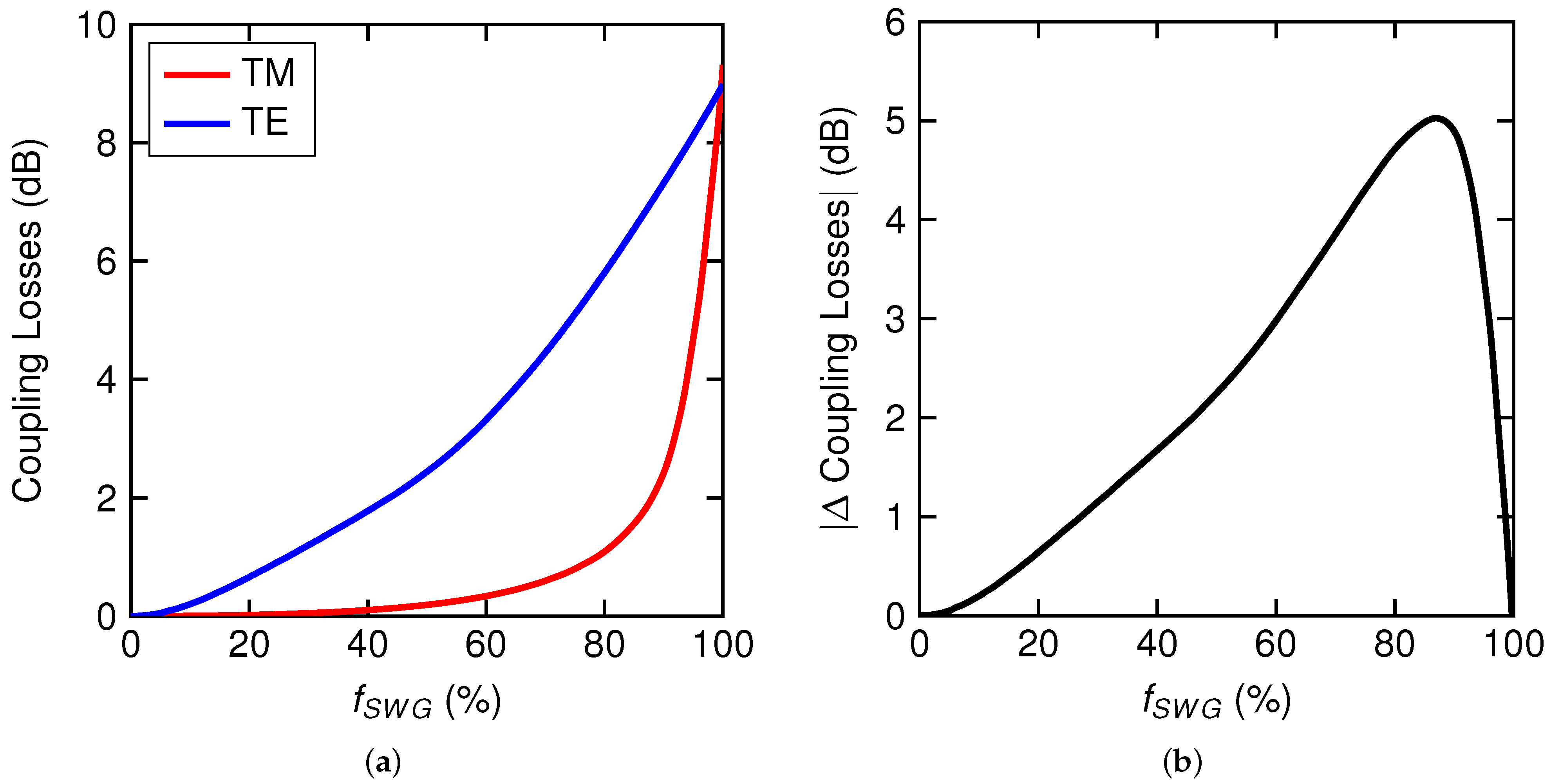
2. Principle of Polarization-Insensitive Grating Couplers Based on Subwavelength Si/SiO2 Metamaterials

In standard silicon grating couplers, the relation between the grating’s pitch and the working wavelength is given by the phase-matching condition [29]:
Λ = λ n g n c sin θ
where  Λ  is the pitch of the grating,  λ  the working wavelength,  n g  the effective refractive index of the light in the grating,  n c  the refractive index of the cladding material, and  θ  the angle of incidence of the light. The value of  n g  can be expressed as
n g = ( 1 f ) n w g + f n e t c h
where f is the fill factor of the etched region with respect to  Λ n w g  is the effective refractive index of the light in the unetched region of the slab waveguide, and  n e t c h  is the effective refractive index of the light in the etched part of the slab waveguide. The value of  n e t c h  will be higher for the fundamental mode of the transverse electric (TE) polarization than the fundamental mode of the transverse magnetic (TM) polarization in silicon slabs. Hence, PDL arises because the grating’s phase-matching condition (Equation (1)) cannot be fulfilled for both polarizations and the same grating’s geometry.
To enable the fulfillment of the polarization independence condition in the grating phase-matching equation [Equation (1)], the value of  n g  must be the same for both polarizations. Thus, the fill factor must fulfill the following conditions:
1 f = 1 + n e t c h T M n e t c h T E n w g T E n w g T M = 1 + Δ n e t c h Δ n w g ,
restricted by  0 < f < 1  and  Δ n w g > 0 . As is shown later, in metamaterial-engineered grating couplers, it is possible to achieve  ( n e t c h T M n e t c h T E ) > 0  and thus a value for f between 0 and 1.
The proposed polarization-insensitive grating coupler is illustrated in Figure 1a. It consists of a one-dimensional grating along the light’s propagation direction (z-axis) made up of unetched and etched silicon regions. The etched regions comprise a periodic stack with a Si/SiO2 subwavelength structure (x-axis) that behaves as a dielectric metamaterial with UHL properties at a 1550 nm wavelength. Due to the UHL behavior of the periodic structure, the equivalent refractive index for the TE,  n x x , and TM,  n y y , polarizations will be different, as shown in Figure 1b and Figure 1c, respectively. Moreover, the equivalent refractive index can be tailored to specific values by playing with the pitch,  Λ S W G , and the fraction of SiO2 f S W G , within a period. Additionally, for this work, we considered a silicon-on-insulator (SOI) platform with a 2  μ m thick buried oxide layer (BOX), 1  μ m thick cladding, and a fiber angle of  10 .

3. Applicability of Effective Medium Theory and Optimal Silicon Thickness

To facilitate the design of the grating coupler through numerical simulations, it was helpful to consider the subwavelength structure as a UHL medium. However, the effective medium theory (EMT) employed to carry out this approximation may not capture certain light phenomena, such as the formation of leaky waves at the interface of two media [58]. Therefore, it is convenient to analyze the impact of the subwavelength pitch in such terms. To this end, we hereinafter focus on the isolated subwavelength metamaterial to analyze its effective medium properties.
Let us consider a periodic structure formed by a stack of two materials with permittivities of  ε A  and  ε B , where light impinges perpendicular to the periodicity. Although the structure in the grating coupler has a finite width, an infinite periodic approximation along the x-axis is valid since the width of grating couplers (∼12  μ m) is much larger than the working wavelength ( 1.55 μ m) [29]. The periodic structure is depicted in Figure 2a, where a plane wave impinges perpendicular to a stack of material of thicknesses a and b with permittivities of  ε A  and  ε B , respectively. The stack is periodic along the x-axis with a pitch of  Λ S W G = a + b  and extends infinitely along both the y- and z-axis. If the relation between the pitch and the incident wave’s wavelength is small enough, then the periodic structures act as a UHL material with the following permittivity tensor:
ε S W G = ε x x 0 0 0 ε y y 0 0 0 ε y y .
Thus, the equivalent metamaterial behaves as a uniaxial crystal with different permittivities depending on whether the light is TM-polarized,  ε y y  (Figure 2b), or TE-polarized,  ε x x  (Figure 2c).
The values of  ε x x  and  ε y y  can be calculated by solving the dispersion relation equation of an infinite two-layer periodic structure [59,60,61]:
cos ( k x Λ S W G ) = cos ( k z , a a ) cos ( k z , b b ) Δ sin ( k z , a a ) sin ( k z , b b )
where
k z , a / b = 2 π λ ε a / b ε S W G
and  Δ  depends on the polarization as
Δ T E = 1 2 ε b k z , a ε a k z , b + ε a k z , b ε b k z , a
and
Δ T M = 1 2 k z , a k z , b + k z , b k z , a .
Since the light propagates only along the z-axis, the term  k x  equals zero.
Equation (5) has no analytical solution, and numeric root-finding methods are necessary. However, suppose the pitch–wavelength relation is small enough. In that case, it can be accurately approximated to the zero order of a Taylor expansion by using an EMT model such as the Maxwell Garnett model [62]. For this kind of structure, the approximations for both polarizations are the well-known Rytov’s formulas [63], given by Equations (9) and (10) for TM and TE polarization, respectively. A second-order approximation can be utilized if the relation is not small enough. Nevertheless, obtaining the exact solution by solving Equation (5) is preferred to obtain much higher accuracy.
ε y y = a Λ S W G ε A + b Λ S W G ε B
1 ε x x = a Λ S W G 1 ε A + b Λ S W G 1 ε B
However, it is difficult to rigorously define the term “small enough” and thereby approximate the metamaterial as an equivalent UHL medium. On the other hand, by using Bragg’s condition, it can be proved that if the pitch fulfills
Λ S W G < λ max ( ε A , ε B )
then diffraction is not allowed, and the light travels through the subwavelength structure with a phase given by the dispersion relation expression [Equation (5)]. However, this does not mean the subwavelength structure behaves as a homogeneous material. If  Λ / λ 0  is not accomplished, leaky waves could arise at the interface, which could tunnel through the grating structure if it is not long enough and affect its performance. Hence, the material cannot be treated as homogeneous.
Setting a value of  Λ S W G  for which the subwavelength structure can be treated as a UHL medium is not trivial. Here, we have analyzed the following aspects: (i) the dispersion relation equation, (ii) the field profile inside the periodic structure, and (iii) the transmittance/reflectance values when it is interfaced with a homogeneous material. In the following analysis, we consider a stack comprised of Si ( ε r = 12.08 ) and SiO2 ( ε r = 2.085 ) at  λ = 1550  nm. Moreover, for the ease of calculations, the thickness of both layers is set to  a = b = Λ S W G / 2 .

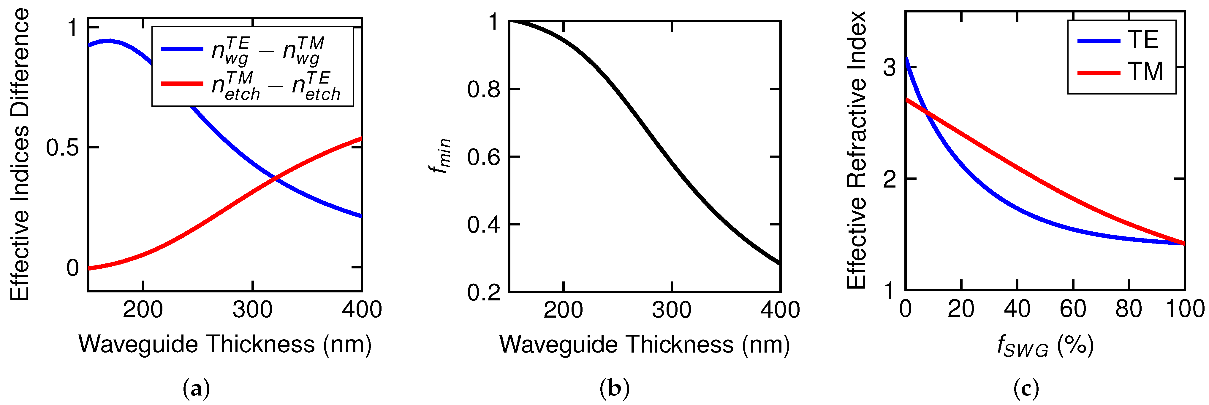
3.1. Equivalent Refractive Index
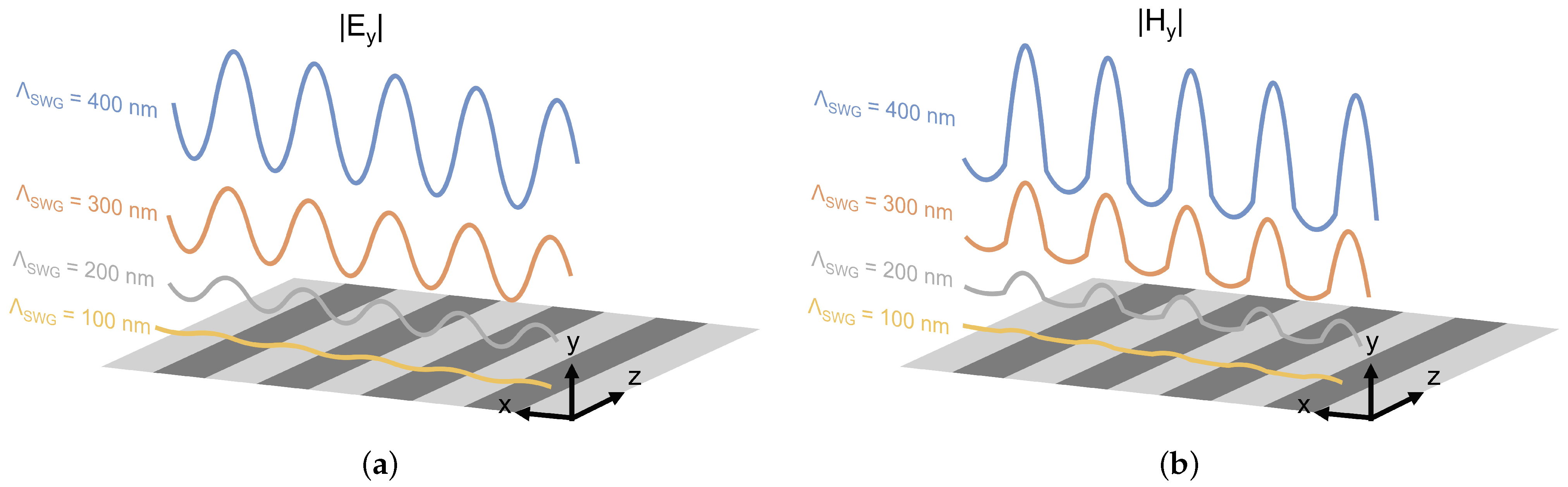
The dispersion relation equation [Equation (5)] was first investigated by obtaining the real solutions for both polarizations as a function of the pitch, thus yielding an equivalent refractive index,  n e q . As shown in Figure 3a, for pitch values lower than  λ / n S i = 445  nm, only the zero order was allowed, in agreement with Equation (11), and the structure is in the subwavelength regime. It has to be noticed that the lower the pitch, the higher the birefringence between the effective refractive index of both polarizations. As discussed later, large birefringence values are beneficial for designing polarization-insensitive grating couplers. When the subwavelength condition is not fulfilled, high-order modes begin to arise. In contrast, when  Λ S W G + , all the solutions converge to plane waves.
A comparison between the rigorous solution given by Equation (5) and Rytov’s approximation [Equations (10) and (9)] is shown in Figure 3b. As can be noticed, the approximation was only accurate for pitch values lower than ∼100 nm. For higher values, it could only be used to estimate the values of the equivalent refractive index.
Regarding the imaginary solutions corresponding to leaky waves, we observed differences between those obtained from approximating the periodic stack as an equivalent homogeneous material and solving Equation (5). In a homogeneous medium, the imaginary solutions of  n e q  are antisymmetric, i.e.,  n e q , m = n e q , m , where m is the mth imaginary solution. However, in a periodic subwavelength medium, the solutions given by Equation (5) are not antisymmetric and are only approximate when  Λ S W G 100  nm.

3.2. Field Profile

Recalling Maxwell’s equations, a plane wave traveling through a homogeneous medium has only one component in both the E- and H-fields, with a constant value in the axis transverse (x-axis) to the propagation direction (z-axis). However, in a crosswise subwavelength periodic medium, two components (transverse and longitudinal) exist in the E- or H-field (depending on the polarization). The different profiles of the field components were obtained by implementing the transfer matrix method (TMM) in MATLAB 2020a [61].
The transverse components for TE and TM polarizations are depicted in Figure 4a and Figure 4b, respectively, for different pitch values. The amplitude diminishes as the pitch is reduced, making it negligible for pitch values lower than 100 nm, thereby approximating a plane wave in a homogeneous medium.
On the other hand, the impact of the longitudinal component can be visualized by representing the ellipse of polarization. These ellipses are plotted for different pitch values in Figure 5a and Figure 5b for TE ( E x  and  E z ) and TM ( H x  and  H z ) polarization, respectively. The ellipse was calculated at the interface of the Si/SiO2 stack. The interface point was chosen since the longitudinal component attained its maximum value. As noted, for both polarizations, the polarization ellipse tended to shrink as the pitch was reduced, i.e., only the transverse component, as in a homogeneous medium, existed. Moreover, for TE polarization, this was more pronounced than for TM polarization because in the latter,  E z ε ( x ) . On the other hand, the axial ratio was obtained as  | ϕ x / ϕ z |  and is depicted in Figure 5c. For a plane wave, the axial ratio is infinity; however, in a subwavelength medium, this is not accomplished, as noted.

3.3. Interface with Homogeneous Material

A non-constant field along the x-axis must be considered when the subwavelength structure is interfaced with a homogeneous material. To fulfill boundary conditions, significant leaky waves may arise at the interface, thus making it inaccurate to treat the periodic stack as a homogeneous material.
To analyze this behavior, we considered the previous SiO2/Si stack (medium II) interfaced with silicon (medium I). A plane wave traveled along the z-axis from medium I and impinged to medium II. The field profile at the interface of Si and the Si/SiO2 stack and each medium was obtained using the eigenmode expansion method [64]. In contrast with other simulation methods such as the finite-difference time domain (FDTD), the utilization of eigenmode expansion allowed for discrimination between the propagating modes ( m = 0 ) and the leaky modes ( m 0 ) and thus for gaining insight into the phenomena that occurred within the structure. Calculations were carried out for both polarizations and pitch values of 400 and 100 nm.
In Figure 6, the field distribution (x,z) is depicted for  Λ S W G = 400  nm of the  | E y |  (Figure 6a) and  | H y |  (Figure 6b) components for the TM- and TE-polarized waves, respectively. As can be noticed, leaky modes at the interface perturb the adjoint wave between the two media for both polarizations. However, for TE polarization, they extend further along the z-axis. Such leaky modes arise to satisfy the continuous condition of the tangential electric field at the interface between the two media. Therefore, if several homogeneous/subwavelength media are stacked along the z-axis, as in grating couplers, leaky waves may interact with the propagated wave, giving rise to optical perturbations. Consequently, the subwavelength medium cannot be approximated as being homogeneous. In contrast, if the value of  Λ S W G  is reduced to 100 nm, leaky waves are negligible, as shown in Figure 7, and thus, a homogeneous approximation can be accurate.
Therefore, based on these results, we chose  Λ S W G = 100  nm for the design of our polarization-insensitive grating coupler. Figure 8a shows the equivalent refractive index as a function of the filling factor using the zero-order approximation given by Rytov. As can be noticed, TM polarization exhibits a larger refractive index than TE polarization, which could enable the fulfillment of the polarization independence condition of the grating coupler. Moreover, the birefringence,  Δ n , can be as large as 0.8 for filling factors of around 40% and greater than 0.2 for almost the whole range (see Figure 8b).

3.4. Optimal Thickness of Silicon

The thickness of the silicon layer plays a vital role in a grating coupler’s performance. A thick silicon layer provides a broader range of tunability in the equivalent refractive index of the metamaterial. The best case or lower limit of the fill factor is given when  Δ n e t c h  attains its maximum value, i.e., when the subwavelength structure achieves the maximum birefringence ( f S W G = 0.4 ). For the latter, the values of  Δ n w g  and  Δ n e t c h  are depicted as a function of the waveguide thickness in Figure 9a. As the thickness increases from the standard 220 nm, the difference between both increments decreases until it reaches around 320 nm. The associated minimum value of f is shown in Figure 9b. Thick waveguide thicknesses may not be appropriate as they are highly multimodal and more sensitive to environmental variations such as the temperature. Thus, considering this trade-off, we chose 320 nm as the thickness for the silicon layer of the gratings. On the other hand, regarding the upper limit of the fill factor, this is achieved when  n e t c h T M n e t c h T E = 0 . For a 320 nm thick waveguide, this yields a  f S W G  value of between 7% and 99.6% (see Figure 8). Finally, minimum feature sizes below 10 nm can be obtained by electron beam lithography (EBL) [65,66] and are expected to be improved using photolithography in silicon photonic foundries. Hence, the upper and lower bounds of  f S W G  were set to 0.1 and 0.9, respectively.

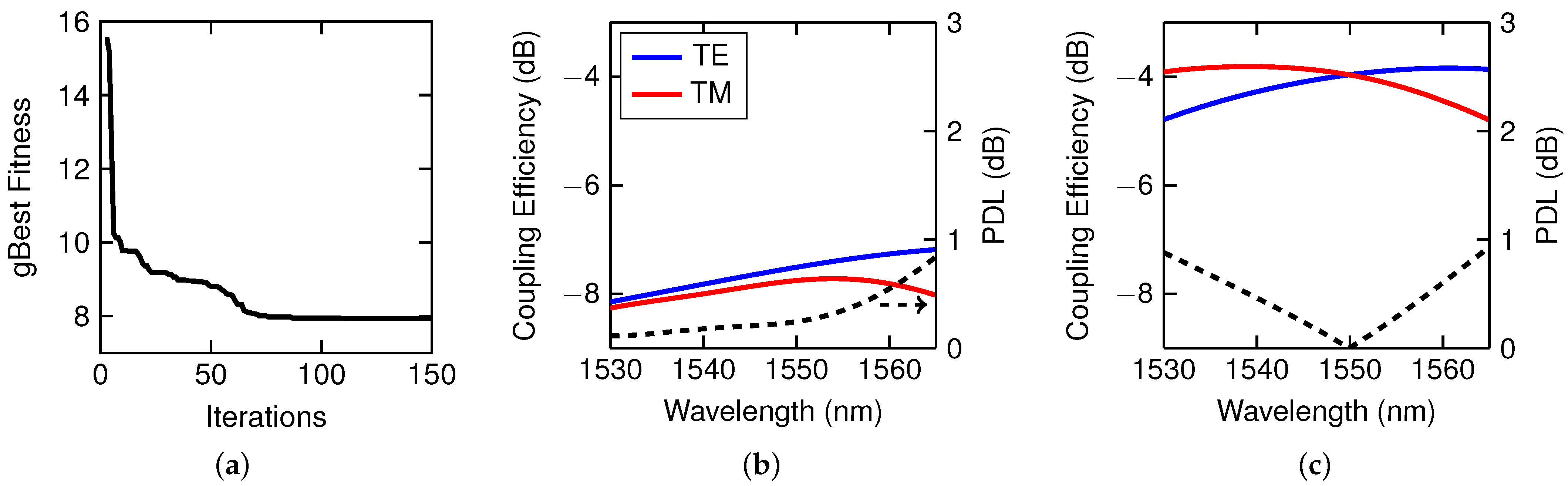
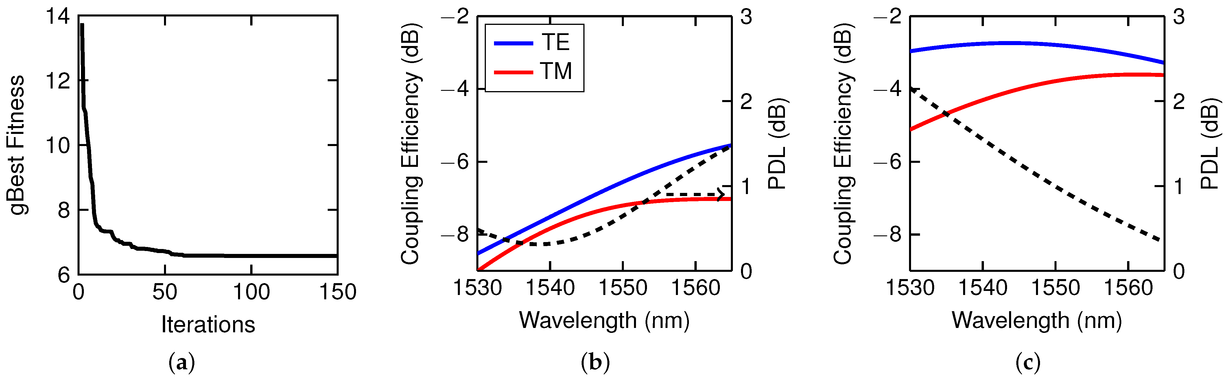
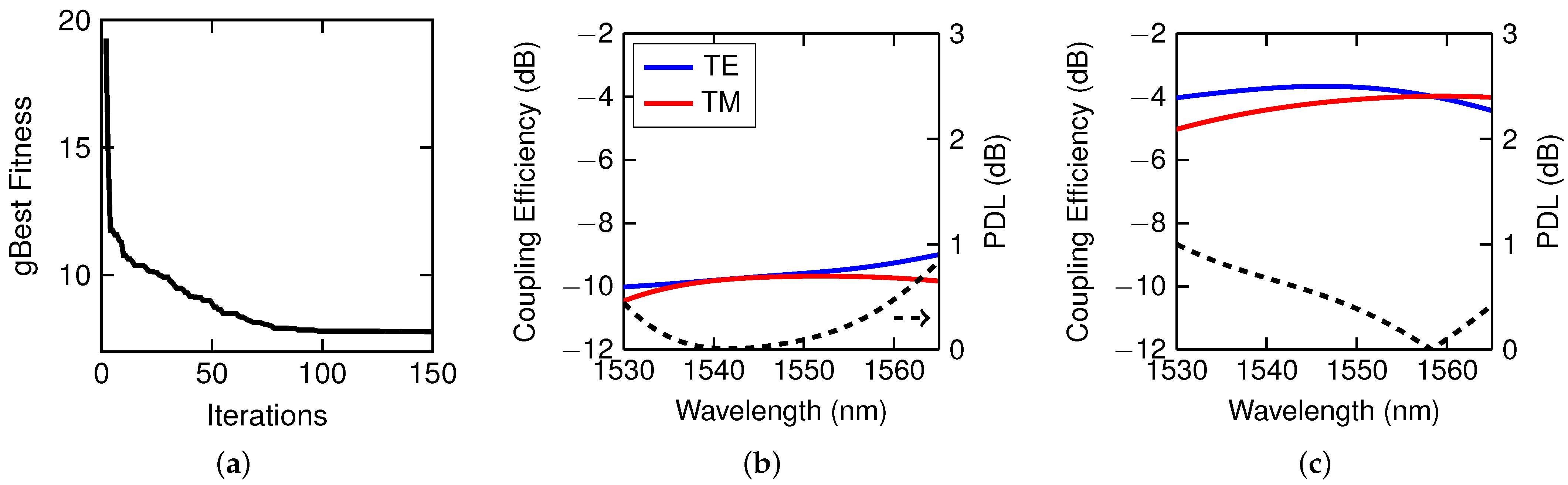
4. Achieving High Optical Performance via Particle Swarm Optimization

The phase-matching condition can be fulfilled for both polarizations using a large set of  f S W G  values. However, each solution yields a different grating coupler performance. Indeed, the diffraction strength, i.e., the amount of power that is diffracted due to the impedance mismatch of different waveguides, is different for both polarizations. Figure 10a shows the coupling losses between a 320 nm thick Si slab waveguide and a metamaterial slab waveguide comprising the subwavelength structure as a function of the  f S W G  value. The coupling losses are higher for TE polarization because it presents a more significant impedance mismatch than TM polarization. The difference in the diffraction strength is increased with the fill factor achieving its maximum at  f S W G 85 % , as shown in Figure 10b. Hence, the optimization of each grating period should be carried out to ensure the maximum performance.
As mentioned in the Introduction, in this work, optimization is based on the metaheuristic method of PSO. The flow chart of the implemented PSO algorithm is depicted in Figure 11. This begins with the initialization of the particles that comprise the swarm. The swarm consists of N particles, with each particle being M-dimensional. In our case, a particle represents a grating coupler, for which the variables are  f S W G λ T E , and  λ T M . The wavelength values are set as variables for greater freedom during optimization. Then, the following steps are repeated  I m a x  times. First, the performance of the particles is evaluated using the fitness, which assigns a cost to each particle. If each particle’s cost is better (lower) than in the previous iteration, then the pBest (particle’s best) is updated. Moreover, among the particles, their positions are compared to the gBest (global best), saving the best particle from all iterations. When the pBests and gBest are updated, if required, the velocity of each particle is updated to obtain their new position.
The velocity of the particles is calculated by using the following expression:
v i + 1 ( n , m ) = w i v i ( n , m ) + c 1 r 1 g i ( m ) x i ( n , m ) + c 2 r 2 p i ( n , m ) x i ( n , m )
where w is the inertia weight that prevents the particle from drastically changing its direction,  c 1  is the cognitive coefficient that is related to the memory of the previous best position,  c 2  is the social coefficient and relates to the neighbors, r is a random number between 0 and 1 following a uniform distribution,  x i ( n , m )  stands for the current position, and  p i ( n , m )  and  g i ( m )  are the particle’s best position and the global best position, respectively. The coefficients  c 1  and  c 2  impose a trade-off between exploration and exploitation, i.e., the ability to explore various regions of the search space or to concentrate the search around a promising area, respectively. For instance, if  c 1 = c 2 > 0 , particles are attracted toward the average of the personal best position and the global best position. On the other hand,  c 2 > c 1  is more beneficial for unimodal problems, whereas  c 2 < c 1  is better for multimodal problems. Then, the position is updated as
x i + 1 ( n , m ) = x i ( n , m ) + v i + 1 ( n , m )
Every nature-inspired algorithm is not exempt from potential issues. The most common are related to convergence. For instance, the optimal solution can stick to a local minimum, or the particle position goes out of the boundaries. Several solutions have been proposed to tackle these problems [67]. Among them, in this work, we used the following strategies:
  • Usually, the positions of particles are initialized to cover the search space uniformly. An efficient initialization method for the particle position is
    x 0 ( n , m ) = x min + r ( x max x min )
  • To control the global exploration of particles, velocities are clamped to stay within the boundary constraints. The velocity clamping is defined as
    v i + 1 ( n , m ) = v i + 1 ( n , m ) if v i + 1 ( n , m ) < v max v max if v i + 1 ( n , m ) v max
    where  v max = k ( v u b v l b ) , with k being a constant between 0 and 1 and  v u p  and  v l b  the upper and lower boundaries of the velocity, respectively. On the other hand, if the particle is about to go beyond the boundary limits, the velocity is set randomly to set the next position of the particle within the boundaries.
  • The inertia weight value is problem-dependent. A common strategy is to start with a large value to facilitate exploration and linearly decrease its value to promote exploitation. Thus,
    w i = w 0 w I m a x I m a x i I m a x + w I m a x
    where  w 0 = 0.9  and  w I m a x = 0.4 .
  • PSO can find optimal solutions with a small population of between 10 and 30. In this work, we employed 25 particles.
  • Particles draw their strength from their cooperative nature and are more effective when nostalgia ( c 1 ) and envy ( c 2 ) coexist in a good balance ( c 1 c 2 ).
Table 1 shows the parameters utilized for all optimization cases.
The fitness of the solutions is assessed by defining a figure of merit (FOM) that includes the following metrics: the coupling efficiency (CE), bandwidth (BW), PDL, and PDL BW. The FOM gives a value that should be minimized in this case. Defining the right FOM is crucial to obtaining the best solution, and its definition depends on the required specifications. However, one must keep in mind that trade-offs exist among these metrics, and not all can be improved at the same time, known as the Pareto front, in which one parameter or some parameters will not be improved without diminishing others [68].
High coupling, efficiency, and a large bandwidth are desired in a grating coupler. However, there is a trade-off between them (2D Pareto front). Moreover, in a polarization-insensitive grating coupler, the PDL and its bandwidth are included as extra parameters, which extends the Pareto front to four dimensions. The dependence among the four parameters is reflected in Figure 12.
This work considered using grating couplers to cover the telecom C-band (1530–1565 nm) while maximizing the coupling efficiency at 1550 nm. The number of grating periods was fixed at 20. On the other hand, since the perfect coupler does not exist according to Figure 12, three different FOMs were proposed depending on the critical parameter to improve, while the others could be relaxed. The first FOM included all four parameters [Equation (17)] and tried to balance them. The second one was focused on the coupling efficiency, and the PDL and bandwidth constraints were relaxed [Equation (18)]. Finally, the last FOM relaxed the performance at 1550 nm and aimed to cover the entire C-band with PDLs of lower than 1 dB [Equation (19)]. The values of the PDL and CE were calculated in dB and were obtained at 1550 nm, while the bandwidth had nanometer units and was clipped to within the C-band wavelength range (35 nm).
F O M = 35 B W P D L P D L 35 B W T E C E T E 35 B W T M C E T M
F O M = C E T E + C E T M max 1 , P D L
F O M = C E T E + C E T M 35 B W P D L 8
The PSO algorithm was implemented using an in-house script adapted to the RSoft commercial simulation tool [69], which was employed to calculate the optical metrics of the grating couplers using the 2D-FDTD method. Other numerical simulation tools combining the FDTD method with a built-in PSO optimizer could be employed with the proposed PSO settings and workflow.
For the first case, the evolution of the gBest fitness as a function of the iterations is shown in Figure 13a. The cost of the gBest rapidly decreased in the first few iterations. This behavior was attributed to the size of the swarm and the promotion of exploration. Afterward, the cost decreased at a slow pace and converged from the 100th iteration. The spectra for the gBest particle at the beginning and at the end of the optimization are depicted in Figure 13b and Figure 13c, respectively. At the beginning, the PDLs were very low because of the low coupling efficiency for both polarizations (see Figure 12). For the final spectra, the coupling efficiencies were increased from  7.5  dB to  4  dB while keeping the PDL lower than 1 dB across the entire C-band.
The optimized grating’s physical parameters can be found in the Supplementary Materials. Most of the  f S W G  values were between 35% (35 nm) and 75% (75 nm). Thus, the footprint of the structures was far from the e-beam lithography minimum feature size.
The algorithm converged in the first iterations for the second FOM, as seen in Figure 14a. The initial spectra did not meet the requirement of having less than 1 dB for the PDL at 1550 nm. Moreover, the coupling efficiencies were quite low (see Figure 14b). These values were improved by the end of the optimization, as shown in Figure 14c. The PDL was lower than 1 dB. However, the PDL bandwidth was narrower than in the first case since this metric was not included in the FOM. Regarding the coupling efficiencies, these suffered an increase of up to 5 dB, and values of as high as  2.5  dB were achieved for TE polarization. The geometrical values of the optimized structures can be found in the Supplementary Materials. In this regard, it would be feasible to fabricate these by e-beam lithography.
Finally, for the third analyzed case, the PSO converged similarly to in FOM #1, as seen in Figure 15a. Although the initial spectra met the requirement of having a PDL bandwidth in the C-band with PDLs lower than 1 dB, the coupling efficiencies were relatively low (see Figure 15b). After the optimization, the PDL requirements were still met, but the coupling efficiencies improved by more than 5 dB, as shown in Figure 14c. The physical values corresponding to the last FOM are summarized in the Supplementary Materials. As in the previous designs, the values were within the boundaries, and the physical parameters would be feasible to fabricate.
The final metrics of the optimized gratings for the different FOMs are summarized in Table 2. The final geometries of the optimized grating couplers are listed in the Supplementary Materials. The overall best grating performance was achieved with the grating corresponding to FOM #1. The grating of FOM #2 presented a better CE for TE polarization but at the cost of a lower bandwidth and an increase in the PDL. Finally, the grating of FOM #3 covered the entire C-band with a PDL lower than 1 dB but with slightly worse CE values than FOM #1 since this parameter was not evaluated in this FOM.

5. Conclusions

In this work, we have demonstrated the potential of polarization-insensitive silicon grating couplers designed using subwavelength metamaterials and the PSO method. The proposed approach achieved efficient coupling with a minimal PDL by leveraging the anisotropic properties of Si/SiO2 subwavelength structures. Our numerical simulations confirmed that a 100 nm subwavelength pitch ensures UHL behavior in such subwavelength structures by negating the influence of leaky waves. On the other hand, a silicon thickness of 320 nm delivered a broad tunable range for the metamaterial’s fill factor. The optimized grating couplers achieved coupling efficiencies exceeding  3  dB and a PDL below 1 dB across the telecom C-band (1530–1565 nm). Three optimization strategies were explored, revealing trade-offs between the coupling efficiency, bandwidth, and PDL through Pareto front analysis. Moreover, our designs are compatible with standard CMOS fabrication processes employed for silicon-based integrated photonics and coupler devices, such as e-beam lithography and reactive ion etching [29].
Therefore, our work establishes a robust framework combining metamaterial engineering with computational optimization, paving the way for advanced photonic devices. The findings are particularly relevant for photonic applications in telecommunications, quantum technologies, and artificial intelligence, where high performance and polarization insensitivity are vital.

Supplementary Materials

The following supporting information can be downloaded at https://www.mdpi.com/article/10.3390/photonics12050428/s1: Table S1: Geometrical grating coupler parameters obtained for FOM #1; Table S2: Geometrical grating coupler parameters obtained for FOM #2; Table S3: Geometrical grating coupler parameters obtained for FOM #3.

Funding

This research was partly funded by the Universitat Politècnica de València, grants PAID-10-23 and PAID-06-23, and partly by grant PID2022-137787OB-I00, funded by MCIN/AEI/10.13039/501100011033.

Institutional Review Board Statement

Not applicable.

Informed Consent Statement

Not applicable.

Data Availability Statement

The original contributions presented in this study are included in the article/Supplementary Material. Further inquiries can be directed to the corresponding author.

Conflicts of Interest

The authors declare no conflicts of interest.

References

  1. Marx, V. The big challenges of big data. Nature 2013, 498, 255–260. [Google Scholar] [CrossRef] [PubMed]
  2. Lord, A.; Soppera, A.; Jacquet, A. The impact of capacity growth in national telecommunications networks. Philos. Trans. R. Soc. A Math. Phys. Eng. Sci. 2016, 374, 20140431. [Google Scholar] [CrossRef] [PubMed]
  3. Liang, W.; Tadesse, G.A.; Ho, D.; Li, F.; Zaharia, M.; Zhang, C.; Zou, J. Advances, challenges and opportunities in creating data for trustworthy AI. Nat. Mach. Intell. 2022, 4, 669–677. [Google Scholar] [CrossRef]
  4. Wu, C.J.; Raghavendra, R.; Gupta, U.; Acun, B.; Ardalani, N.; Maeng, K.; Chang, G.; Behram, F.A.; Huang, J.; Bai, C.; et al. Sustainable AI: Environmental Implications, Challenges and Opportunities. arXiv 2022, arXiv:2111.00364. [Google Scholar]
  5. Crawford, K. Generative AI’s environmental costs are soaring—And mostly secret. Nature 2024, 626, 693. [Google Scholar] [CrossRef]
  6. Shastri, B.J.; Tait, A.N.; Ferreira De Lima, T.; Pernice, W.H.P.; Bhaskaran, H.; Wright, C.D.; Prucnal, P.R. Photonics for artificial intelligence and neuromorphic computing. Nat. Photonics 2021, 15, 102–114. [Google Scholar] [CrossRef]
  7. Winzer, P.J.; Neilson, D.T. From Scaling Disparities to Integrated Parallelism: A Decathlon for a Decade. J. Light. Technol. 2017, 35, 1099–1115. [Google Scholar] [CrossRef]
  8. Winzer, P.J.; Neilson, D.T.; Chraplyvy, A.R. Fiber-optic transmission and networking: The previous 20 and the next 20 years [Invited]. Opt. Express 2018, 26, 24190. [Google Scholar] [CrossRef]
  9. Bourzac, K. Fixing AI’s energy crisis. Nature, 2024; online ahead of print. [Google Scholar] [CrossRef]
  10. Siew, S.Y.; Li, B.; Gao, F.; Zheng, H.Y.; Zhang, W.; Guo, P.; Xie, S.W.; Song, A.; Dong, B.; Luo, L.W.; et al. Review of Silicon Photonics Technology and Platform Development. J. Light. Technol. 2021, 39, 4374–4389. [Google Scholar] [CrossRef]
  11. Smit, M.; Williams, K.; Van Der Tol, J. Past, present, and future of InP-based photonic integration. APL Photonics 2019, 4, 050901. [Google Scholar] [CrossRef]
  12. Blumenthal, D.J.; Heideman, R.; Geuzebroek, D.; Leinse, A.; Roeloffzen, C. Silicon Nitride in Silicon Photonics. Proc. IEEE 2018, 106, 2209–2231. [Google Scholar] [CrossRef]
  13. Li, N.; Ho, C.P.; Zhu, S.; Fu, Y.H.; Zhu, Y.; Lee, L.Y.T. Aluminium nitride integrated photonics: A review. Nanophotonics 2021, 10, 2347–2387. [Google Scholar] [CrossRef]
  14. Zhu, D.; Shao, L.; Yu, M.; Cheng, R.; Desiatov, B.; Xin, C.J.; Hu, Y.; Holzgrafe, J.; Ghosh, S.; Shams-Ansari, A.; et al. Integrated photonics on thin-film lithium niobate. Adv. Opt. Photonics 2021, 13, 242. [Google Scholar] [CrossRef]
  15. Abel, S.; Eltes, F.; Ortmann, J.E.; Messner, A.; Castera, P.; Wagner, T.; Urbonas, D.; Rosa, A.; Gutierrez, A.M.; Tulli, D.; et al. Large Pockels effect in micro- and nanostructured barium titanate integrated on silicon. Nat. Mater. 2019, 18, 42–47. [Google Scholar] [CrossRef]
  16. Dong, P.; Chen, Y.K.; Duan, G.H.; Neilson, D.T. Silicon photonic devices and integrated circuits. Nanophotonics 2014, 3, 215–228. [Google Scholar] [CrossRef]
  17. Lipson, M. The revolution of silicon photonics. Nat. Mater. 2022, 21, 974–975. [Google Scholar] [CrossRef]
  18. Shekhar, S.; Bogaerts, W.; Chrostowski, L.; Bowers, J.E.; Hochberg, M.; Soref, R.; Shastri, B.J. Roadmapping the next generation of silicon photonics. Nat. Commun. 2024, 15, 751. [Google Scholar] [CrossRef]
  19. Sibson, P.; Kennard, J.E.; Stanisic, S.; Erven, C.; O’Brien, J.L.; Thompson, M.G. Integrated silicon photonics for high-speed quantum key distribution. Optica 2017, 4, 172. [Google Scholar] [CrossRef]
  20. Moody, G.; Sorger, V.J.; Blumenthal, D.J.; Juodawlkis, P.W.; Loh, W.; Sorace-Agaskar, C.; Jones, A.E.; Balram, K.C.; Matthews, J.C.F.; Laing, A.; et al. 2022 Roadmap on integrated quantum photonics. J. Phys. Photonics 2022, 4, 012501. [Google Scholar] [CrossRef]
  21. Harris, N.C.; Bunandar, D.; Pant, M.; Steinbrecher, G.R.; Mower, J.; Prabhu, M.; Baehr-Jones, T.; Hochberg, M.; Englund, D. Large-scale quantum photonic circuits in silicon. Nanophotonics 2016, 5, 456–468. [Google Scholar] [CrossRef]
  22. Xu, B.; Huang, Y.; Fang, Y.; Wang, Z.; Yu, S.; Xu, R. Recent Progress of Neuromorphic Computing Based on Silicon Photonics: Electronic–Photonic Co-Design, Device, and Architecture. Photonics 2022, 9, 698. [Google Scholar] [CrossRef]
  23. Farmakidis, N.; Dong, B.; Bhaskaran, H. Integrated photonic neuromorphic computing: Opportunities and challenges. Nat. Rev. Electr. Eng. 2024, 1, 358–373. [Google Scholar] [CrossRef]
  24. El Srouji, L.; Krishnan, A.; Ravichandran, R.; Lee, Y.; On, M.; Xiao, X.; Ben Yoo, S.J. Photonic and optoelectronic neuromorphic computing. APL Photonics 2022, 7, 051101. [Google Scholar] [CrossRef]
  25. Kutluyarov, R.V.; Zakoyan, A.G.; Voronkov, G.S.; Grakhova, E.P.; Butt, M.A. Neuromorphic Photonics Circuits: Contemporary Review. Nanomaterials 2023, 13, 3139. [Google Scholar] [CrossRef]
  26. Zhang, X.; Kwon, K.; Henriksson, J.; Luo, J.; Wu, M.C. A large-scale microelectromechanical-systems-based silicon photonics LiDAR. Nature 2022, 603, 253–258. [Google Scholar] [CrossRef]
  27. Sun, X.; Zhang, L.; Zhang, Q.; Zhang, W. Si Photonics for Practical LiDAR Solutions. Appl. Sci. 2019, 9, 4225. [Google Scholar] [CrossRef]
  28. Shi, Y.; Zhang, Y.; Wan, Y.; Yu, Y.; Zhang, Y.; Hu, X.; Xiao, X.; Xu, H.; Zhang, L.; Pan, B. Silicon photonics for high-capacity data communications. Photonics Res. 2022, 10, A106. [Google Scholar] [CrossRef]
  29. Marchetti, R.; Lacava, C.; Carroll, L.; Gradkowski, K.; Minzioni, P. Coupling strategies for silicon photonics integrated chips [Invited]. Photonics Res. 2019, 7, 201. [Google Scholar] [CrossRef]
  30. Larrea, R.; Gutierrez, A.M.; Griol, A.; Brimont, A.; Sanchis, P. Fiber-to-Chip Spot-Size Converter for Coupling to Silicon Waveguides in the O-Band. IEEE Photonics Technol. Lett. 2019, 31, 31–34. [Google Scholar] [CrossRef]
  31. Galán, J.V.; Sanchis, P.; Sánchez, G.; Martí, J. Polarization insensitive low-loss coupling technique between SOI waveguides and high mode field diameter single-mode fibers. Opt. Express 2007, 15, 7058. [Google Scholar] [CrossRef] [PubMed]
  32. Fang, Q.; Liow, T.Y.; Song, J.F.; Tan, C.W.; Yu, M.B.; Lo, G.Q.; Kwong, D.L. Suspended optical fiber-to-waveguide mode size converter for Silicon photonics. Opt. Express 2010, 18, 7763. [Google Scholar] [CrossRef]
  33. Almeida, V.R.; Panepucci, R.R.; Lipson, M. Nanotaper for compact mode conversion. Opt. Lett. 2003, 28, 1302. [Google Scholar] [CrossRef]
  34. Taillaert, D.; Laere, F.V.; Ayre, M.; Bogaerts, W.; Thourhout, D.V.; Bienstman, P.; Baets, R. Grating Couplers for Coupling between Optical Fibers and Nanophotonic Waveguides. Jpn. J. Appl. Phys. 2006, 45, 6071. [Google Scholar] [CrossRef]
  35. Van Laere, F.; Claes, T.; Schrauwen, J.; Scheerlinck, S.; Bogaerts, W.; Taillaert, D.; O’Faolain, L.; Van Thourhout, D.; Baets, R. Compact Focusing Grating Couplers for Silicon-on-Insulator Integrated Circuits. IEEE Photonics Technol. Lett. 2007, 19, 1919–1921. [Google Scholar] [CrossRef]
  36. Ang, T.W.; Reed, G.T.; Vonsovici, A.; Evans, A.G.R.; Routley, P.R.; Josey, M.R. Highly efficient unibond silicon-on-insulator blazed grating couplers. Appl. Phys. Lett. 2000, 77, 4214–4216. [Google Scholar] [CrossRef]
  37. Vermeulen, D.; Selvaraja, S.; Verheyen, P.; Lepage, G.; Bogaerts, W.; Absil, P.; Van Thourhout, D.; Roelkens, G. High-efficiency fiber-to-chip grating couplers realized using an advanced CMOS-compatible Silicon-On-Insulator platform. Opt. Express 2010, 18, 18278. [Google Scholar] [CrossRef]
  38. Zaoui, W.S.; Kunze, A.; Vogel, W.; Berroth, M.; Butschke, J.; Letzkus, F.; Burghartz, J. Bridging the gap between optical fibers and silicon photonic integrated circuits. Opt. Express 2014, 22, 1277. [Google Scholar] [CrossRef]
  39. Chen, X.; Li, C.; Fung, C.K.Y.; Lo, S.M.G.; Tsang, H.K. Apodized Waveguide Grating Couplers for Efficient Coupling to Optical Fibers. IEEE Photonics Technol. Lett. 2010, 22, 1156–1158. [Google Scholar] [CrossRef]
  40. Tang, Y.; Wang, Z.; Wosinski, L.; Westergren, U.; He, S. Highly efficient nonuniform grating coupler for silicon-on-insulator nanophotonic circuits. Opt. Lett. 2010, 35, 1290. [Google Scholar] [CrossRef]
  41. Larrea, R.A.; Gutiérrez, A.M.; Hurtado, J.; Ramírez, J.M.; Garrido, B.; Sanchis, P. Compact focusing grating couplers for silicon horizontal slot waveguides. Opt. Lett. 2017, 42, 490. [Google Scholar] [CrossRef] [PubMed]
  42. Cheng, L.; Mao, S.; Li, Z.; Han, Y.; Fu, H. Grating Couplers on Silicon Photonics: Design Principles, Emerging Trends and Practical Issues. Micromachines 2020, 11, 666. [Google Scholar] [CrossRef] [PubMed]
  43. Carroll, L.; Gerace, D.; Cristiani, I.; Menezo, S.; Andreani, L.C. Broad parameter optimization of polarization-diversity 2D grating couplers for silicon photonics. Opt. Express 2013, 21, 21556. [Google Scholar] [CrossRef]
  44. Pathak, S.; Vanslembrouck, M.; Dumon, P.; Van Thourhout, D.; Bogaerts, W. Compact SOI-based polarization diversity wavelength de-multiplexer circuit using two symmetric AWGs. Opt. Express 2012, 20, B493. [Google Scholar] [CrossRef]
  45. Bogaerts, W.; Taillaert, D.; Dumon, P.; Van Thourhout, D.; Baets, R.; Pluk, E. A polarization-diversity wavelength duplexer circuit in silicon-on-insulator photonic wires. Opt. Express 2007, 15, 1567. [Google Scholar] [CrossRef]
  46. Zou, J.; Yu, Y.; Zhang, X. Two-dimensional grating coupler with a low polarization dependent loss of 025 dB covering the C-band. Opt. Lett. 2016, 41, 4206. [Google Scholar] [CrossRef]
  47. Chen, X.; Tsang, H.K. Polarization-independent grating couplers for silicon-on-insulator nanophotonic waveguides. Opt. Lett. 2011, 36, 796. [Google Scholar] [CrossRef]
  48. Cheng, Z.; Tsang, H.K. Experimental demonstration of polarization-insensitive air-cladding grating couplers for silicon-on-insulator waveguides. Opt. Lett. 2014, 39, 2206. [Google Scholar] [CrossRef]
  49. Zhang, B.; Schiller, M.; Al Qubaisi, K.; Onural, D.; Khilo, A.; Naughton, M.J.; Popović, M.A. Polarization-insensitive 1D grating coupler based on a zero-birefringence subwavelength corelet waveguide. Opt. Lett. 2022, 47, 3167. [Google Scholar] [CrossRef]
  50. Li, W.; Cheng, S.; Yi, Z.; Zhang, H.; Song, Q.; Hao, Z.; Sun, T.; Wu, P.; Zeng, Q.; Raza, R. Advanced optical reinforcement materials based on three-dimensional four-way weaving structure and metasurface technology. Appl. Phys. Lett. 2025, 126, 033503. [Google Scholar] [CrossRef]
  51. Li, Z.; Cheng, S.; Zhang, H.; Yang, W.; Yi, Z.; Yi, Y.; Wang, J.; Ahmad, S.; Raza, R. Ultrathin broadband terahertz metamaterial based on single-layer nested patterned graphene. Phys. Lett. 2025, 534, 130262. [Google Scholar] [CrossRef]
  52. Cheng, S.; Li, W.; Zhang, H.; Akhtar, M.N.; Yi, Z.; Zeng, Q.; Ma, C.; Sun, T.; Wu, P.; Ahmad, S. High sensitivity five band tunable metamaterial absorption device based on block like Dirac semimetals. Opt. Commun. 2024, 569, 130816. [Google Scholar] [CrossRef]
  53. Cheben, P.; Halir, R.; Schmid, J.H.; Atwater, H.A.; Smith, D.R. Subwavelength integrated photonics. Nature 2018, 560, 565–572. [Google Scholar] [CrossRef] [PubMed]
  54. Halir, R.; Bock, P.J.; Cheben, P.; Ortega-Moñux, A.; Alonso-Ramos, C.; Schmid, J.H.; Lapointe, J.; Xu, D.; Wangüemert-Pérez, J.G.; Molina-Fernández, I.; et al. Waveguide sub-wavelength structures: A review of principles and applications. Laser Photonics Rev. 2015, 9, 25–49. [Google Scholar] [CrossRef]
  55. Luque-González, J.M.; Sánchez-Postigo, A.; Hadij-ElHouati, A.; Ortega-Moñux, A.; Wangüemert-Pérez, J.G.; Schmid, J.H.; Cheben, P.; Molina-Fernandez, I.; Halir, R. A review of silicon subwavelength gratings: Building break-through devices with anisotropic metamaterials. Nanophotonics 2021, 10, 2765–2797. [Google Scholar] [CrossRef]
  56. Park, J.; Kim, S.; Nam, D.W.; Chung, H.; Park, C.Y.; Jang, M.S. Free-form optimization of nanophotonic devices: From classical methods to deep learning. Nanophotonics 2022, 11, 1809–1845. [Google Scholar] [CrossRef]
  57. Banks, A.; Vincent, J.; Anyakoha, C. A review of particle swarm optimization. Part I: Background and development. Nat. Comput. 2007, 6, 467–484. [Google Scholar] [CrossRef]
  58. Kikuta, H.; Yoshida, H.; Iwata, K. Ability and Limitation of Effective Medium Theory for Subwavelength Gratings. Opt. Rev. 1995, 2, 92–99. [Google Scholar] [CrossRef]
  59. Yeh, P.; Yariv, A.; Hong, C.S. Electromagnetic propagation in periodic stratified media I General theory. J. Opt. Soc. Am. 1977, 67, 423. [Google Scholar] [CrossRef]
  60. Gu, C.; Yeh, P. Form birefringence dispersion in periodic layered media. Opt. Lett. 1996, 21, 504. [Google Scholar] [CrossRef]
  61. Hwang, R.B. Periodic Structures: Mode-Matching Approach and Applications in Electromagnetic Engineering; J. Wiley & Sons: Singapore, 2013. [Google Scholar]
  62. Niklasson, G.A.; Granqvist, C.G.; Hunderi, O. Effective medium models for the optical properties of inhomogeneous materials. Appl. Opt. 1981, 20, 26. [Google Scholar] [CrossRef] [PubMed]
  63. Rytov, S.M. Electromagnetic properties of a finely stratified medium. Sov. Phys. JETP 1956, 2, 446–475. [Google Scholar]
  64. Bienstman, P. Rigorous and Efficient Modelling of Wavelength Scale Photonic Components. Ph.D. Thesis, Ghent University, Ghent, Belgium, 2001. [Google Scholar]
  65. Chen, W.; Ahmed, H. Fabrication of 5–7 nm wide etched lines in silicon using 100 keV electron-beam lithography and polymethylmethacrylate resist. Appl. Phys. Lett. 1993, 62, 1499–1501. [Google Scholar] [CrossRef]
  66. Mirza, M.M.; Velha, P.; Ternent, G.; Zhou, H.P.; Docherty, K.E.; Paul, D.J. Silicon nanowire devices with widths below 5 nm. In Proceedings of the 2012 12th IEEE International Conference on Nanotechnology (IEEE-NANO), Birmingham, UK, 20–23 August 2012; pp. 1–4. [Google Scholar] [CrossRef]
  67. Engelbrecht, A.P. Computational Intelligence: An Introduction, 1st ed.; Wiley: Hoboken, NJ, USA, 2007. [Google Scholar] [CrossRef]
  68. Hu, X.; Wang, M.; Di Paolo, E. Calculating Complete and Exact Pareto Front for Multiobjective Optimization: A New Deterministic Approach for Discrete Problems. IEEE Trans. Cybern. 2013, 43, 1088–1101. [Google Scholar] [CrossRef]
  69. Synopsys. RSoft; Synopsys: Mississauga, ON, Canada, 2019. [Google Scholar]
Figure 1. (a) 3D illustration of the proposed metamaterial-engineered silicon grating coupler with a polarization-insensitive response. The metamaterial is based on a subwavelength and periodic Si/SiO2 stack. (b,c) Longitudinal cross-section of the grating coupler and the equivalent refractive index of the metamaterial under (b) TE and (c) TM polarization.
Photonics 12 00428 g001
Figure 2. (a) Illustration of a plane wave with TE ( E x H y ) or TM ( E y H y ) polarization impinging along the z-axis from an isotropic homogeneous medium to a subwavelength one formed of a periodic stack of homogeneous materials with  ε A  and  ε B  permittivities. (b,c) Equivalent permittivity of the subwavelength medium when the incident wave is (b) TM- and (c) TE-polarized.
Photonics 12 00428 g002
Figure 3. (a) Equivalent refractive index for TM- (solid line) and TE-polarized (dashed line) light as a function of the subwavelength pitch, calculated using Equation (5). (b) Comparison with Rytov’s approximation [Equations (9) and (10)]. Equivalent refractive index for both polarizations as a function of the subwavelength pitch. Results were obtained for the different supported solutions at 1550 nm and for the Si/SiO2 stack.
Photonics 12 00428 g003
Figure 4. Field profiles obtained by TMM for different values of pitch. (a) TM and (b) TE polarization. Results are given for Si/SiO2 stack at  λ = 1550  nm.
Photonics 12 00428 g004
Figure 5. Ellipse of polarization for (a) TE and (b) TM polarization as a function of the pitch. (c) Axial ratio for both polarizations as a function of the pitch. Results were obtained for a Si/SiO2 stack at  λ = 1550  nm.
Photonics 12 00428 g005
Figure 6. Field profiles (propagated + leaky) obtained through eigenmode expansion and mode-matching when a plane wave in a homogeneous medium made of Si (medium I) impinges into a crosswise subwavelength structure made of a Si/SiO2 stack with a 400 nm pitch (medium II). The final field is the superposition of the propagated mode with the leaky waves that arise at the interface between mediums I and II. Results are given for (a) TM and (b) TE polarization at 1550 nm.
Photonics 12 00428 g006
Figure 7. Field profiles (propagated + leaky) obtained through eigenmode expansion and mode-matching when a plane wave in a homogeneous medium made of Si (medium I) impinges into a crosswise subwavelength structure made of a Si/SiO2 stack with a 100 nm pitch (medium II). The final field is the superposition of the propagated mode with the leaky waves that arise at the interface between mediums I and II. Results are given for (a) TM and (b) TE polarization at 1550 nm.
Photonics 12 00428 g007
Figure 8. (a) Equivalent refractive index and (b) associated birefringence,  Δ n , as a function of the fill factor of the periodic structure. Results are given for a stack of SiO2/Si and were obtained using Rytov’s expressions [Equations (10) and (9)].
Photonics 12 00428 g008
Figure 9. (a) Effective index difference and (b) minimum attainable value of the filling factor,  f m i n , as a function of the waveguide thickness. Results are given for a stack of SiO2/Si of  Λ = 100  nm and  f S W G = 40 %  at  λ = 1550  nm. (c) Effective refractive index as a function of the  f S W G  value for a 320 nm thick slab waveguide with a core made of equivalent material to that of the aforementioned subwavelength structure.
Photonics 12 00428 g009
Figure 10. (a) Coupling losses and (b) increment between 320 nm thick Si and metamaterial waveguides as a function of the subwavelength filling factor for both polarizations. Results are for a stack of SiO2/Si of  Λ S W G = 100  nm at  λ = 1550  nm.
Photonics 12 00428 g010
Figure 11. Flow chart of the PSO algorithm.
Photonics 12 00428 g011
Figure 12. Grating coupler parameters’ dependence.
Photonics 12 00428 g012
Figure 13. (a) Fitness of the gBest as a function of the iterations. (b) Initial and (c) final spectra of the gBest. Results correspond to FOM #1.
Photonics 12 00428 g013
Figure 14. (a) Fitness of the gBest as a function of the iterations. (b) Initial and (c) final spectra of the gBest. Results correspond to FOM #2.
Photonics 12 00428 g014
Figure 15. (a) Fitness of the gBest as a function of the iterations. (b) Initial and (c) final spectra of the gBest. Results correspond to FOM #3.
Photonics 12 00428 g015
Table 1. Summary of the PSO parameters used for optimization.
Iterations# of Particles c 1 c 2 w 0 w I max k
150252.052.050.90.40.1
Table 2. Comparison of the performance of the final gratings. Coupling efficiencies and PDLs are given at  λ = 1550  nm.
TETMPDL
CE (dB) BW (nm) CE (dB) BW (nm) PDL (dB) BW (nm)
FOM #1 3.96 35.0 3.97 35.0 0.01 35.0
FOM #2 2.79 35.0 3.78 29.06 0.99 21.3
FOM #3 3.70 35.0 4.08 34.4 0.39 35.0
Disclaimer/Publisher’s Note: The statements, opinions and data contained in all publications are solely those of the individual author(s) and contributor(s) and not of MDPI and/or the editor(s). MDPI and/or the editor(s) disclaim responsibility for any injury to people or property resulting from any ideas, methods, instructions or products referred to in the content.

