Review

Comparison of Thin-Film Lithium Niobate, SOH, and POH for Silicon Photonic Modulators

1
Department of Photonics, College of Electrical and Computer Engineering, National Yang Ming Chiao Tung University, Hsinchu 30010, Taiwan
2
Semiconductor Research Center, Hon Hai Research Institute, No. 2 Ziyou St., Tucheng District, New Taipei City 23678, Taiwan
3
Optical Communication Project, Foxconn Technology Co., No. 3-2 Chung-Shan Rd., Tu-Cheng District, New Taipei City 236040, Taiwan
4
Research Center for Applied Sciences, Academia Sinica, Taipei 11529, Taiwan
*
Authors to whom correspondence should be addressed.
These authors contributed equally to this work.
Photonics 2025, 12(5), 429; https://doi.org/10.3390/photonics12050429
Submission received: 11 March 2025 / Revised: 20 April 2025 / Accepted: 24 April 2025 / Published: 29 April 2025

Abstract

:
Optical modulators are indispensable components in optical communication systems and must be designed to minimize insertion loss, reduce driving voltage, and enhance linearity. State-of-the-art silicon modulator technology has limitations in terms of power, performance, and spatial size. The addition of materials such as thin-film lithium niobate (TFLN), silicon–organic hybrids (SOH), and plasma–organic hybrids (POH) has improved the modulation performance in silicon photonics. An evaluation of the differences among these modulators and their respective performance characteristics is conducted.

1. Introduction

The exponential growth in global information volume has created an urgent need for optical communication networks, and photonic integrated circuits (PICs) are vital to such networks due to their advanced capabilities, great performance, and low power consumption [1,2,3]. Silicon photonics combined with CMOS technology enables the high-volume, low-cost manufacturing of wafers. SiPh technology applies to a wide range of passive photonic components, including filters, analyzers, routers, multiplexers (demultiplexers), and waveguides [4,5].
As silicon does not exhibit the Pockels effect, much research has focused on exploiting the free-carrier dispersion effect in p-n junctions. While these modulators can reach 100 Gbps, their performance is limited by absorption and nonlinearities associated with plasma dispersion effects, which lead to increased insertion loss and signal distortion [6,7,8].
Combining advanced manufacturing techniques, including thin-film deposition, epitaxial growth, and wafer bonding, facilitates the integration of alternative materials with a single wafer based on the SiPh platform. Researchers have explored the integration of materials such as graphene [9], polymers [10], silicon germanium [11], III–V compounds [12], and barium titanate [13] with SiPh technology to improve electro-optic modulation performance. These approaches offer important opportunities to redefine the performance boundaries of silicon photonic modulators.
While existing semiconductor modulators operate in a 3 dB optical bandwidth of 30–40 GHz in fiber-optic communication traffic (yielding data rates of 50 Gbps NRZ and 100 Gbps PAM4), the bandwidth of TFLN/SOH/POH modulators is an order of magnitude higher. POH modulators show 3 dB optical bandwidths of up to 250 GHz. By 2025, line rates will not only exceed 200 G PAM4 (which is the current level for the data communication and data center industries) but also offer the potential for 300 G line rates and even 400 G/lane in the near future [14]. Therefore, the characteristics, differences, and application scenarios of TFLN/SOH/POH modulators are further discussed.

2. An Overview of These Technologies

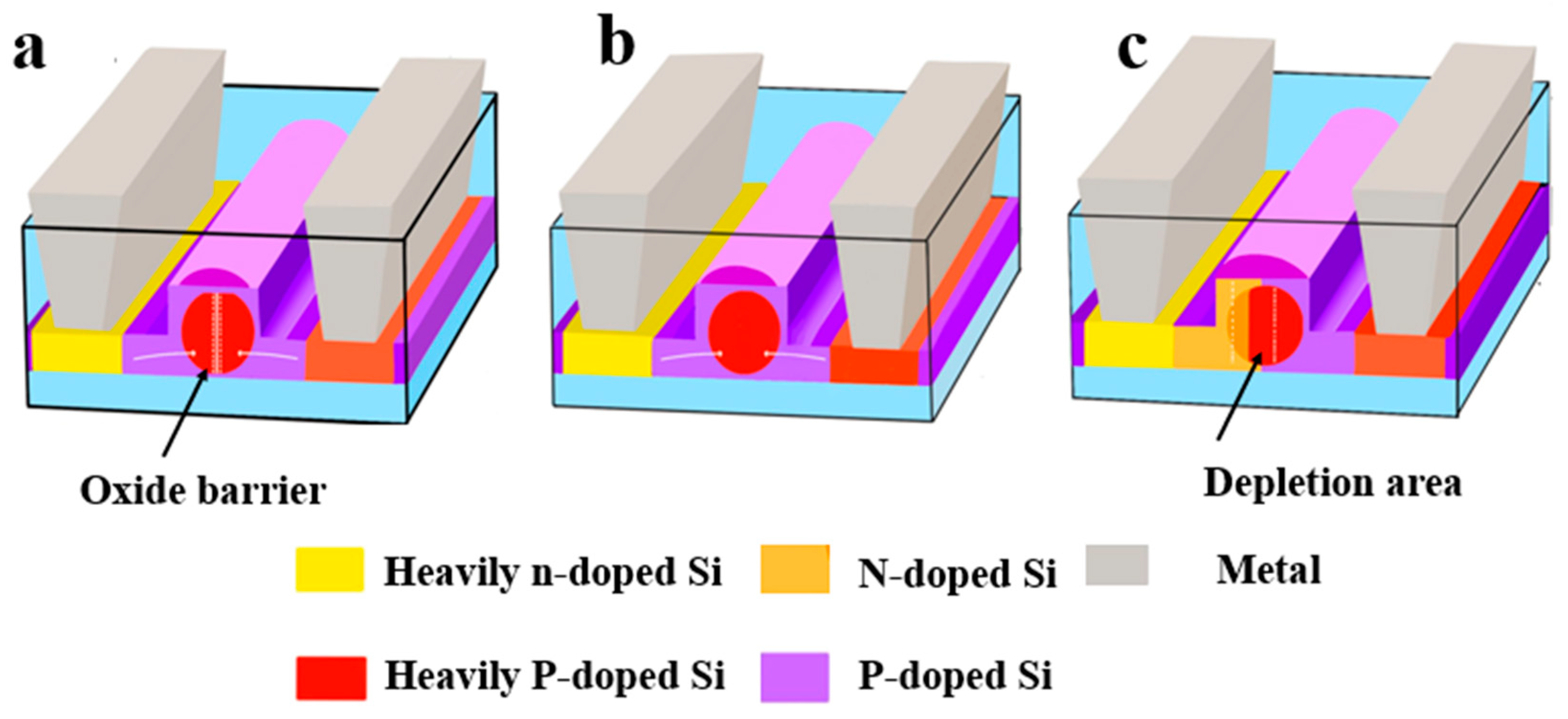
2.1. Silicon’s Modulating Characteristics

Silicon modulators are important elements in silicon photonics due to their ability to adjust the intensity, phase, or polarization of light as it propagates in the silicon waveguide. The theoretical basis of silicon modulators lies in the interaction between photons and the material properties of silicon, which can dynamically change the properties of light within the device [15].
Fundamental Principles of Silicon Modulators:
  • Free-Carrier Dispersion Phenomenon: Electro-optic Effect
    • Compared to lithium niobate and various other materials, silicon exhibits limited electro-optical effects due to the free-carrier dispersion effect on its refractive index. This effect comes from an increase or decrease in carriers (electrons and holes), which changes the refractive index of silicon, as shown in the following equation:
      Δn (at 1550 nm) = −[8.8 × 10⁻²² × ΔN + 8.5× 10⁻¹⁸ × ΔP0.8]
      Δn (at 1310 nm) = −[6.2 × 10⁻²² × ΔN + 6 × 10⁻¹⁸ × ΔP0.8]
      The change in absorption is described by
      Δα (at 1550 nm) = 8.5 × 10⁻¹⁸ × ΔN + 6 × 10⁻¹⁸ × ΔP [cm−1]
      Δα (at 1310 nm) = 6 × 10⁻¹⁸ × ΔN + 4 × 10⁻¹ 8 × ΔP [cm−1]
      where ΔN and ΔP are the carrier densities of electrons and holes.
    • The change in refractive index affects the phase or amplitude of light passing through silicon, allowing interferometers to modify the phase or intensity.
    • Silicon waveguide p-n junctions utilize free-carrier dispersion. Applying a voltage across the junction enables the movement of carriers, thereby modifying the optical characteristics of the silicon waveguide.
2.
Plasma Dispersion Effect:
  • The plasma dispersion effect can change silicon’s absorbance and refractive index by altering the concentration of free carriers (electrons and holes).
  • Applying a forward or reverse bias across the p-n junction changes the number of silicon carriers. This changes the waveguide’s refractive index, the way it absorbs light, and how it moves.
3.
Carrier Injection, Depletion, and Accumulation:
  • Carrier injection: modulators introduce carriers into silicon waveguides through a forward-biased PN junction. Injection carriers alter the refractive index and absorption of the waveguide.
  • Carrier depletion: Modulators use a reverse-biased p-n junction to remove carriers from a silicon waveguide.
  • Carrier accumulation: When a voltage is applied across the silicon dioxide interface, it leads to the accumulation of carriers, which subsequently changes the refractive index.
Silicon modulators use the free-carrier plasma dispersion (FCD) effect to quickly change the structure of the SiPh platform, as shown in Figure 1.
Due to the inherent limitations of the free-carrier dispersion (FCD) effect, silicon lacks the fast and linear electro-optical response of materials such as lithium niobate. High-speed modulation requires the integration of alternative materials into silicon photonic (SiPh) platforms [15,16,17,18,19,20].
As SiPh technology moves toward commercialization, new modulation techniques must surpass FCD-based silicon modulators in speed and efficiency. Research on thin-film lithium niobate, organic electro-optic polymers, and plasma–organic hybrids is of great significance for achieving the high-speed and efficient modulation required for next-generation SiPh systems.

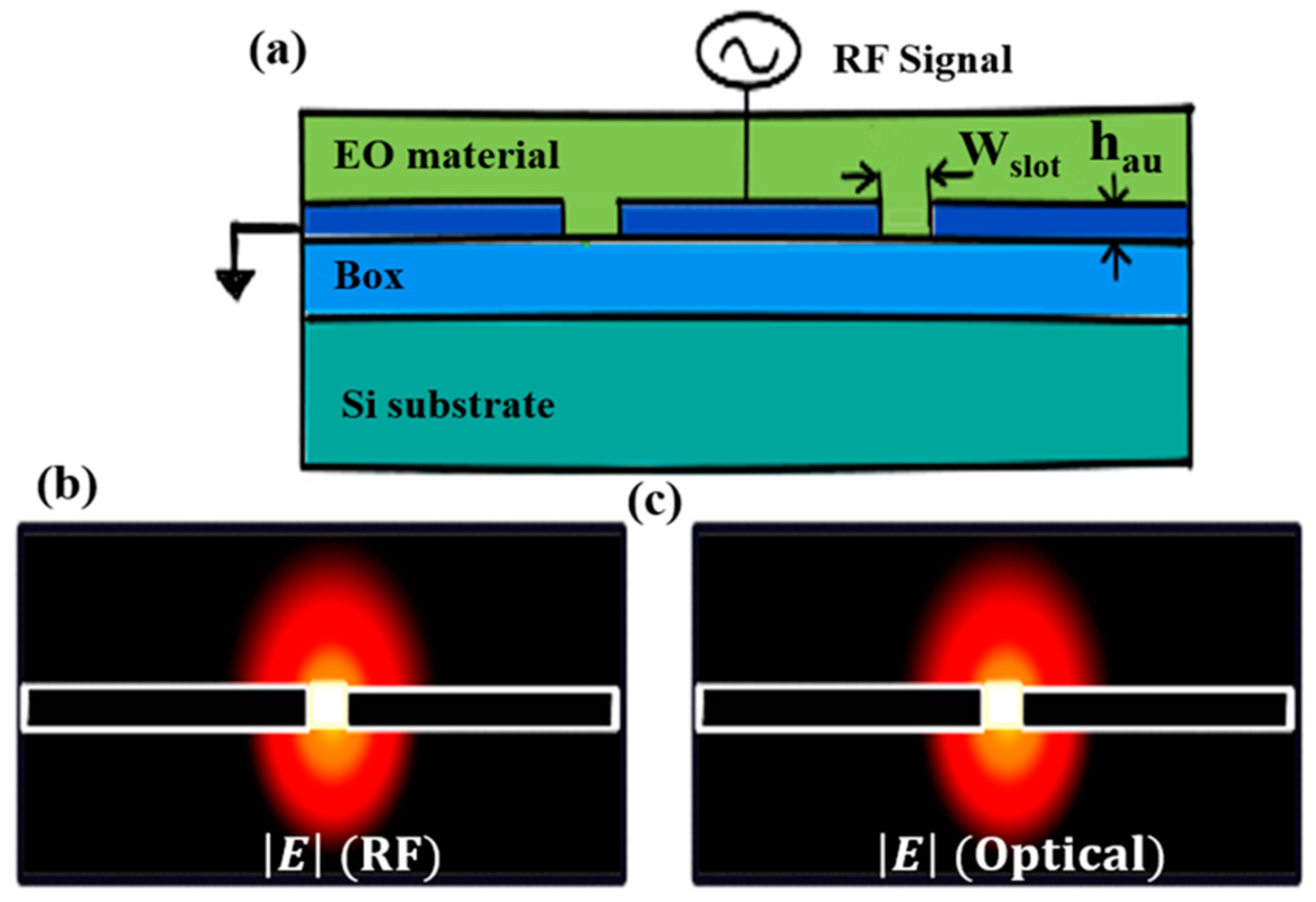
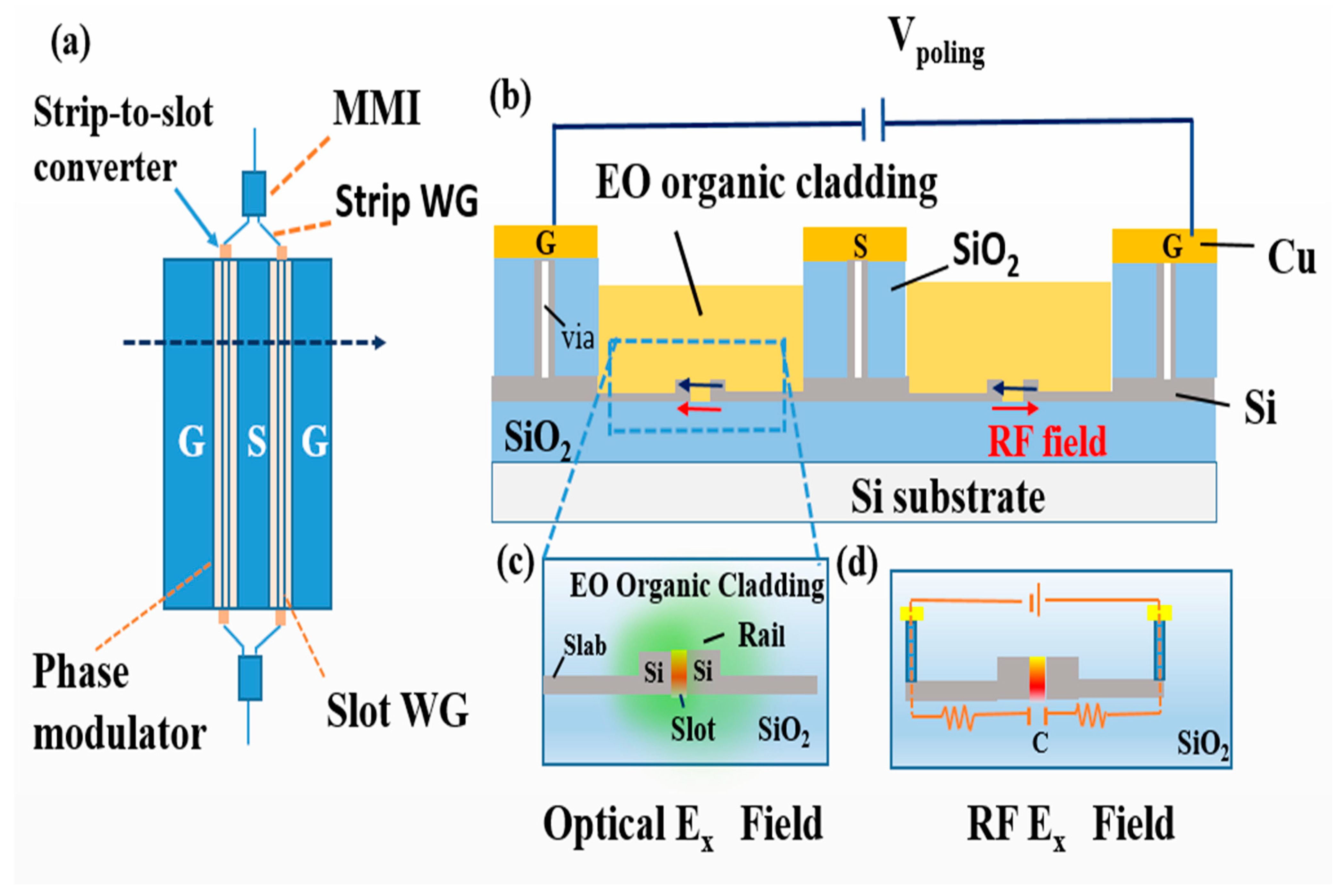
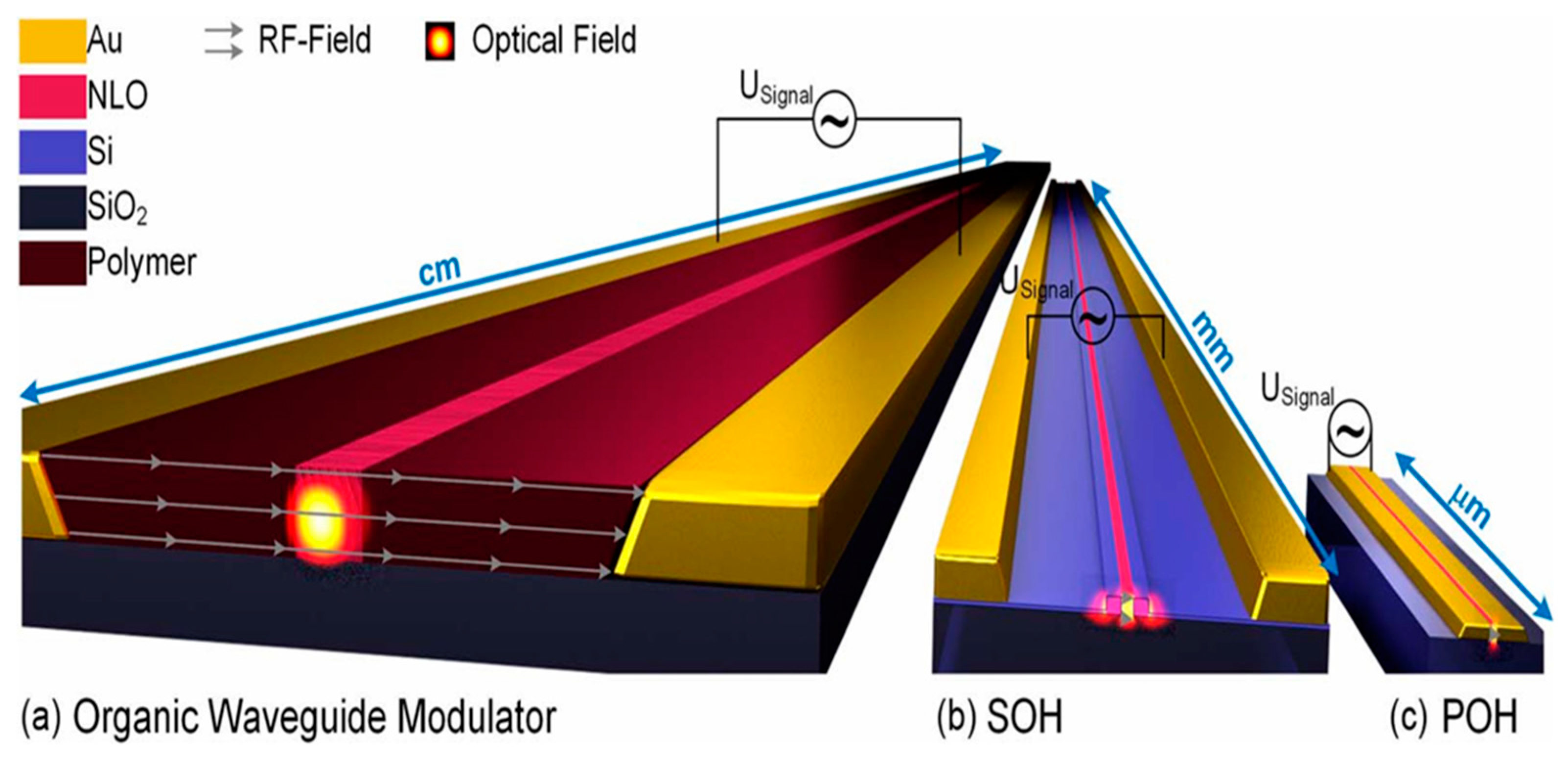
2.2. Overview of Technologies: TFLN/SOH/POH Modulator

The latest technologies used in optical communication systems include TFLN, SOH, and POH modulators, which have significantly improved optical signal modulation capabilities. The advantages and disadvantages of these technologies are evaluated below.

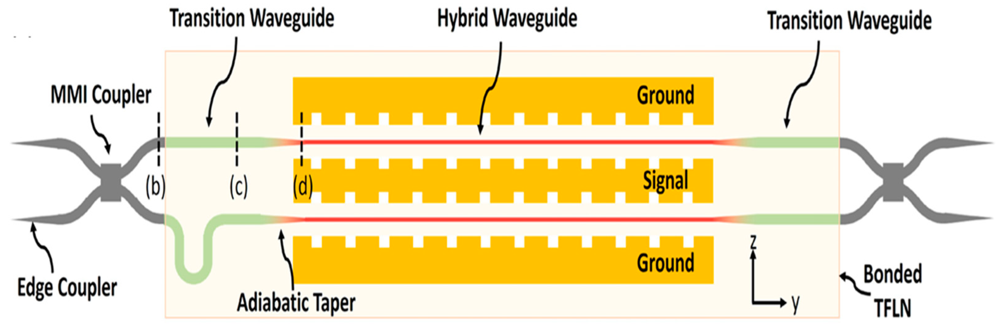
2.2.1. Thin-Film LiNbO3 Modulator Technology

Lithium niobate is an anisotropic material with the Pockels effect, which means that the refractive index changes linearly with the electric field. Material properties: The surface energy density in the field vector space is constant in the principal-axis coordinates. As shown in Figure 2, there is a principal refractive index for each orthogonal principal direction. The equation for the refractive index ellipsoid is as follows:
  ( 1 n 2 ) 1 x 2 + ( 1 n 2 ) 2 y 2 + ( 1 n 2 ) 3 z 2 + 2 ( 1 n 2 ) 4 y z + 2 ( 1 n 2 ) 5 x z + 2 ( 1 n 2 ) 6 x y = 1
where ( 1 n 2 ) i is the optical indicatrix. Upon the application of an electric field, the optical indicatrix changes as follows:
( 1 n 2 ) i = j r i j k E j
where Ej denotes the electric field, and rijk represents the linear electro-optic tensor. In an elliptical coordinate system defined by three axes, rijk is a 3 × 3 × 3 matrix, as illustrated below:
r i j = r 11 r 12 r 13 r 21 r 22 r 23 r 31 r 32 r 33 r 41 r 42 r 43 r 51 r 52 r 53 r 51 r 62 r 63
For particular Pockels crystals with specific point-group symmetry structures, the number of nonzero tensors can be further reduced. The linear electro-optic tensor matrix for LiNbO3 can be simplified to the following form:
r i j = 0 r 22 r 13 0 r 22 r 13 0 0 r 33 0 r 42 0 r 51 0 0 r 22 0 0
Table 1 shows that LiNbO3 has a maximum electro-optic coefficient of r33.
Figure 2 demonstrates that waveguide-based modulators achieve the best electro-optic coefficients when the electric field, E, aligns with the Z-axis and the light points in the same direction. Equation (5) simplifies the index ellipsoid with Ez as follows:
1 n x 2 + r 13 E z x 2 1 n y 2 + r 13 E z y 2 1 n z 2 r 33 E z z 2 = 1
We can obtain the following simplified Formulas (10) and (11) for LiNbO3’s index ellipse along the three axes by considering the small changes in the refractive index that occur when an electric field is applied:
n x   =   n y   =   n o   +   Δ n x     n o 1 2 n o 3 r 2 r 13 E z
n z = n e + Δ n z     n e 1 2 n o 3 r 2 r 13 E z
where ∆nx and ∆nz are the refractive changes upon the application of an electric field, Ez. For waveguide-based MZMs, the refractive index Equations (10) and (11) need to be supplemented by the waveguide effective index neff.
Bulk lithium niobate (LN) waveguides have insufficient optical confinement for millimeter-scale mode sizes and bending radii, making it difficult to realize effective micro-resonators, dispersion engineering, and dense integration in bulk LN [27].
TFLN addresses these issues by increasing the refractive index contrast to enhance optical confinement. This improvement can achieve better light focusing, higher uniformity, and lower packing density while retaining the excellent properties of LN.
Furthermore, these devices can be integrated with photonic platforms by exploiting the highly linear electro-optic modulation properties. For example, Figure 3 shows a waveguide-based Mach–Zehnder modulator (MZM) [28].
In these modulators, a voltage (V) is applied to the waveguide shifter, which creates a phase difference ∆ϕ between the arms of the LiNbO3 MZM, enabling precise modulation.
ϕ = 2 π λ Δ n eff L
where L represents the length of the phase shifter, while λ denotes the input wavelength.
V π L = d λ r Γ n e f f 3
where d is the parallel electrode distance. Equation (13) shows the MZM’s modulation efficiency, also called the half-wave voltage–length product (VπL).
Equation (13) shows that the modulation efficiency can be improved by modifying neff by adjusting the waveguide dimensions or by increasing the overlapping factor when fabricating the electrodes. The researchers developed several small, high-performance TFLN modulators with lossless waveguides and ultra-high bandwidths exceeding 110 GHz that can be fabricated using CMOS processes [28].
In order to produce high-quality TFLN, “Smart-Cut” technology is used to produce high-quality LN on thin-film insulator (LNOI) wafers to use in the TFLN-MZM.
Figure 4 shows the process of manufacturing an LNOI-MZM using Smart-Cut technology [29,30].
Given their excellent electro-optical properties, wide bandwidths, and low power consumption, TFLN modulators are key technologies for high-speed optical communication. However, several issues must be resolved to realize their full potential in practical applications. Some of the primary challenges in TFLN modulators include the following:
  • Fabrication Complexity: The highly complex bonding steps lead to non-uniform electro-optical performance and higher optical losses, which reduces production yields and makes the process more difficult to scale up.
  • Optical Loss: Even though lithium niobate is a low-loss material, it can cause optical losses and manufacturing flaws that lower the efficiency and performance of modulators used for long-distance communication and applications that need to save power.
  • Thermal Management: The refractive index of lithium niobate changes with temperature, which can affect the operation of TFLN modulators, especially in photonic circuits that are tightly mounted and cannot dissipate heat well. This results in phase drift and reduced efficiency.
  • Driving voltage and power consumption: LN modulators need high driving voltages to provide a large modulation depth. This makes it difficult to lower the voltage without affecting performance or power and presents a challenge for applications that require power conservation.
  • High-Frequency Operation: Due to the limitations of the electrode design and modulator signal transmission, high-frequency operation (e.g., above 100 GHz) with low loss and efficient modulation becomes difficult.
Manufacturing complexity, optical losses, poor compatibility with CMOS integration, thermal management issues, and cost constraints hinder the application of TFLN modulators. Solving these problems is crucial to realizing its potential and enabling its widespread application in high-speed optical communication networks.
Table 2 summarizes the recent developments in LiNbO3-based modulators over the past five years.
P. Weigel et al. [19] demonstrated a 5 mm long hybrid integrated MZM with a bandwidth of 106 GHz, a VπL product of 6.7 V·cm, and 81% of the light confined in the LiNbO3 layer. The same research team also improved velocity matching by using slow-wave electrodes, thereby reducing VπL and increasing the product voltage to 3.1 V·cm [28], as shown in Table 2.
A. Ahmed et al. [45] demonstrated a hybrid LiNbO3-SiN MZM with a Vπ below 1 V by extending the electro-optic interaction region to 2.4 cm and reducing the electrode gap between the ground and signal. X. Huang et al. utilized a Michelson interferometer (MI) with a double EO interaction length [43] and achieved excellent modulation efficiency with a VL as low as 1.06 V-cm for a 0.6 mm long MI modulator (MIM). However, propagation limits the device bandwidth to 40 GHz.
S. Nelan et al. [41] increased the EO interaction length from 6 mm to 10 mm by using a folded waveguide structure. A 180° bend was introduced to overcome the polarity reversal between the optical mode and the electric field. The design achieves a modulation efficiency of 4 V-cm and a bandwidth of 37.5 GHz.
P. Zhang et al. [42] demonstrated an EO MZM on a SiN-loaded LNOI platform with a coplanar waveguide design for push–pull modulation. The achieved bandwidth is 30 GHz, and the VπL is 2.18 V·cm.
X. Liu et al. [44] proposed a 10 mm long modulator with an estimated bandwidth of over 300 GHz and a modulation efficiency of 1.2 V·cm. LiNbO3 thin films were bonded onto quartz substrates using BCB with air-filled undercut regions to enhance the waveguide mode confinement.

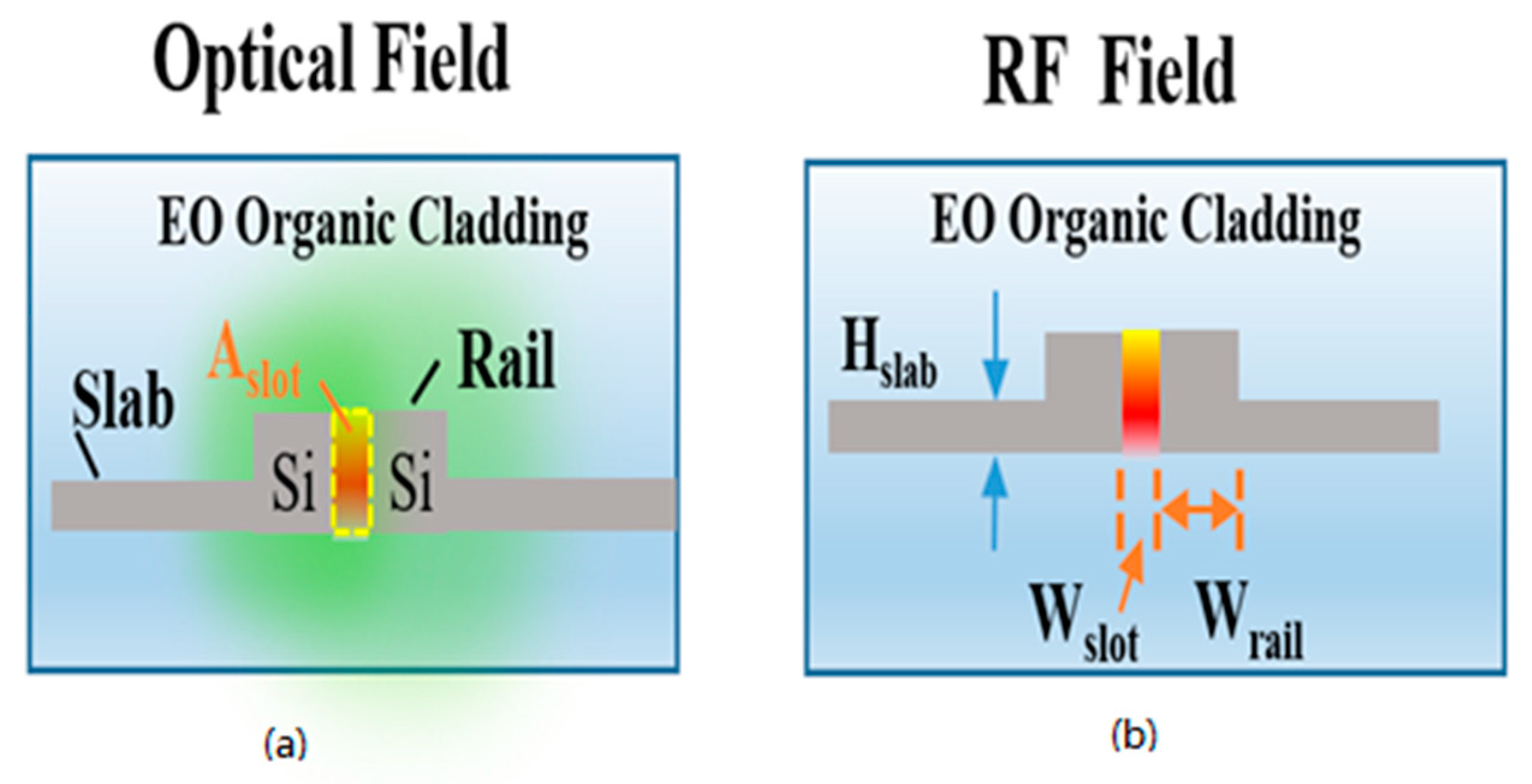
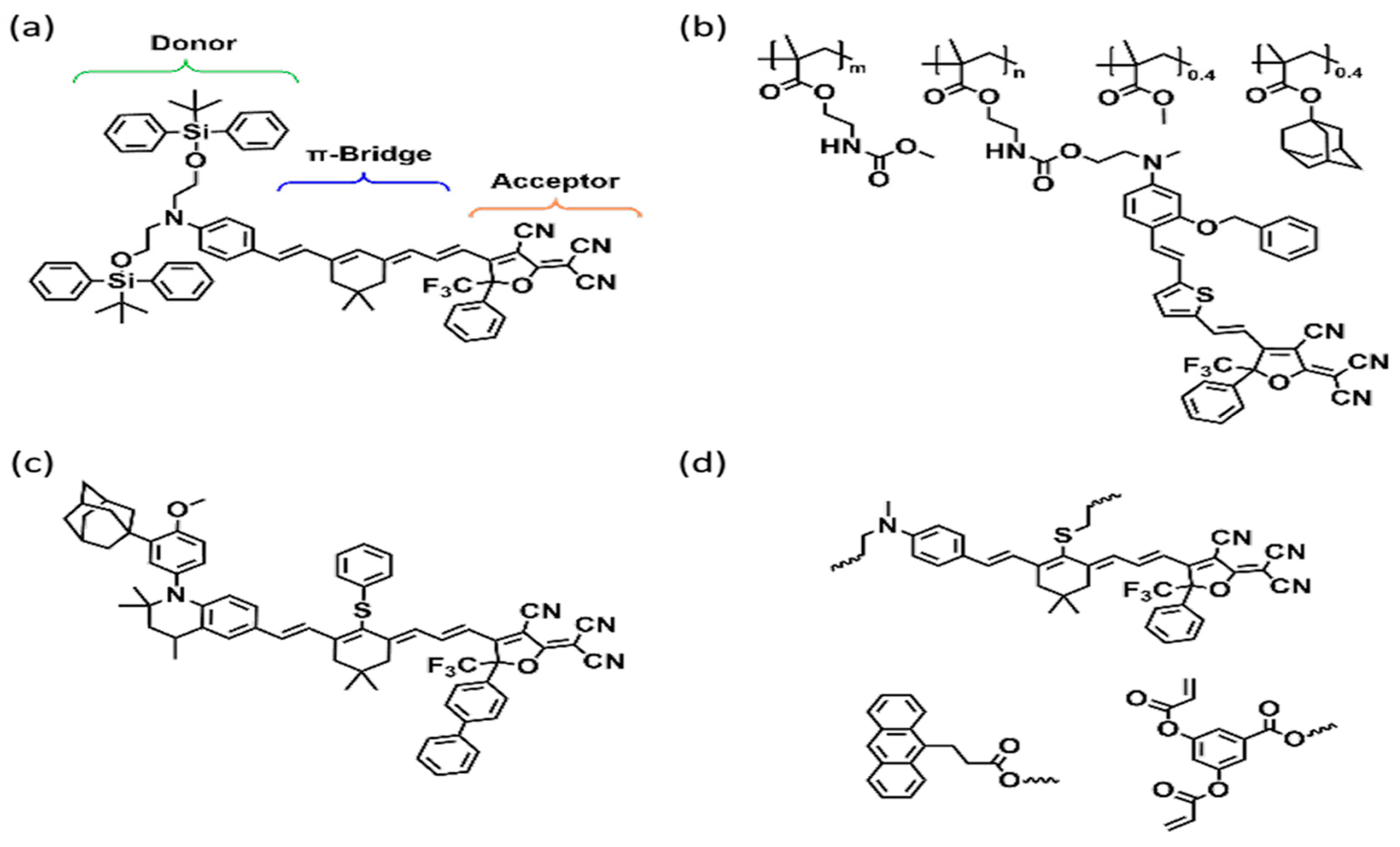
2.2.2. Silicon–Organic Hybrid Modulator Technology

Silicon–organic hybrid (SOH) modulators combine the optical properties of silicon photonics with the strong electro-optical responsiveness of organic materials.
Organic electro-optical (OEO) materials are characterized by high electro-optic coefficients, fast response speeds, and wide bandwidths [46]. The Pockels effect originates from the conjugated π-electron system of nonlinear optical molecules.
Combining Pockels-effect modulators, such as SOH [47,48,49] and plasma–organic hybrids (POH) [50,51], significantly improves the practicality of the device. The electro-optic coefficients of OEO materials are typically between 300 and 500 pm/V; however, theoretically predicted values exceed 1000 pm/V [52,53,54,55].
SOH integration combines the silicon photonic platform with organic electro-optical materials to form an optical phase modulator on a silicon substrate [56]. SOH modulators typically utilize organic electro-optical materials embedded in slotted waveguides. These materials exhibit χ(2) nonlinearity, enabling pure phase modulation without residual amplitude modulation [57].
The voltage–length product, VπL, highlights the significant bandwidth and modulation efficiency potential of the SOH modulator, which is more than 20 times better than conventional silicon modulators and comparable to InP modulators.
The slot in the optical waveguide is only 100 nm in size and is the core part of the SOH modulator. It can be manufactured using commercial optical lithography techniques, including 248 nm deep ultraviolet (DUV) technology [58]. Figure 5 shows the nine main steps of the SOH manufacturing process.
After preparing the waveguide and the electrode according to steps (1) to (8) in Figure 5, the slot is evenly filled with the organic EO polymer via spin coating, as shown in Figure 6.
SOH integration retains the compact dimensions and mature processing infrastructure of silicon photonics while incorporating the second-order nonlinearity of organic electro-optic materials for Pockels-effect-based electro-optic modulation.
The quasi-TE mode of the slot waveguide confines light within the slot area, Aslot [59]. The normal field component undergoes a discontinuity at the interface between the silicon rail and the electro-optic cladding material, resulting in field enhancement within the slot region. Figure 7a depicts the x-component of the optical mode, while Figure 7b provides an additional illustration of the x-component [60].
The phase shift Φ in a single SOH phase modulator is characterized by the field interaction, the refractive index n E O 1 of the electro-optic material, and the electro-optic coefficient, r33.
Φ = 1 2 n E O 3 r 33 E m Γ K o L
Equation (14) also incorporates the phase-shifter length L, the modulating field Em, and the vacuum wavenumber ko.
The SOH Mach–Zehnder modulator structure is shown in Figure 8a. The device consists of two SOH phase modulators operating in a push–pull configuration, controlled by a single coplanar transmission line arranged in a ground–signal–ground (GSG) layout. The cross-sectional view in Figure 8b highlights the slot waveguide of each phase modulator, which is coated with an organic electro-optic material. The primary optical quasi-TE mode is confined within the slot region, as shown in Figure 8c.
To facilitate modulation, thin n-doped silicon slabs electrically connect the transmission line’s metal electrodes to the rails of the phase modulators, ensuring a voltage drop across the narrow slot when a signal is applied. This design enables efficient modulation by generating a strong radio-frequency (RF) field, which is precisely aligned with the optical quasi-TE mode, as depicted in Figure 8d.
The π-voltages of a SOH Mach–Zehnder modulator and a singular SOH phase modulator can be expressed as Equation (15):
V π   = V π , MZM = w s l o t λ 2 n E O 3 r 33 Γ L
In addition to the slot waveguide, SOH modulators rely on organic electro-optic materials. These materials exhibit bandwidths spanning several tens of terahertz, with electro-optic coefficients (r33) measuring up to 500 pm/V [60]. Organic materials are particularly attractive for electro-optic modulators due to their ease of processing and compatibility with various material systems.
When organic electro-optical materials are applied to slot waveguides, the chromophores within these materials tend to exhibit unpredictable orientations. At the macroscopic level, achieving a stable and non-central orientation of the chromophores requires a specialized electric field poling technique. This technique ensures that the chromophores maintain the desired orientation over time despite their natural tendency to move nonlinearly. At high temperatures close to the glass-transition temperature, a poling voltage is applied to the floating ground electrode of the SOH Mach–Zehnder modulator to obtain the properties of the optoelectronic material, as shown in Figure 9. As a result, a poling field of approximately equal strength along the x-direction is generated in the two phase-shifter parts, as shown by the green arrows in the figure. The electric poling field exerts torque on the dipole chromophores, causing them to orient according to the poling field and produce an average eccentric orientation. While maintaining the poling voltage, the element is cooled to ambient temperature. Therefore, the chromophore arrangement remains unchanged even after the polarization voltage is removed. During the operation of the SOH MZM with GSG-structured electrodes, the modulation fields induced by the modulation voltage (or driving voltage), Um, in the two slot waveguides are in the same and opposite directions relative to the arrangement of the chromophores, as shown by the red arrows in Figure 9. Thus, the phase shifts in the two phase-modulator sections are equal in magnitude but opposite in sign, and the SOH MZM operates in push–pull mode [60].
The torque that the dipolar chromophores receive aligns them with the electric fields, resulting in an average acentric orientation. The poling voltage is maintained while cooling the device to ambient temperatures, and consequently, even after terminating the poling voltage, the alignment of the chromophores remains unaltered.
Organic electro-optic (OEO) materials:
Organic electro-optical materials comprise two primary components: polymers that alter the thermal and refractive indices and active chromophores responsible for electro-optical conversion [61]. Scientists are studying electronic and optical chromophores at the device level in order to create materials with greater r33 values (as shown in Figure 10), low optical loss, high thermal stability, and long-term alignment [62,63].
New progress in molecular engineering has improved the performance of chromophores in SOH modulators [64,65,66,67]. One example is JRD1 (Figure 11a).
The reorientation of molecular dipoles over time poses a challenge to the long-term stability of the material. To ensure stability, the temperature of the EO material and the Tg polymer matrix must be maintained above the operating temperature.
The conventional approach involves embedding NLO chromophores within polyacrylates or polycarbonates [66]. The host matrix increases their persistence by lowering electrostatic interactions and raising the glass-transition temperature (Tg = 150–200 °C). Polymers with very high Tg may not be the best choice for polarization due to the temperature at which thermally nonlinear optical (NLO) chromophores break down, as they require heating close to the glass-transition temperature (Tg).
The optical characteristics of the host, as well as the miscibility and solubility of polymers and chromophores in identical solvents or solvent combinations, must also be considered. In this method, NLO chromophores are bound to polymer or copolymer chains with methyl methacrylate (Figure 11b). Enhancing adamantyl moieties and optimizing copolymer designs elevate the Tg to 172 °C [67]. With a Tg of up to 176 °C (Figure 11c), NLO chromophores can covalently attach large adamantyl side groups [68].
Poling induces the thermal crosslinking of two NLO chromophores with complementary reactivity (Figure 11d). The cycloaddition of crosslinking units caused by heat creates a three-dimensional polymeric network that stops chromophores from moving and keeps the structure stable over time. The primary challenge in this approach is managing crosslinking during the poling process while maintaining the integrity of the chromophore scaffold [69].
  • Material Long-Term Stability: The slot in the optical waveguide is narrow, so the chromophores are exposed to extremely high light intensities, leading to lifetime limitations. Another factor is the lack of eccentric order between chromophores due to operating at the glass-transition temperature, Tg. Both effects improve the half-wave voltage Vπ.
  • Photochemical bleaching: When high optical intensities and oxygen are used in SOH devices, photochemical bleaching occurs. This breaks down electro-optic material permanently and raises the half-wave voltage Vπ [70].
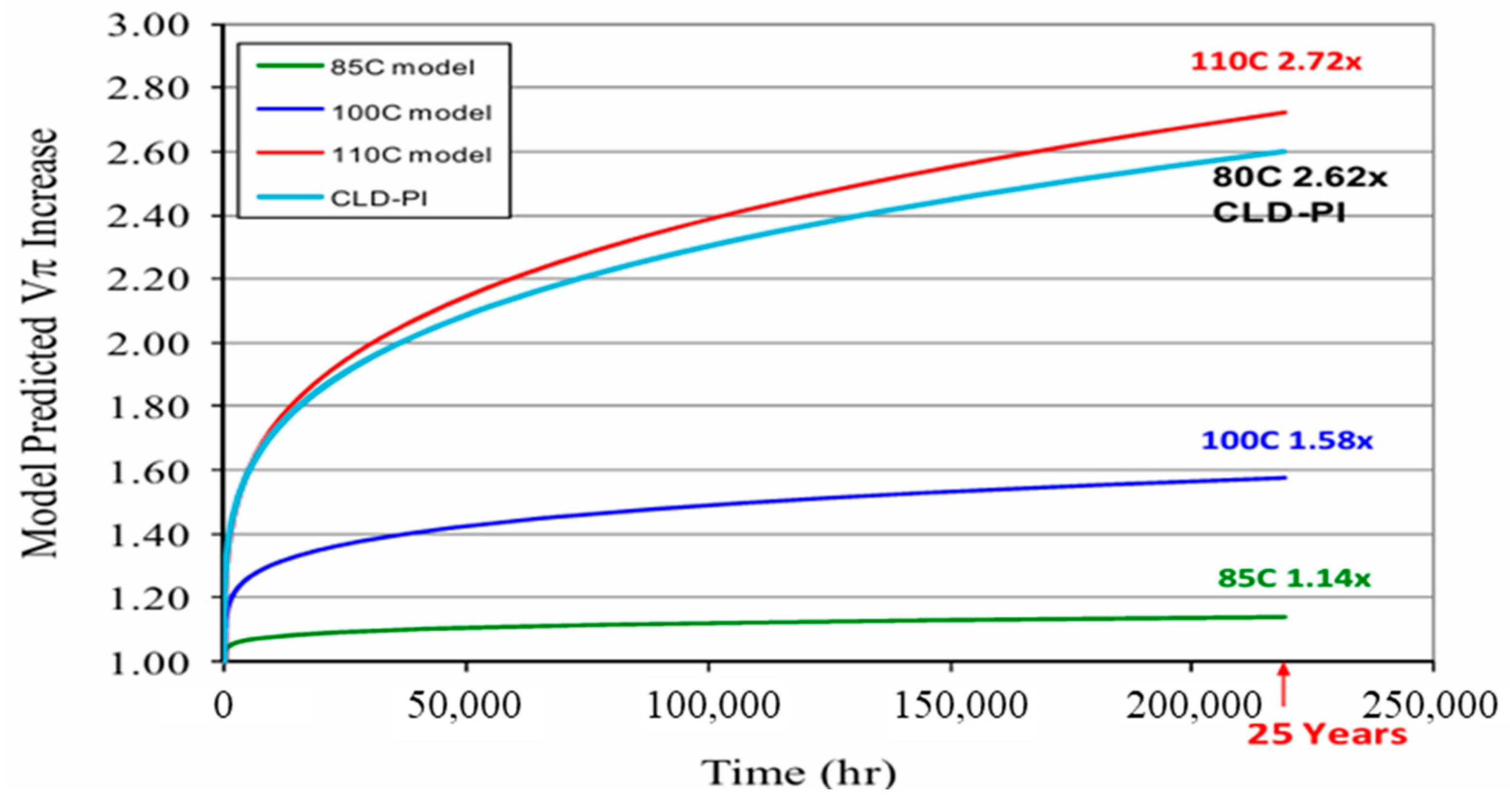
  • Thermal deploying: As the device’s operational temperature nears the Tg of the organic EO material, depolarization occurs, resulting in an increase in the half-wave voltage Vπ. Photonic devices are required to adhere to the Telcordia standard [71], which delineates reliability criteria. The designated maximum operational temperature according to this standard is 85 °C. Exceeding this temperature can lead to premature aging and performance degradation of the device.
Another method to enhance the thermal stability of EO materials is crosslinking, a procedure that necessitates the covalent bonding of two or more molecules. HLD constitutes a compound that comprises two molecules: HLD1 features an anthracene side group, while HLD2 incorporates an acrylic acid side group. The glass-transition temperature (Tg) of this material prior to crosslinking is 85 °C. The two complementary chromophore monomers, HLD1 and HLD2, undergo a thermally induced reaction to produce a resilient thermoset plastic, with the glass-transition temperature (Tg) rising by approximately 100 °C to 175 °C during the crosslinking process. Researchers employ HLD to obtain a more resilient material capable of enduring elevated temperatures without sacrificing performance, therefore enhancing the longevity and dependability of photonic applications [72].
HLD’s crosslinking process can maintain high EO activity (up to 300 pm/V at 1310 nm) while stabilizing the material, allowing it to withstand prolonged operation at elevated temperatures. In addition to in-device operation, the long-term storage stability of Sthin-film HLD EO devices at temperatures of 85 °C, 105 °C, and 120 °C was demonstrated in refs. [73,74].
Devices were poled in a thin-film configuration on a 20 nm PVD TiO2 charge-blocking layer, crosslinked to above 150 °C, and elevated by 10 °C every 10 min after reaching the poling temperature. The devices were stored in a N2-filled oven (which simulated a hermetic container), with n = 7 devices at 85 °C, n = 6 at 105 °C, and n = 5 at 120 °C.
Environmental stability testing is being conducted to determine packaging requirements. Figure 12 summarizes the stability statistics; all three conditions ensure long-term, steady functioning.
The schematic cross-section in Figure 13 displays numerous critical multi-project wafer (MPW) process flow components, including the SOH slot waveguide. The selective oxide aperture above the SOH modulator phase shifter is readily visible in this image. This enables the deposition of organic electro-optic material on the backside of the modulator, both within and around the slot. Electrical isolation between the silicon rails is crucial for electro-optic material poling and modulator performance. Currently, standard MPW services do not offer hybridization with an EO polymer; however, we anticipate this situation to change very soon [75].
Organic EO materials lack the Pockels effect due to the arbitrary orientation of the chromophores (Figure 14a). However, Figure 14b demonstrates that, during the poling phase, molecular dipoles achieve substantial r33 values [76,77]. Heating the material to its glass-transition temperature, Tg increases molecular mobility, while an applied voltage generates an electric field in the slot. This field aligns the molecules with the poling direction, as shown in Figure 14b. As the material cools, the molecular orientation is “frozen in” by the field, resulting in a stable alignment (Figure 14c). The electro-optic coefficient, r33, depends on the poling field strength, typically ranging between 200 and 400 V/μm. Surface–chromophore interactions create alignment effects along the slot walls, acting as a threshold mechanism.
At higher poling levels, r33 reaches a peak but subsequently declines due to dielectric breakdown and increased conductivity in the EO material. Reheating the material above a specific threshold temperature without an applied electric field in the slot can disrupt the chromophore alignment, reducing the r33 coefficient.
Typically, the electro-optic material is confined to slots narrower than 200 nm, with orientation effects primarily occurring near the silicon sidewalls [78]. Organic materials are also prone to environmental degradation from factors such as moisture, oxygen, ultraviolet light, and heat. To ensure the thermal stability of SOH devices, EO materials with high glass-transition temperatures—well above the device’s operational temperature—are required [79].
Application in Communications and Sensing:
The surge in data traffic from cloud services, video streaming, and AI has significantly increased the required capacity of optical communication networks, prompting research and development efforts to improve critical components. High-performance electro-optical modulators are crucial for power dissipation, compact module size, and cost efficiency, requiring a substantial bandwidth, a low drive voltage, and compatibility with CMOS processes [80].
Table 3 summarizes the results of recent experiments using SOH Mach–Zehnder modulators (MZMs) and IQ modulators. It highlights key metrics, including line speeds, modulation techniques, and drive voltages, demonstrating advancements in data transmission performance.
Table 3 also shows some of the most important device parameters, namely, the half-wave voltage–length product VπL, the device length L, the optical insertion loss per unit length of the modulator section α, and the combined half-wave voltage-loss product VπLα. Furthermore, the EO materials used are listed along with their glass-transition temperatures, Tg.
Wolf et al. [81] achieved a line rate of 400 Gbit/s using the 16QAM format using the SOH IQ modulator, which is the highest line rate published so far using the SOH modulator.
Eschenbaum et al. [77] achieved 280 Gbit/s and 150 Gbit/s using PAM4 and OOK signaling, respectively, with a peak-to-peak drive voltage of less than 1 V. It is noteworthy that the thermally stable organic EO material (PerkinamineTM) used has a glass-transition temperature exceeding 175 °C. After 900 h of thermal stress at 85 °C, the modulator did not show any performance degradation.
Kieninger et al. [82] demonstrated ultra-high EO activity in an RC SOH MZM with a half-wave voltage product of VπL = 0.32 Vmm. OOK data rates of up to 40 Gbit/s were achieved on a 1.5 mm long device at a record-low 40 mV peak-to-peak drive voltage. Leveraging the efficiency of SOH technology, 16 QAM signals can be generated and transmitted without amplifiers.
A strip waveguide-based variant of the SOH Mach–Zehnder modulator, also known as the SPH modulator, has been shown to achieve a high PAM4 line rate of 200 Gbit/s, although its UπL product is approximately an order of magnitude larger than that of its SOH counterpart [83]. Thanks to the device concept, optical losses are very low and are mainly caused by material absorption, resulting in a record-low half-wave voltage-loss product of 3.2 V dB.
The thermal behavior of the SPH modulator [84] was tested, and the results showed stable operation at temperatures of up to 110 °C. SPH devices have also been used in combination with other ultra-high- Tg materials, such as the device in [85], which achieved an OOK line rate of 110 Gbit/s in combination with an EO material with Tg = 185 °C.
SOH modulators, which combine the strengths of silicon photonics and organic electro-optical materials, enable high-speed, low-power optical modulation. This capability is critical for the development of future communication systems. These advancements have the potential to significantly improve the efficiency of data transmission and processing, thereby enhancing the performance of emerging technologies such as quantum computing and advanced imaging systems.
Table 3. Summary of performance metrics of SOH Mach–Zehnder and IQ modulators (table adapted from [65] under CC-BY 4.0).
DeviceLine Rate (Gb/s, Overhead)Modulation SchemeDrive Voltage (Vpp)VπL
(Vmm)
Device Length
(L, mm)
α [dB/mm]VπLα
(VdB)
EO
Material
Tg [°C]Ref.
Slot-WG-IQ-MZM400 (20%)16QAM1.510.6--SEO250130 [81]
Slot-WG-MZM280 (20%)
150 (7%)
PAM4
OOK
0.86
0.82
0.46
0.75
-
-
PerkinamineTM
Series 5A
>175[77]
Strip-WG-MZM200 (-)
110 (-)
PAM4
OOK
-14.480.223.2Synthesized Based on 172[83,84]
Strip-WG-MZM110 (-)PAM41.622-0.223.6EO194185[85]
Slot-WGIQ-MZM52 (7%)16QAM0.410.81.5--EO100140[86]
Strip-WG-MZM40 (-)OOK0.140.321.59.37.4JRD182[82]
Strip-WG-MZM (Si/InP hybrid)252 (-)PAM4--1.53.9-Synthesized Based on 172[87]
Slot-WG-CC-SOH MZM220 (20%)PAM411.31--YLD12481[88]

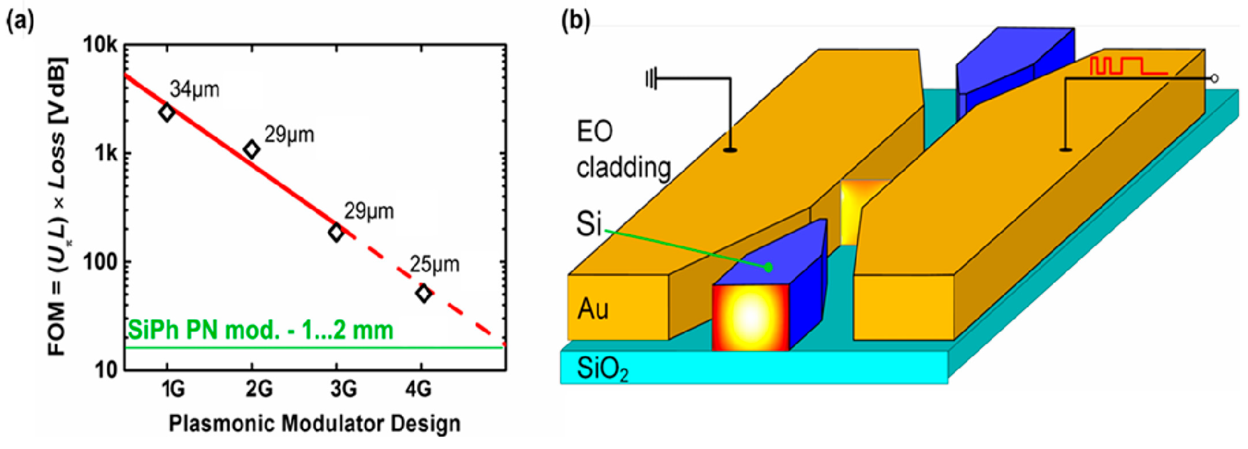
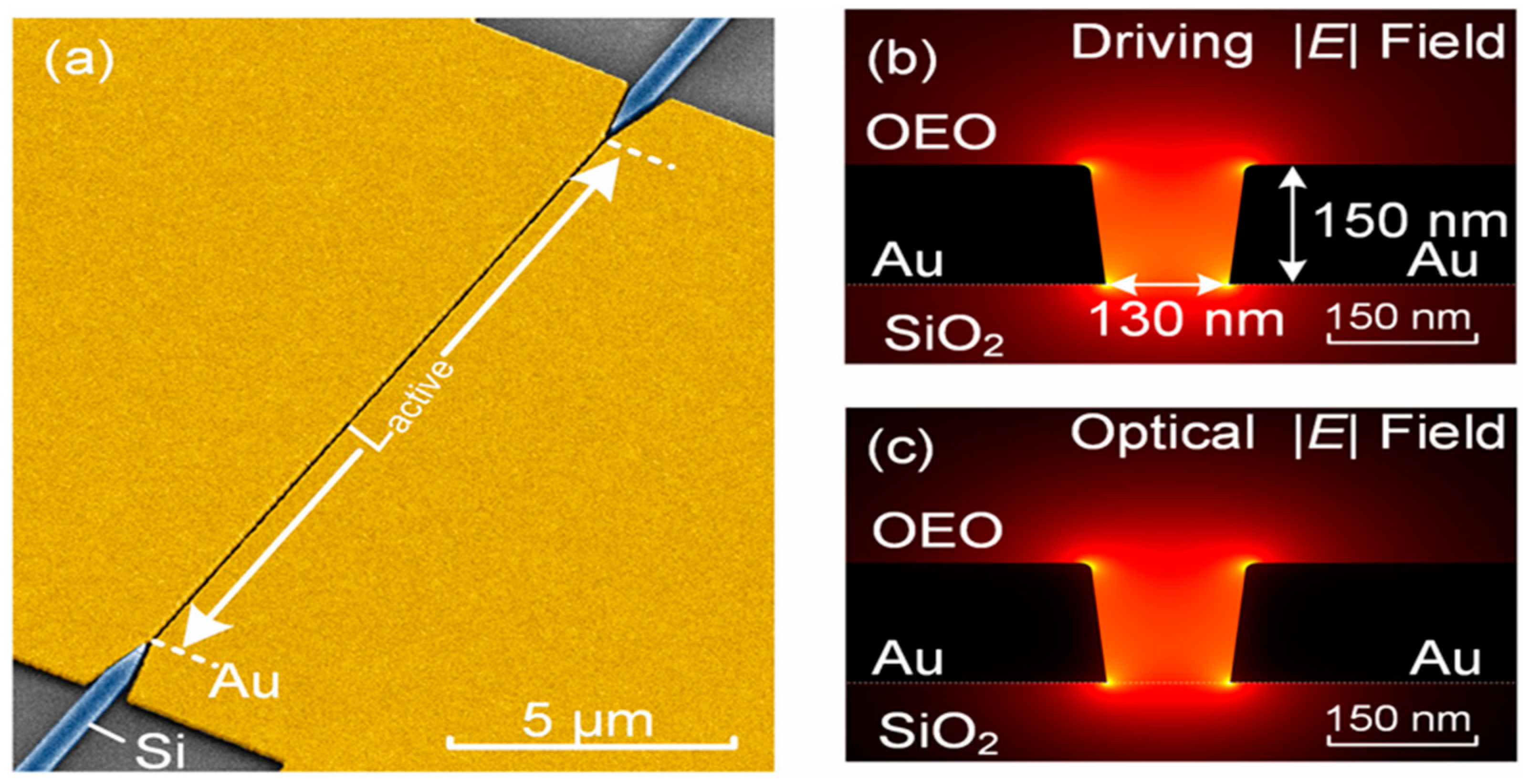
2.2.3. Plasma–Organic Hybrid Electro-Optic Modulator Technology

Plasma–organic hybrid (POH) electro-optic modulators combine plasmonics and organic materials to enhance performance, achieving higher speeds and greater energy efficiency. Plasmonics, the study of the interaction of light with free electrons in metals, enables the creation of ultra-compact photonic devices. Due to the diffraction limit, the mode size of a conventional dielectric waveguide cannot be smaller than half its wavelength. This limitation highlights the need for smaller components in nanoscale optoelectronic integrated circuits.
Surface plasma photonics offers a promising approach to developing ultra-compact, high-speed components. The modulator utilizes gold contact electrodes to directly form a metal–insulator–metal (MIM) slot waveguide.
In the POH phase shifter, a narrow metal strip guides light and radio-frequency (RF) signals, forming a metal slot waveguide that supports light propagation in the surface plasma polariton (SPP) mode.
Figure 15 shows a plasma slot waveguide with metal electrodes extending infinitely in the z- and y-directions, with the coupling of two metal–insulator interfaces, each supporting an SPP mode, giving rise to plasma slot modes [89,90]. Each metal–insulator interface supports an SPP mode, and when two interfaces are brought close together, the SPP modes couple to generate a plasma slot mode. The coupling of the two SPP modes gives rise to two solutions, namely, the symmetric and antisymmetric modes that propagate along the MIM slots.
The Ex field of the plasma slot mode is shown in blue. In the symmetric case, the electric field is strongly confined within the dielectric slot. The field in the metal decays exponentially in the y-direction, while the mode propagates in the z-direction. The Ex field of the antisymmetric solution changes sign in the dielectric tank. At telecommunication wavelengths and technologically relevant slot widths, the antisymmetric mode is below its cutoff frequency [91].
Organic Electro-Optic Materials:
Since the electro-optic coefficient of organic electro-optical materials is large, the electric field can significantly change their refractive index. These materials can respond quickly to electrical stimuli, which helps to swiftly modify optical signals. The stability and reliability of OEO devices depend largely on the stability of the material r33, which can be broken down into two different components: the first factor involves the chemical stability of the OEO material, and the second factor involves the orientational stability of the eccentric arrangement of the dipole chromophores that make up the OEO material.
The r33 of OEO materials can be described by the following formula:
r33 = βzzz ρN <cos3θ> G
where βzzz is the molecular hyperpolarizability, describing the nonlinear activity of a single chromophore; ρN is the number density of the chromophore; <cos3θ> describes the degree of eccentric arrangement of the chromophore; and G describes the local field factor.
Any chemical degradation of the chromophore will reduce the effective ρN of the active species. When first prepared, thin films of OEO material are initially isotropic, so <cos3θ> and r33 are zero. To align the chromophores, the OEO material is electrically polarized by heating it under a large electric field (~100 V/µm) to its glass-transition temperature (Tg), at which point the strongly dipolar chromophores can reorient in response to the external field, yielding a nonzero <cos3θ> and thus r33. The material is then cooled below Tg to lock the sequence in place before the field is removed.
However, without the polarization field, any subsequent local molecular motion would be driven toward the centrosymmetric alignment by the strong chromophore dipole–dipole interactions and result in losses in <cos3θ> and r33. Therefore, the OEO material must be protected after poling to prevent its temperature from approaching Tg. A promising approach to addressing this problem is to utilize lattice-hardening crosslinking reactions to significantly increase Tg during or after poling. POH design can also achieve local encapsulation of encapsulation layers to prevent chemical degradation through the selective area deposition of appropriate OEO materials. This approach has proven to be cheaper than traditional hermetic packaging.
POH Modulator Structure:
An organic electro-optic substance is integrated with a plasmonic waveguide in POH modulators. A metal, such as gold or silver, generally constitutes the plasmonic waveguide, with the organic material situated near the plasmonic mode. As shown in Figure 16, the structure tightly confines the electromagnetic field, which strengthens the interaction with the organic material [92].
Figure 17 illustrates the size variation among different organic-based hybrid modulators, including all-organic SOH and POH modulators. All-organic thin-film optoelectronic oscillator (OEO) devices consist of a core OEO layer, a lower cladding layer, and an upper cladding layer, all of which are composed of polymeric materials.
The three layers are positioned between the top and bottom electrodes. To achieve a low half-wave voltage, devices typically require lengths of 1–2 cm, as electrode separations exceeding 7 μm (the combined thickness of the three-layer films) are necessary [94].
The SOH modulator in Figure 17 reduces the electric field within the silicon slot waveguide embedded with OEO materials. This configuration enables significant overlap between the optical and RF electric fields, thereby shortening the device length to several hundred micrometers.
The POH modulator, on the other hand, utilizes metal slot waveguides instead of silicon, resulting in enhanced light-field confinement for the SPP. This design further reduces device lengths to several tens of micrometers and decreases electrode spacing to less than 50 nm. As shown in Figure 18, for a 2 V CMOS drive, the phase-shifter lengths for lithium niobate and silicon PN junction modulators are 1 cm and 2 mm, respectively, while the lengths for SOH and POH modulators are 200 μm and 25 μm, respectively [94].
The principles of the operation and bandwidth of POH modulators:
Plasma waveguides are critical components of POH modulators. These waveguides are typically constructed using a metallic layer, such as silver or gold, combined with a dielectric material. SPPs enable the confinement of light to sub-wavelength dimensions, focusing the electromagnetic field into areas significantly smaller than those achievable with conventional photonic waveguides.
This tight confinement is essential for enhancing the interaction between the light field and the organic electro-optic material, thereby improving modulation efficiency. The POH modulator integrates plasma metal–insulator–metal (MIM) slot waveguides with light-responsive organic electro-optic (EO) materials. Figure 19a illustrates the cross-section of a POH Mach–Zehnder modulator (MZM) fabricated on an SOI platform.
The MZM includes a phase modulator in each arm of its configuration. Each arm features a narrow metallic slit, 75–100 nm in width, positioned between gold electrodes (150 nm in height). The slots are filled with organic electro-optic materials.
The gold electrodes are driven by a modulating RF signal, which is predominantly confined across the metal slot (Figure 19b). The plasma slot also tightly confines the optical mode. As shown in Figure 19c, there is a significant overlap between the optical and RF electric fields, further enhancing modulation efficiency [95].
Figure 19. A POH modulator. (a) The cross-section of a POH Mach–Zehnder. (b) The plasma slot confines the electric-field profile of the RF modulation field. (c) The symmetric optical mode propagates through the plasma slot waveguide (figure reproduced from [96] under CC-BY SA 4.0).
Photonics 12 00429 g019
SPPs exhibit high transmission losses in plasma slot waveguides, leading to significant insertion losses in POH devices. For instance, a 75 nm wide slot (0.8 dB/µm) separating 150 nm gold layers in a 20 µm POH modulator results in a total insertion loss of approximately 16 dB [78].
The only RF bandwidth limitation for POH modulators is the RC cutoff frequency. Since POH devices are shorter than RF wavelengths, microwave loss and optical–microwave walk-off have a minimal impact on the bandwidth. Additionally, the highly conductive metal layers (with resistance approaching R→0) connecting the slot capacitance to the driving source enable POH devices to operate across a wide range of bandwidths. With a slot capacitance of only 3 fF, POH modulators can achieve RC cutoff frequencies exceeding 1 THz [97].
The novel POH phase modulator is depicted in the structural diagram in Figure 20. Light transitions from the silicon waveguide into the plasma waveguide, where it propagates in the SPP mode. The gap between the metal layers is filled with organic electro-optic (OEO) materials. When a voltage is applied to the metal electrodes, phase modulation is induced, leveraging the unique properties of the SPP mode.
Figure 21 depicts a scanning electron microscope image of the MZM component. A polymer known as DLD-164 fills the cavity, accounting for the device’s energy consumption of 25 fJ/bit and VπL of 0.06 V·mm [98].
The POH MZM combines silicon photonics technology with low-loss plasmonics to achieve ultra-light focusing, combined with highly efficient organic electro-optical (OEO) materials. This combination enables electro-optical modulation with bandwidths exceeding 500 GHz. Figure 22a shows a colorized scanning electron microscope (SEM) image of the POH phase modulator (PPM) [99,100].
The plasma slot waveguide consists of two gold electrodes with a narrow gap of about 130 nanometers in between, which is filled with OEO material. When an electrical signal is applied to the gold electrode, the electric field is concentrated on the nanoscale aperture (Figure 22b), thereby changing the refractive index of the OEO material. Light enters the plasma region through the silicon photonic waveguide and propagates along the metallic waveguide as surface plasma polaritons (SPPs).
The OEO material efficiently converts refractive index modulation into phase modulation by confining the light tightly within the slot (Figure 22c).
The HLD1/HLD2 organic materials used in the plasmonic modulator possess excellent electro-optical and thermal stability characteristics. A POH modulator fabricated with these organic materials can reliably sustain data modulation at temperatures exceeding 112 °C. Considering that the capacitance of the POH modulator is only a few femtofarads, its RC bandwidth is expected to exceed 1 THz, while the Pockels effect (caused by the recombination of electrons in nanoscale OEO molecules) occurs in femtoseconds or attoseconds. This suggests that the Pockels bandwidth may also be significantly greater than 1 THz.
Figure 23 shows the seven main steps of the POH-integrated EOM manufacturing process.
Table 4 provides a comparative analysis of various Mach–Zehnder (MZ)-type modulators, including photonic, plasmonic, and hybrid plasmonic variants. The table highlights the advantages of plasma electro-optic modulators.
Plasmonic electro-optic modulators exhibit several key advantages:
(a)
Significantly enhanced modulation efficiency, resulting in reduced VπL values.
(b)
Compact dimensions with cross-sections smaller than a wavelength.
(c)
Unmatched frequency and bandwidth capabilities compared to existing modulation techniques.
While plasmonic modulators do experience increased losses, the maximum penalty is typically limited to 3 dB. Recent hybrid plasmonic modulators achieve losses comparable to previous methods while maintaining significant bandwidths. These modulators exhibit remarkable compactness, flat frequency responses, bandwidths exceeding 500 GHz, reliable operation, thermal resilience and stability, and exceptionally low power consumption.

3. Comparative Analysis of Three Modulators: TFLN, SOH, and POH

Silicon photonic modulation is achieved using a variety of techniques, including TFLN, SOH, and POH modulators. Each technology has its own unique properties and advantages.
There are three main topics for discussion.
Modulation Efficiency:
The efficiency of the modulator at a specific wavelength λ (also known as the detuning factor) is given by VπL = λ/2Sp, where Vπ is the voltage required to introduce a phase shift of π, and L is the RF electrode length [107].
V π L = λ W s l o t 2 n 3 γ 33 Γ = λ 2 s p  
s p = n e f f V i n = 1 2 n 3 r 33 Γ d  
where Sp is the modulation sensitivity, defined as the change in the effective mode index with applied voltage; n is the refractive index of the EOP material in the slot; r33 is the electro-optic (EO) tensor coefficient of the material; Γ is the field overlap integral between the electric and optical fields [108]; and d is the distance between the two electrodes to which the modulation signal is applied.
To maximize Sp and thereby minimize VπL, both the material (i.e., n and r33) and the device structure (i.e., d and Γ) should be designed simultaneously. The EOP has a very large EO coefficient (i.e., r33). The r33 value of the crosslinked polymer is as high as 460 pm/V [69], while that of LiNbO3 is only ∼30 pm/V. A more comprehensive way to formulate the modulator efficiency is the loss efficiency, α × VπL (in V·dB), where α is the loss per unit length (in dB/mm).
Modulator bandwidth:
The bandwidth of the modulator depends on the speed match between RF and optical signals. The BW constraint is given by (BW × L)max ≈ 1.9c/π|nRF − no|, where c is the speed of light in a vacuum, nRF is the RF effective refractive index of the electrode, and no is the optical effective refractive index of the waveguide with the EOP [109]. Unlike LiNbO3, EOP waveguides can be optimized through different geometries and materials to closely match nRF. Therefore, low dielectric constant dispersion and a small velocity mismatch can lead to a large EOP modulator bandwidth exceeding 100 GHz [110]. For a TWE MZM, two other factors also limit the bandwidth: (1) the mismatch between the driver impedance, the characteristic impedance of the modulator electrode, and the terminal impedance, and (2) RF attenuation. Since the EOP MZM can be made smaller, it can be driven as a lumped-element device, achieving a larger bandwidth. Table 4 shows the BWs achieved by various EOP modulators, which are mainly limited by the RC time constant.
Energy consumption:
The total energy consumed by the modulator depends on several factors: static power consumption, dynamic power consumption, and optical IL. Static power consumption depends on the modulator structure and carrier dynamics.
Due to its excellent modulation efficiency, the EOP MZM can be made with L small enough to be driven as a lumped-element device. Compared to FCD MZMs, the static power of EOP MZMs can be significantly reduced. The carrier dynamics involved in this phase-shifting mechanism determine the operating current of the modulator. Carrier-depletion FCD modulators and Pockels-based modulators (such as LiNbO3 and SOH) do not consume significant bias current. In the case of an EOP, the dynamic power (proportional to CV2 pp) at a given frequency is also smaller, not only because of the lower peak-to-peak voltage swing (Vpp) requirement (from the lower Vπ) but also due to the reduced capacitance.
Higher α and longer L result in a larger IL of the regulator. As lasers are very inefficient and their wall-plug efficiency is typically less than 10%, compact modulators with small IL are highly desirable. The SOH modulator also remains competitive in this regard, as shown in Table 5.
The following paragraphs discuss the differences in the characteristics of TFLN, SOH, and POH modulators listed in Table 4 and Table 5.

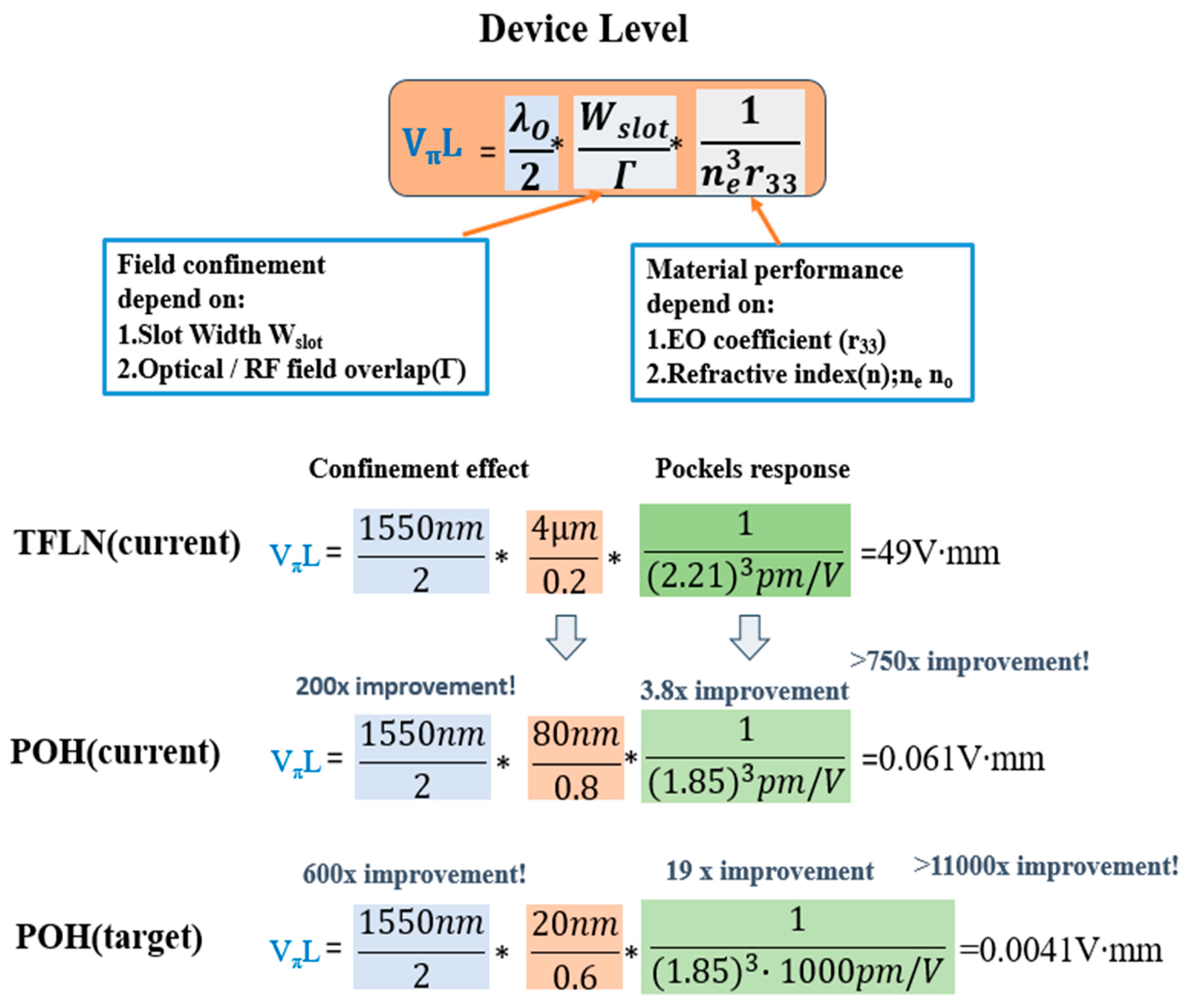
3.1. Modulation Efficiency

The VπL value is reduced mainly through the improvement of regulation efficiency. Among TFLN, SOH, and POH, POH has the lowest VπL value [113] and the highest regulation efficiency. VπL materials (i.e., n and r33) and device structures (i.e., d and Γ) should be designed as shown in Figure 24. The slot value of the POH optical waveguide is more precise from 80 nm to 20 nm, and the change in EO coefficient data can reduce the value of VπL.

3.2. Modulation Bandwidth

Unlike LiNbO3, where it is difficult to achieve high-frequency operation (e.g., over 100 GHz) with low loss and efficient modulation due to limitations in electrode design and modulator signal transmission, EOP waveguides can be optimized through different geometries and materials to closely match nRF. Therefore, lower dielectric constant dispersion and smaller velocity mismatch can lead to a larger bandwidth, over 100 GHz, in EOP modulators [64].
For TWE MZMs, two other factors also limit the bandwidth: due to the mismatch between (1) driver impedance, the characteristic impedance of modulator electrodes, and terminal impedance and (2) RF attenuation, the only RF bandwidth limitation of a POH modulator is the RC cutoff frequency. Since POH devices are shorter than the RF wavelength, microwave losses and optical–microwave walk-off have a minimal impact on the bandwidth. In addition, the highly conductive metal layer (resistance close to R→0) connecting the tank capacitor to the driving source enables the POH device to operate over a wide bandwidth. The POH modulator has a tank capacitance of only 3 fF and can achieve an RC cutoff frequency of over 1 THz [97]. Thus, in terms of bandwidth, the POH modulator has the best performance, followed by the SOH modulator and then the TFLN modulator.

3.3. Energy Consumption

Pockels-based modulators, such as LiNbO3 and SOH, do not consume significant bias current. The dynamic power (proportional to CV2pp) at a given frequency is also smaller for EOP, not only because of the lower peak-to-peak voltage swing (Vpp) requirement (from the lower Vπ) but also due to the reduced capacitance (in the slot-less structure). The loss efficiency VπLα is the best for all POH, followed by SOH and, finally, LiNO3.

3.4. Fabrication Complexity

Figure 4 shows that the process of manufacturing TFLN modulators is challenging because the bonding process is very complex, resulting in uneven electro-optical performance and higher optical losses, which reduces the yield and makes it more difficult to scale up. Figure 5 and Figure 23 are production flow charts for SOH/POH modulators. This workflow can be fully integrated into the CMOS process and backend process. Compared with the POH/TFLN process, SOH production is simpler, has a lower cost, and can be easily put into mass production.

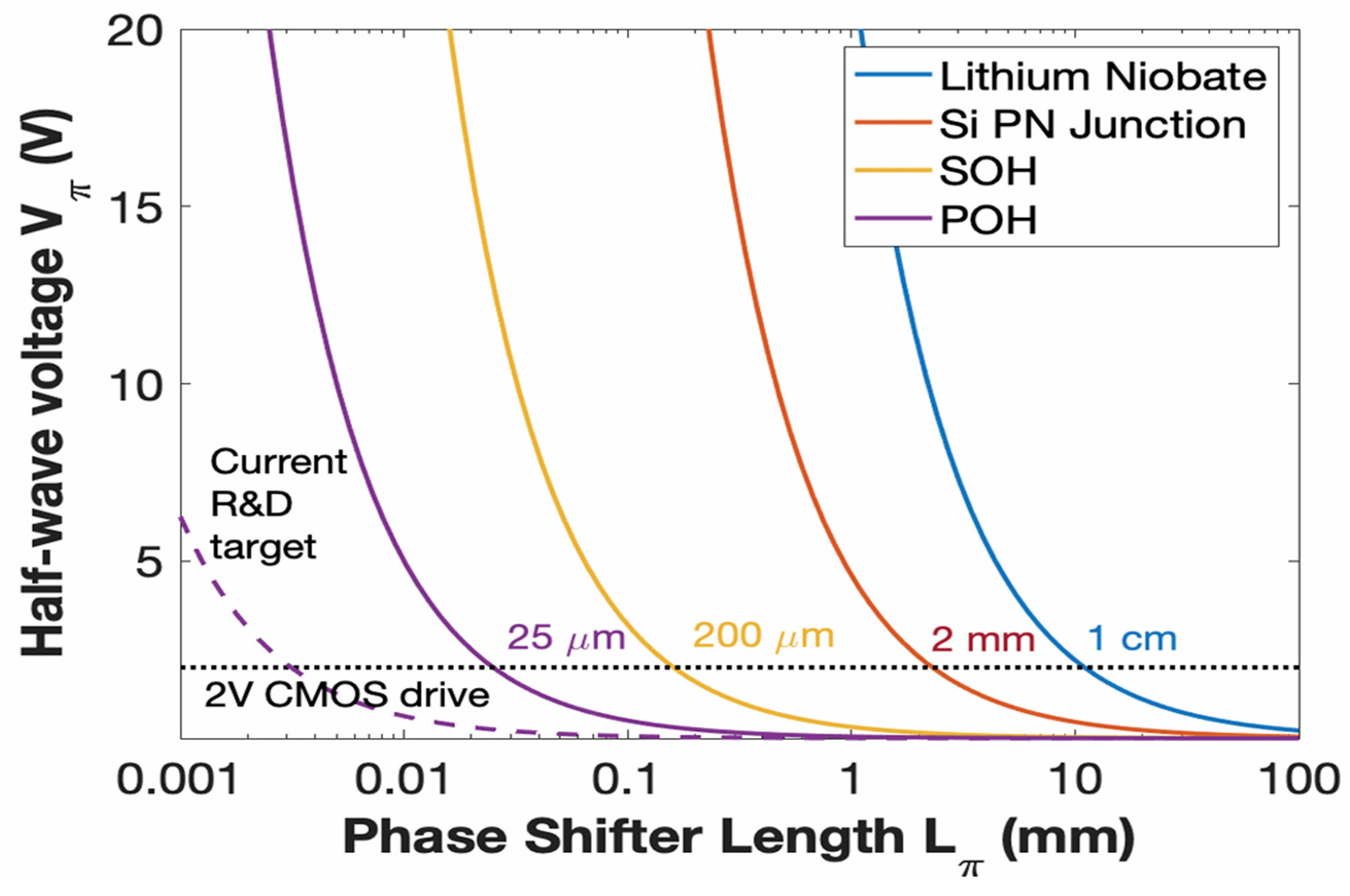
3.5. Footprint (Fixed Vπ)

For a 2 V CMOS drive, the phase-shifter lengths for LiNbO3 and SiPN modulators are 1 cm and 2 mm, respectively, while the lengths for SOH and POH modulators are 200 μm and 25 μm, respectively [94]. According to size, TFLN > SOH > POH. Since the TFLN structure is too long to integrate with precision optical modules (co-packaged optics), TFLN is suitable for traditional 800 G~1.6 T optical modules, and SOH is suitable for >1.6 T co-packaged optics modules. Since the POH structure reaches the nanometer level, it is easier to place in the chip, and the transmission distance is short, which is suitable for chip-to-chip transmission and used in optical I/O chip-to-chip applications.

3.6. Electro-Optic Coefficient, r33

The r33 value is closely related to VπL. As shown in Equation (17), r33 and VπL are inversely proportional.
V π L = λ W s l o t 2 n 3 γ 33 Γ = λ 2 s p
The larger the r33, the smaller the VπL and the higher the modulation efficiency. Organic electro-optical (OEO) materials are characterized by high electro-optic coefficients, fast response speeds, and wide bandwidths [46]. The electro-optic coefficients of OEO materials are typically between 300 and 500 pm/V; however, theoretical predictions have values exceeding 1000 pm/V [52,53], while the r33 value of LiNob3 is only 31 pm/v.

3.7. Temperature Stability

When the operating temperature of the SOH/POH device approaches the Tg of the organic electro-optical material, depolarization occurs, resulting in an increase in the half-wave voltage Vπ. According to Telcordia standards, the maximum operating temperature specified is 85 °C. Exceeding this temperature may cause premature aging and performance degradation of the device. Therefore, the SOH/POH must maintain optimal thermal management, which is critical for ensuring long-term stability and meeting Telcordia reliability requirements. However, the birefringence of LiNbO3 varies with temperature, but its temperature stability is higher than that of the SOH and POH.
Below is an overview of specific applications for thin-film lithium niobate (TFLN), silicon–organic hybrid (SOH), and plasma–organic hybrid (POH) modulators, highlighting their unique strengths and industry use cases.
  • Thin-Film Lithium Niobate (TFLN) Modulator
TFLN modulators are known for their ultra-low optical loss and high electro-optic performance, enabling high-speed, low-loss modulation. They use the Pockels effect for efficient phase modulation, unlike silicon-based modulators. TFLN supports bandwidths over 100 GHz with drive voltages as low as 1–2 V, making it ideal for advanced modulation formats like QAM. Key advantages include ultra-low optical propagation loss, high linearity, excellent thermal stability, and compatibility with hybrid integration.
  • Silicon–Organic Hybrid (SOH) Modulators
SOH modulators are recognized for their ultra-high-speed modulation, low drive voltage, and compact, CMOS-compatible design. These modulators use advanced organic electro-optic materials on silicon waveguides, enabling them to achieve modulation speeds over 100 GHz while needing less than one volt to operate. Key advantages include a compact footprint, direct compatibility with CMOS drivers, and CMOS-compatible fabrication processes. SOH modulators are a preferred choice for energy-efficient data center interconnects, chip-to-chip optical communication, and prototyping and R&D for advanced modulation formats and ultra-fast optics. They push the boundaries of modulation speed per unit length, making them ideal for systems where footprint, energy efficiency, and speed are critical.
  • Plasma–Organic Hybrid (POH) Modulators
POH modulators are renowned for their ultra-compact size, high bandwidth modulation, and low energy consumption, making them ideal for advanced data and RF applications. These modulators combine plasmonic waveguides with top-quality organic electro-optic materials, allowing them to modulate at speeds over 200 GHz in a very small space. The primary advantages include record-high bandwidths, ultra-low energy consumption per bit, a CMOS-compatible manufacturing process, and compatibility with ultra-dense photonic integration. POH modulators are well-suited for fast optical connections, high-frequency and THz photonics, fiber radio signal transmission, 5G/6G networks, and high-performance computing chip interconnections, thereby contributing to the development of the next generation of communication systems with exceptional bandwidth and rapid response.

4. Challenges, and Conclusions

Based on the plasma dispersion effect, continuous innovation in academia and industry around the world over the past 25 years has increased data rates by three orders of magnitude. Modulation speeds have increased from 100 Mb/s with non-return-to-zero (NRZ) formats to 224 Gb/s with four-level pulse amplitude modulation (PAM4) to over 300 Gb/s with eight-level pulse amplitude modulation (PAM8) [116,117] and, further, to 1 Tb/s with coherent dual polarization (DP)-64 quadrature amplitude modulation (QAM) [118].
The bottleneck for silicon modulators is that their bandwidth cannot keep up with the continued expansion of band rates to 200+ Gbaud in optical transceivers. Modulators all rely on the charging and discharging of capacitors, with current flowing through doped silicon, which cannot be too heavily doped in order to avoid excessive optical losses; meanwhile, inserting resistors will result in strong attenuation of the current or RF drive signal. Unfortunately, this is due to the fundamental material properties of silicon. As silicon does not exhibit the Pockels effect, its performance is limited by absorption and nonlinearities associated with plasmon dispersion effects.
Furthermore, speed is not the only concern for modulators; low power consumption and small size are also important factors. Data center designers need to reduce power consumption and optimize space efficiency as basic architectural standards. Integrating alternative materials into the SiPh platform, such as LiNbO3 and EO polymer, to form TFLN/SOH/POH modules can solve the bottleneck problem of silicon modulators [119]. Compare the differences between these three TFLN/SOH/POH modulator technologies from Table 6.
Despite the many benefits of SOH/POH, large-scale production remains a hurdle. Although the Tg of the EOP (EO polymer) in SOH/POH has been greatly improved, the low Tg remains a barrier for conventional SiP manufacturing procedures that require higher temperatures. When the temperature rises above Tg, the EOP loses its electro-optical characteristics. One approach is to move the polarization step to the final step of manufacturing to ensure that the EOP remains intact over the remaining process steps. However, as the final phase in manufacturing, the requirement for polarization and execution presents a barrier to existing manufacturing processes that must be addressed in order to accomplish mass production.
Another challenge is aging and long-term reliability. Figure 25 shows the model-predicted growth of Vπ over time for the EOP modulator described in [120] at different operating temperatures, showing its reliable operation for 25 years at 85 °C. Finally, it must be demonstrated that SOH modulators can operate for long periods of time without hermetic packaging, or low-cost hermetic packaging must be developed. A recent study [121] suggests that a modest barrier to water vapor transmission may be sufficient, rather than requiring a completely sealed enclosure.
The modulation efficiency and loss efficiency of the SOH modulator are improved by about 10 times compared with those of the FCD modulator, and the bandwidth is increased by about 2 times. However, there is a clear performance gap between SOH and POH modulators in terms of VπL and BW.
Improving the electro-optical and physical/chemical properties of the polymer and increasing r33 will further reduce the VπL of the SOH/POH modulator. The bandwidth of polymer modulators is usually limited due to the RC effect, so a lower VπL can achieve smaller devices and larger bandwidth. Improved device design and reduced EOP material losses can further reduce IL [94].
TFLN retains the excellent physical properties of LiNbO3, such as a wide transparency window, a large electro-optic coefficient (r33 = 31 pm/V), and a linear Pockels effect. Heterogeneous TFLN/silicon and TFLN/Si3N4 modulators are fabricated using chip-to-wafer bonding technology. Heterogeneous integration has demonstrated highly competitive performance, including a modulation efficiency of 2.2 V·cm, a bandwidth exceeding 110 GHz, and a modulation rate of up to 112 Gbit/s [111,122].
For monolithic TFLN modulators and PICs, 150 mm is the maximum size of wafers among current products. The wafer size is limited, the device footprint is large, material costs are relatively high, and film uniformity accounts for a large portion of the wafer cost. While wafer fabrication is not overly complex, achieving uniform waveguide formation for ultra-low-loss operation is not trivial and requires optimized lithography, etching techniques, and post-fabrication processes.
TFLN modulators heterogeneously integrated with silicon or Si3N4 are still in the R&D stage. Similar to III–V heterogeneous integration on silicon, TFLN integration occurs in the back end of the line (BEOL) and requires specialized processing tools as well as stringent cross-contamination controls, especially when large-scale wafer-scale processing is involved.
Furthermore, we need to reduce the length of TFLN MZI modulators to a few millimeters or sub-millimeters to be feasible and competitive in future co-packaged optics (CPOs). Modulators based on ring-assisted designs [123] and slow-light structures [124,125] have made LNs more efficient, achieving lengths of hundreds of microns, although this sometimes requires compromises in the operating wavelength or bandwidth. Therefore, future optimization to find the best balance between these quality factors is crucial.
TFLN, SOH, and POH modulators each have their own beneficial characteristics: TFLN has the smallest insertion loss, SOH is the easiest to integrate into the CMOS process, and POH has the largest bandwidth and the smallest footprint. Their application fields are also different. Below, we summarize the applications of these modulators.
TFLN modulators are best suited for long-distance, high-bandwidth applications such as telecommunications, microwave photonics, and quantum communication, where low insertion loss and high precision are critical.
SOH modulators are ideal for short- to medium-range, low-power, and high-speed applications such as data center optical links, 5G networks, and silicon photonics, offering a balance between performance, size, and energy efficiency.
POH modulators are highly effective in ultra-compact, high-speed, and low-power applications, especially in on-chip optical communication and photonic integrated circuits that prioritize space and energy efficiency.
The next generation of high-capacity, high-performance modulators will soon arrive. TFLN/SOH/POH modulators have demonstrated impressive performance. The superior r33, aging, reliability, manufacturing, and packaging of SOH/POH modulators, as well as further improvements in TFLN film thickness uniformity and design kit (PDK) demonstration, will enable their application in the next generation of silicon photonics.

Author Contributions

Conceptualization, T.-C.Y. and A.-C.L.; methodology, W.-T.H.; validation, C.-H.L.; investigation, T.-S.K. and C.-C.W.; resources, S.-W.C.; data curation, C.-W.S.; writing—original draft preparation, T.-C.Y.; writing—review and editing, A.-C.L.; visualization, H.-Y.L.; supervision, C.-W.C. and H.-C.K. All authors have read and agreed to the published version of the manuscript.

Funding

This research received no external funding.

Institutional Review Board Statement

National Science and Technology Council (NSTC 112-2221-E-002-176-MY3, NSTC 113-2119-M-002-023, NSTC 113-2640-E-005-001, NSTC 113-2221-E-002-101-MY3).

Informed Consent Statement

Not applicable.

Data Availability Statement

The data presented in this study are available from the corresponding author upon reasonable request.

Conflicts of Interest

Author Chang-Chin Wu was employed by the company Foxconn Technology Co., Chin-Wei Sher, Huang-Yu Lin and Hao-Chung Kuo were employed by the company Hon Hai Research Institute. The remaining authors declare that the research was conducted in the absence of any commercial or financial relationships that could be construed as a potential conflict of interest.

References

  1. Dai, D.; Bauters, J.; Bowers, J.E. Passive technologies for future large-scale photonic integrated circuits on silicon: Polarization handling, light non-reciprocity and loss reduction. Light Sci. Appl. 2012, 1, e1–e12. [Google Scholar] [CrossRef]
  2. Mu, X.; Wu, S.; Cheng, L.; Fu, H. Edge couplers in silicon photonic integrated circuits: A review. Appl. Sci. 2020, 10, 1538. [Google Scholar] [CrossRef]
  3. Rachel, W. Integrating silicon photonics. Nat. Photonics 2010, 4, 498–499. [Google Scholar]
  4. Shekhar, S.; Bogaerts, W.; Chrostowski, L.; Bowers, J.E.; Hochberg, M.; Soref, R.; Shastri, B.J. Roadmapping the next generation of silicon photonics. Nat. Commun. 2024, 15, 751. [Google Scholar] [CrossRef] [PubMed]
  5. Komljenovic, T.; Davenport, M.; Hulme, J.; Liu, A.Y.; Santis, C.T.; Spott, A.; Srinivasan, S.; Stanton, E.J.; Zhang, C.; Bowers, J.E. Heterogeneous silicon photonic integrated circuits. J. Light. Technol. 2015, 34, 20–35. [Google Scholar] [CrossRef]
  6. Timurdogan, E.; Sorace-Agaskar, C.M.; Sun, J.; Hosseini, E.S.; Biberman, A.; Watts, M.R. An ultralow power athermal silicon modulator. Nat. Commun. 2014, 5, 4008. [Google Scholar] [CrossRef] [PubMed]
  7. Lin, J.; Sepehrian, H.; Rusch, L.A.; Shi, W. Single-carrier 72 GBaud 32QAM and 84 GBaud 16QAM transmission using a SiP IQ modulator with joint digital-optical pre-compensation. Opt. Express 2019, 27, 5610–5619. [Google Scholar] [CrossRef]
  8. Samani, A.; Patel, D.; Chagnon, M.; El-Fiky, E.; Li, R.; Jacques, M.; Abadía, N.; Veerasubramanian, V.; Plant, D.V. Experimental parametric study of 128 Gb/s PAM-4 transmission system using a multi-electrode silicon photonic Mach Zehnder modulator. Opt. Express 2017, 25, 13252–13262. [Google Scholar] [CrossRef]
  9. Liu, M.; Yin, X.; Ulin-Avila, E.; Geng, B.; Zentgraf, T.; Ju, L.; Wang, F.; Zhang, X. A graphene-based broadband optical modulator. Nature 2011, 474, 64–67. [Google Scholar] [CrossRef]
  10. Kieninger, C.; Kutuvantavida, Y.; Elder, D.L.; Wolf, S.; Zwickel, H.; Blaicher, M.; Kemal, J.N.; Lauermann, M.; Randel, S.; Freude, W.; et al. Ultra-high electro-optic activity demonstrated in a silicon-organic hybrid modulator. Optica 2018, 5, 739–748. [Google Scholar] [CrossRef]
  11. Verbist, J.; Verplaetse, M.; Srinivasan, S.A.; Van Kerrebrouck, J.; De Heyn, P.; Absil, P.; De Keulenaer, T.; Pierco, R.; Vyncke, A.; Torfs, G.; et al. Real-time 100 Gb/s NRZ and EDB transmission with a GeSi electroabsorption modulator for short-reach optical interconnects. J. Light. Technol. 2017, 36, 90–96. [Google Scholar] [CrossRef]
  12. Tang, Y.; Peters, J.D.; Bowers, J.E. Over 67 GHz bandwidth hybrid silicon electro absorption modulator with asymmetric segmented electrode for 1.3 μm transmission. Opt. Express 2012, 20, 11529–11535. [Google Scholar] [CrossRef] [PubMed]
  13. Abel, S.; Eltes, F.; Ortmann, J.E.; Messner, A.; Castera, P.; Wagner, T.; Urbonas, D.; Rosa, A.; Gutierrez, A.M.; Tulli, D.; et al. Large Pockels effect in micro- and nanostructured barium titanate integrated on silicon. Nat. Mater. 2019, 18, 42–47. [Google Scholar] [CrossRef]
  14. Ossieur, P.; Moeneclaey, B.; Coudyzer, G.; Lambrecht, J.; Craninckx, J.; Martens, E.; Van Driessche, J.; Bruynsteen, C.; De Busscher, J.; Declercq, J.; et al. Integrated Photonics and Electronics for Optical Transceivers supporting AI/ML applications. IEEE J. Sel. Top. Quantum Electron. 2025, 31, 6000116. [Google Scholar] [CrossRef]
  15. Reed, G.T.; Mashanovich, G.; Gardes, F.Y.; Thomson, D. Silicon optical modulators. Nat. Photonics 2010, 4, 518–526. [Google Scholar] [CrossRef]
  16. Srinivasan, S.A.; Porret, C.; Balakrishnan, S.; Ban, Y.; Loo, R.; Verheyen, P.; Van Campenhout, J.; Pantouvaki, M. 60Gb/s waveguide-coupled O-band GeSi quantum-confined Stark effect electro-absorption modulator. In Proceedings of the Optical Fiber Communication Conference, San Francisco, CA, USA, 6–10 June 2021; p. Tu1D.3. [Google Scholar]
  17. Jones, R.; Doussiere, P.; Driscoll, J.B.; Lin, W.; Yu, H.; Akulova, Y.; Komljenovic, T.; Bowers, J.E. Heterogeneously integrated InP\/silicon photonics: Fabricating fully functional transceivers. IEEE Nanotechnol. Mag. 2019, 13, 17–26. [Google Scholar] [CrossRef]
  18. Liang, D.; Bowers, J.E. Recent progress in heterogeneous III-V-on-silicon photonic integration. Light. Adv. Manuf. 2021, 2, 59–83. [Google Scholar] [CrossRef]
  19. Weigel, P.O.; Zhao, J.; Fang, K.; Al-Rubaye, H.; Trotter, D.; Hood, D.; Mudrick, J.; Dallo, C.; Pomerene, A.T.; Starbuck, A.L.; et al. Bonded thin film lithium niobate modulator on a silicon photonics platform exceeding 100 GHz 3-dB electrical modulation bandwidth. Opt. Express 2018, 26, 23728–23739. [Google Scholar] [CrossRef]
  20. Zhu, D.; Shao, L.; Yu, M.; Cheng, R.; Desiatov, B.; Xin, C.J.; Hu, Y.; Holzgrafe, J.; Ghosh, S.; Shams-Ansari, A.; et al. Integrated photonics on thin-film lithium niobate. Adv. Opt. Photonics 2021, 13, 242–352. [Google Scholar] [CrossRef]
  21. Li, Y.; Sun, M.; Miao, T.; Chen, J. Towards High-Performance Pockels Effect-Based Modulators: Review and Projections. Micromachines 2024, 15, 865. [Google Scholar] [CrossRef]
  22. Servizzi, A.J.; Boyd, J.T.; Sriram, S.; Kingsley, S.A. Extraordinary-mode refractive-index change produced by the linear electro-optic effect in LiNbO3 and reverse-poled LiNbO3. Appl. Opt. 1995, 34, 4248–4255. [Google Scholar] [CrossRef]
  23. Smolenskii, G.A.; Krainik, N.N.; Khuchua, N.P.; Zhdanova, V.V.; Mylnikova, I.E. The curie temperature of LiNbO3. Phys. Status Solidi 1966, 13, 309–314. [Google Scholar] [CrossRef]
  24. Castera, P.; Tulli, D.; Gutierrez, A.M.; Sanchis, P. Influence of BaTiO3 ferroelectric orientation for electro-optic modulation on silicon. Opt. Express 2015, 23, 15332–15342. [Google Scholar] [CrossRef]
  25. Gubinyi, Z.; Batur, C.; Sayir, A.; Dynys, F. Electrical properties of PZT piezoelectric ceramic at high temperatures. J. Electroceram. 2007, 20, 95–105. [Google Scholar] [CrossRef]
  26. Wang, C.; Li, Z.; Riemensberger, J.; Lihachev, G.; Churaev, M.; Kao, W.; Ji, X.; Zhang, J.; Blesin, T.; Davydova, A.; et al. Lithium tantalate photonic integrated circuits for volume manufacturing. Nature 2024, 629, 784–790. [Google Scholar] [CrossRef] [PubMed]
  27. Zhang, M.; Wang, C.; Kharel, P.; Zhu, D.; Lončar, M. Integrated lithium niobate electro-optic modulators: When performance meets scalability. Optica 2021, 8, 652–667. [Google Scholar] [CrossRef]
  28. Valdez, F.; Mere, V.; Wang, X.; Boynton, N.; Friedmann, T.A.; Arterburn, S.; Dallo, C.; Pomerene, A.T.; Starbuck, A.L.; Trotter, D.C.; et al. 110 GHz, 110 mW hybrid silicon-lithium niobate Mach-Zehnder modulator. Sci. Rep. 2022, 12, 18611. [Google Scholar] [CrossRef]
  29. Hou, S.; Hu, H.; Liu, Z.; Xing, W.; Zhang, J.; Hao, Y. High-Speed Electro-Optic Modulators Based on Thin-Film Lithium Niobate. Nanomaterials 2024, 14, 867. [Google Scholar] [CrossRef]
  30. Liu, L.; Liu, N.; Zhang, J.; Zhu, Z.; Liu, K. High performance electro-optic modulator based on thin-film lithium niobate. Optoelectron. Lett. 2022, 18, 583–587. [Google Scholar] [CrossRef]
  31. Farzaneh, A.J.; Gholipour Vazimali, M.; Zhao, J.; Chen, X.; Le, S.T.; Chen, H.; Ordouie, E.; Fontaine, N.K.; Fathpour, S. Thin-Film Lithium Niobate Optical Modulators with an Extrapolated Bandwidth of 170 GHz. Adv. Photonics Res. 2023, 4, 2200216. [Google Scholar]
  32. Chen, N.; Lou, K.; Yu, Y.; He, X.; Chu, T. High-Efficiency Electro-Optic Modulator on Thin-Film Lithium Niobate with High-Permittivity Cladding. Laser Photonics Rev. 2023, 17, 2200927. [Google Scholar] [CrossRef]
  33. Chen, N.; Yu, Y.; Lou, K.; Mi, Q.; Chu, T. High-efficiency thin-film lithium niobate modulator with highly confined optical modes. Opt. Lett. 2023, 48, 1602–1605. [Google Scholar] [CrossRef] [PubMed]
  34. Yang, F.; Fang, X.; Chen, X.; Zhu, L.; Zhang, F.; Chen, Z.; Li, Y. Monolithic thin film lithium niobate electro-optic modulator with over 110 GHz bandwidth. Chin. Opt. Lett. 2022, 20, 022502. [Google Scholar] [CrossRef]
  35. Liu, Y.; Li, H.; Liu, J.; Tan, S.; Lu, Q.; Guo, W. Low V π thin-film lithium niobate modulator fabricated with photolithography. Opt. Express 2021, 29, 6320–6329. [Google Scholar] [CrossRef]
  36. Ying, P.; Tan, H.; Zhang, J.; He, M.; Xu, M.; Liu, X.; Ge, R.; Zhu, Y.; Liu, C.; Cai, X. Low-loss edge-coupling thin-film lithium niobate modulator with an efficient phase shifter. Opt. Lett. 2021, 46, 1478–1481. [Google Scholar] [CrossRef] [PubMed]
  37. Jin, M.; Chen, J.; Sua, Y.; Kumar, P.; Huang, Y. Efficient electro-optical modulation on thin-film lithium niobate. Opt. Lett. 2021, 46, 1884–1887. [Google Scholar] [CrossRef]
  38. Xu, M.; He, M.; Zhang, H.; Jian, J.; Pan, Y.; Liu, X.; Chen, L.; Meng, X.; Chen, H.; Li, Z.; et al. High-performance coherent optical modulators based on thin-film lithium niobate platform. Nat. Commun. 2020, 11, 3911. [Google Scholar] [CrossRef]
  39. Ruan, Z.; Chen, K.; Wang, Z.; Fan, X.; Gan, R.; Qi, L.; Xie, Y.; Guo, C.; Yang, Z.; Cui, N.; et al. High-Performance Electro-Optic Modulator on Silicon Nitride Platform with Heterogeneous Integration of Lithium Niobate. Laser Photonics Rev. 2023, 17, 2200327. [Google Scholar] [CrossRef]
  40. Chen, G.; Chen, K.; Gan, R.; Ruan, Z.; Wang, Z.; Huang, P.; Lu, C.; Lau, A.P.T.; Dai, D.; Guo, C.; et al. High performance thin-film lithium niobate modulator on a silicon substrate using periodic capacitively loaded traveling-wave electrode. APL Photonics 2022, 7, 026103. [Google Scholar] [CrossRef]
  41. Nelan, S.; Mercante, A.; Hurley, C.; Shi, S.; Yao, P.; Shopp, B.; Prather, D.W. Compact thin film lithium niobate folded intensity modulator using a waveguide crossing. Opt. Express 2022, 30, 9193–9207. [Google Scholar] [CrossRef]
  42. Zhang, P.; Huang, H.; Jiang, Y.; Han, X.; Xiao, H.; Frigg, A.; Nguyen, T.G.; Boes, A.; Ren, G.; Su, Y.; et al. High-speed electro-optic modulator based on silicon nitride loaded lithium niobate on an insulator platform. Opt. Lett. 2021, 46, 5986–5989. [Google Scholar] [CrossRef] [PubMed]
  43. Huang, X.; Liu, Y.; Li, Z.; Guan, H.; Wei, Q.; Tan, M.; Li, Z. 40 GHz high-efficiency Michelson interferometer modulator on a silicon-rich nitride and thin-film lithium niobate hybrid platform. Opt. Lett. 2021, 46, 2811–2814. [Google Scholar] [CrossRef] [PubMed]
  44. Liu, X.; Xiong, B.; Sun, C.; Wang, J.; Hao, Z.; Wang, L.; Han, Y.; Li, H.; Luo, Y. Sub-terahertz bandwidth capactively-loaded thin-film lithium niobate electro-optic modulators based on an undercut structure. Opt. Express 2021, 29, 41798–41807. [Google Scholar] [CrossRef]
  45. Ahmed, A.N.R.; Nelan, S.; Shi, S.; Yao, P.; Mercante, A.; Prather, D.W. Subvolt electro-optical modulator on thin-film lithium niobate and silicon nitride hybrid platform. Opt. Lett. 2020, 45, 1112–1115. [Google Scholar] [CrossRef]
  46. Li, Z.; Kim, H.; Chi, S.-H.; Hales, J.M.; Jang, S.-H.; Perry, J.W.; Jen, A.K.-Y. Effects of counterions with multiple charges on the linear and nonlinear optical properties of polymethine salts. Chem. Mater. 2016, 28, 3115–3121. [Google Scholar] [CrossRef]
  47. Honardoost, A.; Safian, R.; Teng, M.; Zhuang, L. Ultralow-power polymer electro–optic integrated modulators. J. Semicond. 2019, 40, 070401. [Google Scholar] [CrossRef]
  48. Witmer, J.D.; McKenna, T.P.; Arrangoiz-Arriola, P.; Van Laer, R.; Wollack, E.A.; Lin, F.; Jen, A.K.-Y.; Luo, J.; Safavi-Naeini, A.H. A silicon-organic hybrid platform for quantum microwave-to-optical transduction. Quantum Sci. Technol. 2020, 5, 034004. [Google Scholar] [CrossRef]
  49. Weimann, C.; Schindler, P.C.; Palmer, R.; Wolf, S.; Bekele, D.; Korn, D.; Pfeifle, J.; Koeber, S.; Schmogrow, R.; Alloatti, L.; et al. Silicon-organic hybrid (SOH) frequency comb sources for terabit/s data transmission. Opt. Express 2014, 22, 3629–3637. [Google Scholar] [CrossRef] [PubMed]
  50. Masafumi, A.; Fedoryshyn, Y.; Heni, W.; Baeuerle, B.; Josten, A.; Zahner, M.; Koch, U.; Salamin, Y.; Hoessbacher, C.; Haffner, C.; et al. High-speed plasmonic modulator in a single metal layer. Science 2017, 358, 630–632. [Google Scholar]
  51. Haffner, C.; Chelladurai, D.; Fedoryshyn, Y.; Josten, A.; Baeuerle, B.; Heni, W.; Watanabe, T.; Cui, T.; Cheng, B.; Saha, S.; et al. Low-loss plasmon-assisted electro-optic modulator. Nature 2018, 556, 483–486. [Google Scholar] [CrossRef]
  52. Robinson, B.H.; Salamin, Y.; Baeuerle, B.; Josten, A.; Ayata, M.; Koch, U.; Leuthold, J.; Dalton, L.R.; Johnson, L.E.; Elder, D.L.; et al. Optimization of plasmonic-organic hybrid electro-optics. J. Light. Technol. 2018, 36, 5036–5047. [Google Scholar] [CrossRef]
  53. Dalton, L.R. Theory-inspired development of organic electro-optic materials. Thin Solid Films 2009, 518, 428–431. [Google Scholar] [CrossRef]
  54. Koos, C.; Brosi, J.; Waldow, M.; Freude, W.; Leuthold, J. Silicon-on-insulator modulators for next-generation 100 Gbit/s-Ethernet. In Proceedings of the 33rd European Conference and Exhibition on Optical Communication—ECOC 2007, Berlin, Germany, 16–20 September 2007; p. 56. [Google Scholar]
  55. Juerg, L.; Koos, C.; Freude, W.; Alloatti, L.; Palmer, R.; Korn, D.; Pfeifle, J.; Lauermann, M.; Dinu, R.; Wehrli, S.; et al. Silicon-organic hybrid electro-optical devices. IEEE J. Sel. Top. Quantum Electron. 2013, 19, 114–126. [Google Scholar]
  56. Wolfgang, H.; Kutuvantavida, Y.; Haffner, C.; Zwickel, H.; Kieninger, C.; Wolf, S.; Lauermann, M.; Fedoryshyn, Y.; Tillack, A.F.; Johnson, L.E.; et al. Silicon–organic and plasmonic–organic hybrid photonics. ACS Photonics 2017, 4, 1576–1590. [Google Scholar]
  57. Matthias, L. Silicon-Organic Hybrid Devices for High-Speed Electro-Optic Signal Processing; KIT Scientific Publishing: Karlsruhe, Germany, 2018; Volume 22. [Google Scholar]
  58. Zhou, Z.; Chao, M.; Su, X.; Fu, S.; Liu, R.; Li, Z.; Bo, S.; Chen, Z.; Wu, Z.; Han, X. Silicon–organic hybrid electro-optic modulator and microwave photonics signal processing applications. Micromachines 2023, 14, 1977. [Google Scholar] [CrossRef]
  59. Wolf, S.; Zwickel, H.; Hartmann, W.; Lauermann, M.; Kutuvantavida, Y.; Kieninger, C.; Altenhain, L.; Schmid, R.; Luo, J.; Jen, A.K.-Y.; et al. Silicon-Organic Hybrid (SOH) Mach-Zehnder Modulators for 100 Gbit/s on-off keying. Sci. Rep. 2018, 8, 2598. [Google Scholar] [CrossRef]
  60. Dalton, L.R.; Sullivan, P.A.; Bale, D.H. Electric field poled organic electro-optic materials: State of the art and future prospects. Chem. Rev. 2009, 110, 25–55. [Google Scholar] [CrossRef]
  61. Elder, D.; Tillack, A.; Johnson, L.; Dalton, L.R.; Robinson, B. Hybrid electro-optics and chipscale integration of electronics and photonics. In Proceedings of the Organic Sensors and Bioelectronics X, San Diego, CA, USA, 6–7 August 2017; Volume 10364. [Google Scholar]
  62. Johnson, L.E.; Elder, D.L.; Xu, H.; Hammond, S.W.; Benight, S.J.; O’Malley, K.; Robinson, B.H.; Dalton, L.R. New paradigms in materials and devices for hybrid electro-optics and optical rectification. In Proceedings of the Molecular and Nano Machines IV, San Diego, CA, USA, 1–5 August 2021; Volume 11812. [Google Scholar]
  63. Taghavi, I.; Moridsadat, M.; Tofini, A.; Raza, S.; Jaeger, N.A.F.; Chrostowski, L.; Shastri, B.J.; Shekhar, S. Polymer modulators in silicon photonics: Review and projections. Nanophotonics 2022, 11, 3855–3871. [Google Scholar] [CrossRef]
  64. Kieninger, C.; Füllner, C.; Zwickel, H.; Kutuvantavida, Y.; Kemal, J.N.; Eschenbaum, C.; Elder, D.L.; Dalton, L.R.; Freude, W.; Randel, S.; et al. Silicon-organic hybrid (SOH) Mach-Zehnder modulators for 100 GBd PAM4 signaling with sub-1 dB phase-shifter loss. Opt. Express 2020, 28, 24693–24707. [Google Scholar] [CrossRef]
  65. Freude, W.; Kotz, A.; Kholeif, H.; Schwarzenberger, A.; Kuzmin, A.; Eschenbaum, C.; Mertens, A.; Sarwar, S.; Erk, P.; Bräse, S.; et al. High-Performance Modulators Employing Organic Electro-Optic Materials on the Silicon Platform. IEEE J. Sel. Top. Quantum Electron. 2024, 30, 3400222. [Google Scholar] [CrossRef]
  66. Ullah, F.; Deng, N.; Qiu, F. Recent progress in electro-optic polymer for ultra-fast communication. PhotoniX 2021, 2, 13. [Google Scholar] [CrossRef]
  67. Kieninger, C.; Kutuvantavida, Y.; Miura, H.; Kemal, J.N.; Zwickel, H.; Qiu, F.; Lauermann, M.; Freude, W.; Randel, S.; Yokoyama, S.; et al. Demonstration of long-term thermally stable silicon-organic hybrid modulators at 85 °C. Opt. Express 2018, 26, 27955–27964. [Google Scholar] [CrossRef]
  68. Pecinovsky, C.; Barry, J.; Ginelle, R. Nonlinear Optical Chromophores Having a Diamondoid Group Attached Thereto, Methods of Preparing the Same, and Uses Thereof. U.S. Patent No. 11,921,401, 5 March 2024. [Google Scholar]
  69. Xu, H.; Liu, F.; Elder, D.L.; Johnson, L.E.; de Coene, Y.; Clays, K.; Robinson, B.H.; Dalton, L.R. Ultrahigh electro-optic coefficients, high index of refraction, and long-term stability from Diels–Alder cross-linkable binary molecular glasses. Chem. Mater. 2020, 32, 1408–1421. [Google Scholar] [CrossRef]
  70. Tominari, Y.; Yamada, T.; Kaji, T.; Yamada, C.; Otomo, A. Photostability of organic electro-optic polymer under practical high intensity continuous-wave 1550 nm laser irradiation. Jpn. J. Appl. Phys. 2021, 60, 101002. [Google Scholar] [CrossRef]
  71. Gebizlioglu, O.S. GR-468-CORE; Generic Reliability Assurance Requirements for Optoelectronic Devices Used in Telecommunications Equipment. Telcordia Standard: Basking Ridge, NJ, USA, 2004.
  72. Schwarzenberger, A.; Mertens, A.; Kholeif, H.; Kotz, A.; Eschenbaum, C.; Johnson, L.E.; Elder, D.L.; Hammond, S.R.; O’Malley, K.; Dalton, L.; et al. First demonstration of a silicon-organic hybrid (SOH) modulator based on a long-term-stable crosslinked electro-optic material. IET Conf. Proc. 2023, 2023, 859–862. [Google Scholar] [CrossRef]
  73. Koch, U.; Uhl, C.; Hettrich, H.; Fedoryshyn, Y.; Hoessbacher, C.; Heni, W.; Baeuerle, B.; Bitachon, B.I.; Josten, A.; Ayata, M.; et al. A monolithic bipolar CMOS electronic–plasmonic high-speed transmitter. Nat. Electron. 2020, 3, 338–345. [Google Scholar] [CrossRef]
  74. Thraskias, C.A.; Lallas, E.N.; Neumann, N.; Schares, L.; Offrein, B.J.; Henker, R.; Plettemeier, D.; Ellinger, F.; Leuthold, J.; Tomkos, I. Survey of photonic and plasmonic interconnect technologies for intra-datacenter and high-performance computing communications. IEEE Commun. Surv. Tutorials 2018, 20, 2758–2783. [Google Scholar] [CrossRef]
  75. Teichler, A.; Perelaer, J.; Schubert, U.S. Inkjet printing of organic electronics—Comparison of deposition techniques and state-of-the-art developments. J. Mater. Chem. C 2012, 1, 1910–1925. [Google Scholar] [CrossRef]
  76. Kieninger, C.L.; Kutuvantavida, Y.; Elder, D.L.; Wolf, S.; Zwickel, H.; Blaicher, M.; Kemal, J.N.; Lauermann, M.; Randel, S.; Freude, W.; et al. Ultra-high in-device electro-optic coefficient of r33 = 390 pm/V demonstrated in a silicon-organic hybrid (SOH) modulator. arXiv 2017, arXiv:1709.06338. [Google Scholar]
  77. Eschenbaum, C. Thermally stable silicon-organic hybrid (SOH) Mach-Zehnder modulator for high speed signaling. In Proceedings of the Emerging Applications in Silicon Photonics III, Birmingham, UK, 6–8 December 2022; p. PC123340G. [Google Scholar]
  78. Heni, W.; Haffner, C.; Elder, D.L.; Tillack, A.F.; Fedoryshyn, Y.; Cottier, R.; Salamin, Y.; Hoessbacher, C.; Koch, U.; Cheng, B.; et al. Nonlinearities of organic electro-optic materials in nanoscale slots and implications for the optimum modulator design. Opt. Express 2017, 25, 2627–2653. [Google Scholar] [CrossRef]
  79. Hoessbacher, C.; Habegger, P.; Destraz, M.; Hammond, S.R.; Johnson, L.E.; Meier, N.; De Leo, E.; Baeuerle, B.; Heni, W. Plasmonic-Organic-Hybrid (POH) Modulators—A Powerful Platform for Next-Generation Integrated Circuits. In Integrated Photonics Research, Silicon and Nanophotonics; Optica Publishing Group: Washington, DC, USA, 2021; p. IW1B.5. [Google Scholar]
  80. Patrick, S.; Mai, C.; Villringer, C.; Dietzel, B.; Bondarenko, S.; Ksianzou, V.; Villasmunta, F.; Zesch, C.; Pulwer, S.; Burger, M.; et al. Silicon-organic hybrid photonics: An overview of recent advances, electro-optical effects and CMOS integration concepts. J. Phys. Photonics 2021, 3, 022009. [Google Scholar]
  81. Wolf, S.; Zwickel, H.; Kieninger, C.; Lauermann, M.; Hartmann, W.; Kutuvantavida, Y.; Freude, W.; Randel, S.; Koos, C. Coherent modulation up to 100 GBd 16QAM using silicon-organic hybrid (SOH) devices. Opt. Express 2018, 26, 220–232. [Google Scholar] [CrossRef] [PubMed]
  82. Miura, H.; Qiu, F.; Spring, A.M.; Kashino, T.; Kikuchi, T.; Ozawa, M.; Nawata, H.; Odoi, K.; Yokoyama, S. High thermal stability 40 GHz electro-optic polymer modulators. Opt. Express 2017, 25, 28643–28649. [Google Scholar] [CrossRef]
  83. Lu, G.-W.; Hong, J.; Qiu, F.; Spring, A.M.; Kashino, T.; Oshima, J.; Ozawa, M.A.; Nawata, H.; Yokoyama, S. High-temperature-resistant silicon-polymer hybrid modulator operating at up to 200 Gbit s−1 for energy-efficient datacentres and harsh-environment applications. Nat. Commun. 2020, 11, 4224. [Google Scholar] [CrossRef] [PubMed]
  84. Lu, G.-W.; Sato, H.; Mao, J.; Yokoyama, S. Silicon-polymer hybrid modulators with high-temperature resistance for energy-efficient data centers. In Proceedings of the 2023 Opto-Electronics and Communications Conference (OECC), Shanghai, China, 2–6 July 2023; pp. 1–3. [Google Scholar]
  85. Yokoyama, S.; Lu, G.-W.; Miura, H.; Qiu, F.; Spring, A.M. High temperature resistant 112 Gbit/s PAM4 modulator based on Electro-Optic Polymer modulator. In Proceedings of the 2018 European Conference on Optical Communication (ECOC), Rome, Italy, 23–27 September 2018; pp. 1–3. [Google Scholar]
  86. Stefan, W.; Lauermann, M.; Schindler, P.; Ronniger, G.; Geistert, K.; Palmer, R.; Köber, S.; Bogaerts, W.; Leuthold, J.; Freude, W.; et al. DAC-less amplifier-less generation and transmission of QAM signals using sub-volt silicon-organic hybrid modulators. J. Light. Technol. 2015, 33, 1425–1432. [Google Scholar]
  87. Junichi, F.; Sato, H.; Bannaron, A.; Lu, G.W.; Yokoyama, S. High-Performance EO Polymer/Si and InP Nano-Hybrid Optical Modulators in O-band and C-band Wavelengths. In Proceedings of the 2023 Optical Fiber Communications Conference and Exhibition (OFC), San Diego, CA, USA, 5–9 March 2023. [Google Scholar]
  88. Sandeep, U.; Kemal, J.N.; Alam, A.S.; Lauermann, M.; Kuzmin, A.; Kutuvantavida, Y.; Nandam, S.H.; Hahn, L.; Elder, D.L.; Dalton, L.R.; et al. Hybrid electro-optic modulator combining silicon photonic slot waveguides with high-k radio-frequency slotlines. Optica 2021, 8, 511–519. [Google Scholar]
  89. Veronis, G.; Fan, S. Modes of subwavelength plasmonic slot waveguides. J. Light. Technol. 2007, 25, 2511–2521. [Google Scholar] [CrossRef]
  90. Melikyan, A. Active and Passive Plasmonic Devices for Optical Communications; KIT Scientific Publishing: Karlsruhe, Germany, 2018; Volume 17. [Google Scholar]
  91. Haffner, C.; Heni, W.; Fedoryshyn, Y.; Josten, A.; Baeuerle, B.; Hoessbacher, C.; Salamin, Y.; Koch, U.; Dordevic, N.; Mousel, P.; et al. Plasmonic Organic Hybrid Modulators—Scaling Highest Speed Photonics to the Microscale. Proc. IEEE 2016, 104, 2362–2379. [Google Scholar] [CrossRef]
  92. Heni, W.; Hoessbacher, C.; Haffner, C.; Fedoryshyn, Y.; Baeuerle, B.; Josten, A.; Hillerkuss, D.; Salamin, Y.; Bonjour, R.; Melikyan, A.; et al. High speed plasmonic modulator array enabling dense optical interconnect solutions. Opt. Express 2015, 23, 29746–29757. [Google Scholar] [CrossRef]
  93. Melikyan, A.; Koehnle, K.; Lauermann, M.; Palmer, R.; Koeber, S.; Muehlbrandt, S.; Schindler, P.C.; Elder, D.L.; Wolf, S.; Sommer, M.; et al. Plasmonic-organic hybrid (POH) modulators. In Proceedings of the 2016 21st OptoElectronics and Communications Conference (OECC) held jointly with 2016 International Conference on Photonics in Switching (PS), Niigata, Japan, 3–7 July 2016. [Google Scholar]
  94. Elder, D.L.; Dalton, L.R. Organic electro-optics and optical rectification: From mesoscale to nanoscale hybrid devices and chip-scale integration of electronics and photonics. Ind. Eng. Chem. Res. 2022, 61, 1207–1231. [Google Scholar] [CrossRef]
  95. Xu, H.; Elder, D.L.; Johnson, L.E.; Heni, W.; de Coene, Y.; De Leo, E.; Destraz, M.; Meier, N.; Ghinst, W.V.; Hammond, S.R.; et al. Design and synthesis of chromophores with enhanced electro-optic activities in both bulk and plasmonic–organic hybrid devices. Mater. Horizons 2021, 9, 261–270. [Google Scholar] [CrossRef] [PubMed]
  96. Ummethala, S. Plasmonic-Organic and Silicon-Organic Hybrid Modulators for High-Speed Signal Processing; KIT Scientific Publishing: Karlsruhe, Germany, 2024; p. 22. [Google Scholar]
  97. Ummethala, S.; Harter, T.; Koehnle, K.; Li, Z.; Muehlbrandt, S.; Kutuvantavida, Y.; Kemal, J.; Marin-Palomo, P.; Schaefer, J.; Tessmann, A.; et al. THz-to-optical conversion in wireless communications using an ultra-broadband plasmonic modulator. Nat. Photon- 2019, 13, 519–524. [Google Scholar] [CrossRef]
  98. Christian, H.; Heni, W.; Fedoryshyn, Y.; Niegemann, J.; Melikyan, A.; Elder, D.L.; Baeuerle, B.; Salamin, Y.; Josten, A.; Koch, U.; et al. All-plasmonic Mach–Zehnder modulator enabling optical high-speed communication at the microscale. Nat. Photonics 2015, 9, 525–528. [Google Scholar]
  99. Heni, W.; Baeuerle, B.; Mardoyan, H.; Jorge, F.; Estaran, J.M.; Konczykowska, A.; Riet, M.; Duval, B.; Nodjiadjim, V.; Goix, M.; et al. Ultra-High-speed 2:1 digital selector and plasmonic modulator IM/DD transmitter operating at 222 GBaud for intra-datacenter applications. J. Light. Technol. 2020, 38, 2734–2739. [Google Scholar] [CrossRef]
  100. Christian, H.; Heni, W.; Fedoryshyn, Y.; Elder, D.L.; Melikyan, A.; Baeuerle, B.; Niegemann, J.; Emboras, A.; Josten, A.; Ducry, F.; et al. High-speed plasmonic Mach-Zehnder modulator in a waveguide. In Proceedings of the 2014 The European Conference on Optical Communication (ECOC), Cannes, France, 21–25 September 2014. [Google Scholar]
  101. Smajic, J.; Juerg, L. Plasmonic Electro-Optic Modulators–A Review. IEEE J. Sel. Top-Ics Quantum Electron. 2024, 30, 3300113. [Google Scholar]
  102. Li, M.; Wang, L.; Li, X.; Xiao, X.; Yu, S. Silicon intensity Mach–Zehnder modulator for single lane 100 Gb/s applications. Photonics Res. 2018, 6, 109–116. [Google Scholar] [CrossRef]
  103. Wang, C.; Zhang, M.; Chen, X.; Bertrand, M.; Shams-Ansari, A.; Chandrasekhar, S.; Winzer, P.; Lončar, M. Integrated lithium niobate electro-optic modulators operating at CMOS-compatible voltages. Nature 2018, 562, 101–104. [Google Scholar] [CrossRef]
  104. Horst, Y.; Bitachon, B.I.; Kulmer, L.; Brun, J.; Blatter, T.; Conan, J.-M.; Montmerle-Bonnefois, A.; Montri, J.; Sorrente, B.; Lim, C.B.; et al. Tbit/s line-rate satellite feeder links enabled by coherent modulation and full-adaptive optics. Light. Sci. Appl. 2023, 12, 153. [Google Scholar] [CrossRef]
  105. Messner, A.; Jud, P.A.; Winiger, J.; Eppenberger, M.; Chelladurai, D.; Heni, W.; Baeuerle, B.; Koch, U.; Ma, P.; Haffner, C.; et al. Broadband metallic fiber-to-chip couplers and a low-complexity integrated plasmonic platform. Nano Lett. 2021, 21, 4539–4545. [Google Scholar] [CrossRef]
  106. Ma, P.; Zhang, X.Z.; Bitachon, B.I.; Habegger, P.; Chelladurai, D.; Heni, W.; Messner, A.; Eppenberger, M.; Moor, D.; Elder, D.L.; et al. Low-loss plasmonically enhanced graphene-organic hybrid phase modulator with > 270 GHz modulation bandwidth. In European Conference and Exhibition on Optical Communication; Optica Publishing Group: Washington, DC, USA, 2022. [Google Scholar]
  107. Palmer, R.; Freude, W.; Leuthold, J.; Koos, C.; Koeber, S.; Elder, D.L.; Woessner, M.; Heni, W.; Korn, D.; Lauermann, M.; et al. High-speed, low drive-voltage silicon-organic hybrid modulator based on a binary-chromophore electro-optic material. J. Light. Technol. 2014, 32, 2726–2734. [Google Scholar] [CrossRef]
  108. Witzens, J.; Baehr-Jones, T.; Hochberg, M. Design of transmission line driven slot waveguide mach-Zehnder interferometers and application to analog optical links. Opt. Express 2010, 18, 16902–16928. [Google Scholar] [CrossRef] [PubMed]
  109. Zhang, X.; Hosseini, A.; Lin, X.; Subbaraman, H.; Chen, R.T. Polymer-based hybrid-integrated photonic devices for silicon on-chip modulation and board-level optical interconnects. IEEE J. Sel. Top. Quantum Electron. 2013, 19, 196–210. [Google Scholar] [CrossRef]
  110. Koeber, S.; Palmer, R.; Lauermann, M.; Heni, W.; Elder, D.L.; Korn, D.; Woessner, M.; Alloatti, L.; Koenig, S.; Schindler, P.C.; et al. Femtojoule electro-optic modulation using a silicon–organic hybrid device. Light. Sci. Appl. 2015, 4, e255. [Google Scholar] [CrossRef]
  111. He, M.; Xu, M.; Ren, Y.; Jian, J.; Ruan, Z.; Xu, Y.; Gao, S.; Sun, S.; Wen, X.; Zhou, L.; et al. High-performance hybrid silicon and lithium niobate Mach–Zehnder modulators for 100 Gbit s−1 and beyond. Nat. Photonics 2019, 13, 359–364. [Google Scholar] [CrossRef]
  112. Alloatti, L.; Palmer, R.; Diebold, S.; Pahl, K.P.; Chen, B.; Dinu, R.; Fournier, M.; Fedeli, J.M.; Zwick, T.; Freude, W.; et al. 100 GHz silicon–organic hybrid modulator. Light: Sci. Appl. 2014, 3, e173. [Google Scholar] [CrossRef]
  113. Burla, M.; Hoessbacher, C.; Heni, W.; Haffner, C.; Fedoryshyn, Y.; Werner, D.; Watanabe, T.; Massler, H.; Elder, D.L.; Dalton, L.R.; et al. 500 GHz plasmonic Mach-Zehnder modulator enabling sub-THz microwave photonics. APL Photonics 2019, 4, 056106. [Google Scholar] [CrossRef]
  114. Heni, W.; Melikyan, A.; Haffner, C.; Fedoryshyn, Y.; Baeuerle, B.; Josten, A.; Niegemann, J.; Hillerkuss, D.; Kohl, M.; Elder, D.L.; et al. Plasmonic mach-zehnder modulator with> 70 ghz electrical bandwidth demon-strating 90 gbit/s 4-ask. In Proceedings of the Optical Fiber Communication Conference, Optical Society of America, Los Angeles, CA, USA, 22–26 March 2015; p. Tu2A-2. [Google Scholar]
  115. Dalton, L.R.; Leuthold, J.; Robinson, B.H.; Haffner, C.; Elder, D.L.; Johnson, L.E.; Hammond, S.R.; Heni, W.; Hosessbacher, C.; Baeuerle, B.; et al. Perspective: Nanophotonic electro-optics enabling THz bandwidths, exceptional modulation and energy efficiencies, and compact device footprints. APL Mater. 2023, 11, 050901. [Google Scholar] [CrossRef]
  116. Alam, S.; Li, X.; Jacques, M.; Berikaa, E.; Koh, P.-C.; Plant, D.V. Net 300 Gbps/λ transmission over 2 km of SMF with a silicon photonic Mach-Zehnder modulator. IEEE Photonics Technol. Lett. 2021, 33, 1391–1394. [Google Scholar] [CrossRef]
  117. Chan, D.W.U.; Wu, X.; Lu, C.; Lau, A.P.T.; Tsang, H.K. Efficient 330-Gb/s PAM-8 modulation using silicon microring modulators. Opt. Lett. 2023, 48, 1036–1039. [Google Scholar] [CrossRef]
  118. Berikaa, E.; Alam, S.; Samani, A.; El-Fiky, E.; Hu, Y.; Lessard, S.; Plant, D.V. Silicon photonic single-segment IQ modulator for net 1 Tbps/λ transmission using all-electronic equalization. J. Light. Technol. 2022, 41, 1192–1199. [Google Scholar] [CrossRef]
  119. Aalto, T.; Bryant, K.; Harjanne, M.; Eschenbaum, C.; Pitwon, R.; Debrégeas, H. Development of dynamic data centre networks and fast-tunable lasers in the DYNAMOS project. In Optical Interconnects XXIV; SPIE: Washington, DC, USA, 2024; Volume 12892. [Google Scholar]
  120. Jin, D.; Chen, H.; Barklund, A.; Mallari, J.; Yu, G.; Miller, E.; Dinu, R. EO polymer modulators reliability study. In Organic Photonic Materials and Devices XII; SPIE: Washington, DC, USA, 2010; Volume 7599. [Google Scholar]
  121. Hammond, S.R.; O’Malley, K.M.; Xu, H.; Elder, D.L.; Johnson, L.E. Organic electro-optic materials combining extraordinary nonlinearity with exceptional stability to enable commercial applications. In Organic Photonic Materials and Devices XXIV; SPIE: Washington, DC, USA, 2022; Volume 11998. [Google Scholar]
  122. Valdez, F.; Mere, V.; Wang, X.; Mookherjea, S. Integrated O-and C-band silicon-lithium niobate Mach-Zehnder modulators with 100 GHz bandwidth, low voltage, and low loss. Opt. Express 2023, 31, 5273–5289. [Google Scholar] [CrossRef] [PubMed]
  123. Xue, Y.; Gan, R.; Chen, K.; Chen, G.; Ruan, Z.; Zhang, J.; Liu, J.; Dai, D.; Guo, C.; Liu, L. Breaking the bandwidth limit of a high-quality-factor ring modulator based on thin-film lithium niobate. Optica 2022, 9, 1131–1137. [Google Scholar] [CrossRef]
  124. Zhang, Y.; Shen, J.; Li, J.; Wang, H.; Feng, C.; Zhang, L.; Sun, L.; Xu, J.; Liu, M.; Wang, Y.; et al. High-speed electro-optic modulation in topological interface states of a one-dimensional lattice. Light. Sci. Appl. 2023, 12, 206. [Google Scholar] [CrossRef] [PubMed]
  125. Chen, G.; Wang, H.; Chen, B.; Ruan, Z.; Guo, C.; Chen, K.; Liu, L. Compact slow-light waveguide and modulator on thin-film lithium niobate platform. Nanophotonics 2023, 12, 3603–3611. [Google Scholar] [CrossRef]
Figure 1. Approaches to changing free-carrier concentration in silicon photonics. (a) Carrier accumulation; (b) carrier injection; (c) carrier depletion (figure reproduced with permission from [15]).
Photonics 12 00429 g001
Figure 2. In the absence of an applied electric field, the ellipsoid of the electro-optic crystal, k, represents the light beam’s wave factor. (Figure reproduced from [21] under CC-BY 4.0).
Photonics 12 00429 g002
Figure 3. The diagram illustrates the top-view Si/LN MZM schematic without any scaling. The transition zone has the transition waveguide and adiabatic tapers (green), while the phase-shifter portion has the hybrid waveguide (red). (figure reproduced from [28] under CC-BY 4.0).
Photonics 12 00429 g003
Figure 4. The process of manufacturing an LNOI-MZM using Smart-Cut technology (a -> b -> c -> d), (a) Ion beam implantation; (b) Wafer bonding; (c) Thermal annealing; (d) Polishing (e) LNOI wafer; (f) Spin coating Lithography; (g) ICP etching; (h) Removing residual photoresist; (i) Evaporating (j) Lift-off; (k) Depositing SiO2 (figure reproduced from [29] under CC-BY 4.0 and with permission from [30]).
Photonics 12 00429 g004
Figure 5. The nine main steps of the SOH modulator manufacturing process (figure reproduced from [58] under CC-BY 4.0). (1) SOI substrate; (2) deep UV lithography; (3) ion implantation for double doping; (4) deep UV lithography and etching; (5) preparation of electrode and metal layer; (6) growth of SiO2 and metal layers; (7) plasma etching of the window; (8) SiO2 cleaning; (9) filling of the slot waveguide with the polymer.
Photonics 12 00429 g005
Figure 6. Schematic of spin coating: (a) dropwise addition of polymer solution; (b) spin coating of polymer solution to form a film; (c) heating and drying to remove solvent (figure reproduced from [58] under CC-BY 4.0).
Photonics 12 00429 g006
Figure 7. (a) The slot-waveguide optical mode exhibits an x-component field distribution. The field enhancement at the interface between silicon rails and EO material in the slot directs a significant portion of the field toward the Aslot. (b) The electrode voltage causes the dispersion of the electrical field. The field is limited by the slot. The large optical mode overlap makes electro-optic modulation efficient (figure reproduced from [59] under CC-BY 4.0).
Photonics 12 00429 g007
Figure 8. The silicon–organic-hybrid Mach–Zehnder modulator (SOH MZM) schematic and design details [56]. (a) The MZM comprises two push–pull slot-waveguide phase modulators powered by a single coplanar ground–signal–ground (GSG) transmission line. (b) A cross-sectional view of the SOH MZM shows the tungsten connections linking the GSG transmission line to the silicon slot waveguide. To achieve the push–pull operation, the poling directions of the electro-optic material (indicated by blue arrows) are aligned with the local RF field (indicated by red arrows) in both arms. (c) A cross-sectional depiction of a single-phase modulator with a simulated electric field (Ex component) of the optical quasi-TE mode. The slot-waveguide dimensions include a 160 nm slot width, 210 nm rail width, and 220 nm waveguide height. Significant electric field discontinuities at the slot sidewalls confine the optical mode within the slot region. (d) A simulation of the RF mode field’s electric component (Ex) within the slot waveguide. The narrow slot geometry reduces modulation voltage, creating a strong RF modulation field that overlaps effectively with the optical mode (figure reproduced with permission from [56]).
Photonics 12 00429 g008
Figure 9. The operation of the SOH MZM. A poling voltage (Upol) applied to the (floating) ground electrode generates electric fields in both cells pointing in the same direction (green arrows). The electro-optical (EO) chromophores are arranged accordingly. After poling, when connected to a radio-frequency circuit (red), the modulated voltage (Um) generates electric fields in the same and opposite directions (red arrows) depending on the orientation of the chromophores in the two slots. This results in phase shifts of equal magnitude but opposite signs, and the MZM operates in a push–pull configuration. The dynamic behavior can be understood when the silicon plate is interpreted as a resistor and the tank as a capacitor. RC characteristics, microwave losses, and potential speed mismatch between optical and electrical modes lead to bandwidth limitations of SOH modulators (figure reproduced from [59] under CC-BY 4.0).
Photonics 12 00429 g009
Figure 10. Device level: The voltage–length product of an electro-optic device determines the phase-shifter length Lπ required at a driving voltage Vπ to provide a half-wavelength phase shift in light. This depends on the waveguide’s optical and electrical properties. Electrical/RF confinement affects the active material’s electro-optical performance. Material level: in a Pockels-effect device, the electro-optic coefficient, r33, depends on chromophore nonlinearity, concentration, and ordering (figure reproduced with permission from [62]).
Photonics 12 00429 g010
Figure 11. Molecular structures of EO chromophores that have been extensively studied and utilized in SOH modulators. (a) JRD1. (b) The NLO chromophore is linked to various methyl methacrylate moieties. (c) A chromophore with an adamantyl group to enhance Tg. (d) The thermally induced crosslinking of two NLO chromophores. (figure adapted from [65] under CC-BY 4.0).
Photonics 12 00429 g011
Figure 12. Thermal stability of 2:1 HLD1:HLD2 crosslinked films’ EO activity following 2000 h of high-temperature exposure in an inert atmosphere. The dashed lines depict least-squares fits that are linear at 85 °C (with a small slope) and age exponentially to reach equilibrium values at 105 °C and 120 °C. After an initial run-in period, performance stabilized, with 94% retained at 105 °C and 87% at 120 °C (figure adapted from [62] with permission).
Photonics 12 00429 g012
Figure 13. The illustration shows a typical multi-project wafer Process Design Kit (PDK) cross-section. From left to right, the silicon areas are gray, while the metal lines are yellow. The silicon rail-based electro-optic phase shifter, featuring a SOH slot waveguide and coated in orange organic EO material, establishes a connection with the chip pads to deliver the electric driving signal (figure reproduced from [65] under CC-BY 4.0).
Photonics 12 00429 g013
Figure 14. The cross-section of a slot waveguide filled with EO material (green) and the poling procedure. (a) In the unpoled state, the molecular dipoles in the EO material are randomly oriented. (b) The material is heated up to its glass transition temperature, Tg, and an electric field is applied to orient the dipoles. (c) The material is cooled down while the electrical field is still applied, causing a “freeze-in” of the orientation, even after the electrical field is removed (figure reproduced from [65] under CC-BY 4.0).
Photonics 12 00429 g014
Figure 15. Plasma slot modes. Electric Ex field of the plasma slot mode in the symmetric and antisymmetric cases. The E field is mostly confined in the dielectric slot. The electric field in the metal decays exponentially; the mode propagates in the z-direction. The antisymmetric mode is typically not guided at telecom wavelengths and at technically relevant slot widths. (figure reproduced from [91] under CC-BY 4.0).
Photonics 12 00429 g015
Figure 16. POH technology. (a) Only the optical losses in the plasmonic section are considered. (b) The schematic of the POH phase modulator, comprising two metallic taper mode converters and a metallic slot waveguide (figure adapted from [93] under CC-BY 4.0).
Photonics 12 00429 g016
Figure 17. The schematic illustrates the variation in device size for various types of modulators (a) Organic Waveguide Modulator; (b) SOH; (c) POH; (figure adapted from [94] under CC-BY 4.0).
Photonics 12 00429 g017
Figure 18. Relationship between Vπ and phase-shifter length for lithium niobate, Si PN junction, SOH, and POH (figure adapted from [94] under CC-BY 4.0).
Photonics 12 00429 g018
Figure 20. POH phase modulator. (a) Metal slot waveguides that serve as SPP modes act as light guides in the optical mode. Once an EO polymer fills the slot, the metal sheets receive a modulating voltage that modifies the phase. (b) In the RF mode, the applied voltage completely decreases throughout the slot, spanning both the RF and optical modes of the EO cladding. (c) The configuration of the POH MZM integrated into a silicon strip waveguide (figure adapted from [74] with permission).
Photonics 12 00429 g020
Figure 21. A plasma circuit that realizes the Mach–Zehnder modulator. A SEM image of the MZM components (figure adapted from [91] under CC-BY 4.0).
Photonics 12 00429 g021
Figure 22. (a) Colorized SEM image of a plasma phase modulator. (b,c) The slot-waveguide plasmonic mode and driving single electric field distribution simulations (figure adapted from [91] under CC-BY 4.0).
Photonics 12 00429 g022
Figure 23. The seven main steps of the POH-integrated EOM manufacturing process (figure reproduced from [90] under CC-BYSA 4.0). 1. Virgin silicon-on-insulator; 2. passive silicon platform fabrication; 3. PMMA spin coating; 4. E-beam exposure; 5. gold (Au) evaporation; 6. lift-off; 7. EO polymer spin coating.
Photonics 12 00429 g023
Figure 24. The VπL values of TFLN, POH, and future POH technologies. The width of a device slot and the distance between its electrodes are referred to as slots. The overlapping factor between the radio-frequency field and the optical mode is Γ. The EO material’s extraordinary index of refraction is ne, and the EO coefficient is r33 (figure reproduced from [115] under CC-BY 4.0).
Photonics 12 00429 g024
Figure 25. Extrapolation of normalized Vπ increase for two different EOP modulators for various temperatures. Figure adapted from [63] under CC-BY 4.0.
Photonics 12 00429 g025
Table 1. Physical properties of ferroelectric materials(Table reproduced from [21] under CC-BY 4.0).
MaterialPoint GroupEO Coefficient (pm/V)Refractive IndexCurie Temp (°C)Reference
LiNbO33 mr13 = 96no = 2.286
ne = 2.2
1140[22,23]
r22 = 6.8
r33 = 30.9
r42 = 32.6
BaTiO34 mr13 = 8no = 2.444
ne = 2.383
120[24]
r33 = 28
r51 = 800
PZT4 mrc(001) = 270.2no = 2.453
ne = 2.458
340[25]
rc(011) = 198.2
rc(111) = 125.3
LiTaO34 mr33 = 30.5no = 2.119
ne = 2.123
610–700[26]
Table 2. LiNbO3-based modulators in the last five years (table reproduced from [21] under CC-BY 4.0).
YearScheme Structure Length VπLBandwidthInsertion LossRef.
(mm)(V)(V·cm)(GHz)(dB)
2023LNOIMZM56.63.3170NA[31]
2023LNOIMZM43.521.41>670.5[32]
2023LNOIMZM431.2>402.43[33]
2022LNOIMZM54.742.37>110NA[34]
2021LNOIMZM53.51.75>40NA[35]
2021LNOIMZM132.363.068602[36]
2021LNOIMZM41.60.64>3NA[37]
2020LNOIIQM131.92.4>481.8[38]
2023SiN + LNMZM74.33371[39]
2022Si + LNMZM5NA3.11101.8[28]
2022Si + LNMZM102.22.2>670.2[40]
2022SiN + LNMZM64437.5NA[41]
2022SiN + LNMZM7.82.82.1830NA[42]
2021SiN + LNMIMNA17.81.06>40NA[43]
2021TFLNMZM10NA1.2>300<1[44]
2020SiN + LNMZM240.8752.11NA5.4[45]
Table 4. A comparison of various MZ-type modulators (table reproduced from [101] under CC-BY 4.0).
Modulator VariantVπL
[Vμm]
VπLα
[VdB]
Length
L [μm]
On-Chip Loss α [dB]Bandwidth [GHz]Ref.
SOI6001.220005.460[102]
Photonic (SOH)40012802.2100[64]
Photonic (LNOI)22,0002.250,0001.5100[103]
Plasmonic (POH), horizontal6030196>500[104]
Plasmonic (POH), vertical10050115.5>300[105]
Hybrid plasmonic (POH)35087102.5>270[106]
Table 5. Comparison of the most prominent candidates across different modulation techniques, topologies, etc. (table reproduced from [63] under CC-BY 4.0).
PlatformTopologyEO BWPropagation Loss α [dB/mm]Insertion Loss IL [dB]Half-Wave Voltage Vπ (V)Modulation Efficiency VπL (V·mm)Loss Efficiency VπLαLine Rate (Gbps)Energy ConsumptionFootprint (mm)Ref
LiNbO3MZM450.0250.51.4280.72101420[103]
LiNbO3MZM1081.57.613.46710215015005[19]
LiNbO3MZM700.832.57.32218.31001703[111]
SOHMZM680.221.761.814.43.16200428[83]
SOHMZM707.280.90.997.2100981.1[81]
SOHMZM1004.232246.53140-0.50.5[112]
POHMZM703756120.19272721100.016[50]
POHMZM5005001030.0630--0.02[113]
POHMZM>7054413.63.60.0949--0.025[114]
Table 6. Summary of the differences in TFLN/SOH/POH modulator technology.
TFLNSOHPOH
Operation voltage (V) [119]High (~6 V)Extremely Low (<1 V)Low (1.4 V)
Insertion Loss IL (dB) [63]Low (0.5~7.6 dB)Medium (1.76~8 dB)Large (6~13.6 dB)
VπL (Vmm) [119]High (22 Vmm)Low (0.3 Vmm)Ultra-low (0.05 Vmm)
3 dB-BW(GHz) [119]>100 GHz>100 GHzUltra-high > 350 GHz
Footprint (Fixed Vπ) [94]Large (1 cm)Small (200 um)Ultra-small (25 um)
Propagation Loss α (dB/mm) [119]1.5 (dB/mm)2 (dB/mm)Ultra-high 200 (dB/mm)
Integration with SiliconComplex [29]Easier [58] Medium complexity [90]
Thermal StabilityHigh (excellent)Moderate Moderate
Energy Efficiency [63]ModerateHigh (low power consumption)Ultra-high (very low power consumption)
ChallengeMaterial quality and fabrication complexityMaterial stability Losses, material stability
Disclaimer/Publisher’s Note: The statements, opinions and data contained in all publications are solely those of the individual author(s) and contributor(s) and not of MDPI and/or the editor(s). MDPI and/or the editor(s) disclaim responsibility for any injury to people or property resulting from any ideas, methods, instructions or products referred to in the content.

