Abstract
This paper presents a flexible and broadband metamaterial absorber (MA) with a sandwich structure for W-band absorption. The MA uses a thin FR4 material as the dielectric layer and incorporates multiple patches of varying sizes as the top pattern layer. By optimizing the dimensions and arrangement of the metal patches, an average absorption rate exceeding 94% is achieved across the 75–110 GHz frequency range, effectively covering the entire W-band. The MA, with a thickness of only 0.22 mm and a weight less than 600 g/m2, is polarization-insensitive and maintains high absorption for TM waves within an incident angle of 45°. The structure is simple, low-cost, and compatible with PCB fabrication processes. The experimental results align well with the simulations and demonstrate effective absorbing performance in conformal applications, offering a new solution for flexible millimeter-wave absorption.
1. Introduction
Electromagnetic wave technology is continuously evolving across both military and civilian applications, including radar detection, aerospace, naval applications, communication, and medical diagnostics. With the rapid advancement of electronic devices, there is an increasing demand for higher positioning accuracy, higher carrier frequencies, and so on. Millimeter waves, which are higher in frequency than microwaves, are being increasingly utilized in various fields such as remote sensing [1,2], radar [3,4], communication [5,6,7], and biomedical applications [8,9]. This trend also necessitates research into more effective electromagnetic protection technologies for millimeter waves, which are capable of operating in increasingly complex scenarios.
Electromagnetic protection includes electromagnetic shielding, absorption, and electromagnetic stealth. The means of achieving these functions involve shielding and absorbing electromagnetic waves, controlling the polarization direction of electromagnetic waves, and reducing radar cross-section (RCS) to achieve stealth; electromagnetic wave absorbing materials provide an effective solution to these issues.
Metamaterials, originating from artificially designed ordered microstructures, have shown potential in imaging, wireless communication, and sensing [10,11,12]. By carefully constructing key physical scales within the metamaterial, unique non-traditional physical behaviors and properties are imparted, demonstrating an “extraordinary” performance that conventional materials cannot achieve, such as negative refraction [13], inverse Cherenkov radiation [14,15,16], and superlenses [17]. Metamaterial absorbers (MAs), in particular, are one of the key applications of electromagnetic metamaterials. In recent years, they have shown increasing potential in flexible [18,19], multi-frequency/broadband [20,21,22], transparent [23], and intelligent digitalizable applications [24,25].
Given the increasing applications of millimeter waves, research into millimeter-wave absorbers with improved mechanical properties, broadband performance, and applicability to more complex scenarios is of significant importance [26,27]. A representative example is the flexible W-band broadband millimeter-wave absorber. Recent studies on broadband absorbers for the W-band can be categorized into the following methods and findings:
The first category involves the use of carbon-based composite materials, which can yield broadband millimeter-wave absorbers. For example, Suda et al. [26] dispersed carbon nanocoils (CNCs) into epoxy resin or paraffin and then cured the solution on an aluminum substrate to fabricate the absorber. The results showed that the absorber effectively absorbed waves in the frequency bands of 18–23 GHz and 70–88 GHz. Additionally, Kamei et al. [28] developed an absorber made from porous carbon derived from rice husks and soybean shells, achieving absorption efficiency greater than 90% in the (75–110) GHz range, with a relative bandwidth of approximately 38%.
The second category involves the use of three-dimensional structures, which can also achieve broadband millimeter-wave absorption. For instance, 3D-printed absorbers with gradient refractive indices can maintain a reflection coefficient below −10 dB over an ultra-wideband range from 10 to 200 GHz [27]. Huang et al. [29] developed a broadband absorber using U-shaped 3D metallic sheets, operating in the 60.4–100 GHz band. However, the 3D structure involves more complex fabrication processes, greater structure thickness, and higher manufacturing costs. On the other hand, absorbers with classic sandwich structures typically have narrower frequency bands [30,31].
In this paper, a flexible broadband metamaterial absorber (MA) based on a thin FR4 substrate is designed using a classic sandwich structure for W-band applications. The proposed MA has a thickness of 0.22 mm and achieves efficient absorption with an average absorption rate exceeding 94% across the entire W-band. The symmetric structure of the MA ensures its insensitivity to variations in polarization angles. Furthermore, for TM polarized waves where the incidence angle reaches 45°, the average absorption rate remains above 90% in the 75–110 GHz range. To validate the performance of the MA, a prototype with a 25 × 25-unit array was fabricated, and the experimental results were found to align well with the simulation results. Additionally, the MA demonstrates excellent performance in conformal applications.
2. Design and Method
The basic unit structure of the MA is shown in Figure 1, consisting of the top layer, dielectric intermediate layer, and bottom ground layer. To achieve flexibility and good mechanical strength, a thin FR-4 material is used as the dielectric in the intermediate layer, while both the top and bottom layers are copper. As shown in Figure 2, the metal patch pattern layer is carefully designed with two types of square patches and nine types of rectangular patches, with each patch responding to different absorption peaks. The broadband absorption is achieved by superimposing multiple absorption peaks.
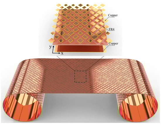
Figure 1.
A schematic representation of the layering of a single periodic cell and the flexibility effect of the proposed design absorber consisting of multiple periodic cell structures.
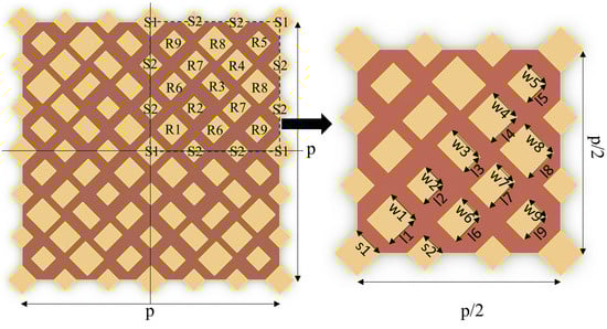
Figure 2.
The constituent subunits of the top pattern layer in a periodic cell and the corresponding dimensions of each subunit.
To determine the optimal dimensions of each structural parameter, we employed the FDTD (Finite-Difference Time-Domain) method. In the simulation, the designed model is placed on the XOY plane, with the incident plane electromagnetic propagating along the Z-axis. Periodic boundary conditions are applied along the X and Y axes, while an open boundary condition is set along the Z-axis. Since the thickness of the metal backing layer is greater than the skin depth of the electromagnetic waves in the operation frequency range, the transmission coefficient is considered to be zero. The optimized structural parameters are shown in Table 1.

Table 1.
The geometric parameters of the copper patches.
Figure 3 shows the reflection and absorption spectra for normal incidence. It can be seen that the reflectance is below −10 dB in the 75–110 GHz frequency range, with the minimum reflectance occurring at 84.5 GHz with a value of −36 dB. The average absorption within the 75–110 GHz range exceeds 94%, effectively covering the entire W-band.
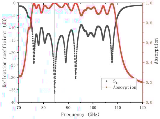
Figure 3.
The reflection coefficient and absorption rate of the MA.
Next, we investigate the impact of the incident angle and polarization state on the absorption performance of the structure. The polarization angle was set to 0°, and the incident angle varied from 0° to 60° with a step size of 15°. As shown in Figure 4a, for TM waves, the variation in the incident angle has a minimal effect on the absorption rate. Even when the incident angle increases to 45°, the average absorption across the entire W-band remains above 90%. However, as shown in Figure 4b, for TE waves, the absorption rate is more sensitive to the change of the incident angle. When the incident angle increases to 15°, the designed metamaterial absorber maintains a nearly constant average absorption rate across the entire W-band. However, as the incident angle increases to 30°, the average absorption decreases significantly to approximately 85%. Further increase in the incident angle leads to weakening of the absorption performance; nevertheless, the designed metamaterial absorber maintains an average absorption of over 79% across the entire W-band.
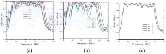
Figure 4.
(a) The influence of the incident angle on the absorption curve for (a) TM and (b) TE polarization. (c) The influence of the polarization angle on the absorption spectrum.
Moreover, the absorption spectra for different polarization angles, shown in Figure 4c, indicate that the proposed structure is insensitive to the changes in polarization angle. This polarization insensitivity arises from the geometrically axisymmetric structure of the pattern design. This feature enhances its potential for practical applications.
Figure 5 displays the instantaneous current density distribution of the MA at an absorption peak frequency of 84.5 GHz. It can be observed that the current on the surface structure flows in a direction opposite and parallel to that on the ground plane. These opposing currents interact to generate a large number of charges, forming two magnetic dipoles. Under the incidence of plane electromagnetic waves, magnetic resonance occurs, effectively enabling the absorption of electromagnetic energy.
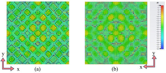
Figure 5.
The surface current distribution, (a) upper surface current distribution, and (b) lower surface current distribution.
To achieve the best performance of the design, the effect of geometric structural parameters on the absorption spectrum was studied. Using the method of controlling variables, each parameter was varied individually in simulations to observe the changes in the absorption spectrum. The simulation results are shown in Figure 6.
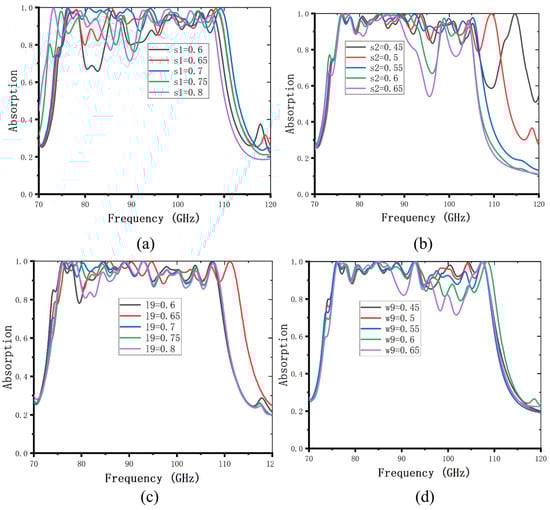
Figure 6.
The influence of different structural dimensions on the absorption characteristics of MA. (a) The influence of the edge length s1 of patch S1, (b) the influence of the edge length s2 of patch S2, (c) the influence of the length l9 of patch R9, and (d) the influence of the width w9 of patch R9.
The absorption for the side length of S1, which varies from 0.6 mm to 0.8 mm, was investigated and the results are shown in Figure 6a. As illustrated in the figure, as the side length of S1 increases, the central frequency of the absorption band shifts toward lower frequencies. Meanwhile, the absorption performance firstly improves and then deteriorates, with the best absorption bandwidth being S1 = 0.7 mm.
Similarly, simulations were conducted by varying the side length of the square patch S2 to from 0.45 mm to 0.65 mm, with the results shown in Figure 6b. The figure clearly indicates that S2 primarily influences the absorption in the high-frequency region. Both excessively large and small side lengths degrade the absorption performance. Comparatively, larger side lengths have a more significant adverse impact on the absorption efficiency.
To investigate the effect of the side length of patch R9 on absorption performance, simulations were conducted with the side length l9 of R9 being changed from 0.6 mm to 0.8 mm, with the results presented in Figure 6c. As shown in Figure 6c, variations in l9 primarily influence the absorption performance around 80 GHz. Finally, Figure 6d shows the absorption by varying the width w9 of R9 from 0.45 mm to 0.65 mm; it is evident that changes in w9 predominantly affect the absorption performance near 100 GHz.
In this structure, the overall absorption performance relies on the combined configuration of all patches. Excessively large or small dimensions of any single patch can degrade absorption efficiency within specific frequency ranges. This highlights the importance of precision in fabrication to ensure optimal absorption performance.
It is well known that perfect absorption can be achieved when the effective impedance of the MA matches the impedance of free space [32]. Figure 7 illustrates the normalized impedance of the MA. Notably, the real part of the impedance is close to one, while the imaginary part approaches zero within the 75–110 GHz range. This indicates that its effective impedance is well-matched to the impedance of free space.
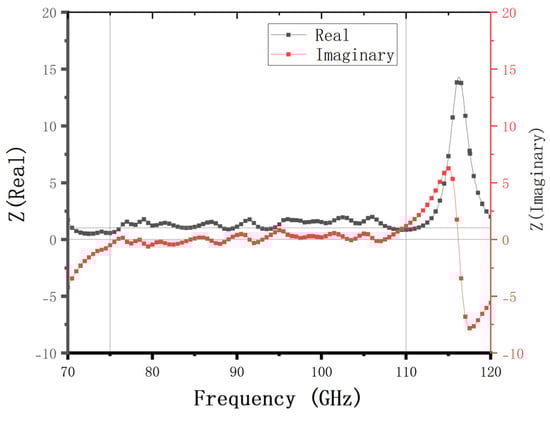
Figure 7.
The real and imaginary parts of the equivalent impedance of the MA in the frequency range of 70 GHz to 120 GHz.
3. Fabrication and Measurement
A sample, where the overall size of the structure is 23 cm × 23 cm, was fabricated using PCB printing technology, as shown in Figure 8a. The sample weight is 31.2 g, which is less than 600 g per square meter. The S11 parameters of the sample were tested using an AV3672D vector network analyzer(CECSYS Technology Corporation, China). Calibration was performed before testing. Due to the target frequency band being in the W-band, an extender module and corresponding horn antennas were utilized during the measurements. The measured absorption curve is shown in Figure 8b, with an average absorption rate of approximately 93.4% over the frequency range of 75–110 GHz, demonstrating excellent performance across the entire W-band. The discrepancies between the measurement and simulation results can be attributed to several factors related to manufacturing tolerances. These include inconsistencies in the thickness of the dielectric layer, variations in the structural dimensions of the unit cells, and processing deviations. Additionally, differences in the dielectric constant of the dielectric layer between the simulation and experiment may also contribute to the deviations.
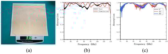
Figure 8.
(a) The prefabricated prototype of the designed MA and its weight; (b) the simulated and measured absorption spectra at normal incidence; (c) the absorption spectra at different polarization angles.
Next, to verify the polarization-insensitive characteristics of the MA, the fabricated sample was tested by rotating it around the propagation axis of the incident wave. As shown in Figure 8c, as the polarization angle increases, the absorption performance of the MA sample is almost constant, with the absorption peak remaining nearly unchanged. This demonstrates that the designed MA exhibits good polarization stability.
To investigate the absorption performance under bending conditions, the MA samples were made to conform to cylinders with diameters of 66 mm, 82 mm, 110 mm, and 130 mm. In each experiment, a piece of copper foil bent to the same radius was used as a reference. The normalized S11 curves for the bent samples compared to the flat state are shown in Figure 9. The results indicate that the reflection increases with decreases in the curvature radius, demonstrating that greater deformation exerts negative impacts on the MA’s performance [33]. Specifically, as the radius of the attached cylinder decreases, both the peak absorption and the bandwidth change. The change in bandwidth is due to the fact that the normal incidence of electromagnetic waves is primarily reflected in the central region of the MA, while other areas may not be fully guaranteed. Meanwhile, the peak absorption frequency changes more obviously at lower frequencies. It can be explained that with the increase in curvature, the effective edge length of the resonant unit decreases, causing the resonant frequency to shift toward higher frequencies. However, the test results show that even when the MA adheres to a cylinder with a diameter of 66 mm, it maintains an average absorption rate of 90% across the W-band. This demonstrates its strong mechanical adaptability and reliable performance under bending conditions.
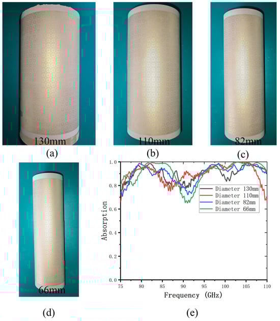
Figure 9.
The responses of MA samples under different bending radii: (a–d) prototypes attached to cylindrical surfaces with diameters of 66 mm, 82 mm, 110 mm, and 130 mm, demonstrating bending adaptability; (e) the normalized absorption rate of the prototype under different bending conditions.
Table 2 compares our proposed structure with some previously reported broadband absorbers, and it can be seen that the proposed absorber is significantly thinner than the previously reported MAs. This ultra-thin characteristic enhances its flexibility and reduces its impact on system integration. In terms of absorption performance, while the proposed design does not achieve the widest absorption band, it effectively covers the entire W-band, which is crucial for practical applications.
Table 2.
A comparison of related MAs.
Regarding fabrication methods, the carbon-based composite absorber in ref. [26] was synthesized through a multi-step process, which is complex and time-consuming. The 3D printing technique used in ref. [27] follows a layer-by-layer material deposition process to construct three-dimensional structures. However, the cost of 3D printing remains higher than conventional manufacturing methods, especially for large-scale production. Additionally, the mechanical strength and durability of 3D-printed metamaterials are still limited. The fabrication method in ref. [28] requires further validation in terms of stability and reliability. In contrast, the PCB fabrication process used in this work involves well-established steps; hence, this mature and scalable technology enables low-cost, high-volume production, making it highly practical for real-world applications.
4. Conclusions
This paper proposes a flexible and broadband absorber intended for W-band absorption, with a classic sandwich structure combined with a tiled arrangement of multiple patches. The MA achieves broadband absorption exceeding 94% within the frequency range of 75–110 GHz, effectively covering the entire W-band. With a total thickness of only 0.22 mm and a weight of 31.2 g, the MA is highly suitable for conformal applications on various surfaces. Furthermore, the MA exhibits polarization insensitivity and good angular stability. Fabricated using PCB printing technology, this design offers advantages such as structural simplicity and a low manufacturing cost compared to other methods for producing broadband millimeter-wave absorbers. In conclusion, the MA presented in this work provides a novel and efficient solution for W-band millimeter-wave absorption.
Author Contributions
Conceptualization and model, J.Z. and L.C.; numerical simulation, G.G. and M.S.; funding acquisition, supervision, project administration, and resources, J.Z. and Y.S.; experiments, writing—original draft preparation, G.G.; writing—review and editing, J.Z., Z.Y. and J.Y. All authors have read and agreed to the published version of the manuscript.
Funding
This work is supported by the Dreams Foundation of Jianghuai Advance Technology Center (no. 2023-ZM01D007).
Data Availability Statement
The data supporting the findings of this study are available within the article.
Conflicts of Interest
The authors declare no conflicts of interest.
References
- Lin, W.; He, Q.; Cheng, T.; Chen, H.; Liu, C.; Liu, J.; Hong, Z.; Hu, X.; Guo, Y. A Method for Retrieving Cloud Microphysical Properties Using Combined Measurement of Millimeter-Wave Radar and Lidar. Remote. Sens. 2024, 16, 586. [Google Scholar] [CrossRef]
- Cuadrado-Calle, D.; Piironen, P.; Ayllon, N. Solid-state diode technology for millimeter and submillimeter-wave remote sensing applications: Current status and future trends. IEEE Microw. Mag. 2022, 23, 44–56. [Google Scholar] [CrossRef]
- Wang, S.; Mei, L.; Liu, R.; Jiang, W.; Yin, Z.; Deng, X.; He, T. Multi-modal fusion sensing: A comprehensive review of millimeter-wave radar and its integration with other modalities. IEEE Commun. Surv. Tutor. 2024, 27, 322–352. [Google Scholar] [CrossRef]
- Ma, Z.; Choi, J.; Yang, L.; Sohn, H. Structural displacement estimation using accelerometer and FMCW millimeter wave radar. Mech. Syst. Signal Process. 2023, 182, 109582. [Google Scholar] [CrossRef]
- Roberts, I.P.; Zhang, Y.; Osman, T.; Alkhateeb, A. Real-world evaluation of full-duplex millimeter wave communication systems. IEEE Trans. Wirel. Commun. 2024, 23, 10803–10819. [Google Scholar] [CrossRef]
- Khan, J.; Ullah, S.; Ali, U.; Tahir, F.A.; Peter, I.; Matekovits, L. Design of a millimeter-wave MIMO antenna array for 5G communication terminals. Sensors 2022, 22, 2768. [Google Scholar] [CrossRef]
- Niu, Y.; Li, Y.; Jin, D.; Su, L.; Vasilakos, A.V. A survey of millimeter wave communications (mmWave) for 5G: Opportunities and challenges. Wirel. Netw. 2015, 21, 2657–2676. [Google Scholar] [CrossRef]
- Lawler, N.B.; Evans, C.W.; Romanenko, S.; Chaudhari, N.; Fear, M.; Wood, F.; Smith, N.M.; Wallace, V.P.; Iyer, K.S. Millimeter waves alter DNA secondary structures and modulate the transcriptome in human fibroblasts. Biomed. Opt. Express 2022, 13, 3131–3144. [Google Scholar] [CrossRef]
- El Khoueiry, C.; Moretti, D.; Renom, R.; Camera, F.; Orlacchio, R.; Garenne, A.; Poulletier De Gannes, F.; Poque-Haro, E.; Lagroye, I.; Veyret, B. Decreased spontaneous electrical activity in neuronal networks exposed to radiofrequency 1,800 MHz signals. J. Neurophysiol. 2018, 120, 2719–2729. [Google Scholar] [CrossRef]
- You, X.; Upadhyay, A.; Cheng, Y.; Bhaskaran, M.; Sriram, S.; Fumeaux, C.; Withayachumnankul, W. Ultra-wideband far-infrared absorber based on anisotropically etched doped silicon. Opt. Lett. 2020, 45, 1196–1199. [Google Scholar] [CrossRef]
- Cai, B.; Yang, L.; Wu, L.; Cheng, Y.; Li, X. Dual-narrowband terahertz metamaterial absorber based on all-metal vertical ring array for enhanced sensing application. Phys. Scr. 2024, 99, 095503. [Google Scholar] [CrossRef]
- Tian, W.; Yang, L.; Cai, B.; Cheng, Y.; Chen, F.; Luo, H.; Li, X. Design and Analysis of Dual-Band Metasurface Filter for Pulse Waves Based on Capacitive Nonlinear Circuits. Electronics 2025, 14, 603. [Google Scholar] [CrossRef]
- Foteinopoulou, S.; Economou, E.N.; Soukoulis, C.J. Refraction in media with a negative refractive index. Phys. Rev. Lett. 2003, 90, 107402. [Google Scholar] [CrossRef] [PubMed]
- Xi, S.; Chen, H.; Jiang, T.; Ran, L.; Huangfu, J.; Wu, B.-I.; Kong, J.A.; Chen, M. Experimental verification of reversed Cherenkov radiation in left-handed metamaterial. Phys. Rev. Lett. 2009, 103, 194801. [Google Scholar] [CrossRef]
- Aieta, F.; Genevet, P.; Kats, M.A.; Yu, N.; Blanchard, R.; Gaburro, Z.; Capasso, F. Aberration-free ultrathin flat lenses and axicons at telecom wavelengths based on plasmonic metasurfaces. Nano Lett. 2012, 12, 4932–4936. [Google Scholar] [CrossRef]
- Chen, J.; Wang, Y.; Jia, B.; Geng, T.; Li, X.; Feng, L.; Qian, W.; Liang, B.; Zhang, X.; Gu, M. Observation of the inverse Doppler effect in negative-index materials at optical frequencies. Nat. Photonics 2011, 5, 239–242. [Google Scholar] [CrossRef]
- Chen, X.; Li, C.-F. Lateral shift of the transmitted light beam through a left-handed slab. Phys. Rev. E 2004, 69, 066617. [Google Scholar] [CrossRef]
- Li, K.; Lu, H.; Bi, M.; Qi, L.; Weng, X. A flexible metamaterial absorber with temperature-insensitive design at microwave frequencies. Smart Mater. Struct. 2023, 32, 105027. [Google Scholar] [CrossRef]
- Zhou, Q.; Xue, B.; Gu, S.; Ye, F.; Fan, X.; Duan, W. Ultra broadband electromagnetic wave absorbing and scattering properties of flexible sandwich cylindrical water-based metamaterials. Results Phys. 2022, 38, 105587. [Google Scholar] [CrossRef]
- Xie, Y.; Liu, Z.; Zhou, F.; Luo, X.; Cheng, Z.; Yang, R.; Cheng, J.; Yang, G. A multifrequency narrow-band perfect absorber based on graphene metamaterial. Diam. Relat. Mater. 2023, 137, 110100. [Google Scholar] [CrossRef]
- Wei, X.; Wang, J.; Zhou, F.; Tan, R.; Liu, J.; Chen, P. A broadband low-profile microwave absorber based on ferromagnetic material doped hybrid stereo metamaterial. J. Phys. D Appl. Phys. 2023, 57, 015101. [Google Scholar] [CrossRef]
- Han, K.; Shim, H.B.; Hahn, J.W. Optically Transparent Single-Layer Frequency-Selective Surface Absorber for Dual-Band Millimeter-Wave Absorption and Low-Infrared Emissivity. Adv. Photonics Res. 2023, 4, 2200009. [Google Scholar] [CrossRef]
- Song, N.; Sun, Q.; Xu, S.; Shan, D.; Tang, Y.; Tian, X.; Xu, N.; Gao, J. Ultrawide-band optically transparent antidiffraction metamaterial absorber with a Thiessen-polygon metal-mesh shielding layer. Photonics Res. 2023, 11, 1354–1363. [Google Scholar] [CrossRef]
- Gan, R.; Yu, M.; Li, S.; Li, Y.; Fang, B.; Qi, S. A magnetic control reconfigurable coded electromagnetic absorbing metamaterial. Compos. Sci. Technol. 2022, 217, 109098. [Google Scholar] [CrossRef]
- Liu, S.; Pei, C.; Khan, L.; Wang, H.; Tao, S. Multiobjective optimization of coding metamaterial for low-profile and broadband microwave absorber. IEEE Antennas Wirel. Propag. Lett. 2023, 23, 379–383. [Google Scholar] [CrossRef]
- Suda, Y.; Matsuo, R.; Yoshii, T.; Yasudomi, S.; Tanimoto, T.; Harigai, T.; Takikawa, H.; Setaka, T.; Matsuda, K.-I.; Suizu, K. Electromagnetic wave absorption properties of carbon nanocoil composites in the millimeter waveband. In AIP Conference Proceedings; AIP Publishing: New York, NY, USA, 2018. [Google Scholar]
- Petroff, M.; Appel, J.; Rostem, K.; Bennett, C.L.; Eimer, J.; Marriage, T.; Ramirez, J.; Wollack, E.J. A 3D-printed broadband millimeter wave absorber. Rev. Sci. Instrum. 2019, 90, 024701. [Google Scholar] [CrossRef]
- Kamei, T.; Shima, H.; Yamamoto, T.; Ogino, S.; Ishii, S. Millimeter-wave absorption properties of thin wave absorber in free space with new porous carbon material. Wirel. Eng. Technol. 2017, 8, 51–58. [Google Scholar] [CrossRef]
- Huang, H.; Xia, H.; Guo, Z.; Huang, S.; Li, H.; Wu, Y. polarization-independent and broadband microwave metamaterial absorber based on three-dimensional structure. J. Mod. Opt. 2018, 65, 1521–1528. [Google Scholar] [CrossRef]
- Deng, G.; Xia, T.; Yang, J.; Yin, Z. Triple-band polarisation-independent metamaterial absorber at mm wave frequency band. IET Microw. Antennas Propag. 2018, 12, 1120–1125. [Google Scholar] [CrossRef]
- Singh, P.K.; Korolev, K.A.; Afsar, M.N.; Sonkusale, S. Single and dual band 77/95/110 GHz metamaterial absorbers on flexible polyimide substrate. Appl. Phys. Lett. 2011, 99, 264101. [Google Scholar] [CrossRef]
- Huang, X.; Cao, M.; Wang, D.; Li, X.; Fan, J.; Li, X. Broadband polarization-insensitive and oblique-incidence terahertz metamaterial absorber with multi-layered graphene. Opt. Mater. Express 2022, 12, 811–822. [Google Scholar] [CrossRef]
- Sood, D.; Tripathi, C.C. Broadband ultrathin low-profile metamaterial microwave absorber. Appl. Phys. A 2016, 122, 332. [Google Scholar] [CrossRef]
Disclaimer/Publisher’s Note: The statements, opinions and data contained in all publications are solely those of the individual author(s) and contributor(s) and not of MDPI and/or the editor(s). MDPI and/or the editor(s) disclaim responsibility for any injury to people or property resulting from any ideas, methods, instructions or products referred to in the content. |
© 2025 by the authors. Licensee MDPI, Basel, Switzerland. This article is an open access article distributed under the terms and conditions of the Creative Commons Attribution (CC BY) license (https://creativecommons.org/licenses/by/4.0/).