Review

Application of Organic Light-Emitting Diodes and Photodiodes in Optical Control and Detection of Neuronal Activity

by
Marcin Kielar
1,2,*,
Matthew Kenna
2,
Philippe Blanchard
1 and
Pankaj Sah
2,*
1
MOLTECH-Anjou Laboratory, The University of Angers, CNRS, SFR MATRIX, F-49000 Angers, France
2
Queensland Brain Institute, The University of Queensland, St Lucia, QLD 4072, Australia
*
Authors to whom correspondence should be addressed.
Photonics 2025, 12(3), 281; https://doi.org/10.3390/photonics12030281
Submission received: 31 January 2025 / Revised: 15 March 2025 / Accepted: 15 March 2025 / Published: 18 March 2025
(This article belongs to the Special Issue Optical Imaging Innovations and Applications)

Abstract

:
Optical techniques to study neuronal activity have greatly advanced the field of neuroscience over recent decades. Multichannel silicon-based recording probes combined with optical fibers allow for simultaneous recording and manipulation of neuronal activity that underpins cognitive processes and behavior. The recent development of neural probes incorporating organic light-emitting diodes (OLEDs) and photodiode-based organic photodetectors (OPDs) offer additional advantages of biocompatibility, ultra-small footprint, multifunctionality, and low cost. These developments are ushering in a new generation of devices that are ideal for the interrogation of neuronal activity in vitro and in vivo. In this review, we discuss recent progress in OLED- and OPD-based neural probes, their applications in the optical control of neuronal function, and current challenges and prospects for the future.

1. Introduction

Mapping large-scale neural activity in the brain is crucial to understanding neuronal circuits that are involved in cognitive processes and behavioral outcomes, as well as to track neurological impairments such as Alzheimer’s or Parkinson’s diseases (PD) [1,2,3,4,5,6]. This knowledge is needed to develop new treatments for brain diseases and disorders. In the long term, these developments will lead to improvements in the overall quality of life of patients suffering from these illnesses. To progress our understanding of brain function, numerous neuroengineering techniques have been developed over past decades, ranging from electrical recordings to optical manipulation of neuronal activity that can be applied across many brain regions [7,8]. Multichannel silicon-based probes incorporating metals such as titanium and gold, as well as metal alloys (e.g., platinum–iridium), optical fibers, monochromatic light sources, and photodetection camera systems (CMOS- and CCD-based), and entire microscope setups have been developed to specifically image and optically control the activity of defined neural populations [9,10,11].
However, despite providing invaluable data and insights into the neural activity that underpins behavior and cognition, these techniques come with several restrictions, such as biocompatibility, invasiveness, and high cost. To tackle these limitations, neural probes based on organic optoelectronic devices have emerged as complementary tools to map neuronal activity with high temporal and spatial resolution [12,13,14,15]. This review summarizes recent progress in the development of optical neural probes, often referred to as optoprobes, based on organic semiconductors: organic light-emitting diodes (OLEDs) and photodiode-based organic photodetectors (OPDs). The advantages of using organic electronics to study neuronal activity are discussed with an emphasis on device design, working principles, and key differences from current technologies. In addition, the practical applications of OLED and OPD technology applied in vitro and in vivo are discussed in chronological order. Finally, current challenges, such as flexibility and miniaturization, are examined in detail. Overall, this review aims to provide an understanding of the current capabilities of organic optoprobes, as well as the hurdles to their development, and prospects for the future.

2. Tracking Neuronal Activity

2.1. Communication: Action Potentials and Synapses

A nerve cell or neuron is the basic unit of the nervous system composed of a cell body (soma), branching extensions (dendrites), and a single long extension (axon) that branches into terminals (Figure 1a). A single neuron expresses a variety of ion channels across its cell membrane that allow positive or negative ions to flow into or out of the cell [16]. The relative ratio of these ions, extracellular to intracellular, and the permeability of each ion channel determines the membrane potential or voltage across the cell membrane [17]. The opening of cationic ion channels can initiate a rapid sequence of changes in this voltage and, once past a defined threshold, will trigger a nerve impulse (electrical signal) called an action potential (AP). This signal travels from the cell body down the length of the axon to the axon terminal. At the junction between two neurons (synapse), when an AP reaches the presynaptic terminal, a neurotransmitter (chemical molecule) is released into the space between the (presynaptic) axon terminal and the (postsynaptic) dendrite of a nearby neuron [18,19]. Neurotransmitters bind to specialized receptors on the postsynaptic cell, causing various ion channels that span the membrane to be opened. This allows positive or negative ions to travel through the channel, leading to changes in the membrane potential. A given neuron receives hundreds or thousands of excitatory or inhibitory inputs from neighboring cells, resulting in dynamic changes in membrane potential. When the membrane voltage reaches the threshold potential, an AP is triggered, propagating the signal along a neural network. Neuronal communication via bioelectrical signals is intricately regulated as a balance between these excitatory and inhibitory influences [20].

2.2. Mapping the Brain’s Electrical Activity

A key finding in neuroscience was the recognition that the activity of highly structured neural networks consisting of large numbers of interconnected neurons is responsible for complex processes that are fundamental for behavior and survival. However, how these neural circuits process and represent information to elicit specific brain functions (such as the control of movement or the storage of information as memories) is just starting to be understood [21]. A central tenet of the neuroscientific approach to deciphering the code used by the brain is to record and/or manipulate neuronal activity during defined tasks. Single neuron electrical activity can be recorded by inserting a small electrode into a neuron, allowing direct measurement of intracellular neuronal activity (Figure 1a). Voltage-, current-, and patch-clamp techniques have been developed to track the activity of single neurons [22]. If the electrode is located externally from the neuron, in continuity with the extracellular space, single-unit or multi-unit extracellular activity can be tracked, depending on the electrode size and geometry of the system. For large electrodes, only the net activity of many cells is recorded, often referred to as local field potential (LFP). One can note here that with the support of many electrodes, individual cells can still be identified using a process called spike sorting (Figure 1b) [23]. Historically, these extracellular recording techniques were developed to record individual or, at most, several neurons. These probes have now advanced to house many electrical contacts, allowing simultaneous recordings from hundreds of neurons (e.g., silicon neural probes) [10,24]. Stimulating neural probes have also been engineered, with the most notable example being platinum/iridium-based electrodes that can also be implanted into humans to provide therapeutic benefits in a procedure called Deep Brain Stimulation (DBS) [25]. DBS was initially implemented for the treatment of PD and is now routinely used to treat a range of movement disorders, such as essential tremor, dystonia, and others [26]. More recently, DBS electrodes are also being used to treat some psychiatric disorders [27,28,29].

2.3. Optical Interrogations of Neural Circuits

While electrodes provide high temporal resolution and directly measure electrical activity, they are limited in their ability to selectively record or manipulate neuronal activity within specific neural populations. However, the advent of genetic tools for identifying neuronal subtypes and pathways has enabled the introduction of genetically encoded calcium indicators (GECIs), such as GCaMP6, into genetically-defined neurons [30]. GECIs are fluorescent proteins that undergo a change in their fluorescence intensity in response to fluctuations in cytosolic calcium levels, providing a reliable proxy for neuronal activity, as action potentials (APs) are closely associated with an influx of calcium ions into the cell. To visualize these fluorescence changes, GECIs must be excited with light of a specific wavelength, traditionally using a fluorescence microscope or high-powered laser. By coupling this with high-speed cameras, researchers can track activity in specific neurons both in vitro and in vivo (Figure 1c).
In parallel, light-responsive proteins, known as opsins, have been developed to use light to control the electrical activity of neuronal populations. These so-called “optogenetic” proteins are genetically inserted into the neuronal membrane and respond to specific wavelengths of light by allowing the flow of charged ions into or out of the cell, thus controlling neuronal activity (Figure 1c). For example, Channelrhodopsin-2 (ChR2) is an ion channel that opens in response to blue light, leading to depolarization and the initiation of action potentials in the targeted neurons. With these tools, it is possible to monitor and manipulate the neuronal activity of defined subsets of neurons to understand their function [31].
Although the development of calcium imaging and optogenetics has revolutionized the study of the brain, their practical implementation requires a suite of advanced optical equipment. For example, using optogenetic approaches to manipulate neuronal activity requires the insertion of high-grade optical fibers that deliver light to the targeted cell population. Similarly, recording neuronal activity through fluorescent markers involves the relay of spectrally separated fluorescence emissions to external detectors for filtering and digitalization. Notably, the insertion of large fiber optic implants and camera systems results in damage to the overlying brain tissue, which is often aggravated by low levels of biocompatibility. Similarly, when recordings are made in awake behaving animals, the presence of the tether, together with the optical cable, can induce motion artefacts in the camera images that limit signal fidelity [32]. This can also produce micro-motions that are detrimental to the neuronal interface due to glial scarring [33]. Lastly, the cameras generally used to record the activity of GECI-expressing cells operate at normal video rates (33 to 50 Hz) and are unable to record with the higher temporal fidelity required for more advanced imaging. For example, recording neuronal activity through the burgeoning approach of using genetically encoded voltage indicators (GEVIs) requires the ability to detect small fluorescence changes over very short timescales (in the kHz range) [34]. Thus, advanced camera systems are necessary to benefit from the resolution that GEVIs provide, which has slowed the uptake of this approach in neuroscience. Finally, the sheer size of these implantable devices means that typically only a single device can be inserted in one or a few brain regions. As such, these imaging techniques are limited in their capacity to provide information at the level of the whole brain.

2.4. Complementary Role of Magnetic Resonance Imaging

To record neuronal activity from the whole brain, functional magnetic resonance imaging (fMRI) has been developed as a complementary tool to electrical and optical interrogations of neural circuits. It enables monitoring of neuronal activity from subjects over long temporal spans, providing a general guide to the brain regions active during behavioral tasks [35]. Notably, fMRI does not provide information about specific neural activity, and combining fMRI with direct neural recordings would be desirable. However, the aforementioned silicon neural probes and camera-based imaging techniques are not compatible with fMRI [36]; the commercially available probes lead to imaging artefacts due to distortion of the magnetic field [37,38], which is caused by high concentrations of paramagnetic metals. This is unfortunate, as the fusion of calcium imaging, optogenetics, and fMRI would provide deep insights given the complementary spatiotemporal properties of these techniques. To synchronize the fMRI imaging with optoelectrical signals in the brain, fMRI-compatible electrodes that align with the susceptibility of their environment would be highly desirable.

2.5. Advantages of Organic Neural Probes

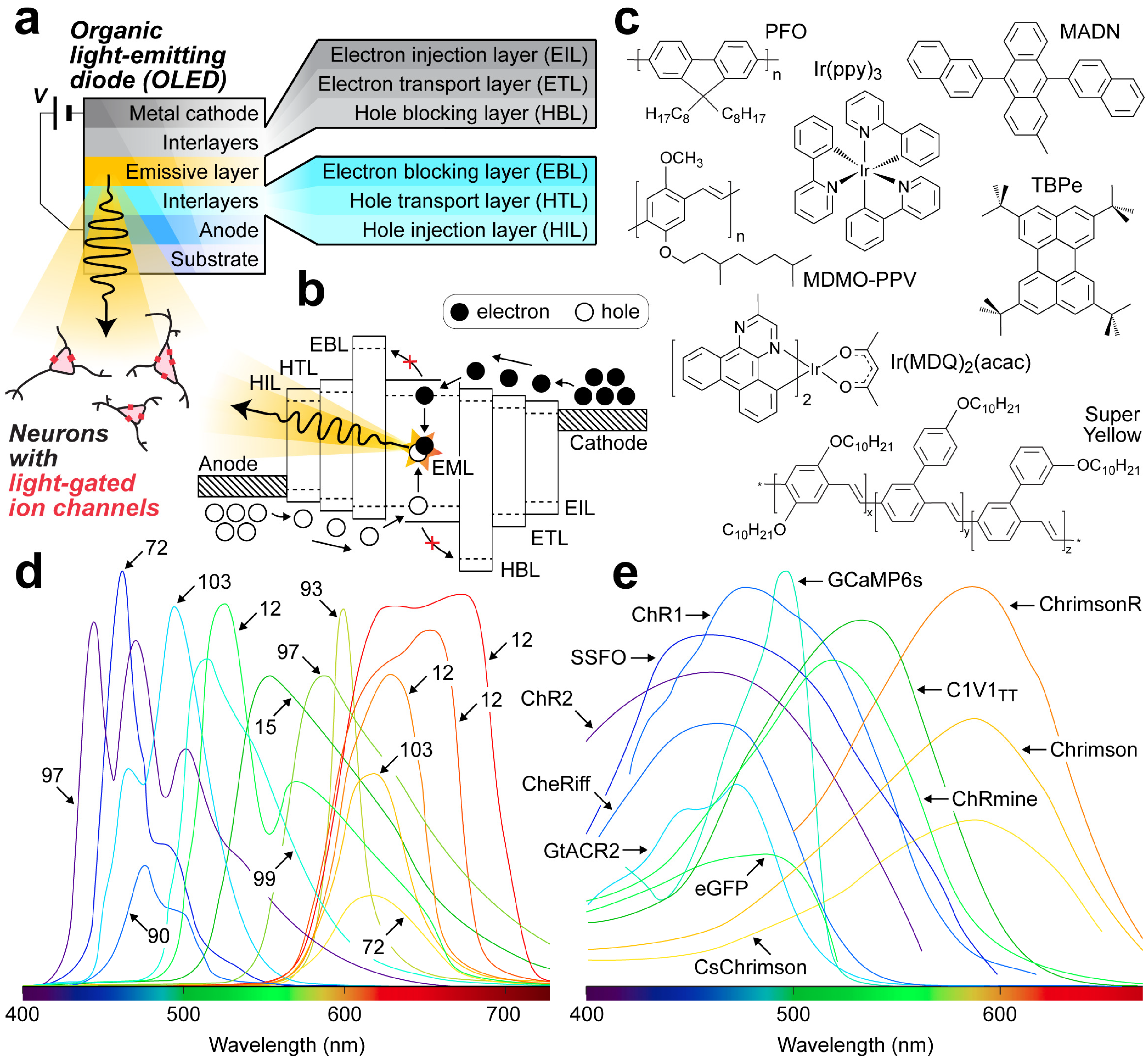
2.5.1. Optoelectronic Performance

To address the above limitations, a new type of neuroengineering optoelectronic device based on soft and flexible organic components has begun to be optimized for neuroscience applications. After the discovery of conductive plastics resulting from the doping (oxidation) of π-conjugated polymers [39], the subsequent development of organic semiconductors associated with π-conjugated systems in their neutral states has led to rapid growth in the field of organic electronics. This has led to the development of next-generation organic solar panels (organic photovoltaic cells, OPVs) [40] and reliable organic light-emitting diodes (OLEDs) [41]. OLED technology has progressed into the commercial landscape and is widely used in smartphones, television displays, and light sources for general lighting and automotive applications. Organic photodiodes (OPDs) [42] and transistors (OFETs) [43] have also shown potential in biosensing applications by converting a biological response into an electrical signal (e.g., pulse oximeter) [44,45]. Importantly, these devices not only demonstrate detection speeds up to the kHz and MHz ranges [46] but also feature a detectivity level that rivals low-noise silicon photodiodes [47,48]. The electronic noise of the photodetector signal sets the device sensitivity and defines the limit of what can be detected, that is, the minimum incident light power at which the signal-to-noise ratio (SNR) is unity [49]. This threshold is called the noise equivalent power (NEP), and a smaller NEP corresponds to a more sensitive detector. Many mechanisms have been reported as sources of electronic noise inside organic photodiodes, and more importantly, these sources are frequency-dependent [49,50]. The reciprocal of the NEP normalized per square root of the sensor’s area and frequency bandwidth reflects the device-specific detectivity (D*) and allows direct comparison of different devices in terms of sensitivity [51]. A higher D* corresponds to a more sensitive detector. Whether it is for chemical, biological, or photosensing applications, low-noise next-generation optoelectronic sensors largely benefit from functionally engineered conjugated organic semiconductors [52,53,54].

2.5.2. Biocompatibility, Flexibility, and MRI-Compatibility

Importantly, these carbon-based materials have the additional advantage of biocompatibility when compared to inorganic devices. It has been observed that metal electrodes implanted in the brain trigger an inflammatory and wound-healing response in surrounding neurons and glial cells, including astrocytes and microglia [55]. Therefore, probes based on organic materials are ideal candidates to mitigate the inflammatory response and improve recording performance in vivo [56,57]. Organic semiconductor materials are easily color-tunable (i.e., they can be tuned to sense and emit different wavelengths of light) [58,59,60,61], resulting in a versatile suite of organic materials that can align with the array of proteins used in neuroscience investigations [62]. Furthermore, the complete probe can be deposited on flexible substrates with a minimal thickness of 1.5 μm [63] or even become substrateless [64]. The use of ultra-thin plastic substrates allows the probe to be flexible and/or stretchable, substantially minimizing the invasiveness of the approach. Indeed, it has been found that rigid electrodes based on metal or glass are subject to micromotions that can be detrimental to the neuronal interface due to glial scarring [33,65]. Although metal electrodes are still present in many organic optoelectronic devices (e.g., the cathode is made of silver, gold, or aluminum), they are classed as non-magnetic materials, and their thickness is usually below 200 nm. OLEDs featuring these ultrathin and nonmagnetic metals generate no artefact under MRI and a minimal signal loss [66], which gives them significant advantages for applications in neuroimaging. In addition, the presence of thin metal layers in OLEDs and OPDs does not hinder their biocompatibility, as these light-emitting and -absorbing devices can be entirely encapsulated using polymeric dielectric materials such as parylene [66].

2.5.3. Multifunctionality

Organic semiconductors are able to incorporate two or more distinct optoelectronic functions in the same device, which is a significant improvement over conventional optogenetic systems. To simultaneously record and manipulate neuronal activity, multiple light sources and camera systems are typically needed, each emitting or being sensitive to a particular wavelength of light [67]. In case of spectral overlap and crosstalk, additional cut-off filters, amplification lenses, or noise-reduction systems are used, which contributes to the complexity of the experimental equipment. As such, the most appealing advantage of OLEDs and organic photodiodes in the context of optogenetic approaches is their ability to provide fine spatial optical control of neurons in a lens-free configuration [15,68]. Organic electronics not only provide stable, ultra-narrowband, low-power light sources [69,70] but can also offer dual-color emission or detection within a single device or with two OLEDs stacked [71,72,73,74]. Finally, single devices featuring both OLED and OPD functions, as well as OPV (organic solar cell) functions, have been suggested [75,76,77]. Such all-in-one systems offer the potential of optically manipulating and recording neuronal activity while maintaining the ease of fabrication and ultra-small footprint. State-of-the-art OPVs demonstrate power conversion efficiencies exceeding 20% [78]. The addition of the OPV function could lead to wireless, solar-powered optoelectronic systems for in vivo studies [79].
Multifunctional organic neural probes incorporating OLEDs and OPDs could also host ultrathin metal or polymeric electrodes (bioelectrodes), enabling both optical and electrical interrogations of the brain (Figure 2). Organic conducting polymers such as poly(3,4-ethylenedioxythiophene) (PEDOT:PSS) could be used as an additional coating, which has been shown to greatly reduce electrode impedance and enhance inflammatory stability [80,81]. Metal-free polymeric bioelectrodes based on PEDOT:PSS for neural recordings in vivo have also demonstrated an adequate signal-to-noise ratio and good stability [81,82]. Taken together, due to the unique properties of organic materials and fabrication methods, multifunctional neural probes offering bioelectrical stimulation and recording, as well as photoexcitation and photodetection, are on the verge of being applied to the study of the brain.

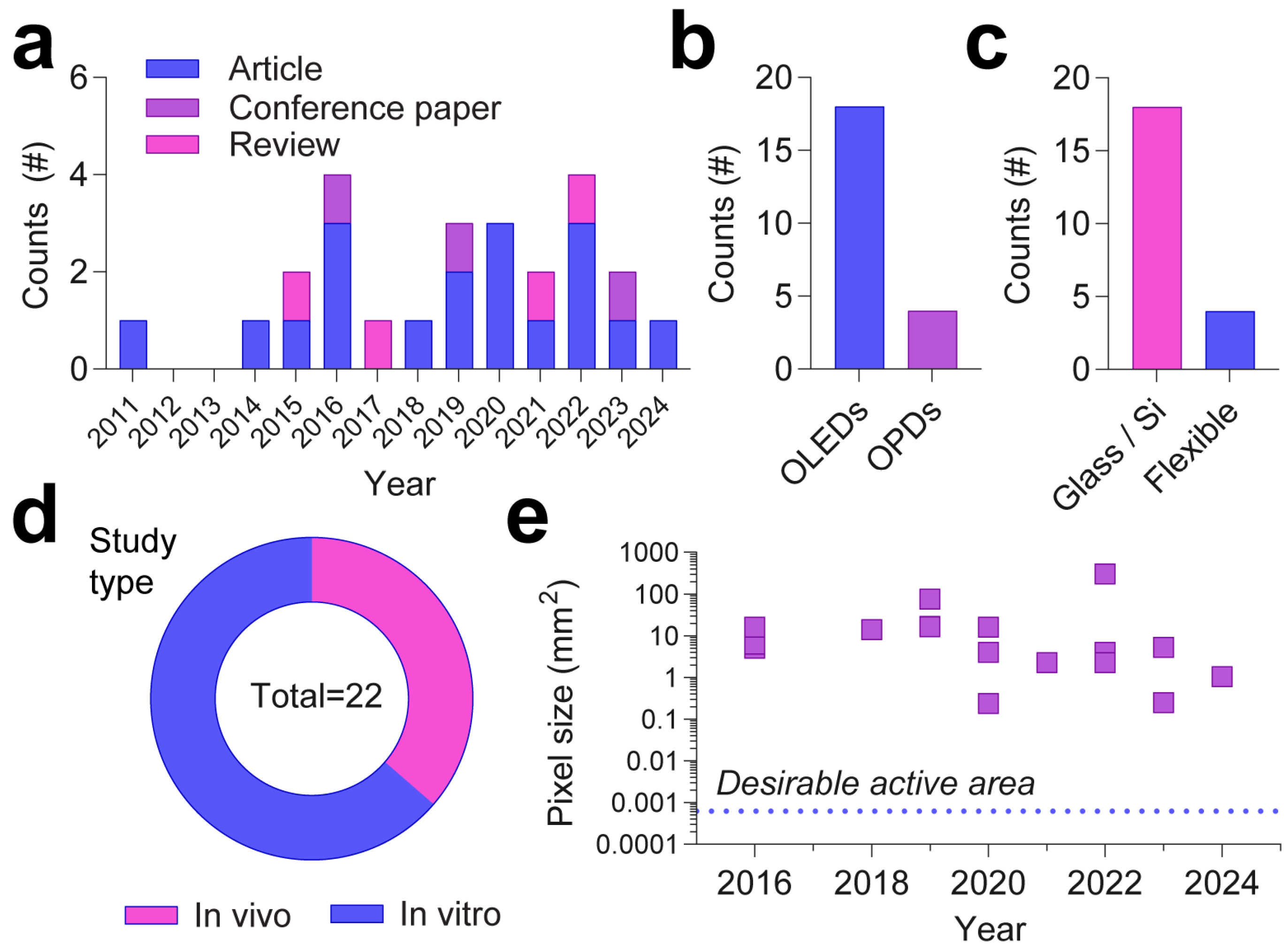
2.6. Applications of OLEDs and OPDs in Mapping Neuronal Activity

2.6.1. Organic Light-Emitting Diodes

OLEDs are ultra-thin light-emitting devices in which an emissive organic layer (EML) is embedded between interlayers and two electrodes (Figure 3a) [83]. Devices are driven using direct current (DC), and when power is supplied, positive charges (holes) injected from the anode migrate to the cathode, while electrons injected from the cathode migrate to the anode [84]. Low and high work function (WF) electrodes are needed for the effective injection of electrons and holes, respectively. Before reaching the emissive material, positive and negative charges travel through a series of thin organic interlayers that assist their movement and improve the OLED efficiency by preventing non-radiative losses and short circuits [83,84,85]. Depending on the device architecture, one can utilize hole and electron injection layers (HILs and EILs, respectively), hole and electron transport layers (HTLs and ETLs, respectively), and electron and hole blocking layers (EBLs and HBLs, respectively) for this purpose. The highest occupied molecular orbital (HOMO) and lowest unoccupied molecular orbital (LUMO) energy levels of these interlayers are crucial for enhancing charge transport from electrodes to the EML [86,87]. Typically, a cascade energy level alignment of these interlayers for holes (HOMO levels) and electrons (LUMO levels) is preferred (Figure 3b). Hole and electron pairs (excitons) formed in the EML can recombine from a high-energy state to a ground state, resulting in the emission of light. One of the two electrodes and the associated interlayers must remain highly transparent or ultra-thin for the light to escape the device and reach neurons expressing light-gated proteins. Interlayers are generally thinner than 50 nm, and the overall OLED structure is usually less than 500 nm thick, with the substrate—often transparent—typically being the thickest part.
OLEDs offer high tunability, and the selection of an organic material for the EML (Figure 3c) as well as the overall device architecture will determine the device’s emission spectrum (Figure 3d) [88,89]. Early efforts in stimulating neuronal activity focused on designing blue OLED systems capable of exciting the first family of light-gated ion channels, Channelrhodopsin-1 (ChR1) and Channelrhodopsin-2 (ChR2), with their excitation spectra peaking at 490 and 460 nm, respectively (Figure 3e). To target single cells of Chlamydomonas reinhardtii, cultured HEK-293 cells, or cortical neurons in vitro, organic OLEDs relied on an inorganic support, either a silicon-based complementary metal-oxide semiconductor (CMOS) backplane [68,90] or a thin film transistor (TFT) backplane [91,92]. These are necessary to drive the microarrays of OLEDs efficiently without resorting to supplying hundreds of pixels individually, which would be inconceivable given geometric and electronic constraints. OLED devices have also been developed on silicon (Si) substrates, acting as surrogates for future implementation on silicon CMOS chips to allow optogenetic control of retinal cells [93]. Without being “completely organic”, most of these OLED-based hybrid systems have proven efficient in controlling the activity of single live cells and in optogenetic manipulation of individual neurons.
OLED systems with completely organic materials began to emerge from 2016 in a series of in vitro and fluorescence imaging studies that demonstrated their ability to excite common opsins used in neuroscience. Aside from being able to stimulate ChR1 and ChR2, blue OLEDs based on TBPe:MADN emissive systems (Figure 3c) were optimized to activate high-current channelrhodopsin CheRiff (excitation peak 465 nm) in primary cultured neurons [14]. Importantly, the authors also showed that OLED devices were stable across large numbers of stimulation pulses, indicating that such devices offer the durability required for neuronal investigations. A similar OLED architecture has been used to visualize the expression of enhanced green fluorescent protein eGFP (excitation peak 490 nm) in a live culture of fibroblasts [94]. The same OLED device was used as a light source for fluorescence microscopy and calcium imaging, targeting GCaMP6s, a highly sensitive GECI with an excitation peak nearing 500 nm (Figure 3e). Further into the 500 nm range, cultured cortical neurons expressing a green-light sensitive chimeric channel-rhodopsin (C1V1tt) (excitation peak 530 nm) were successfully stimulated in vitro using a green source OLED [95].
While blue and green OLEDs offer significant versatility in neuroscience studies, red-shifted opsins are increasingly used since red light maximizes the penetration depth of the excitation light source into the tissue. To this effect, OLEDs based on the PDY-132 (Super Yellow) emissive compound (Figure 3c) have been shown to be capable of stimulating cultured hippocampal neurons expressing the red-shifted opsin, Chrimson (excitation peak 590 nm) [15,96]. Critically, the Super Yellow OLED device did not require a conventional optical system to activate neuronal activity and was able to triangulate the location of a single neuron when using a multi-OLED approach [15]. In recent years, neuroscience studies have adopted an approach of using multiple opsins in the same neuron, which allows bidirectional modulation of neuronal activity (i.e., activation and/or inhibition) upon photostimulation. Blue and orange OLEDs based on PFO and MDMO-PPV (Figure 3c) have been used for photoactivation of the opsin SSFO (excitation peak at 460 nm) and ChrimsonR (590 nm) in the same neuronal preparation [97]. Similarly, dual-color OLEDs capable of switching between blue and red, or blue and green light were reported to elicit both optogenetic inhibition and excitation in cell cultures [12]. To achieve this, the device featured stacked OLEDs based on MADN:TBPe (blue), Ir(MDQ)2(acac) (red) and Ir(ppy)2(acac) (green) emissive materials (Table 1). Such dual blue-red OLEDs have been used to selectively stimulate GtACR2 (excitation peak 470 nm) and Chrimson, while dual blue-green devices could reliably stimulate cells expressing GtACR2 and ChRmine (520 nm) opsins [12] (Figure 3e). Overall, these proof-of-principle studies in simple neuronal systems have demonstrated that OLED devices are adaptable to a wide range of light-based tools used to investigate neuronal function.
Although OLED devices have proven to be powerful tools for in vitro studies, their significant contribution to neuroscience is through applications to in vivo investigations. Early work harnessing OLED technology in vivo has involved using either fruit flies Drosophila melanogaster [12,72,99,100,102] or transgenic rodents [66,95,103] as model systems. In Drosophila larvae, OLED devices have been used to excite ChR2-expressing motor neurons responsible for locomotion, altering head and tail trajectory [99], as well as contraction of the larvae [100]. With the miniaturization of OLED technology, small linear arrays of OLEDs have been developed, where light can be delivered in a more spatially controlled manner [102]. Such devices have been employed to target specific regions of Drosophila, providing insight into the functioning of the Drosophila neural system [102]. Similar to the aforementioned approach in vitro, dual blue-red OLED systems have been used to target activation and inhibition of motor neurons in Drosophila larvae expressing Chrimson and GtACR2 opsins [12]. Recently, by combining linear arrays of miniaturized OLEDs with dual-color capability, researchers have developed a powerful tool to provide segment-specific modulation of neuronal activity [72]. These devices enable simultaneous multi-site activation and inhibition, as well as the ability to switch between colors without the need for complex optical elements. It is worth noting that these miniaturized dual-color OLED systems could, in principle, be applied to other small model organisms or brain slices.
In other model systems, OLEDs have been reported to evoke an optical stimulation-locked response in a ChR2-expressing transgenic mouse model [95]. In a proof-of-concept experiment, at least three single neuronal units recorded in awake animals were found to respond to blue OLED stimulation. Recently, an implantable deep-brain light delivery system based on OLED technology has been proposed to selectively target brain regions as deep as 5 mm [103]. The neural probe relied on a CMOS backplane to access 1024 individually addressable OLEDs with a 24.5 μm pitch. Orange and blue neural probes based on Ir(MDQ)2(acac) and MADN:TBPe (Figure 3c) were fabricated to selectively activate individual ChRmine- and ChR2-expressing neurons with millisecond-level precision in mice. Although showing superior performance, OLED integration on CMOS significantly increases the complexity of fabrication, as well as the probe thickness and invasiveness. In addition, these devices are unable to benefit from the main advantages of OLEDs, such as flexibility and fMRI-compatibility. To tackle this, an alternative approach has been demonstrated with ultrathin (2 μm), ultraflexible OLEDs, which have been shown to activate ChR2-expressing neurons in rats [66]. Furthermore, optical stimulation from this thin blue OLED configuration to nerve fibers induced contractions of the downstream innervated muscles. A minimal footprint device design reduces the mechanical damage from implantation compared to inorganic counterparts [33]. Importantly, as this optoprobe was MRI compatible, neuronal activity induced by direct OLED stimulation of the brain could also be visualized using MRI. Taken together, these first in vivo studies have shown that organic-based light sources offer considerable advantages in a range of experimental designs and animal models.

2.6.2. Organic Photodiodes

As OLEDs aim to replace conventional light sources, fiber optics, and lenses, photodiode-based OPDs have the potential to replace CMOS and CCD camera systems in fluorescence imaging studies. Their typical device structure consists of an organic active layer nestled between two interlayers and two electrodes [50] (Figure 4a). The active layer consists of electron donor (ED) absorbing photons and generating excitons (electron-hole pairs) and an electron acceptor (EA) assisting in photo-induced electron transfer and exciton dissociation. Although not shown in Figure 4a, we note that the EA also features an absorption spectrum that also contributes to photon absorption, resulting in exciton generation [104]. Interlayers, typically hole and electron blocking layers—HBLs and EBLs, respectively—improve the OPD efficiency by reducing parasitic noise referred to as dark current [105]. WFs of electrodes, as well as HOMO and LUMO levels of organic materials, are carefully selected for efficient photocurrent generation [48] (Figure 4b). As with OLEDs, one of the electrodes must remain transparent to let light in for successful photodetection. The OPD thickness is typically below 400 nm, with the total thickness limited by the choice of substrate.
An early example of an OPD for neuronal photodetection consisted of a hybrid bioorganic interface based on P3HT and PCBM (Figure 4c) [98], which was able to record activity from a network of cultured primary neurons. This was an important stepping stone for further work moving toward the development of an artificial retina based on organic materials [107]. Similarly, OPDs with the same active layer were used to demonstrate the detection of a wide range of natural physiological activities and pathophysiological events, such as epileptiform activity in mouse brain slices (ex vivo). The OPD featured a wide responsivity spectrum (Figure 4d) to measure transmittance changes through brain slices using a halogen (white) light source [101]. These changes are caused by cellular volume variations due to ion fluxes in and out of the neuronal network’s cells.
The use of calcium imaging techniques to record neuronal activity can also be augmented by supplanting traditional camera systems with OPDs. In a set of in vitro experiments on cultured cortical neurons loaded with the fluorescent calcium indicator Cal-520 (Figure 4e), organic photodiodes based on rubrene and C60 (Figure 4c) could reliably detect electrically evoked fluorescent activity with high fidelity and signal-to-noise ratio [13]. With the detection threshold measured at 500 pW cm−2, the fabricated photodiodes could directly detect changes in fluorescent neuronal activity as low as 2.3 nW cm−2. This OPD configuration was also able to record time-locked spontaneous fluorescent transients, demonstrating adequate sensitivity for the detection of physiological events.
Although calcium imaging is currently the most prominent method for the optical mapping of brain activity, the Ca2+ photoresponse is only an indirect measure of neuronal electrical activity since the measurements are performed at low temporal resolution [108]. GECI fluorescence signals typically feature slow decay times (in the order of seconds), while action potentials (APs) operate at millisecond time scales, which cannot be resolved using this technique. To address this limitation, a novel technique of voltage sensing using genetically encoded voltage indicators (GEVIs) has recently been developed [34]. These indicators directly measure the change in voltage inside a neuron, which has been shown to possess a temporal resolution between 50 ms and 1 ms [109]. To date, there have been no attempts to combine GEVIs with OPDs, but a proof-of-concept study using rubrene-based organic photodiodes has demonstrated that these devices have the ability to track ultra-low light pulses at high frequencies [96]. By taking advantage of a novel method of light detection [106], these devices would, therefore, be compatible with GEVIs. Taken together, these first demonstrations and in vitro studies have shown that organic photodiodes offer complementary advantages to join the OLED technology in a range of experimental designs to map neuronal function using light-sensitive proteins as well as GECIs and GEVIs.

3. Current Challenges and Future Directions

The preliminary efforts in applying organic technology to neuroscience have shown that OLEDs and OPDs offer significant advantages to current optical systems. However, the number of research articles in this field remains limited (Figure 5a), especially for OPDs designed to detect neuronal activity (Figure 5b). Initially developed for other types of applications, OLEDs and OPDs need to be adapted to match the specific criteria required for optogenetic stimulation and optical mapping of neuronal activity in vivo: miniaturization, flexibility, and biocompatibility. This creates several challenges that are currently preventing the uptake of this technology in the field of neuroscience.

3.1. Flexibility of Implantable Neural Probes

One of the current limitations reflects the use of glass or silicon (hybrid) substrates (Figure 5c) in organic devices, which are incompatible with the brain for in vivo studies. The major barrier to the switch to flexible substrates is the significant increase in the difficulty of fabrication [110,111]. Typically, fabricating organic devices on flexible substrates requires low-temperature processing, which is hard to achieve with standard vacuum processing techniques. Therefore, current fabrication processes would need to be repurposed to fit the needs of organic neural probes for in vivo studies (Figure 5d). Nevertheless, a considerable number of flexible substrates could be tested for suitability in neural probes, including PDMS [112], polyethylene terephthalate (PET) [113], polyethylene naphthalate (PEN) [114], poly(p-xylylene) (parylene) [115], polyimide [116], silicone elastomers such as Ecoflex [117], shape-memory polymers [118], and bio-based polymers [119]. While exploring these opportunities, it is crucial to match the Young’s modulus of the substrate with the elastic modulus of the brain for improved interfacing [120,121,122].
A final consideration for using ultra flexible substrates in organic neural probes is that these devices become difficult to implant into the brain. However, this could be addressed with sugar shuttles that dissolve in the brain shortly after being implanted [123,124]. As the brain readily metabolizes caramelized sugar and can export through the blood–brain barrier, no residue is left, leading to minimal footprint implantation [124].

3.2. Transparent Electrodes on Flexible Substrates

As previously stated, OLEDs and OPDs require one of the electrodes to be at least semi-transparent for the light to be transmitted into or out of the device. This requirement also applies to the substrate on which the organic device is deposited. Due to high transparency, low sheet resistance (10 Ω per square), and, therefore, high electrical conductivity, indium tin oxide (ITO) is commonly used as a transparent electrode in organic optoelectronic devices [125]. ITO is typically deposited by sputtering under high vacuum [126], although other techniques such as sol-gel deposition have been attempted [127]. The deposited thin layer (typically 100–200 nm), once on a substrate, must still be patterned into the desired electrode shape to match particular applications. Patterning ITO can be achieved via photolithography [128], a multi-step process in which a photosensitive polymer is selectively exposed to light through a mask, leaving a latent image in the polymer that can then be selectively dissolved to provide patterned access to the underlying substrate. Typically performed on a silicon wafer or glass, this process is harder to achieve with the flexible substrates needed for neural probes. Most flexible substrates would not withstand the conditions required for photolithography [129] nor the mechanical stress during handling, especially with a desired thickness of 10–50 μm.
Due to the energy-intensive manufacturing process required to fabricate and pattern ITO substrates, as well as the use of the rare metal indium, more environment-friendly electrodes have been suggested to replace ITO. In the context of optogenetic studies, ITO is far from being an ideal candidate for flexible substrates due to its lack of mechanical flexibility (brittleness) [130]. Alternative options include highly conducting polymers (CPs) such as PEDOT:PSS [131], ultrathin (semi-transparent) metal electrodes [132], metal nanowires [133,134], carbon nanotubes [135], graphene composite electrodes [136], and hybrid solutions combining CPs or metal oxides (other than ITO) with ultrathin metal layers or grids [137,138,139]. Efficient ITO-free OLEDs and OPDs have been used previously [140,141,142], including devices on flexible substrates or fabricated using solution-processed methods such as inkjet printing. Among the few ITO-free examples in optogenetic studies are OLEDs using transparent electrodes based on ultra-thin silver and gold layers [12,72]. The ultimate choice of the transparent electrode material is often a compromise between its intrinsic mechanical flexibility, transmittance, conductivity (low sheet resistance), and ideally low-temperature fabrication methods.

3.3. Miniaturization of Devices

Along with a lack of flexibility, current fully organic devices feature very large optical pixels or channels (Figure 5e), typically between 1 and 10 mm2. This size is convenient for fabrication, as it is easily achievable using vacuum deposition methods or screen-printing techniques [48]. Standard vacuum and solution-processed deposition methods that are widely used, such as thermal evaporator or screen-printing, do not allow engineering patterns below 100 μm [143]. However, being three orders of magnitude larger than average neurons [144], these devices are typically too large to be effective in vivo, as they cannot resolve the activity of individual neurons. A “workaround” to produce ultra-small light-emitting pixels that can stimulate single neurons is to use inorganic CMOS or TFT backplanes [68,90,91,92]. Furthermore, these backplanes could be combined with organic photodiodes. In such systems, individual pixels can switch on or off without the need for hundreds or even thousands of wires, a design that would be unfeasible in normal circumstances [145]. As these systems are quite complex to manufacture and offer poor mechanical flexibility, the use of organic TFT (OTFT) backplanes that feature a low-temperature fabrication process and excellent mechanical flexibility [146,147] could fit the criteria for miniaturized flexible organic neural probes.

3.4. Spectral Overlap of Multifunctional Neural Probes

Finally, for organic neural probes incorporating both OLEDs and OPDs (i.e., simultaneous manipulation and recording of neuronal activity), it is possible that OLED emission would overlap with the OPD absorption, producing undesirable crosstalk in the device. It is conceivable that such an arrangement could mean OLED light could reach the adjacent photodetector via waveguiding mode (light internally reflected from a substrate or trapped in a device), leading to saturation of the optical signal [148,149,150]. Thus, important future directions are to engineer devices with narrowband emission and detection, and multiple approaches have been demonstrated in the past to achieve these functions [94,151,152,153]. Despite these challenges, it is possible that modifications to device fabrication and parameters through existing manufacturing technologies can produce organic devices that have wide-ranging applications in vivo.

3.5. Venues for Future Development

To address the above challenges, low-temperature fabrication methods compatible with flexible substrates and yielding ultra-small and precise deposition patterns are much needed. Among available options, a significant progression in miniaturization could be achieved through the use of advanced microdeposition technologies such as subfemtoliter inkjet and electrohydrodynamic jet (e-jet) printing and femtosecond laser micromachining [154,155,156].
Inkjet printing is a solution-dispensing technique characterized by its non-contact, maskless, reproducible processing that benefits from the solubility of organic conductors (i.e., polymers or small molecules in organic solvents) [155]. This technique has been successfully harnessed to fabricate organic solar cells [157,158], organic transistors [159], OPDs [160,161], and OLEDs [162,163]. Standard inkjet print heads have discharge volumes in the order of several picoliters, creating patterns (dots) with a minimum diameter of 30–50 μm [159], slightly larger than the typical diameter of a neuronal soma (10–20 μm) [144]. The size of droplets determines the printing resolution, which is typically limited by surface tension and aggravated by the placement error. To improve these metrics, surface functionalization and relief, as well as high-resolution e-jet printing (that uses electric fields rather than thermal or acoustic energy to drive the printing process), have been shown to bring the resolution down to micrometer and submicrometer levels [156,164,165]. The rapid development of OTFTs gave rise to the subfemtoliter inkjet systems that could also dispense droplets with a volume of less than 1 femtoliter and a diameter of less than 1 μm [159,166]. As such, these techniques would be ideal for fabricating micrometer-sized patterns for organic neural probes. To date, this technology has been used to fabricate soft neural probes with nine channels using a conducting polymer ink or a polydimethylsiloxane (PDMS) ink [167].
Future research efforts could also utilize pulsed lasers to remove materials from a substrate or to pattern electrodes for generating micro- or even nanometer structures [168,169,170]. The challenge for laser micromachining is to remove only the desired material, usually through localized heating, while at the same time minimizing the extent of the damage caused to the remaining material. To minimize this, ultra-short pulse laser technology can operate within a femtosecond regime, yielding minimal heat transfer into the bulk of the material and controlling the heat-affected zone [171,172]. Such femtosecond laser technology would not only be ideal for patterning inorganic and organic layers with submicrometric resolution (example for ITO cited above) but could also give access to electrical contacts through the substrate. More importantly, such technology could be used for laser-cutting the probes from the substrate into its desired final shape. Previous work has shown that laser machining is a viable option for both the ablation of material and the cutting of neural probes [173].

4. Discussion

Organic optoelectronic devices such as OLEDs and photodiode-based OPDs represent the next generation of neural optoprobes using innovative soft and flexible polymeric substrates and organic semiconducting materials. Among many biomedical applications, the use of these devices in optogenetic studies and for calcium and voltage imaging is of particular interest. OLEDs and organic photodiodes bring the advantages of spectral selectivity, ultra-small footprint, flexibility, biocompatibility, and multifunctionality, representing significant improvements on current optical techniques in the field. Additionally, OLEDs provide high optoelectronic performance, with sufficient optical power densities (1–1000 μW mm−2) to activate optogenetic opsins at low power consumption levels (in the milliwatt range). Organic photodiodes demonstrate adequate sensitivity levels (5 pW mm−2) to map fluorescent signatures from evoked and spontaneous neuronal events. Although proof-of-concept studies are invaluable to set the foundations for this technology, more research efforts are needed to engineer implantable and fMRI-compatible organic neural probes that would revolutionize organic electronics and neuroscience.
While outside the scope of this review, optical studies in neuroscience might also benefit from other types of organic sensing devices, such as photoconductors-based OPDs (PC-OPDs) and phototransistors-based OPDs (PT-OPDs) [42]. PC-OPDs rely on the photoconductivity mechanism in organic materials to sense light and feature a simple device structure in which two electrodes are attached to the opposite ends of an organic semiconducting layer. Their excellent performance results from the photoconductive gain often associated with the photomultiplication effect. In contrast, the PT-OPDs employ a transistor structure to amplify the photocurrent and external quantum efficiency, which makes them excellent in detecting low-amplitude signals [174]. Hybrid inorganic-organic devices emitting or detecting light, such as devices based on perovskite, could also prove useful [175,176,177]. In this context, particular attention should go to two-dimensional (2D) van der Waals semiconductors (vdWSs) due to their tunable electrical and optical properties and whose incorporation into photodetectors could offer a solution to extended absorption under UV to near-infrared (NIR) light [178,179]. Notably, covalently bonded laminar assembly of vdWSs with polymer supporting substrates has been achieved through surface functionalization, producing structurally stable and electrically reliable vdWS-based flexible devices [180]. Furthermore, novel approaches to synthesizing these 2D semiconductors have recently marked a step forward in breaking the size growth limitation [181]. These advances foster the development of next-generation semiconductor technologies for flexible microelectronics in biomedical research.
It is worth mentioning that in the context of in vivo recordings, OLEDs and photodiode-based organic photodetectors might also synergize with other cutting-edge technologies, such as wireless power delivery systems [182,183]. Their small footprint, high efficiency, and low power consumption could reduce the size, weight, and overall complexity of wireless modules. Computing methodologies for signal processing, such as artificial intelligence or machine learning [184], could also benefit from high signal-to-noise signals recorded by organic photodiodes as well as from spatially selective stimulations using OLEDs.

Author Contributions

Conceptualization, P.S. and M.K. (Marcin Kielar); methodology, M.K. (Marcin Kielar) and M.K. (Matthew Kenna); validation, P.S., P.B., M.K. (Marcin Kielar) and M.K. (Matthew Kenna); writing—original draft preparation, M.K. (Marcin Kielar); writing—review and editing, M.K. (Marcin Kielar), M.K. (Matthew Kenna), P.S. and P.B.; visualization, M.K. (Marcin Kielar) and M.K. (Matthew Kenna); supervision, P.S. and P.B.; project administration, P.S.; funding acquisition, P.S., P.B. and M.K. (Marcin Kielar). All authors have read and agreed to the published version of the manuscript.

Funding

This research was funded by the Australian Research Council, grant number DP220102377; and by the National Agency for Research (Agence Nationale de la Recherche, ANR) and the University of Angers in France.

Conflicts of Interest

The authors declare no conflicts of interest.

References

  1. Stringer, C.; Pachitariu, M. Analysis Methods for Large-Scale Neuronal Recordings. Science 2024, 386, eadp7429. [Google Scholar] [CrossRef] [PubMed]
  2. Breakspear, M. Dynamic Models of Large-Scale Brain Activity. Nat. Neurosci. 2017, 20, 340–352. [Google Scholar] [CrossRef] [PubMed]
  3. Engel, T.A.; Steinmetz, N.A. New Perspectives on Dimensionality and Variability from Large-Scale Cortical Dynamics. Curr. Opin. Neurobiol. 2019, 58, 181–190. [Google Scholar] [CrossRef]
  4. Kerr, C.C.; van Albada, S.J.; Neymotin, S.A.; Chadderdon, G.L.; Robinson, P.A.; Lytton, W.W. Cortical Information Flow in Parkinson’s Disease: A Composite Network/Field Model. Front. Comput. Neurosci. 2013, 7, 45203. [Google Scholar] [CrossRef] [PubMed]
  5. Adarsh, V.; Gangadharan, G.R.; Fiore, U.; Zanetti, P. Multimodal Classification of Alzheimer’s Disease and Mild Cognitive Impairment Using Custom MKSCDDL Kernel over CNN with Transparent Decision-Making for Explainable Diagnosis. Sci. Rep. 2024, 14, 1774. [Google Scholar] [CrossRef]
  6. Liu, M.; Cheng, D.; Yan, W. Classification of Alzheimer’s Disease by Combination of Convolutional and Recurrent Neural Networks Using FDG-PET Images. Front. Neuroinform. 2018, 12, 312747. [Google Scholar] [CrossRef]
  7. Vassanelli, S.; Mahmud, M. Trends and Challenges in Neuroengineering: Toward “Intelligent” Neuroprostheses through Brain-“brain Inspired Systems” Communication. Front. Neurosci. 2016, 10, 438. [Google Scholar] [CrossRef]
  8. Won, S.M.; Cai, L.; Gutruf, P.; Rogers, J.A. Wireless and Battery-Free Technologies for Neuroengineering. Nat. Biomed. Eng. 2023, 7, 405–423. [Google Scholar] [CrossRef]
  9. Fan, B.; Li, W. Miniaturized Optogenetic Neural Implants: A Review. Lab Chip 2015, 15, 3838–3855. [Google Scholar] [CrossRef]
  10. Fekete, Z. Recent Advances in Silicon-Based Neural Microelectrodes and Microsystems: A Review. Sens. Actuators B Chem. 2015, 215, 300–315. [Google Scholar] [CrossRef]
  11. Streich, L.; Boffi, J.C.; Wang, L.; Alhalaseh, K.; Barbieri, M.; Rehm, R.; Deivasigamani, S.; Gross, C.T.; Agarwal, A.; Prevedel, R. High-Resolution Structural and Functional Deep Brain Imaging Using Adaptive Optics Three-Photon Microscopy. Nat. Methods 2021, 18, 1253–1258. [Google Scholar] [CrossRef]
  12. Ciccone, G.; Meloni, I.; Fernandez Lahore, R.G.; Vierock, J.; Reineke, S.; Kleemann, H.; Hegemann, P.; Leo, K.; Murawski, C. Tailoring Organic LEDs for Bidirectional Optogenetic Control via Dual-Color Switching. Adv. Funct. Mater. 2022, 32, 2110590. [Google Scholar] [CrossRef]
  13. Kielar, M.; Gooch, H.; Xu, L.; Pandey, A.K.; Sah, P. Direct Detection of Neuronal Activity Using Organic Photodetectors. ACS Photonics 2021, 8, 228–237. [Google Scholar] [CrossRef]
  14. Morton, A.; Murawski, C.; Deng, Y.; Keum, C.; Miles, G.B.; Tello, J.A.; Gather, M.C. Photostimulation for In Vitro Optogenetics with High-Power Blue Organic Light-Emitting Diodes. Adv. Biosyst. 2019, 3, 1800290. [Google Scholar] [CrossRef] [PubMed]
  15. Kielar, M.; Marek, R.; Kenna, M.; Cole, C.M.; Xu, L.; Yambem, S.D.; Sah, P.; Pandey, A.K. Optogenetic Stimulation and Spatial Localization of Neurons Using a Multi-OLED Approach. ACS Photonics 2022, 9, 3279–3290. [Google Scholar] [CrossRef]
  16. Lai, H.C.; Jan, L.Y. The Distribution and Targeting of Neuronal Voltage-Gated Ion Channels. Nat. Rev. Neurosci. 2006, 7, 548–562. [Google Scholar] [CrossRef]
  17. Fletcher, A. Action Potential: Generation and Propagation. Anaesth. Intensive Care Med. 2011, 12, 258–262. [Google Scholar] [CrossRef]
  18. Südhof, T.C. Towards an Understanding of Synapse Formation. Neuron 2018, 100, 276–293. [Google Scholar] [CrossRef]
  19. Hyman, S.E. Neurotransmitters. Curr. Biol. 2005, 15, R154–R158. [Google Scholar] [CrossRef]
  20. Alberts, B.; Johnson, A.; Lewis, J.; Raff, M.; Roberts, K.; Walter, P. Molecular Biology of the Cell: Ion Channels and the Electrical Properties of Membranes, 4th ed.; Garland Science: New York, NY, USA, 2002. [Google Scholar]
  21. Kenna, M.; Marek, R.; Sah, P. Insights into the Encoding of Memories through the Circuitry of Fear. Curr. Opin. Neurobiol. 2023, 80, 102712. [Google Scholar] [CrossRef]
  22. Huang, Z. Brief History and Development of Electrophysiological Recording Techniques in Neuroscience. In Signal Processing in Neuroscience; Springer: Singapore, 2016; pp. 1–10. [Google Scholar] [CrossRef]
  23. Rey, H.G.; Pedreira, C.; Quian Quiroga, R. Past, Present and Future of Spike Sorting Techniques. Brain Res. Bull. 2015, 119, 106–117. [Google Scholar] [CrossRef] [PubMed]
  24. Luan, L.; Robinson, J.T.; Aazhang, B.; Chi, T.; Yang, K.; Li, X.; Rathore, H.; Singer, A.; Yellapantula, S.; Fan, Y.; et al. Recent Advances in Electrical Neural Interface Engineering: Minimal Invasiveness, Longevity, and Scalability. Neuron 2020, 108, 302–321. [Google Scholar] [CrossRef]
  25. Krauss, J.K.; Lipsman, N.; Aziz, T.; Boutet, A.; Brown, P.; Chang, J.W.; Davidson, B.; Grill, W.M.; Hariz, M.I.; Horn, A.; et al. Technology of Deep Brain Stimulation: Current Status and Future Directions. Nat. Rev. Neurol. 2020, 17, 75–87. [Google Scholar] [CrossRef]
  26. Frey, J.; Cagle, J.; Johnson, K.A.; Wong, J.K.; Hilliard, J.D.; Butson, C.R.; Okun, M.S.; de Hemptinne, C. Past, Present, and Future of Deep Brain Stimulation: Hardware, Software, Imaging, Physiology and Novel Approaches. Front. Neurol. 2022, 13, 825178. [Google Scholar] [CrossRef] [PubMed]
  27. Mosley, P.E.; Windels, F.; Morris, J.; Coyne, T.; Marsh, R.; Giorni, A.; Mohan, A.; Sachdev, P.; O’Leary, E.; Boschen, M.; et al. A Randomised, Double-Blind, Sham-Controlled Trial of Deep Brain Stimulation of the Bed Nucleus of the Stria Terminalis for Treatment-Resistant Obsessive-Compulsive Disorder. Transl. Psychiatry 2021, 11, 190. [Google Scholar] [CrossRef] [PubMed]
  28. Sullivan, C.R.P.; Olsen, S.; Widge, A.S. Deep Brain Stimulation for Psychiatric Disorders: From Focal Brain Targets to Cognitive Networks. Neuroimage 2021, 225, 117515. [Google Scholar] [CrossRef]
  29. Holtzheimer, P.E.; Mayberg, H.S. Deep Brain Stimulation for Psychiatric Disorders. Annu. Rev. Neurosci. 2011, 34, 289. [Google Scholar] [CrossRef]
  30. Chen, T.W.; Wardill, T.J.; Sun, Y.; Pulver, S.R.; Renninger, S.L.; Baohan, A.; Schreiter, E.R.; Kerr, R.A.; Orger, M.B.; Jayaraman, V.; et al. Ultrasensitive Fluorescent Proteins for Imaging Neuronal Activity. Nature 2013, 499, 295–300. [Google Scholar] [CrossRef]
  31. Zhang, F.; Aravanis, A.M.; Adamantidis, A. Circuit-Breakers: Optical Technologies for Probing Neural Signals and Systems. Nat. Rev. Neurosci. 2007, 8, 577–581. [Google Scholar] [CrossRef]
  32. Simpson, E.H.; Akam, T.; Patriarchi, T.; Blanco-Pozo, M.; Burgeno, L.M.; Mohebi, A.; Cragg, S.J.; Walton, M.E. Lights, Fiber, Action! A Primer on in Vivo Fiber Photometry. Neuron 2024, 112, 718–739. [Google Scholar] [CrossRef]
  33. Sridharan, A.; Rajan, S.D.; Muthuswamy, J. Long-Term Changes in the Material Properties of Brain Tissue at the Implant-Tissue Interface. J. Neural Eng. 2013, 10, 066001. [Google Scholar] [CrossRef]
  34. Yang, H.H.; St-Pierre, F. Genetically Encoded Voltage Indicators: Opportunities and Challenges. J. Neurosci. 2016, 36, 9977–9989. [Google Scholar] [CrossRef] [PubMed]
  35. Zhang, Z.; Lin, Y. Organic Semiconductors for Vacuum-Deposited Planar Heterojunction Solar Cells. ACS Omega 2020, 5, 24994–24999. [Google Scholar] [CrossRef]
  36. Kim, H. Neural Correlates of Explicit and Implicit Memory at Encoding and Retrieval: A Unified Framework and Meta-Analysis of Functional Neuroimaging Studies. Biol. Psychol. 2019, 145, 96–111. [Google Scholar] [CrossRef] [PubMed]
  37. Boutet, A.; Rashid, T.; Hancu, I.; Elias, G.J.B.; Gramer, R.M.; Germann, J.; Dimarzio, M.; Li, B.; Paramanandam, V.; Prasad, S.; et al. Functional MRI Safety and Artifacts during Deep Brain Stimulation: Experience in 102 Patients. Radiology 2019, 293, 174–183. [Google Scholar] [CrossRef]
  38. Hargreaves, B.A.; Worters, P.W.; Pauly, K.B.; Pauly, J.M.; Koch, K.M.; Gold, G.E. Metal-Induced Artifacts in MRI. Am. J. Roentgenol. 2011, 197, 547–555. [Google Scholar] [CrossRef] [PubMed]
  39. Chiang, C.K.; Fincher, C.R.; Park, Y.W.; Heeger, A.J.; Shirakawa, H.; Louis, E.J.; Gau, S.C.; MacDiarmid, A.G. Electrical Conductivity in Doped Polyacetylene. Phys. Rev. Lett. 1977, 39, 1098–1101. [Google Scholar] [CrossRef]
  40. Chen, L.X. Organic Solar Cells: Recent Progress and Challenges. ACS Energy Lett. 2019, 4, 2537–2539. [Google Scholar] [CrossRef]
  41. Hong, G.; Gan, X.; Leonhardt, C.; Zhang, Z.; Seibert, J.; Busch, J.M.; Bräse, S.; Hong, G.; Gan, X.; Leonhardt, C.; et al. A Brief History of OLEDs—Emitter Development and Industry Milestones. Adv. Mater. 2021, 33, 2005630. [Google Scholar] [CrossRef]
  42. Ren, H.; Chen, J.D.; Li, Y.Q.; Tang, J.X. Recent Progress in Organic Photodetectors and Their Applications. Adv. Sci. 2021, 8, 2002418. [Google Scholar] [CrossRef]
  43. Facchetti, A. Semiconductors for Organic Transistors. Mater. Today 2007, 10, 28–37. [Google Scholar] [CrossRef]
  44. Naresh, V.; Lee, N. A Review on Biosensors and Recent Development of Nanostructured Materials-Enabled Biosensors. Sensors 2021, 21, 1109. [Google Scholar] [CrossRef] [PubMed]
  45. Holzinger, M.; Goff, A.L.; Cosnier, S. Nanomaterials for Biosensing Applications: A Review. Front. Chem. 2014, 2, 108707. [Google Scholar] [CrossRef]
  46. Saggar, S.; Sanderson, S.; Gedefaw, D.; Pan, X.; Philippa, B.; Andersson, M.R.; Lo, S.C.; Namdas, E.B. Toward Faster Organic Photodiodes: Tuning of Blend Composition Ratio. Adv. Funct. Mater. 2021, 31, 2010661. [Google Scholar] [CrossRef]
  47. Fuentes-Hernandez, C.; Chou, W.F.; Khan, T.M.; Diniz, L.; Lukens, J.; Larrain, F.A.; Rodriguez-Toro, V.A.; Kippelen, B. Large-Area Low-Noise Flexible Organic Photodiodes for Detecting Faint Visible Light. Science 2020, 370, 698–701. [Google Scholar] [CrossRef] [PubMed]
  48. Kielar, M.; Dhez, O.; Pecastaings, G.; Curutchet, A.; Hirsch, L. Long-Term Stable Organic Photodetectors with Ultra Low Dark Currents for High Detectivity Applications. Sci. Rep. 2016, 6, 39201. [Google Scholar] [CrossRef]
  49. Fang, Y.; Armin, A.; Meredith, P.; Huang, J. Accurate Characterization of Next-Generation Thin-Film Photodetectors. Nat. Photonics 2019, 13, 1–4. [Google Scholar] [CrossRef]
  50. Baeg, K.-J.; Binda, M.; Natali, D.; Caironi, M.; Noh, Y. Organic Light Detectors: Photodiodes and Phototransistors. Adv. Mater. 2013, 25, 4267–4295. [Google Scholar] [CrossRef]
  51. Kim, I.K.; Jo, J.H.; Lee, B.; Choi, Y.J. Detectivity Analysis for Organic Photodetectors. Org. Electron. 2018, 57, 89–92. [Google Scholar] [CrossRef]
  52. Ahn, J.; Lee, S.H.; Song, I.; Chidchob, P.; Kwon, Y.; Oh, J.H. Chiral Organic Semiconducting Materials for Next-Generation Optoelectronic Sensors. Device 2023, 1, 100176. [Google Scholar] [CrossRef]
  53. Wang, Y.; Gong, Q.; Miao, Q. Structured and Functionalized Organic Semiconductors for Chemical and Biological Sensors Based on Organic Field Effect Transistors. Mater. Chem. Front. 2020, 4, 3505–3520. [Google Scholar] [CrossRef]
  54. Borges-González, J.; Kousseff, C.J.; Nielsen, C.B. Organic Semiconductors for Biological Sensing. J. Mater. Chem. C 2019, 7, 1111–1130. [Google Scholar] [CrossRef]
  55. Kook, G.; Lee, S.W.; Lee, H.C.; Cho, I.J.; Lee, H.J. Neural Probes for Chronic Applications. Micromachines 2016, 7, 179. [Google Scholar] [CrossRef]
  56. Cellot, G.; Lagonegro, P.; Tarabella, G.; Scaini, D.; Fabbri, F.; Iannotta, S.; Prato, M.; Salviati, G.; Ballerini, L. PEDOT:PSS Interfaces Support the Development of Neuronal Synaptic Networks with Reduced Neuroglia Response in Vitro. Front. Neurosci. 2016, 9, 521. [Google Scholar] [CrossRef]
  57. Dijk, G.; Rutz, A.L.; Malliaras, G.G. Stability of PEDOT:PSS-Coated Gold Electrodes in Cell Culture Conditions. Adv. Mater. Technol. 2020, 5, 1900662. [Google Scholar] [CrossRef]
  58. Lan, Z.; Lau, Y.S.; Cai, L.; Han, J.; Suen, C.W.; Zhu, F. Dual-Band Organic Photodetectors for Dual-Channel Optical Communications. Laser Photon. Rev. 2022, 16, 2100602. [Google Scholar] [CrossRef]
  59. Li, N.; Eedugurala, N.; Azoulay, J.D.; Ng, T.N. A Filterless Organic Photodetector Electrically Switchable between Visible and Infrared Detection. Cell Rep. Phys. Sci. 2022, 3, 100711. [Google Scholar] [CrossRef]
  60. Cho, H.; Byun, C.-W.; Cho, N.S.; Han, J.-H.; Lee, H.; Choi, S.; Kwon, B.-H.; Lee, J.; Cho, H.; Byun, C.-W.; et al. Color-Tunable Organic Light-Emitting Diodes with Vertically Stacked Blue, Green, and Red Colors for Lighting and Display Applications. Opt. Express 2018, 26, 18351. [Google Scholar] [CrossRef]
  61. Fröbel, M.; Schwab, T.; Kliem, M.; Hofmann, S.; Leo, K.; Gather, M.C. Get It White: Color-Tunable AC/DC OLEDs. Light Sci. Appl. 2015, 4, e247. [Google Scholar] [CrossRef]
  62. Deisseroth, K. Optogenetics: 10 Years of Microbial Opsins in Neuroscience. Nat. Neurosci. 2015, 18, 1213–1225. [Google Scholar] [CrossRef]
  63. Wang, Y.; Qiu, Y.; Ameri, S.K.; Jang, H.; Dai, Z.; Huang, Y.; Lu, N. Low-Cost, Micron-Thick, Tape-Free Electronic Tattoo Sensors with Minimized Motion and Sweat Artifacts. npj Flex. Electron. 2018, 2, 6. [Google Scholar] [CrossRef]
  64. Murawski, C.; Archer, E. A Substrateless, Flexible, and Water-Resistant Organic Light-Emitting Diode. Nat. Commun. 2020, 11, 6250. [Google Scholar] [CrossRef]
  65. Salatino, J.W.; Ludwig, K.A.; Kozai, T.D.Y.; Purcell, E.K. Glial Responses to Implanted Electrodes in the Brain. Nat. Biomed. Eng. 2017, 1, 862–877. [Google Scholar] [CrossRef] [PubMed]
  66. Kim, D.; Yokota, T.; Suzuki, T.; Lee, S.; Woo, T.; Yukita, W.; Koizumi, M.; Tachibana, Y.; Yawo, H.; Onodera, H.; et al. Ultraflexible Organic Light-Emitting Diodes for Optogenetic Nerve Stimulation. Proc. Natl. Acad. Sci. USA 2020, 117, 21138–21146. [Google Scholar] [CrossRef]
  67. Klapoetke, N.C.; Murata, Y.; Kim, S.S.; Pulver, S.R.; Birdsey-Benson, A.; Cho, Y.K.; Morimoto, T.K.; Chuong, A.S.; Carpenter, E.J.; Tian, Z.; et al. Independent Optical Excitation of Distinct Neural Populations. Nat. Methods 2014, 11, 338–346. [Google Scholar] [CrossRef] [PubMed]
  68. Steude, A.; Witts, E.C.; Miles, G.B.; Gather, M.C. Arrays of Microscopic Organic LEDs for High-Resolution Optogenetics. Sci. Adv. 2016, 2, e1600061. [Google Scholar] [CrossRef]
  69. Yuan, W.; Jin, Q.; Du, M.; Duan, L.; Zhang, Y. Tailoring Ultra-Narrowband Tetraborylated Multiple Resonance Emitter for High-Performance Blue OLED. Adv. Mater. 2024, 36, 2410096. [Google Scholar] [CrossRef] [PubMed]
  70. Yin, C.; Xin, Y.; Huang, T.; Zhang, Q.; Duan, L.; Zhang, D. Ultra-Low Power-Consumption OLEDs via Phosphor-Assisted Thermally-Activated-Delayed-Fluorescence-Sensitized Narrowband Emission. Nat. Commun. 2025, 16, 30. [Google Scholar] [CrossRef]
  71. Chen, R.; Liang, N.; Zhai, T. Dual-Color Emissive OLED with Orthogonal Polarization Modes. Nat. Commun. 2024, 15, 1331. [Google Scholar] [CrossRef]
  72. Ciccone, G.; Weber, J.P.; Meloni, I.; Kleemann, H.; Leo, K.; Murawski, C. Multiplexed Optogenetics with Striped Organic LEDs. Adv. Opt. Mater. 2024, 12, 2301340. [Google Scholar] [CrossRef]
  73. Lan, Z.; Lei, Y.; Chan, W.K.E.; Chen, S.; Luo, D.; Zhu, F. Near-Infrared and Visible Light Dual-Mode Organic Photodetectors. Sci. Adv. 2020, 6, eaaw8065. [Google Scholar] [CrossRef] [PubMed]
  74. Wang, Y.; Siegmund, B.; Tang, Z.; Ma, Z.; Kublitski, J.; Xing, S.; Nikolis, V.C.; Ullbrich, S.; Li, Y.; Benduhn, J.; et al. Stacked Dual-Wavelength Near-Infrared Organic Photodetectors. Adv. Opt. Mater. 2021, 9, 2001784. [Google Scholar] [CrossRef]
  75. Chiba, T.; Kumagai, D.; Udagawa, K.; Watanabe, Y.; Kido, J. Dual Mode OPV-OLED Device with Photovoltaic and Light-Emitting Functionalities. Sci. Rep. 2018, 8, 11472. [Google Scholar] [CrossRef] [PubMed]
  76. Kielar, M.; Hamid, T.; Wu, L.; Windels, F.; Sah, P.; Pandey, A.K. Organic Optoelectronic Diodes as Tactile Sensors for Soft-Touch Applications. ACS Appl. Mater. Interfaces 2019, 11, 21775–21783. [Google Scholar] [CrossRef]
  77. Hamid, T.; Kielar, M.; Yambem, S.D.; Pandey, A.K. Multifunctional Diode Operation of Tetracene Sensitized Polymer:Fullerene Heterojunctions with Simultaneous Electroluminescence in Visible and NIR Bands. Adv. Electron. Mater. 2021, 7, 2000824. [Google Scholar] [CrossRef]
  78. Chen, H.; Huang, Y.; Zhang, R.; Mou, H.; Ding, J.; Zhou, J.; Wang, Z.; Li, H.; Chen, W.; Zhu, J.; et al. Organic Solar Cells with 20.82% Efficiency and High Tolerance of Active Layer Thickness through Crystallization Sequence Manipulation. Nat. Mater. 2025, 24, 444–453. [Google Scholar] [CrossRef]
  79. Park, J.; Kim, K.; Kim, Y.; Kim, T.S.; Min, I.S.; Li, B.; Cho, Y.U.; Lee, C.; Lee, J.Y.; Gao, Y.; et al. A Wireless, Solar-Powered, Optoelectronic System for Spatial Restriction-Free Long-Term Optogenetic Neuromodulations. Sci. Adv. 2023, 9, eadi8918. [Google Scholar] [CrossRef]
  80. Pranti, A.S.; Schander, A.; Bödecker, A.; Lang, W. PEDOT: PSS Coating on Gold Microelectrodes with Excellent Stability and High Charge Injection Capacity for Chronic Neural Interfaces. Sens. Actuators B Chem. 2018, 275, 382–393. [Google Scholar] [CrossRef]
  81. Bianchi, M.; De Salvo, A.; Asplund, M.; Carli, S.; Di Lauro, M.; Schulze-Bonhage, A.; Stieglitz, T.; Fadiga, L.; Biscarini, F. Poly(3,4-Ethylenedioxythiophene)-Based Neural Interfaces for Recording and Stimulation: Fundamental Aspects and In Vivo Applications. Adv. Sci. 2022, 9, 2104701. [Google Scholar] [CrossRef]
  82. Filho, G.; Júnior, C.; Spinelli, B.; Damasceno, I.; Fiuza, F.; Morya, E. All-Polymeric Electrode Based on PEDOT:PSS for In Vivo Neural Recording. Biosensors 2022, 12, 853. [Google Scholar] [CrossRef]
  83. Zou, S.J.; Shen, Y.; Xie, F.M.; Chen, J.D.; Li, Y.Q.; Tang, J.X. Recent Advances in Organic Light-Emitting Diodes: Toward Smart Lighting and Displays. Mater. Chem. Front. 2020, 4, 788–820. [Google Scholar] [CrossRef]
  84. Thejo Kalyani, N.; Dhoble, S.J. Organic Light Emitting Diodes: Energy Saving Lighting Technology—A Review. Renew. Sustain. Energy Rev. 2012, 16, 2696–2723. [Google Scholar] [CrossRef]
  85. Wang, J.; Zhang, F.; Zhang, J.; Tang, W.; Tang, A.; Peng, H.; Xu, Z.; Teng, F.; Wang, Y. Key Issues and Recent Progress of High Efficient Organic Light-Emitting Diodes. J. Photochem. Photobiol. C Photochem. Rev. 2013, 17, 69–104. [Google Scholar] [CrossRef]
  86. Shuai, Z.; Peng, Q. Organic Light-Emitting Diodes: Theoretical Understanding of Highly Efficient Materials and Development of Computational Methodology. Natl. Sci. Rev. 2017, 4, 224–239. [Google Scholar] [CrossRef]
  87. Yadav, R.A.K.; Dubey, D.K.; Chen, S.Z.; Liang, T.W.; Jou, J.H. Role of Molecular Orbital Energy Levels in OLED Performance. Sci. Rep. 2020, 10, 9915. [Google Scholar] [CrossRef]
  88. Riahi, M.; Yoshida, K.; King, L.G.; Samuel, I.D.W. In-Operando Investigation of Purcell Effect on Efficiency Roll-off in Top-Emitting Phosphorescent Organic Light Emitting Diodes. Synth. Met. 2025, 312, 117848. [Google Scholar] [CrossRef]
  89. Kang, K.; Byeon, I.; Kim, Y.G.; Choi, J.-R.; Kim, D.; Kang, K.; Byeon, I.; Kim, D.; Kim, Y.G.; Choi, J. Nanostructures in Organic Light-Emitting Diodes: Principles and Recent Advances in the Light Extraction Strategy. Laser Photon. Rev. 2024, 18, 2400547. [Google Scholar] [CrossRef]
  90. Steude, A.; Jahnel, M.; Thomschke, M.; Schober, M.; Gather, M.C. Controlling the Behavior of Single Live Cells with High Density Arrays of Microscopic OLEDs. Adv. Mater. 2015, 27, 7657–7661. [Google Scholar] [CrossRef]
  91. Lee, Y.-K.; Bawolek, E.; Christen, J.B.; Smith, J.T.; O’Brien, B. Application of Flexible OLED Display Technology for Electro-Optical Stimulation and/or Silencing of Neural Activity. J. Disp. Technol. 2014, 10, 514–520. [Google Scholar] [CrossRef]
  92. Smith, J.; Shah, A.; Lee, Y.K.; O’Brien, B.; Kullman, D.; Sridharan, A.; Muthuswamy, J.; Blain Christen, J. Optogenetic Neurostimulation of Auricular Vagus Using Flexible OLED Display Technology to Treat Chronic Inflammatory Disease and Mental Health Disorders. Electron. Lett. 2016, 52, 900–902. [Google Scholar] [CrossRef]
  93. Hillebrandt, S.; Keum, C.; Deng, Y.; Chavas, J.; Galle, C.; Hardin, T.; Galluppi, F.; Gather, M.C. High Brightness, Highly Directional Organic Light-Emitting Diodes as Light Sources for Future Light-Amplifying Prosthetics in the Optogenetic Management of Vision Loss. Adv. Opt. Mater. 2022, 11, 2200877. [Google Scholar] [CrossRef]
  94. Murawski, C.; Mischok, A.; Booth, J.; Kumar, J.D.; Archer, E.; Tropf, L.; Keum, C.M.; Deng, Y.L.; Yoshida, K.; Samuel, I.D.W.; et al. Narrowband Organic Light-Emitting Diodes for Fluorescence Microscopy and Calcium Imaging. Adv. Mater. 2019, 31, 1903599. [Google Scholar] [CrossRef] [PubMed]
  95. Sridharan, A.; Shah, A.; Kumar, S.S.; Kyeh, J.; Smith, J.; Blain-Christen, J.; Muthuswamy, J. Optogenetic Modulation of Cortical Neurons Using Organic Light Emitting Diodes (OLEDs). Biomed. Phys. Eng. Express 2020, 6, 025003. [Google Scholar] [CrossRef] [PubMed]
  96. Kielar, M.; Marek, R.; Gooch, H.; Cole, C.M.; Kenna, M.; Xu, L.; Yambem, S.D.; Pandey, A.K.; Sah, P. Stability, Reliability, and Performance of Organic Light-Emitting Diodes and Photodetectors in Optogenetic Studies. Proc. SPIE 2023, 1266103, 7. [Google Scholar] [CrossRef]
  97. Matarèse, B.F.E.; Feyen, P.L.C.; de Mello, J.C.; Benfenati, F. Sub-Millisecond Control of Neuronal Firing by Organic Light-Emitting Diodes. Front. Bioeng. Biotechnol. 2019, 7, 483442. [Google Scholar] [CrossRef]
  98. Ghezzi, D.; Antognazza, M.R.; Dal Maschio, M.; Lanzarini, E.; Benfenati, F.; Lanzani, G. A Hybrid Bioorganic Interface for Neuronal Photoactivation. Nat. Commun. 2011, 2, 166. [Google Scholar] [CrossRef]
  99. Morton, A.; Murawski, C.; Pulver, S.R.; Gather, M.C. High-Brightness Organic Light-Emitting Diodes for Optogenetic Control of Drosophila Locomotor Behaviour. Sci. Rep. 2016, 6, 31117. [Google Scholar] [CrossRef]
  100. Murawski, C.; Morton, A.; Samuel, I.D.W.; Pulver, S.R.; Gather, M.C. Organic Light-Emitting Diodes for Optogenetic Stimulation of Drosophila Larvae. In Fourier Transform Spectroscopy; Proceedings, Light, Energy and the Environment; Optica Publishing Group: Washington, DC, USA, 2016; p. JW4A-9. [Google Scholar] [CrossRef]
  101. Rezaei-Mazinani, S.; Ivanov, A.I.; Proctor, C.M.; Gkoupidenis, P.; Bernard, C.; Malliaras, G.G.; Ismailova, E. Monitoring Intrinsic Optical Signals in Brain Tissue with Organic Photodetectors. Adv. Mater. Technol. 2018, 3, 1700333. [Google Scholar] [CrossRef]
  102. Murawski, C.; Pulver, S.R.; Gather, M.C. Segment-Specific Optogenetic Stimulation in Drosophila Melanogaster with Linear Arrays of Organic Light-Emitting Diodes. Nat. Commun. 2020, 11, 6248. [Google Scholar] [CrossRef]
  103. Taal, A.J.; Uguz, I.; Hillebrandt, S.; Moon, C.K.; Andino-Pavlovsky, V.; Choi, J.; Keum, C.; Deisseroth, K.; Gather, M.C.; Shepard, K.L. Optogenetic Stimulation Probes with Single-Neuron Resolution Based on Organic LEDs Monolithically Integrated on CMOS. Nat. Electron. 2023, 6, 669–679. [Google Scholar] [CrossRef]
  104. Stoltzfus, D.M.; Donaghey, J.E.; Armin, A.; Shaw, P.E.; Burn, P.L.; Meredith, P. Charge Generation Pathways in Organic Solar Cells: Assessing the Contribution from the Electron Acceptor. Chem. Rev. 2016, 116, 12920–12955. [Google Scholar] [CrossRef]
  105. Simone, G.; Dyson, M.J.; Weijtens, C.H.; Meskers, S.C.; Coehoorn, R.; Janssen, R.A.; Gelinck, G.H. On the Origin of Dark Current in Organic Photodiodes. Adv. Opt. Mater. 2020, 8, 1901568. [Google Scholar] [CrossRef]
  106. Kielar, M.; Hamid, T.; Wiemer, M.; Windels, F.; Hirsch, L.; Sah, P.; Pandey, A.K. Light Detection in Open-Circuit Voltage Mode of Organic Photodetectors. Adv. Funct. Mater. 2020, 30, 1907964. [Google Scholar] [CrossRef]
  107. Simone, G.; Di Carlo Rasi, D.; de Vries, X.; Heintges, G.H.; Meskers, S.C.; Janssen, R.A.; Gelinck, G.H. Near-Infrared Tandem Organic Photodiodes for Future Application in Artificial Retinal Implants. Adv. Mater. 2018, 30, 1804678. [Google Scholar] [CrossRef] [PubMed]
  108. Zhang, Y.; Rózsa, M.; Liang, Y.; Bushey, D.; Wei, Z.; Zheng, J.; Reep, D.; Broussard, G.J.; Tsang, A.; Tsegaye, G.; et al. Fast and Sensitive GCaMP Calcium Indicators for Imaging Neural Populations. Nature 2023, 615, 884–891. [Google Scholar] [CrossRef] [PubMed]
  109. Mano, O.; Creamer, M.S.; Matulis, C.A.; Salazar-Gatzimas, E.; Chen, J.; Zavatone-Veth, J.A.; Clark, D.A. Using Slow Frame Rate Imaging to Extract Fast Receptive Fields. Nat. Commun. 2019, 10, 4979. [Google Scholar] [CrossRef]
  110. Baran, D.; Corzo, D.; Blazquez, G.T. Flexible Electronics: Status, Challenges and Opportunities. Front. Electron. 2020, 1, 594003. [Google Scholar] [CrossRef]
  111. Lewis, J. Material Challenge for Flexible Organic Devices. Mater. Today 2006, 9, 38–45. [Google Scholar] [CrossRef]
  112. Miranda, I.; Souza, A.; Sousa, P.; Ribeiro, J.; Castanheira, E.M.S.; Lima, R.; Minas, G. Properties and Applications of PDMS for Biomedical Engineering: A Review. J. Funct. Biomater. 2021, 13, 2. [Google Scholar] [CrossRef]
  113. Szafran, K.; Jurak, M.; Mroczka, R.; Wiącek, A.E. Surface Properties of the Polyethylene Terephthalate (PET) Substrate Modified with the Phospholipid-Polypeptide-Antioxidant Films: Design of Functional Biocoatings. Pharmaceutics 2022, 14, 2815. [Google Scholar] [CrossRef]
  114. Fonrodona, M.; Escarré, J.; Villar, F.; Soler, D.; Asensi, J.M.; Bertomeu, J.; Andreu, J. PEN as Substrate for New Solar Cell Technologies. Sol. Energy Mater. Sol. Cells 2005, 89, 37–47. [Google Scholar] [CrossRef]
  115. Moss, T.; Greiner, A. Functionalization of Poly(Para-Xylylene)s—Opportunities and Challenges as Coating Material. Adv. Mater. Interfaces 2020, 7, 1901858. [Google Scholar] [CrossRef]
  116. Vomero, M.; Ciarpella, F.; Zucchini, E.; Kirsch, M.; Fadiga, L.; Stieglitz, T.; Asplund, M. On the Longevity of Flexible Neural Interfaces: Establishing Biostability of Polyimide-Based Intracortical Implants. Biomaterials 2022, 281, 121372. [Google Scholar] [CrossRef] [PubMed]
  117. Lavazza, J.; Contino, M.; Marano, C. Strain Rate, Temperature and Deformation State Effect on Ecoflex 00-50 Silicone Mechanical Behaviour. Mech. Mater. 2023, 178, 104560. [Google Scholar] [CrossRef]
  118. Behl, M.; Lendlein, A. Shape-Memory Polymers. Mater. Today 2007, 10, 20–28. [Google Scholar] [CrossRef]
  119. Cywar, R.M.; Rorrer, N.A.; Hoyt, C.B.; Beckham, G.T.; Chen, E.Y.X. Bio-Based Polymers with Performance-Advantaged Properties. Nat. Rev. Mater. 2021, 7, 83–103. [Google Scholar] [CrossRef]
  120. McGlynn, E.; Nabaei, V.; Ren, E.; Galeote-Checa, G.; Das, R.; Curia, G.; Heidari, H. The Future of Neuroscience: Flexible and Wireless Implantable Neural Electronics. Adv. Sci. 2021, 8, 2002693. [Google Scholar] [CrossRef]
  121. Zhao, H.; Liu, R.; Zhang, H.; Cao, P.; Liu, Z.; Li, Y. Research Progress on the Flexibility of an Implantable Neural Microelectrode. Micromachines 2022, 13, 386. [Google Scholar] [CrossRef]
  122. Axpe, E.; Orive, G.; Franze, K.; Appel, E.A. Towards Brain-Tissue-like Biomaterials. Nat. Commun. 2020, 11, 3423. [Google Scholar] [CrossRef]
  123. Weltman, A.; Yoo, J.; Meng, E. Flexible, Penetrating Brain Probes Enabled by Advances in Polymer Microfabrication. Micromachines 2016, 7, 180. [Google Scholar] [CrossRef]
  124. Zhang, E.N.; Clément, J.P.; Alameri, A.; Ng, A.; Kennedy, T.E.; Juncker, D. Mechanically Matched Silicone Brain Implants Reduce Brain Foreign Body Response. Adv. Mater. Technol. 2021, 6, 2000909. [Google Scholar] [CrossRef]
  125. Kim, H.; Gilmore, C.M.; Piqué, A.; Horwitz, J.S.; Mattoussi, H.; Murata, H.; Kafafi, Z.H.; Chrisey, D.B. Electrical, Optical, and Structural Properties of Indium–Tin–Oxide Thin Films for Organic Light-Emitting Devices. J. Appl. Phys. 1999, 86, 6451–6461. [Google Scholar] [CrossRef]
  126. Ellmer, K. Past Achievements and Future Challenges in the Development of Optically Transparent Electrodes. Nat. Photonics 2012, 6, 809–817. [Google Scholar] [CrossRef]
  127. Chen, Z.; Li, W.; Li, R.; Zhang, Y.; Xu, G.; Cheng, H. Fabrication of Highly Transparent and Conductive Indium-Tin Oxide Thin Films with a High Figure of Merit via Solution Processing. Langmuir 2013, 29, 13836–13842. [Google Scholar] [CrossRef]
  128. Aleksandrova, M.; Kolev, G.; Cholakova, I.; Dobrikov, G.; Bodurov, G. Photolithography versus Lift off Process for Patterning of Sputtered Indium Tin Oxide for Flexible Displays. Int. J. Thin Film. Sci. Technol. 2013, 2, 67–75. [Google Scholar] [CrossRef]
  129. Shim, H.; Jang, S.; Yu, C. High-Resolution Patterning of Organic Semiconductors toward Industrialization of Flexible Organic Electronics. Matter 2022, 5, 23–25. [Google Scholar] [CrossRef]
  130. Chen, Z.; Cotterell, B.; Wang, W.; Guenther, E.; Chua, S.J. A Mechanical Assessment of Flexible Optoelectronic Devices. Thin Solid Films 2001, 394, 201–205. [Google Scholar] [CrossRef]
  131. Fehse, K.; Walzer, K.; Leo, K.; Lövenich, W.; Elschner, A. Highly Conductive Polymer Anodes as Replacements for Inorganic Materials in High-Efficiency Organic Light-Emitting Diodes. Adv. Mater. 2007, 19, 441–444. [Google Scholar] [CrossRef]
  132. Krautz, D.; Cheylan, S.; Ghosh, D.S.; Pruneri, V. Nickel as an Alternative Semitransparent Anode to Indium Tin Oxide for Polymer LEDapplications. Nanotechnology 2009, 20, 275204. [Google Scholar] [CrossRef]
  133. Hu, L.; Kim, H.S.; Lee, J.Y.; Peumans, P.; Cui, Y. Scalable Coating and Properties of Transparent, Flexible, Silver Nanowire Electrodes. ACS Nano 2010, 4, 2955–2963. [Google Scholar] [CrossRef]
  134. Leem, D.-S.; Edwards, A.; Faist, M.; Nelson, J.; C Bradley, D.D.; de Mello, J.C.; Leem, D.; Edwards, A.; Faist, M.; Nelson, J.; et al. Efficient Organic Solar Cells with Solution-Processed Silver Nanowire Electrodes. Adv. Mater. 2011, 23, 4371–4375. [Google Scholar] [CrossRef] [PubMed]
  135. Kim, S.; Yim, J.; Wang, X.; Bradley, D.D.C.; Lee, S.; DeMello, J.C. Spin- and Spray-Deposited Single-Walled Carbon-Nanotube Electrodes for Organic Solar Cells. Adv. Funct. Mater. 2010, 20, 2310–2316. [Google Scholar] [CrossRef]
  136. Chang, H.; Wang, G.; Yang, A.; Tao, X.; Liu, X.; Shen, Y.; Zheng, Z. A Transparent, Flexible, Low-Temperature, and Solution-Processible Graphene Composite Electrode. Adv. Funct. Mater. 2010, 20, 2893–2902. [Google Scholar] [CrossRef]
  137. Peng, Y.; Zhang, L.; Cheng, N.; Andrew, T.L. ITO-Free Transparent Organic Solar Cell with Distributed Bragg Reflector for Solar Harvesting Windows. Energies 2017, 10, 707. [Google Scholar] [CrossRef]
  138. Galagan, Y.; Rubingh, J.E.J.; Andriessen, R.; Fan, C.C.; Blom, P.W.; Veenstra, S.C.; Kroon, J.M. ITO-Free Flexible Organic Solar Cells with Printed Current Collecting Grids. Sol. Energy Mater. Sol. Cells 2011, 95, 1339–1343. [Google Scholar] [CrossRef]
  139. Choi, S.; Kippelen, B.; Potscavage, W.J. ITO-Free Large-Area Organic Solar Cells. Opt. Express 2010, 18, A458–A466. [Google Scholar] [CrossRef] [PubMed]
  140. Hengge, M.; Livanov, K.; Zamoshchik, N.; Hermerschmidt, F.; List-Kratochvil, E.J.W. ITO-Free OLEDs Utilizing Inkjet-Printed and Low Temperature Plasma-Sintered Ag Electrodes. Flex. Print. Electron. 2021, 6, 015009. [Google Scholar] [CrossRef]
  141. Baierl, D.; Fabel, B.; Lugli, P.; Scarpa, G. Efficient Indium-Tin-Oxide (ITO) Free Top-Absorbing Organic Photodetector with Highly Transparent Polymer Top Electrode. Org. Electron. 2011, 12, 1669–1673. [Google Scholar] [CrossRef]
  142. Kinner, L.; Dimopoulos, T.; Ligorio, G.; List-Kratochvil, E.J.W.; Hermerschmidt, F. High Performance Organic Light-Emitting Diodes Employing ITO-Free and Flexible TiOx/Ag/Al:ZnO Electrodes. RSC Adv. 2021, 11, 17324–17331. [Google Scholar] [CrossRef]
  143. Chilvery, A.; Das, S.; Guggilla, P.; Brantley, C.; Sunda-Meya, A. A Perspective on the Recent Progress in Solution-Processed Methods for Highly Efficient Perovskite Solar Cells. Sci. Technol. Adv. Mater. 2016, 17, 650–658. [Google Scholar] [CrossRef]
  144. Aberra, A.S.; Peterchev, A.V.; Grill, W.M. Biophysically Realistic Neuron Models for Simulation of Cortical Stimulation. J. Neural Eng. 2018, 15, 066023. [Google Scholar] [CrossRef]
  145. Hillebrandt, S.; Moon, C.-K.; Taal, A.J.; Overhauser, H.; Shepard, K.L.; Gather, M.C.; Hillebrandt, S.; Moon, C.-K.; Gather, M.C.; Taal, A.J.; et al. High-Density Integration of Ultrabright OLEDs on a Miniaturized Needle-Shaped CMOS Backplane. Adv. Mater. 2024, 36, 2300578. [Google Scholar] [CrossRef]
  146. Li, J.; Ni, Y.; Zhao, X.; Wang, B.; Xue, C.; Bi, Z.; Zhang, C.; Dong, Y.; Tong, Y.; Tang, Q.; et al. Vertically Stacked Skin-like Active-Matrix Display with Ultrahigh Aperture Ratio. Light Sci. Appl. 2024, 13, 177. [Google Scholar] [CrossRef]
  147. Hou, X.; Chen, S.; Tang, W.; Liang, J.; Ouyang, B.; Li, M.; Song, Y.; Shan, T.; Chen, C.C.; Too, P.; et al. Low-Temperature Solution-Processed All Organic Integration for Large-Area and Flexible High-Resolution Imaging. IEEE J. Electron Devices Soc. 2022, 10, 821–826. [Google Scholar] [CrossRef]
  148. Dykstra, E.; Fralaide, M.; Zhang, Y.; Biswas, R.; Dennis Slafer, W.; Shinar, J.; Shinar, R. OLEDs on Planarized Light Outcoupling-Enhancing Structures in Plastic. Org. Electron. 2022, 111, 106648. [Google Scholar] [CrossRef]
  149. Hauss, J.; Bocksrocker, T.; Riedel, B.; Lemmer, U.; Gerken, M. On the Interplay of Waveguide Modes and Leaky Modes in Corrugated OLEDs. Opt. Express 2011, 19, A851–A858. [Google Scholar] [CrossRef] [PubMed]
  150. Park, C.Y.; Choi, B. Enhanced Light Extraction from Bottom Emission OLEDs by High Refractive Index Nanoparticle Scattering Layer. Nanomaterials 2019, 9, 1241. [Google Scholar] [CrossRef]
  151. Li, W.; Li, D.; Dong, G.; Duan, L.; Sun, J.; Zhang, D.; Wang, L. High-Stability Organic Red-Light Photodetector for Narrowband Applications. Laser Photon. Rev. 2016, 10, 473–480. [Google Scholar] [CrossRef]
  152. Shen, D.; Guan, Z.; Li, M.; Tsang, S.W.; Zhang, W.; Lo, M.F.; Lee, C.S. Trilayer Organic Narrowband Photodetector with Electrically-Switchable Spectral Range and Color Sensing Ability. J. Mater. Chem. C 2021, 9, 3814–3819. [Google Scholar] [CrossRef]
  153. Xie, B.; Xie, R.; Zhang, K.; Yin, Q.; Hu, Z.; Yu, G.; Huang, F.; Cao, Y. Self-Filtering Narrowband High Performance Organic Photodetectors Enabled by Manipulating Localized Frenkel Exciton Dissociation. Nat. Commun. 2020, 11, 2871. [Google Scholar] [CrossRef]
  154. Delaporte, P.; Karnakis, D.; Zergioti, I. Laser Processing of Flexible Organic Electronic Materials. In Handbook of Flexible Organic Electronics: Materials. Manufacturing and Applications; Woodhead Publishing: Sawston, UK, 2014; pp. 285–313. [Google Scholar] [CrossRef]
  155. Teichler, A.; Perelaer, J.; Schubert, U.S. Inkjet Printing of Organic Electronics—Comparison of Deposition Techniques and State-of-the-Art Developments. J. Mater. Chem. C 2013, 1, 1910–1925. [Google Scholar] [CrossRef]
  156. Park, J.U.; Hardy, M.; Kang, S.J.; Barton, K.; Adair, K.; Mukhopadhyay, D.K.; Lee, C.Y.; Strano, M.S.; Alleyne, A.G.; Georgiadis, J.G.; et al. High-Resolution Electrohydrodynamic Jet Printing. Nat. Mater. 2007, 6, 782–789. [Google Scholar] [CrossRef] [PubMed]
  157. Sumaiya, S.; Kardel, K.; El-Shahat, A. Organic Solar Cell by Inkjet Printing—An Overview. Technologies 2017, 5, 53. [Google Scholar] [CrossRef]
  158. Eggenhuisen, T.M.; Galagan, Y.; Biezemans, A.F.K.V.; Slaats, T.M.W.L.; Voorthuijzen, W.P.; Kommeren, S.; Shanmugam, S.; Teunissen, J.P.; Hadipour, A.; Verhees, W.J.H.; et al. High Efficiency, Fully Inkjet Printed Organic Solar Cells with Freedom of Design. J. Mater. Chem. A 2015, 3, 7255–7262. [Google Scholar] [CrossRef]
  159. Sekitani, T.; Noguchi, Y.; Zschieschang, U.; Klauk, H.; Someya, T. Organic Transistors Manufactured Using Inkjet Technology with Subfemtoliter Accuracy. Proc. Natl. Acad. Sci. USA 2008, 105, 4976–4980. [Google Scholar] [CrossRef]
  160. Pace, G.; Grimoldi, A.; Rengert, Z.; Bazan, G.C.; Natali, D.; Caironi, M. Inkjet Printed Organic Detectors with Flat Responsivity up to the NIR and Inherent UV Optical Filtering. Synth. Met. 2019, 254, 92–96. [Google Scholar] [CrossRef]
  161. Azzellino, G.; Grimoldi, A.; Binda, M.; Caironi, M.; Natali, D.; Sampietro, M. Fully Inkjet-Printed Organic Photodetectors with High Quantum Yield. Adv. Mater. 2013, 25, 6829–6833. [Google Scholar] [CrossRef]
  162. Amruth, C.; Luszczynska, B.; Szymanski, M.Z.; Ulanski, J.; Albrecht, K.; Yamamoto, K. Inkjet Printing of Thermally Activated Delayed Fluorescence (TADF) Dendrimer for OLEDs Applications. Org. Electron. 2019, 74, 218–227. [Google Scholar] [CrossRef]
  163. Kant, C.; Mahmood, S.; Katiyar, M. Large-Area Inkjet-Printed OLEDs Patterns and Tiles Using Small Molecule Phosphorescent Dopant. Adv. Mater. Technol. 2023, 8, 2201514. [Google Scholar] [CrossRef]
  164. Noh, Y.Y.; Zhao, N.; Caironi, M.; Sirringhaus, H. Downscaling of Self-Aligned, All-Printed Polymer Thin-Film Transistors. Nat. Nanotechnol. 2007, 2, 784–789. [Google Scholar] [CrossRef]
  165. Singh, M.; Haverinen, H.M.; Dhagat, P.; Jabbour, G.E. Inkjet Printing-Process and Its Applications. Adv. Mater. 2010, 22, 673–685. [Google Scholar] [CrossRef] [PubMed]
  166. Yokota, T.; Sekitani, T.; Kato, Y.; Kuribara, K.; Zschieschang, U.; Klauk, H.; Yamamoto, T.; Takimiya, K.; Kuwabara, H.; Ikeda, M.; et al. Low-Voltage Organic Transistor with Subfemtoliter Inkjet Source–Drain Contacts. MRS Commun. 2011, 1, 3–6. [Google Scholar] [CrossRef]
  167. Yuk, H.; Lu, B.; Lin, S.; Qu, K.; Xu, J.; Luo, J.; Zhao, X. 3D Printing of Conducting Polymers. Nat. Commun. 2020, 11, 1604. [Google Scholar] [CrossRef] [PubMed]
  168. Mele, A.; Giardini-Guidoni, A.; Teghil, R. Laser Ablation of Inorganic and Organic Materials. J. Chem. Sci. 1993, 105, 715–733. [Google Scholar] [CrossRef]
  169. Srinivasan, R.; Braren, B. Ultraviolet Laser Ablation of Organic Polymers. Chem. Rev. 1989, 89, 1303–1316. [Google Scholar] [CrossRef]
  170. Ravi-Kumar, S.; Lies, B.; Lyu, H.; Qin, H. Laser Ablation of Polymers: A Review. Procedia Manuf. 2019, 34, 316–327. [Google Scholar] [CrossRef]
  171. Choi, J.; Yoo, Y.; Kim, H.J.; Lee, H.H.; Mottay, E.; Kling, R. Femtosecond Laser Based Manufacturing of Tailored Flexible Electronics for OLED and OPV Applications. 2019 Conf. Lasers Electro-Opt. CLEO 2019-Proc. 2019, 6, 24427. [Google Scholar] [CrossRef]
  172. Jipa, F.; Zamfirescu, M.; Velea, A.; Popescu, M.; Dabu, R. Femtosecond Laser Lithography in Organic and Non-Organic Materials. In Updates in Advanced Lithography; IntechOpen: London, UK, 2013; pp. 65–94. [Google Scholar] [CrossRef]
  173. Shim, S.; Park, H.Y.; Choi, G.J.; Shin, H.C.; Kim, S.J. A Simply Fabricated Neural Probe by Laser Machining of a Thermally Laminated Gold Thin Film on Transparent Cyclic Olefin Polymer. ACS Omega 2019, 4, 2590–2595. [Google Scholar] [CrossRef]
  174. Liu, J.; Gao, M.; Kim, J.; Zhou, Z.; Chung, D.S.; Yin, H.; Ye, L. Challenges and Recent Advances in Photodiodes-Based Organic Photodetectors. Mater. Today 2021, 51, 475–503. [Google Scholar] [CrossRef]
  175. Kong, L.; Luo, Y.; Wu, Q.; Xiao, X.; Wang, Y.; Chen, G.; Zhang, J.; Wang, K.; Choy, W.C.H.; Zhao, Y.B.; et al. Efficient and Stable Hybrid Perovskite-Organic Light-Emitting Diodes with External Quantum Efficiency Exceeding 40 per Cent. Light Sci. Appl. 2024, 13, 138. [Google Scholar] [CrossRef] [PubMed]
  176. Dou, L.; Yang, Y.M.; You, J.; Hong, Z.; Chang, W.H.; Li, G.; Yang, Y. Solution-Processed Hybrid Perovskite Photodetectors with High Detectivity. Nat. Commun. 2014, 5, 5404. [Google Scholar] [CrossRef] [PubMed]
  177. Yoo, J.J.; Seo, G.; Chua, M.R.; Park, T.G.; Lu, Y.; Rotermund, F.; Kim, Y.K.; Moon, C.S.; Jeon, N.J.; Correa-Baena, J.P.; et al. Efficient Perovskite Solar Cells via Improved Carrier Management. Nature 2021, 590, 587–593. [Google Scholar] [CrossRef]
  178. Dong, Y.; Zhao, C.; Wang, H.; Jiang, Y.; Fang, Y.; Wang, J.; Duan, S.; Fu, X.; Miao, J.; Hu, W. Van Der Waals Integration of Two-Dimensional Materials and Bulk Semiconductors for Infrared Photodetection Technology. MRS Bull. 2023, 48, 914–922. [Google Scholar] [CrossRef]
  179. Mazaheri, A.; Lee, M.; Van Der Zant, H.S.J.; Frisenda, R.; Castellanos-Gomez, A. MoS2-on-Paper Optoelectronics: Drawing Photodetectors with van Der Waals Semiconductors beyond Graphite. Nanoscale 2020, 12, 19068–19074. [Google Scholar] [CrossRef]
  180. Li, N.; Jabegu, T.; He, R.; Yun, S.; Ghosh, S.; Maraba, D.; Olunloyo, O.; Ma, H.; Okmi, A.; Xiao, K.; et al. Covalently-Bonded Laminar Assembly of Van Der Waals Semiconductors with Polymers: Toward High-Performance Flexible Devices. Small 2024, 2310175. [Google Scholar] [CrossRef]
  181. Moon, D.; Lee, W.; Lim, C.; Kim, J.; Kim, J.; Jung, Y.; Choi, H.Y.; Choi, W.S.; Kim, H.; Baek, J.H.; et al. Hypotaxy of Wafer-Scale Single-Crystal Transition Metal Dichalcogenides. Nature 2025, 638, 957–964. [Google Scholar] [CrossRef]
  182. Wang, S.; Li, L.; Zhang, S.; Jiang, Q.; Li, P.; Wang, C.; Xiao, R.; Li, X.M.; Song, J. Multifunctional Ultraflexible Neural Probe for Wireless Optogenetics and Electrophysiology. Giant 2024, 18, 100272. [Google Scholar] [CrossRef]
  183. Yoon, Y.; Shin, H.; Byun, D.; Woo, J.; Cho, Y.; Choi, N.; Cho, I.J. Neural Probe System for Behavioral Neuropharmacology by Bi-Directional Wireless Drug Delivery and Electrophysiology in Socially Interacting Mice. Nat. Commun. 2022, 13, 5521. [Google Scholar] [CrossRef]
  184. Badrulhisham, F.; Pogatzki-Zahn, E.; Segelcke, D.; Spisak, T.; Vollert, J. Machine Learning and Artificial Intelligence in Neuroscience: A Primer for Researchers. Brain. Behav. Immun. 2024, 115, 470–479. [Google Scholar] [CrossRef]
Figure 1. Electrical and optical approaches for studying neuronal activity. (a) Representation of a neuronal circuit depicting the neuron’s soma, dendrites, axon, and terminal. Neurons communicate by propagating electrical signals called action potentials (APs), and an intracellular electrode (patch pipette) is placed to record this activity via a patch-clamp method. (b) Neuronal firing (spiking activity) and collective oscillatory dynamics (local field potential) can also be detected extracellularly with a recording electrode being surrounded by multiple neurons. (c) Optical approaches for mapping neuronal activity in which fluorescent molecules or light-gated ion channels are introduced to render neurons responsive to light. In neurons, an AP is accompanied by a rapid influx of Ca2+ ions. The addition of molecules that respond to the binding of Ca2+ ions via fluorescence can thus be used to monitor the electrical activity using a light detector. Light-gated ion channels act as a photoswitch controlling the membrane potential and thus neuronal activity.
Photonics 12 00281 g001
Figure 2. Illustration of a multifunctional fMRI-compatible organic neural probe. The probe incorporates organic light-emitting diodes (OLEDs), organic photodiodes (OPDs), and organic bioelectrodes. Such a probe has the potential to be fMRI-compatible, i.e., functional under the magnetic field, and given its dimensions, to electrically and optogenetically track and manipulate individual neurons with high accuracy. Owing to organic materials, the probe footprint and invasiveness are significantly reduced, and the probe can be flexible and elastic.
Photonics 12 00281 g002
Figure 3. OLED systems used to optically control neuronal function. (a) Typical OLED device structure consisting of an emissive layer (EML) embedded between interlayers and two electrodes. Interlayers improve the OLED optoelectronic parameters (efficiency and luminance), while one of the electrodes must remain transparent to let light out in the directions of neurons expressing light-sensitive proteins. (b) A flat energy band structure illustrating photon generation in OLEDs. (c) Chemical structures of organic emissive materials used in OLEDs to study and control neuronal activity. (d) Selected emission spectra of OLEDs used in neuroscience studies demonstrating color-tunability. Adapted from the references shown as numbers. (e) Excitation spectra of common light-sensitive proteins used to study neuronal function. Adapted from the references in (d) and from supplier datasheets. OLEDs are selected to match the excitation spectra of these proteins.
Photonics 12 00281 g003
Figure 4. OPD systems used to optically control or visualize neuronal function. (a) Typical OPD device structure consisting of an active layer sandwiched between interlayers and two electrodes. The active layer consists of an electron donor (ED) and an electron acceptor (EA). Interlayers improve the OPD efficiency while one of the electrodes must remain transparent to let light in for successful photodetection. (b) A flat energy band structure illustrating photon absorption in OPDs. Both EDs and EAs can absorb light generating excitons in both materials, leading to efficient charge dissociation at the ED/EA interface. The case of the absorption of light by the ED is described as follows: (1) light emitted by a fluorescent marker is absorbed by the ED and an exciton (electron−hole pair) is created, (2) exciton diffusion toward the ED/EA interface, (3) charge transfer and charge dissociation of the exciton, (4) free charge collection at electrodes, (5) to accelerate charge collection, the OPD is typically negatively biased, holes are attracted to a negative charge at the anode, electrons are attracted to a positive charge at the cathode. Hole and electron blocking interlayers (HBLs and EBLs) are often added to reduce dark current. (c) Chemical structures of organic materials used as active layers in OPDs to study neuronal activity. (d) Responsivity spectra of common OPDs applied to neuroscience studies. Adapted from [98,106]. (e) Emission spectra of common calcium indicators used in neuroscience to record neuronal activity. Adapted from supplier datasheets.
Photonics 12 00281 g004
Figure 5. Organic optoelectronic devices used in neuroscience studies. (a) Number of publications per type and per year listing organic electronic devices (OLEDs and OPDs) in neuroscience applications: 25 publications in total, including 4 reviews. Source: Elsevier Scopus (December 2024). (b) Among 21 research articles, 18 used OLEDs, and 4 used OPDs (1 article described both OLEDs and OPDs). OLEDs with hybrid solutions (CMOS) and/or transistors (TFT) are included. (c) Among the reported OLEDs and OPDs, the substrate choice was mostly glass or silicon wafer (18 counts), and 4 research articles described flexible substrates. (d) In vitro studies using OLEDs/OPDs are dominant (14 counts). (e) Evolution of the active area of optical pixels (OLEDs/OPDs) as a function of year. Ideally, to allow single neuron detection or excitation, organic optoelectronic devices should be roughly the size of a neuron (10–20 μm in diameter, termed here as “Desirable active area”). CMOS- and TFT-based hybrids are not included.
Photonics 12 00281 g005
Table 1. OLED- and OPD-based optical systems to map neuronal activity. Where possible, OLED emissive material is shown.
YearDeviceActive/Emissive MaterialDominant WavelengthsStudy Type/Biological MediaTargeted
Indicators
FeaturesRefs.
2011OPDrr-P3HT:PC61BM525–550 nmCultured hippocampal neurons (in vitro)-Bioorganic interface[98]
2014OLEDn/a455 nm-ChR2Flexible TFT-based OLED display[91]
2015OLEDn/a475 nmSingle cells of Chlamydomonas reinhardtiiChR1, ChR2CMOS backplane[90]
2016OLEDn/a475 nmCultured HEK-293 cells (in vitro)ChR2, EYFP, mCherryCMOS backplane[68]
2016OLEDTBPe:MADN
Ir(ppy)3
Ir(MDQ)2(acac)
464 nm
515 nm
606 nm
Locomotor behavior of Drosophila melanogaster (in vivo)ChR2Irradiance: 250–400 μW mm−2[99]
2016OLEDn/a455 nm,
(620 nm)
Cultured cortical neurons (in vitro)ChR2, YFP,
(Chrimson)
TFT-based OLED display[92]
2016OLEDTBPe:MADN465, 493 nmBehavioral changes of Drosophila melanogasterChR2, (H134R)Irradiance: 10 μW mm−2[100]
2018OPDP3HT:PC61BMVisible (white)Changes in transmittance in mice slices (ex vivo)-Halogen light source[101]
2019OLEDTBPe:MADN460 nmFixed tissue slices, live cells and preparations of D. melanogastereGFP, GCaMP6sNarrowband OLEDs[94]
2019OLEDPFO,
SO-PPV & others
469 nm
573 nm
Cultured hippocampal neurons (in vitro)ChrimsonR
SSFO
Irradiance: 100–150 μW mm−2[97]
2019OLEDMADN:TBPe463 nmCultured primary neurons (in vitro)CheRiffHigh-power and stable OLEDs. Irradiance: 60–800 μW mm−2[14]
2020OLEDn/a455 nm
520 nm
Cultured cortical neurons (in vitro), and transgenic mouseChR2, C1V1ttIrradiance: 1000 μW mm−2[95]
2020OLEDn/a (STSB010)455 nmTransgenic ratChR2Flexible, MRI-compatible OLEDs. Irradiance: 500 μW mm−2[66]
2020OLEDTBPe:MADN460–560 nmDrosophila melanogasterCsChrimson, GtACR2Locomotor behavior. Irradiance: 15–30 μW mm−2[102]
2021OPDRubrene/C60400–575 nmCultured cortical neurons (in vitro)Cal-520Direct detection of neuronal activity
Sensitivity: 0.5–20 nW cm−2
[13]
2022OLEDIr(MDQ)2(acac)600 nm(Retinal cells)(ChrimsonR)Tandem-stack architecture, silicon substrate[93]
2022OLEDSuper-Yellow556 nmCultured hippocampal neurons (in vitro)ChrimsonSpatial localization of neurons. Irradiance: 10–38 μW mm−2[15]
2022OLEDTBPe:MADN
Ir(ppy)2(acac)
Ir(MDQ)2(acac)
462 nm
557 nm
620 nm
ND7/23 cells and neurons in Drosophila melanogasterChRmine, GtACR2 & Chrimson (BiPOLEs)OLED bicolor emission. Irradiance: 1–55 μW mm−2[12]
2023OLEDTBPe
Ir(MDQ)2(acac)
460, 500 nm
620 nm
Transgenic mice (in vivo)ChR2
ChRmine
CMOS-based[103]
2023OLED
OPD
Rubrene/C60
Super-Yellow
400–575 nm
556 nm
Cultured cortical and hippocampal neurons
(in vitro)
Cal-520, ChrimsonDirect detection and stimulation[96]
2024OLEDMADN:TBPe
Ir(MDQ)2(acac)
460 nm
607 nm
Localized stimulation of Drosophila melanogasterGtACR2 & Chrimson (BiPOLEs)Dual-color OLEDs; behavioral change. Irradiance: 134–238 μW mm−2[72]
Disclaimer/Publisher’s Note: The statements, opinions and data contained in all publications are solely those of the individual author(s) and contributor(s) and not of MDPI and/or the editor(s). MDPI and/or the editor(s) disclaim responsibility for any injury to people or property resulting from any ideas, methods, instructions or products referred to in the content.

