Article

Wafer-Scale Experimental Determination of Coupling and Loss for Photonic Integrated Circuit Design Optimisation

1
Physikalisch-Technische Bundesanstalt (PTB), Abbestraße 2-12, 10587 Berlin, Germany
2
IHP—Leibniz-Institut Für Innovative Mikroelektronik, Im Technologiepark 25, 15236 Frankfurt (Oder), Germany
3
Institut für Hochfrequenz-und Halbleiter-Systemtechnologien, Technische Universität Berlin, Einsteinufer 25, 10587 Berlin, Germany
*
Author to whom correspondence should be addressed.
Photonics 2025, 12(3), 234; https://doi.org/10.3390/photonics12030234
Submission received: 17 January 2025 / Revised: 24 February 2025 / Accepted: 28 February 2025 / Published: 5 March 2025

Abstract

We investigate integrated silicon ring resonators with regard to the influence of design parameters and intra-wafer variations. First, we show the effect of different ring radii and gaps between ring and bus waveguide on optical properties (peak width, finesse, Q factor, and extinction ratio), from which we calculate the resonators’ coupling and loss coefficients. The dependence on the gap of these properties is discussed at the wafer scale. Second, by incorporating the spectra of 2242 resonators from 59 nominally identical dies on a 200 mm wafer, we show how these properties depend on the resonators’ position on the wafer. Third, we demonstrate how curve fitting of loss and coupling coefficients as a function of the gaps can be used to estimate the optimal gap that realizes critical coupling with a significantly reduced number of manufactured test structures needed to find optimal design parameters.

1. Introduction

Integrated photonics enables the miniaturization of complex optical systems, advancing areas such as optical communications and sensing. Integrated photonic ring resonators play a key role in a wide range of these research and application areas, such as optical filters, switches, or refractive index sensors in bio sensing or thermometry [1,2,3], as well as a physical implementation of artificial neural networks [4].
Given the choice of material and waveguide geometry, the performance of integrated ring resonators is mainly determined by the design parameters of ring radius and coupling distance between bus and ring waveguide [5,6,7]. Experimental investigations based on parameter sweeps are often necessary to identify optimal configurations or trends, bridging the gap between simulations and future designs. In this work, we present such an investigation, probing silicon ring resonators of three different radii and 16 different coupling distances, showing the relation between the different designs and properties like half-width and extinction ratio. Through analysing the spectra of 2242 resonators from 59 nominally identical dies of a 200 mm wafer, we are able to present the results at wafer-scale.
From an analytical point of view, ring radius and coupling distance affect the resonators’ loss and coupling coefficients ( α , τ ). They determine the shape of the resonances, and for simulations, knowledge of their numerical value can be vital. To extract these coefficients, we use a method introduced by Scheuer et al. [8] and by McKinnon et al. [9]. The method is based on the resonators transfer function and allows for extraction of the coefficients from simple swept-wavelength measurements of the resonators’ finesse and extinction ratio. The method is suited to determine coupling regimes (over-, under- and critical coupling) without a more complex experimental setup that relies, e.g., on phase profiles [10].
Coupling distances that realize critical coupling ( α = τ ) are the preferred configuration of photonic ring resonators in many applications as the extinction of the resonance is maximised. Utilizing curve fitting to describe the coefficients dependence on the coupling distance, we are able to infer distances at which α = τ . As we do so for every die on the wafer, we are able to identify an interval of coupling distances that realize critical coupling, reflecting the intra-wafer variations of the measured optical properties.
Principles of wafer-scale variations have recently been thoroughly discussed by Xing et al. [11]. Following the established nomenclature, we can assign our findings to intra-wafer random variations and intra-wafer systematic variations. According to [11], intra-wafer random variations follow a stochastic spatial distribution and are considered to stem from fluctuations within the lithographic stepper process, whereas intra-wafer systematic variations exhibit a more deterministic spatial pattern and can emerge from radial process patterns, e.g., post-exposure bake, chamber wall conditions, spin coating, or polishing.
Further, we investigate the possibility of predicting loss and coupling coefficients outside of a realized parameter set of coupling distances. We find that extra- or interpolation of fit functions can provide reliable estimations for distances that realise critical coupling. Considering the intra-wafer variations, we show that even a small set of coupling distances can be sufficient to predict optimal configurations. We emphasise this method as a mean to reduce the amount of test structures needed.

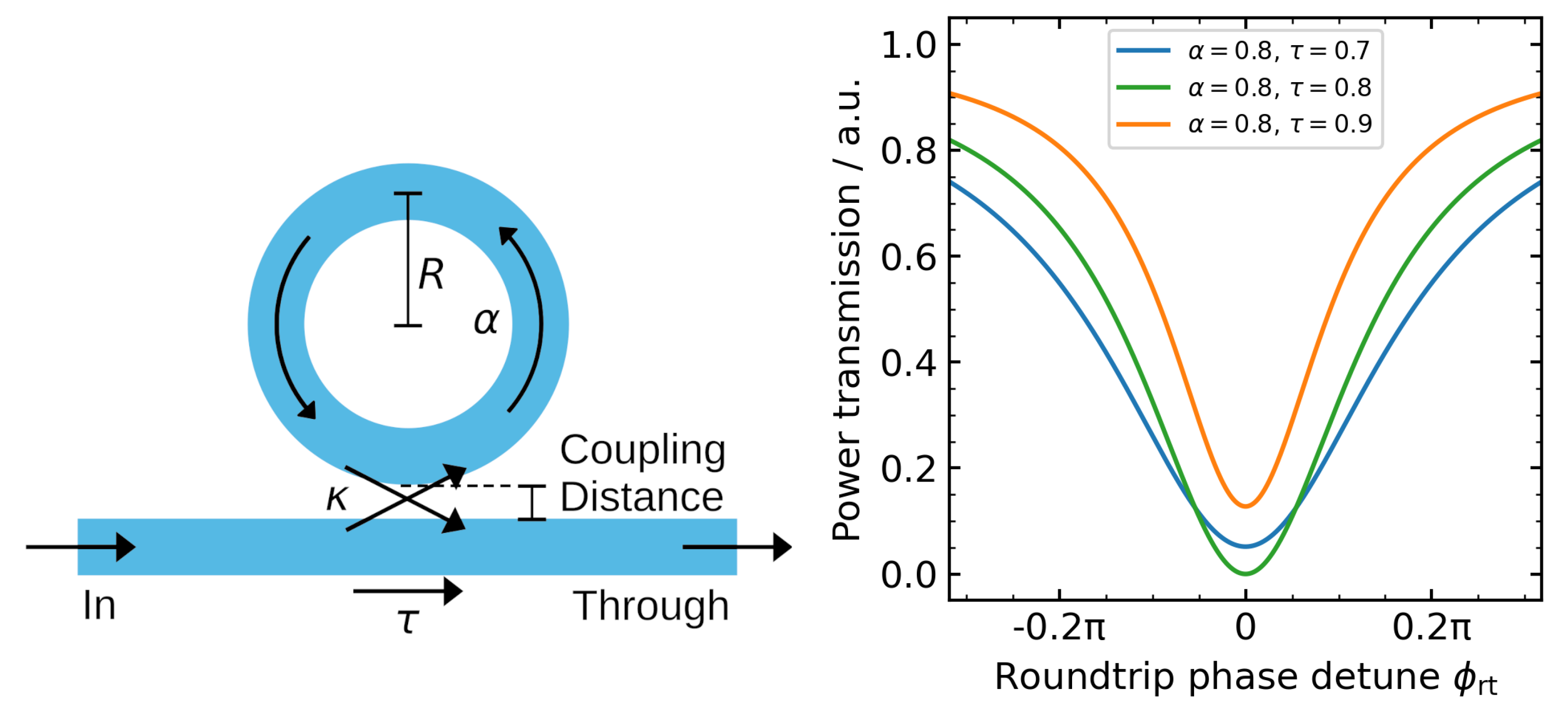
2. Coupling and Loss Coefficients of All-Pass Ring Resonators

Photonic all-pass ring resonators are self-contained waveguide structures. Light can be coupled into and out of the resonator evanescently via one bus waveguide. Depending on the irradiated wavelength and the optical path length, constructive interference can be realized inside the ring waveguide.
With wavelength λ , ring waveguide bend radius R, and effective refractive index of the waveguide n eff , the round-trip phase detune ϕ rt is given by:
ϕ rt = 4 π 2 R n eff λ
Assuming symmetrical coupling, the coupling between the ring and the bus waveguide is described by two coefficients: The cross-coupling κ is the part of the incident amplitude that couples from the bus waveguide into the ring waveguide (or vice versa). The self-coupling τ is the part of the incident amplitude that remains inside the bus waveguide (or the ring waveguide). For simplification, we assume loss-free coupling:
κ 2 + τ 2 = 1
Amplitude losses after a ring cycle are given by the loss coefficient [6]
α = exp 2 π R a
with the power attenuation coefficient a. For a loss-free resonator, α is unity.
The coupling coefficients τ and κ , as well as the loss coefficient α , determine the resonators response. They depend on the material stack and the waveguide geometry, but can be accessed through the design parameters coupling distance and length of the ring. Figure 1 shows a sketch of the configuration.
From the power transmission T at the all-pass resonators through port (normalized to the input power) [12]
T ( ϕ rt ) = τ 2 + α 2 2 τ α cos ( ϕ rt ) 1 + τ 2 α 2 2 τ α cos ( ϕ rt ) ,
one can deduce that for τ = α , the intensity at the through port is minimal (critical coupling).
Extracting coupling and loss coefficients can be achieved by obtaining values for the finesse F and extinction ratio E from measurements, as demonstrated in [8,9]. The analytical part of the method consists of two simple steps:
1.
Solve the equation of the finesse F for the product of τ α .
2.
Solve the equation of the extinction ratio E for a pair of values that can be allocated to τ , α .
Having derived equations for F and E from Equation (4), this yields [9]:
τ α = cos π F 1 + sin π F = A
τ , α = A E 1 A + E ± 1 E ± 1 A + E 1
Analytical differences found between [8,9] are due to implicit use of different definitions for the 3 dB bandwith. We utilize the definition
FWHM = λ res 2 2 π 2 R n g arccos 2 τ α 1 + τ 2 α 2
that is implicitly used by McKinnon et al. in [9] and is in line with the concept of defining the 3 dB bandwith as the bandwidth of the sum of all mode profiles [13]. In [8], they implicitly use a definition for the 3 dB bandwidth that is also given in [5], derived by setting the maximum transmission at the through port to unity. This is considered an approximation for weakly coupled, low-loss resonators. In terms of wavelength, this yields:
FWHM * = λ res 2 π 2 R n g arcsin 1 τ α 2 τ α
For weakly coupled, low-loss resonators, these definitions align well. It is noted in [14] that for specific applications or materials, the mismatch arising from the different expressions can become important; however, in case that the signal is normalized to unity, definitions from Equations (7) and (8) of course yield the same values.
Solving Equation (6) leaves an ambiguity in the assignment of the two values. This is because τ and α are symmetrical in Equation (4). McKinnon et al. [9] point out that for an all-pass resonator, the two individual values gained from Equation (6) can be assigned to τ or α through observation of their wavelength dependence, utilizing that the loss has a weaker dependence than the coupling coefficient. In our case, assignment is also possible through comparison of coefficients from resonators that differ only in their coupling distance.
Note also that if the device is probed close to the point of critical coupling, the assignment will switch with the resonator changing from over ( τ < α ) to undercoupled ( τ > α ) and vice versa depending on the wavelength.

3. Results

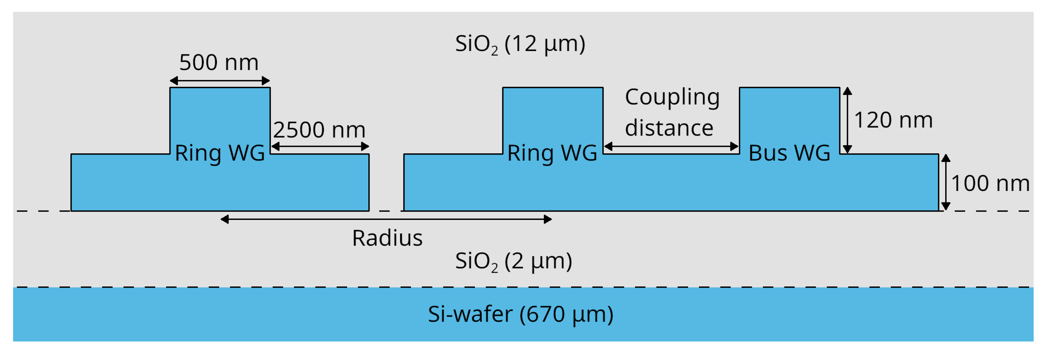
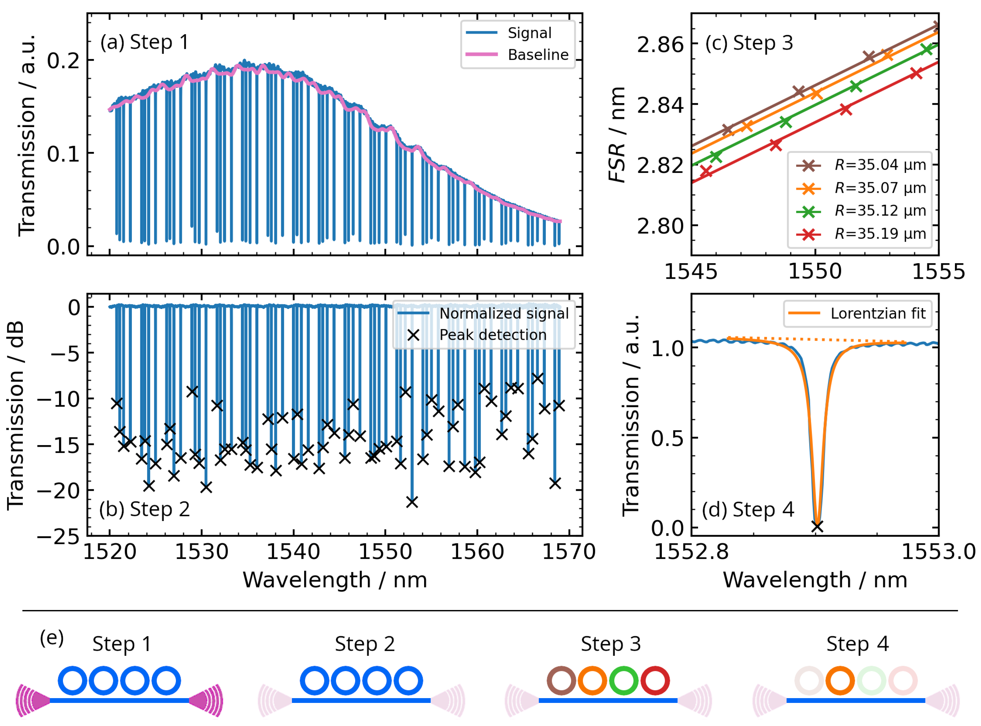
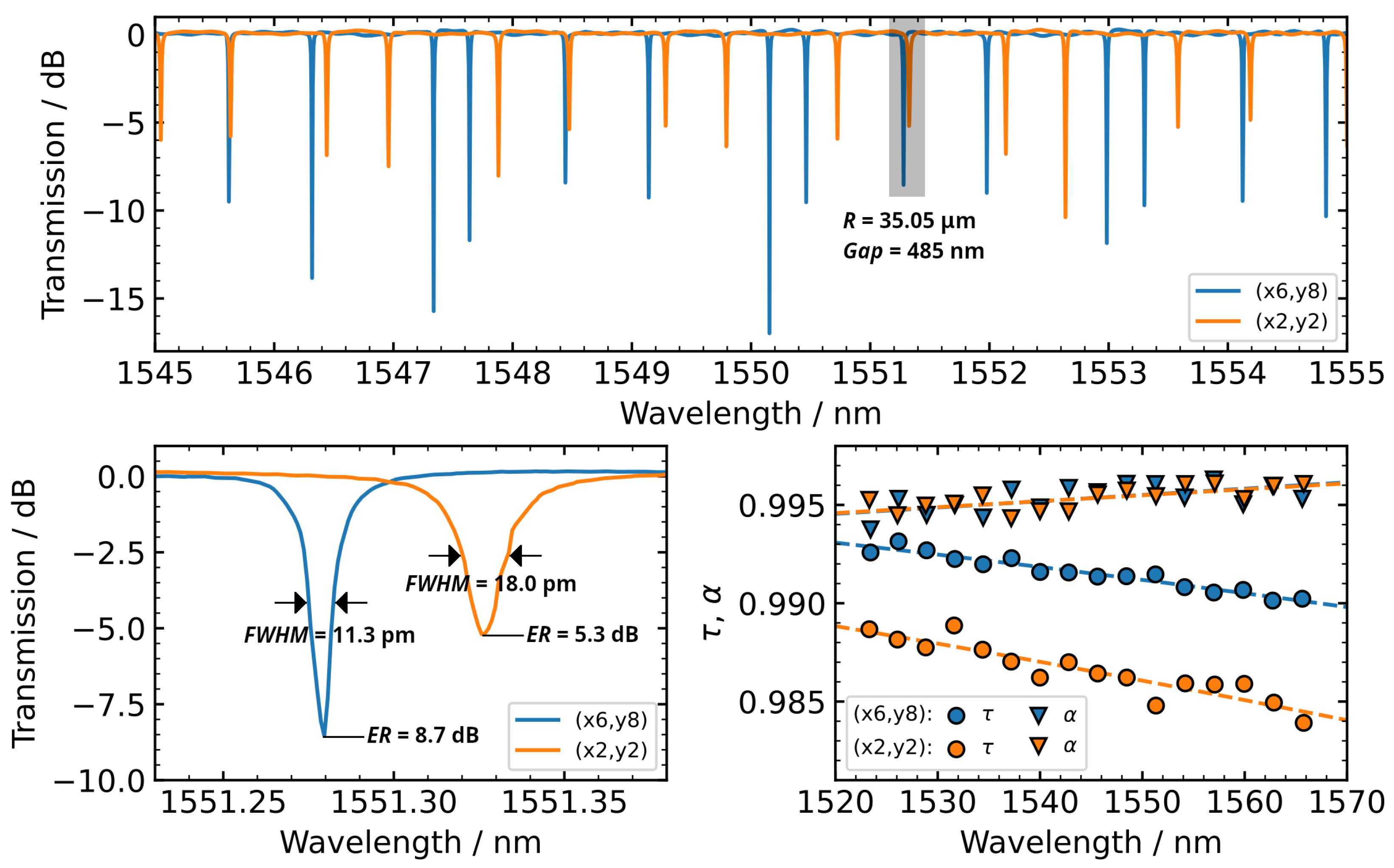
3.1. Experimental Setup and Data Processing

The measurements were performed using an automated wafer prober. A tunable laser (Keysight 81608A) was used as a source in combination with a Keysight N7745A photodiode. Recorded spectra spanned from 1520 nm to 1570 nm with a wavelength step size of 1 pm. Polarization was optimized using a Thorlabs FPC032 fiber polarization controller. Parallel to the photonic circuits, a reference gas cell (H13C14N) was probed to perform an in situ wavelength calibration. Next to a description of an experimental setup used for interrogating single chips, details on the calibration routine can be found in [15]. From 59 chips of a 200 mm wafer, a total of 2242 all-pass silicon ring resonators were probed. These 59 nominally identical photonic chips were manufactured on a multi-project wafer using IHP’s SG25H5_EPIC technology [16,17]. The waveguide geometry is a rib design in which the 220 nm high silicon is completely surrounded by silicon dioxide as depicted in Figure 2. Each photonic circuit consists of grating couplers that realize the fiber-to-chip coupling and multiple ring resonators which are serially coupled to the same bus waveguide (see Figure 3e). Three different ring radii of approximately 35 µm, 51 µm, and 70 µm were realized on each chip, with coupling distances ranging from 440 nm to 580 nm.
To effectively extract essential properties from the measured spectra, we implemented post-processing as follows. Figure 3a shows the spectrum of four serially coupled resonators with 35 µm radii with coupling distances from 510 nm to 540 nm. To compensate for the transfer function of the grating couplers, each spectrum was normalized to a baseline fitted with a low-pass filter (Figure 3a). After this, a simple peak detection of the normalized spectra is performed (Figure 3b). By design, each serially coupled resonator (coupled to the same bus waveguide) has a slightly different radius to ensure unique assignment of resonances and corresponding coupling distance by means of small differences in the free spectral range ( FSR , Figure 3c). We thereby assign the FSR to each resonant wavelength as the necessary positive wavelength shift to obtain a round-trip phase shift of 2 π [5]. For each determined peak, a lorentzian fit function (with linear background) is utilized (Figure 3d). From the lorentzian fit, we can immediately extract the resonance wavelength, the full width at half minimum, and the maximum and minimum transmission.

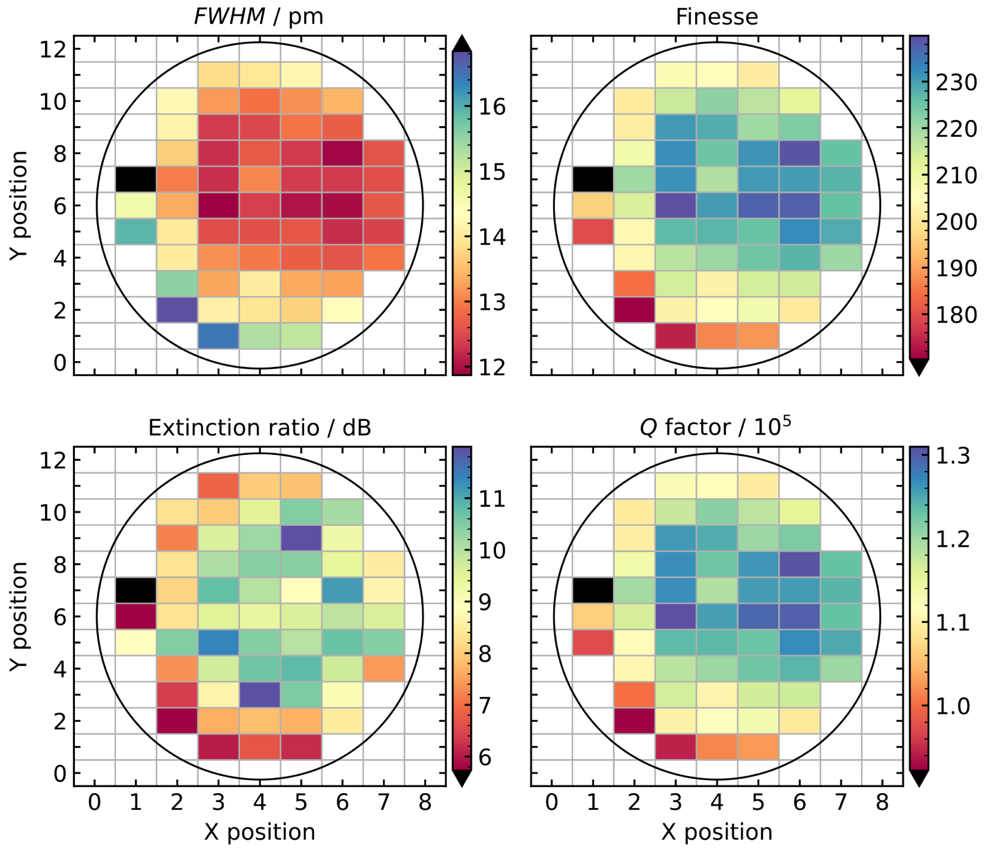
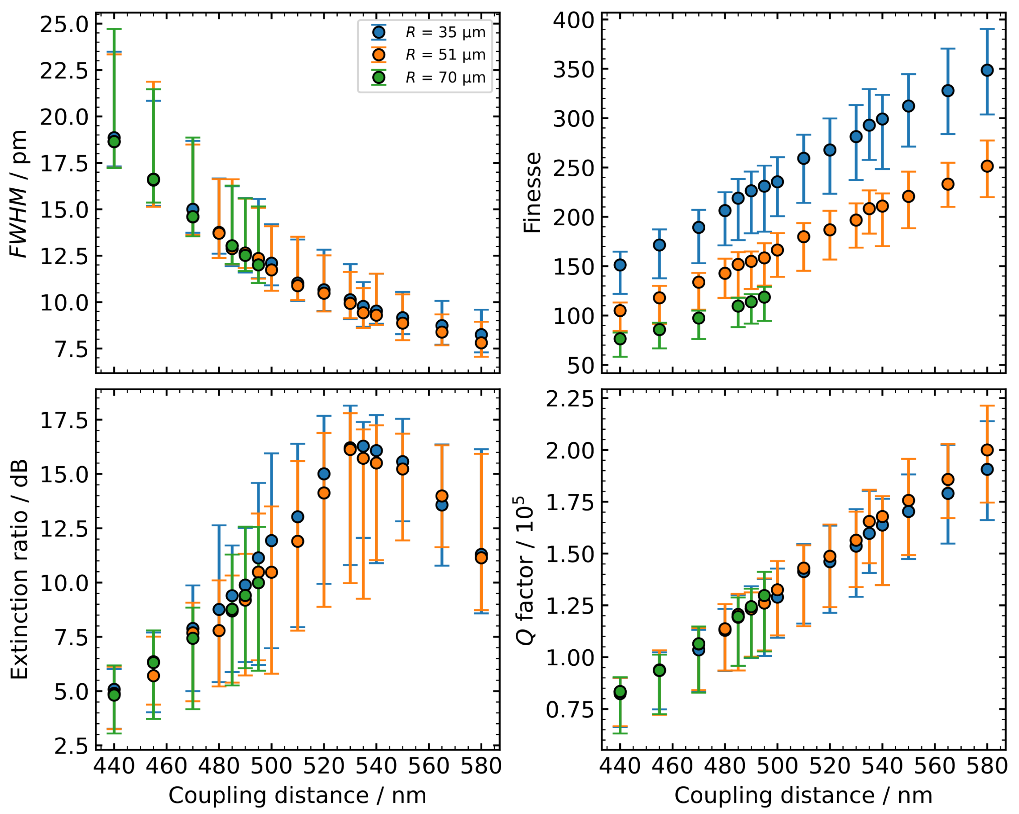
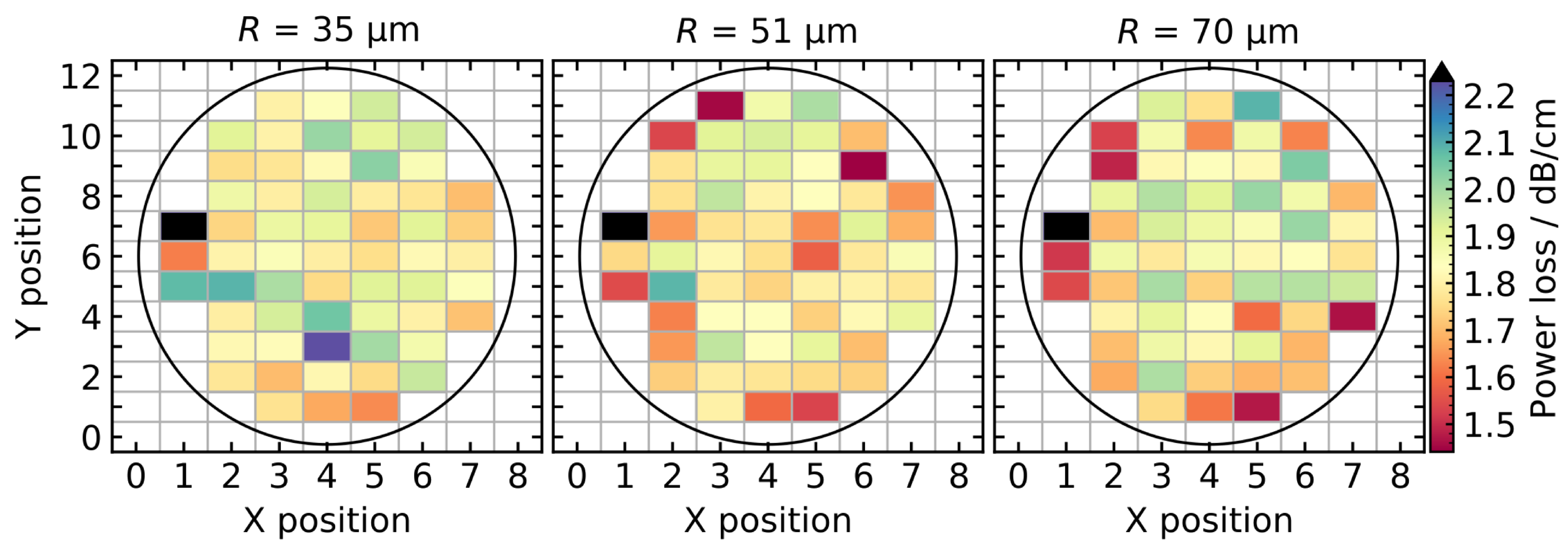
3.2. Wafer-Scale Optical Properties of Ring Resonators

Using the data extracted from the Lorentzian fit, we are able to determine the optical properties finesse, extinction ratio, and Q factor of all ring resonators at wafer-scale. Figure 4 exemplarily shows the results for ring resonators with a radius of 35 µm and a coupling distance of 485 nm. The color map represents the average value in the wavelength range from 1540 nm to 1560 nm, containing approximately 6 ( R = 35 µm), 10 ( R = 51 µm), or 20 ( R = 70 µm) resonances. The die at position x = 1 , y = 7 is considered an outlier and is not incorporated in the following evaluations.
In a first approximation, the optical properties show a radial spatial distribution over the wafer. Clearly, the central and right section of the wafer show a higher extinction ratio, Q factor, and finesse, and a smaller FWHM compared to the outer left part of the wafer. Inhomogeneous spatial distribution of material properties over a wafer is a common phenomenon related to multiple aspects of fabrication processes [11,18]. Reported spatial dependencies include refractive indices [19] and waveguide geometry [11,20].
Taking into account the dependence on the coupling distance, we can exploit our parameter sweep and present wafer-scale evaluation for each coupling distance in Figure 5. FWHM , finesse, and Q factor show monotonic behaviour depending on the coupling distance, whereas for resonators with radius of 35 µm and 51 µm, we can observe peak extinction ratios at coupling distances around 535 nm. For resonators with a radius of 70 µm, we have a smaller set of coupling distances ranging from 440 nm to 495 µm and that do not cross coupling regimes. For all of these properties, the variation across the wafer (whiskers in Figure 5) is asymmetric, reflecting the greater number of dies with properties close to the median in the central region of the wafer. With the exception of the extinction ratio, the span of variation is clearly dependent on the median, resulting in an almost constant relative variation. Figure 5 also shows that FWHM , Q factor, and extinction ratios barely depend on the ring radius. Only the finesse has the expected radius dependence, resulting from the different values of the free spectral range.
Beyond the applied approach of averaging optical properties over the wavelengths from 1540 nm to 1560 nm, we can report the highest 2.5 % of measured Q factors for resonators with R = 35 µm to be within a range from 213,000 to 273,000 and the highest 2.5 % values for the extinction ratio to be within a range from 18.9 dB to 26.1 dB. The extinction ratio is maximised at coupling distances where critical coupling is achieved and only limited by stray light [9]. In contrast, the Q factor is limited by the investigated range of coupling distances. At the cost of a lower extinction ratio, achieving higher Q factors would be possible with larger coupling distances.

3.3. Coupling and Loss

In the following, intra-wafer variations of coupling and loss and the effect of varying coupling distances on coupling coefficients are determined experimentally. As described in Section 2, the difference in resonance spectra (e.g., extinction ratio and 3 dB bandwidth) of nominally identical resonators from different dies on the wafer can be explained by their coupling and loss coefficients. Figure 6 shows a clear example of these differences for nominally identical resonators with R = 35 µm and coupling distance of 485 nm from a chip near the centre of the wafer (position x = 6 , y = 8 , refer to Figure 4) and one from the edge (position x = 2 , y = 2 ). The center wavelength of the resonances differs between the two dies due to different optical path lengths. These variations extend over at least the free spectral range, and therefore quantification is unfeasible without knowledge of the resonance order. The coupling and loss coefficients shown in Figure 6 over a range of 50 nm are extracted as described in Section 2. The loss coefficient does not differ and the reason for the different shapes of the resonance spectra is due to different coupling strengths. For interpolation, fit functions [9] with free parameters a 0 to a 3 are used:
τ λ = | cos a 0 + a 1 λ |
α λ = a 2 + a 3 λ
By applying the formalism from Section 2 to the processed data of the 59 nominally identical chips (see sections above), we can calculate wafer maps for coupling and loss coefficients as depicted in Figure 7. As these coefficients are wavelength dependent, we utilize the values of the fit functions (see Figure 6 bottom right) at λ = 1550 nm as a reference value. The values in Figure 7 are normalised to the median of all 59 dies to show their relative variations (for the loss coefficient, the die at position x = 1 , y = 7 is an outlier and is not included). At wafer-scale, the coupling coefficient τ varies more strongly than the loss coefficient α , as already observed for two dies in Figure 6. Moreover, in a first approximation, the loss coefficient is randomly distributed over the wafer, whereas the coupling coefficient shows radial dependence with weaker coupling around the center and stronger coupling towards the edges of the wafer. It can thus be deduced that the intra-wafer variations of optical properties found in Section 3.2 are mainly caused by variations in coupling strength.
As a benchmark, we compare the loss values calculated above with the waveguide loss of approximately 1.5 dB/cm obtained from test structures on the same wafer. A total of 95% of the losses deduced from α are in the range from 1.78 dB/cm to 2.14 dB/cm ( R = 35 µm), 1.66 dB/cm to 1.99 dB/cm ( R = 51 µm), and 1.59 dB/cm to 1.94 dB/cm ( R = 70 µm), which is in good agreement with the standard waveguide loss. As in Equation (2) we assumed loss-free coupling, α includes waveguide propagation losses, bending losses, and coupling losses [6], and as such is expected to be slightly higher. The distribution of losses in dB/cm over the wafer can be found in Figure 8.
In Figure 9, we analyse the coupling and loss coefficients as a function of coupling distance to determine the coupling distance at which critical coupling ( α = τ ) occurs. The coefficients of resonators with radii of 35 µm, 51 µm, and 70 µm from 58 dies are represented by the median (dots, triangles) and 95% span (whiskers). The green histogram shows the underlying distribution of coupling coefficients for resonators of 70 µm radius at a coupling distance of 490 nm as an example, reflecting the distribution from Figure 7.
To derive a coupling distance that realises critical coupling, we incorporated two fitting functions for the coefficients and determined the distance at which they intersected. As for the loss coefficient, we did not find a clear dependence on the coupling distance; thus, we used a constant function. For the coupling coefficient, we utilized the following expression with the coupling distance g and parameters b 0 and b 1 :
τ g = 1 b 0 exp g · b 1
Applying these fits to resonators from 58 dies, we obtained an asymmetrical distributed set of fit functions representing the individual coupling and loss coefficients (median depicted as colored line and 95% span as areas in Figure 9). The resulting distribution of intersection points where α = τ , representing the optimal coupling distances for critical coupling, is shown for resonators of 35 µm radius in the blue histogram in Figure 9. From these distributions of the three radii, the median (solid lines) and the 95% range (dashed lines) were calculated, and their values are shown at the top of the graph. A total of 95 % of coupling distances that realized critical coupling are within a range from 531 nm to 588 nm ( R = 35 µm), 535 nm to 590 nm ( R = 51 µm), and 543 nm to 601 nm ( R = 70 µm). Figure 9 also shows that both τ and α depend on the radius of the resonator. The loss inside the ring waveguide accumulates over its length and the coupling region increases with an increasing radius. For resonators with a radius of approximately 70 µm, critical coupling was not reached within the given range of coupling distances. Nonetheless, curve fitting allows for extrapolation to infer a coupling distance at which τ = α . The ability to predict values for τ and α outside of the realized parameter range is further investigated in the following Section 3.4.

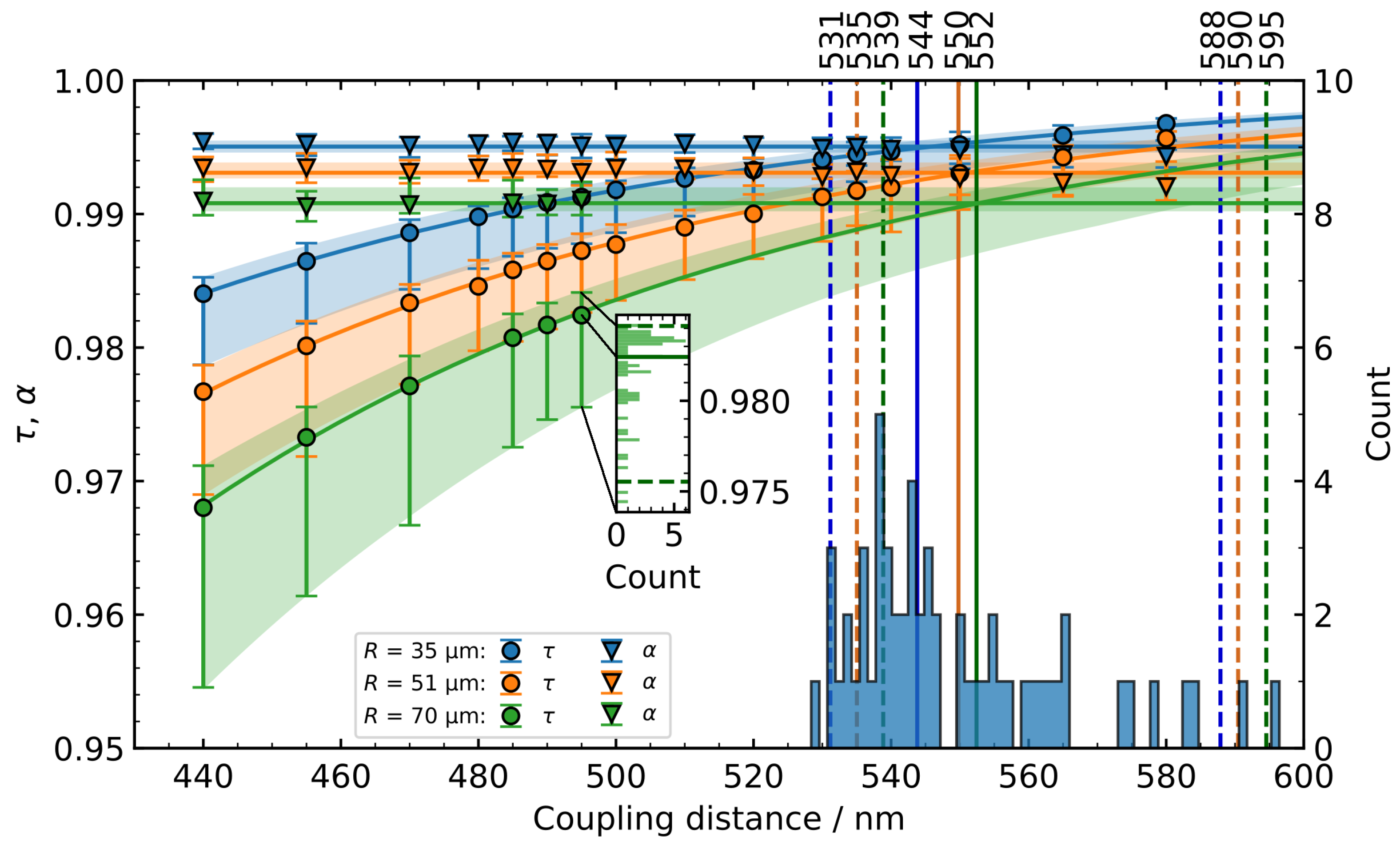
3.4. Prediction of Coupling Coefficients from a Reduced Set of Parameters

The ability to predict values for τ and α outside of a realized parameter range is beneficial for optimizing the performance of resonators based on a small set of test structures. It should be noted that one can also use the extinction ratio versus the coupling distance as a measure to infer the coupling regime (critically coupled, under, or overcoupled), as it shows non-monotinic behaviour. Practically, this is only possible if the investigated set of coupling distances does incorporate the transition between the mentioned regimes. As demonstrated in Section 3.3 (see Figure 9), the utilization of fit functions for coupling and loss coefficients depending on the coupling distance allows for extrapolation, regardless of whether the set of investigated coupling distances spans over the different regimes.
To investigate this method quantitatively, we chose the resonators with radii of approximately 35 µm on the chip that has its intersection point of τ and α closest to the median of all intersection points (and is the central chip on the wafer at position x = 4 , y = 6 ). For a given number of coupling distances (see Figure 10), we draw all possible combinations of coupling distance values g, or 1000 unique random combinations if the set of possible combinations exceeds 1000. For these parameter sets, curve fitting is used ( α ( g ) constant and τ ( g ) from Equation (11)) to obtain values for the coupling distances where τ ( g ) = α ( g ) . Figure 10 shows the results as a violin plot, using a Gaussian kernel density estimation to represent the underlying distribution. The whiskers contain 95 % of the data. These results are compared to the median (solid line) and 95 % interval (dashed lines) of intersection points introduced in Figure 9 from wafer-scale statistics.
As expected, the results converge as the number of coupling distance values used for the prediction of the critical coupling distance increases. According to our results, even for only three coupling distances, 95 % of the predicted values are within the 95 % interval derived from the wafer-scale statistics. This means that this prediction accuracy may already be sufficient, as it is within the variation on wafer level. Of course, coupling distances that are spread more evenly over the investigated range will give more accurate predictions, and values far away from critical coupling will lead to less accurate predictions. However, the results suggest that with a coarse simulation as a starting point, a small number of coupling distance test parameters may be sufficient to predict coupling coefficients and optimise design parameters.

4. Discussion

We presented a wafer-scale analysis of the 3 dB bandwidth, finesse, Q factor, and extinction ratio for silicon all-pass ring resonators. This investigation was based on spectra of 2242 resonators from 59 nominally identical dies of a 200 mm wafer. The probed resonators were of three different radii and 16 different coupling distances. We found the highest 2.5 % of Q factors and extinction ratios to be larger than 213,000 and 18.9 dB. Averaging over resonances between wavelengths from 1540 nm to 1560 nm we found monotonic dependence of the 3 dB bandwidth, finesse, and Q factor on the coupling distance. For resonators with a radius of 35 µm and 51 µm, we found peak extinction ratios at coupling distances around 535 nm, indicating critical coupling.
For every coupling distance, we were able to give the intra-wafer variations of these properties, which were found to be asymetrically distributed. Using the resonators’ transfer function, we were able to extract coupling and loss coefficients ( τ , α ) for every resonator. For the coupling coefficient, we found a nonlinear dependence on the coupling distance, whereas the loss coefficient was almost constant (depending only on the radius). Additionally, we found intra-wafer variations to be more present in the coupling coefficient than the loss coefficient, both being asymetrically distributed. Spatially, the variations in loss seem randomly distributed over the wafer, and the coupling coefficient shows spatial dependence, indicating weaker coupling around the center of the wafer. As the same spatial distribution was observed for the optical properties, we deduce that these variations are caused by variations in coupling strength. Referencing the detailed descriptions given in [11], we can categorize the variations found in our research into intra-wafer random (loss coefficient) and intra-wafer systematic (coupling coefficient). It is likely that the coupling fluctuates because of variations in waveguide geometry. Both the thickness and width of the waveguides depend on systematic variations, e.g., polishing of the SOI wafer and spin coating and etching processes. Random variations introduced by the lithographic process likely have an effect on the width. Investigation of the correlation between fabrication process, waveguide geometry, and the measurement data is beyond the scope of this work, but will be pursued in the future.
Using curve fitting to describe the relation between the coefficients and the coupling distance, we found critical coupling at intersection points where τ = α . To the exclusion of a die that was considered an outlier, we found the span of distances containing 95 % of the intersection points on the wafer to be as large as 60 nm. We used this method also for the resonators with a radius of 70 µm, for which we did not observe peak extinction ratio within the given range of coupling distances. The fit functions enabled us to infer intersection points ( τ = α ) through extrapolation, thus predicting coupling distances that realize critical coupling.
We further analysed the use of curve fitting as a tool to predict coupling and loss coefficients outside of an experimentally investigated parameter range. The previous wafer-scale investigation of these coefficients served us as a benchmark for this analysis. Based on different numbers of coupling distances, we predicted distances that realize critical coupling. Comparing the results with the values gained from wafer-scale investigation, we found that within our parameter range, three gaps are already sufficient, so that 95 % of the predicted values fall within the 95 % interval derived from intra-wafer variation. We consider this method an efficient way to identify coupling regimes and design parameters that realize a desired performance. As high-accuracy applications targeting optimal design parameters can require testing hundreds of different configurations, our investigation exemplifies an efficient pathway for future parameter sweeps. Given premised fabrication within the same process, successive designs can thus converge quickly towards an optimized design with test structures requiring a smaller footprint.
A change in fabrication process will likely result in offsets for loss and coupling coefficients and change the span of intra-wafer variations. The presented methods are of universal nature, e.g., the ability to predict coupling distances that realize a desired performance is not subject to the type of process. Investigation of photonic circuit yield is still in its infancy, but a more widespread use of grating couplers in recent years allows the probing of circuits without cleaving and thus enables the determination of intra-wafer variations with more ease. For high-accuracy applications, e.g., in the field of metrology [21], knowledge of these variations is vital. We encourage future research to illuminate these variations for a wide range of advanced photonic components as they are critical for the dissemination of integrated photonics.

Author Contributions

Conceptualization, D.S., R.E. and S.K.; software, D.S. and R.E.; analysis and visualization, D.S.; resources, G.W. and L.Z.; investigation, A.P.; writing, D.S., R.E. and S.K.; supervision, S.K. and L.Z. All authors have read and agreed to the published version of the manuscript.

Funding

This work was partly carried out within the framework of the projects PhotOQuant (17FUN05), which has received funding from the EMPIR programme, co-financed by the Participating States and from the European Union’s Horizon 2020 research and innovation programme; and PhoQuS-T (23FUN01), which has received funding from the European Partnership on Metrology, co-financed from the European Union’s Horizon Europe Research and Innovation Programme and by the Participating States.

Data Availability Statement

Data underlying the results presented in this paper are not publicly available at this time but may be obtained from the authors upon reasonable request.

Conflicts of Interest

The authors declare no conflicts of interest.

References

  1. Liu, D.; Xu, H.; Tan, Y.; Shi, Y.; Dai, D. Silicon photonic filters. Microw. Opt. Technol. Lett. 2021, 63, 2252–2268. [Google Scholar] [CrossRef]
  2. Chen, X.; Lin, J.; Wang, K. A Review of Silicon-Based Integrated Optical Switches. Laser Photonics Rev. 2023, 17, 2200571. [Google Scholar] [CrossRef]
  3. Kazanskiy, N.L.; Khonina, S.N.; Butt, M.A. A Review of Photonic Sensors Based on Ring Resonator Structures: Three Widely Used Platforms and Implications of Sensing Applications. Micromachines 2023, 14, 1080. [Google Scholar] [CrossRef] [PubMed]
  4. Zhao, B.; Cheng, J.; Wu, B.; Gao, D.; Zhou, H.; Dong, J. Integrated photonic convolution acceleration core for wearable devices. Opto-Electron. Sci. 2023, 2, 230017. [Google Scholar] [CrossRef]
  5. Van, V. Optical Microring Resonators: Theory, Techniques, and Applications; Series in Optics and Optoelectronics; CRC Press: Boca Raton, FL, USA, 2016. [Google Scholar]
  6. Bogaerts, W.; De Heyn, P.; Van Vaerenbergh, T.; De Vos, K.; Kumar Selvaraja, S.; Claes, T.; Dumon, P.; Bienstman, P.; Van Thourhout, D.; Baets, R. Silicon microring resonators. Laser Photonics Rev. 2012, 6, 47–73. [Google Scholar] [CrossRef]
  7. Rabus, D.G. Ring resonators: Theory and modeling. In Integrated Ring Resonators: The Compendium; Springer: Berlin/Heidelberg, Germany, 2007; pp. 3–40. [Google Scholar]
  8. Scheuer, J.; Yariv, A. Fabrication and characterization of low-loss polymeric waveguides and micro-resonators. J. Eur. Opt. Soc. Rapid Publ. 2006, 1, 06007. [Google Scholar] [CrossRef]
  9. McKinnon, W.R.; Xu, D.X.; Storey, C.; Post, E.; Densmore, A.; Delâge, A.; Waldron, P.; Schmid, J.H.; Janz, S. Extracting coupling and loss coefficients from a ring resonator. Opt. Express 2009, 17, 18971–18982. [Google Scholar] [CrossRef] [PubMed]
  10. Twayana, K.; Ye, Z.; Helgason, Ó.B.; Vijayan, K.; Karlsson, M.; Torres-Company, V. Frequency-comb-calibrated swept-wavelength interferometry. Opt. Express 2021, 29, 24363–24372. [Google Scholar] [CrossRef] [PubMed]
  11. Xing, Y.; Dong, J.; Khan, U.; Bogaerts, W. Capturing the Effects of Spatial Process Variations in Silicon Photonic Circuits. ACS Photonics 2022, 10, 928–944. [Google Scholar] [CrossRef]
  12. Yariv, A. Universal relations for coupling of optical power between microresonators and dielectric waveguides. Electron. Lett. 2000, 36, 321–322. [Google Scholar] [CrossRef]
  13. Ismail, N.; Kores, C.C.; Geskus, D.; Pollnau, M. Fabry-Pérot resonator: Spectral line shapes, generic and related Airy distributions, linewidths, finesses, and performance at low or frequency-dependent reflectivity. Opt. Express 2016, 24, 16366–16389. [Google Scholar] [CrossRef] [PubMed]
  14. Yang, Q. Finesse of ring resonators. AIP Adv. 2023, 13, 085225. [Google Scholar] [CrossRef]
  15. Eisermann, R.; Krenek, S.; Winzer, G.; Rudtsch, S. Photonic contact thermometry using silicon ring resonators and tuneable laser-based spectroscopy. Tm-Tech. Mess. 2021, 88, 640–654. [Google Scholar] [CrossRef]
  16. Zimmermann, L.; Knoll, D.; Kroh, M.; Lischke, S.; Petousi, D.; Winzer, G.; Yamamoto, Y. BiCMOS Silicon Photonics Platform. In Proceedings of the Optical Fiber Communication Conference, Los Angeles, CA, USA, 22–26 March 2015; Optica Publishing Group: Washington, DC, USA, 2015; p. Th4E.5. [Google Scholar] [CrossRef]
  17. Michalik, P.; Fernández, D.; Wietstruck, M.; Kaynak, M.; Madrenas, J. Experiments on MEMS Integration in 0.25 µm CMOS Process. Sensors 2018, 18, 2111. [Google Scholar] [CrossRef] [PubMed]
  18. Siew, S.; Li, B.; Feng, G.; Zheng, H.; Zhang, W.; Guo, P.; Xie, S.; Song, A.; Dong, B.; Luo, L.; et al. Review of Silicon Photonics Technology and Platform Development. J. Light. Technol. 2021, 39, 4374–4389. [Google Scholar] [CrossRef]
  19. Butt, J.N.; Tyndall, N.F.; Pruessner, M.W.; Walsh, K.J.; Miller, B.L.; Fahrenkopf, N.M.; Antohe, A.O.; Stievater, T.H. Optical and geometric parameter extraction across 300-mm photonic integrated circuit wafers. APL Photonics 2024, 9, 016104. [Google Scholar] [CrossRef]
  20. Boynton, N.; Pomerene, A.; Starbuck, A.; Lentine, A.; DeRose, C.T. Characterization of systematic process variation in a silicon photonic platform. In Proceedings of the 2017 IEEE Optical Interconnects Conference (OI), Santa Fe, NM, USA, 5–7 June 2017; pp. 11–12. [Google Scholar] [CrossRef]
  21. Dedyulin, S.; Ahmed, Z.; Machin, G. Emerging technologies in the field of thermometry. Meas. Sci. Technol. 2022, 33, 092001. [Google Scholar] [CrossRef]
Figure 1. Left: Schematic of an all-pass ring resonator with radius R, amplitude losses α , amplitude coupling coefficients τ , κ and a coupling distance between ring and bus waveguide. Right: Impact of coupling and loss coefficients on the all-pass resonators lineshape.
Photonics 12 00234 g001
Figure 2. Cross section of the rib waveguide (WG) geometry under investigation (not to scale). Radii of approximately 35 µm, 51 µm, and 70 µm were realized, with coupling distances ranging from 440 nm to 580 nm.
Photonics 12 00234 g002
Figure 3. Data processing steps of the spectrum of four serially coupled all-pass resonators: (a) Spectrum is normalized to the transfer function of the grating couplers fitted by a low-pass filter. (b) Detection of local minima. (c) Assignment of individual resonances through a unique free spectral range. The FSR is assigned to each resonant wavelength (colored cross) in positive direction and curve fitted using a linear function. (d) Fitting with Lorentzian function and linear background for all minima. (e) Visualisation of the processing steps with regard to components of the integrated circuit: Step 1 represents the whole circuit, Step 2 has the grating couplers transfer function filtered, Step 3 enables the association of each resonance to an individual resonator, and Step 4 extracts the response of individual rings.
Photonics 12 00234 g003
Figure 4. Wafer mapping of a 200 mm wafer for optical properties averaged over resonances between wavelengths from 1540 nm to 1560 nm for resonators with a radius of approximately 35 µm and coupling distance of 485 nm. The die at position x = 1 , y = 7 is considered an outlier.
Photonics 12 00234 g004
Figure 5. Wafer-scale evaluation of FWHM , finesse, extinction ratio, and Q factor averaged over wavelengths from 1540 nm to 1560 nm for resonators with radii of 35 µm, 51 µm, and 70 µm versus the coupling distance. Markers represent the median values of 58 dies of the wafer, whiskers contain 95 % of the data.
Photonics 12 00234 g005
Figure 6. Top: Spectra from two nominally identical circuits, each containing 4 resonators each with radii of approximately 35 µm and coupling distances within the range of 485 nm to 500 nm from different positions on the wafer (refer to Figure 4). Shaded region is magnified in the bottom left part of the figure. Bottom Left: Shapes of resonances of two nominally identical resonators with R = 35.05 µm and coupling distance of 485 nm from different positions on the wafer, showcasing FWHM and extinction ratio ( E R ). Bottom Right: Coupling and loss coefficients of these resonators in the wavelength range from 1520 nm to 1570 nm, with dashed lines from fit functions (Equations (9) and (10)).
Photonics 12 00234 g006
Figure 7. Wafer mapping of a 200 mm wafer for coupling and loss coefficients at λ = 1550 nm for different radii and coupling distance of 485 nm. Values are normalized to the median (red cross). For the loss coefficient, the die at position x = 1 , y = 7 is considered an outlier.
Photonics 12 00234 g007
Figure 8. Wafer mapping of a 200 mm wafer for power loss in dB/cm derived from the resonators’ loss coefficients at λ = 1550 nm for different radii with coupling distance of 485 nm. The die at position x = 1 , y = 7 is considered an outlier.
Photonics 12 00234 g008
Figure 9. Coupling and loss coefficients of resonators with radii of approximately 35 µm, 51 µm, and 70 µm versus the coupling distance from 58 dies. Median values are indicated by the markers. The whiskers contain 95 % of the data. Calculating fit functions for each die on the wafer individually results in the colored areas, representing the span of 95 % of the fit functions. The vertical histogram (green) shows the asymmetrical distribution of coupling coefficients over the wafer (for resonators with radius of approximately 70 µm). Through the fit functions, we obtain intersection points where α = τ . The distribution of these intersection points is represented by the horizontal histogram (blue) for resonators with a radius of approximately 35 µm. Solid lines represent the median of the distributions, dashed lines represent the corresponding span of 95 % of the data.
Photonics 12 00234 g009
Figure 10. Predicted coupling distances for critical coupling based on intersection points of fit functions for coupling and loss coefficients. The violin plot represents the underlying distribution and whiskers contain 95 % of the data. We implement the median (solid line) and 95 % interval (dashed lines) of intersection points from the wafer-scale statistics introduced in Figure 9.
Photonics 12 00234 g010
Disclaimer/Publisher’s Note: The statements, opinions and data contained in all publications are solely those of the individual author(s) and contributor(s) and not of MDPI and/or the editor(s). MDPI and/or the editor(s) disclaim responsibility for any injury to people or property resulting from any ideas, methods, instructions or products referred to in the content.

