Abstract
Entangled photons are essential for photonic quantum technologies. Their generation typically relies on spontaneous parametric down-conversion, but conventional nonlinear crystals are bulky and hard to integrate on chips. Rhombohedral-stacked MoS2 combines a high refractive index, large second-order nonlinearity, and flexibility for heterogeneous integration, making it a promising platform for integrated quantum photonics. However, the typical thin-film form of 3R-MoS2 restricts the effective nonlinear interaction length, limiting entanglement generation efficiency in practical devices. To overcome this, phase-matching strategies in integrated waveguides are required but have so far remained undeveloped. Here, we introduce a waveguide-integrated 3R-MoS2 platform with periodic grooves to achieve quasi-phase matching, enhancing down-conversion efficiency. Leveraging tensor symmetries and orthogonal waveguide modes, the design efficiently generates entangled photons, providing a compact, scalable route toward 2D-material-based integrated quantum photonic circuits.
1. Introduction
Entangled photons are fundamental resources for quantum technologies, underpinning applications in communication, computation, and sensing. They can be generated either from quantum emitters, such as atoms [1] and quantum dots [2,3,4], or through nonlinear optical processes in bulk materials or on integrated platforms [5,6]. Among these approaches, spontaneous parametric down-conversion (SPDC), a second-order nonlinear process, remains the most widely used method for producing polarisation-entangled photons. Conventional bulk crystals such as BBO and KTP have been extensively employed [7,8], but their large dimensions and limited compatibility with photonic integration hinder the development of scalable and compact quantum circuits [9,10].
Rhombohedral-stacked two-dimensional (2D) materials, exemplified by 3R-MoS2, have recently emerged as a promising new class of nonlinear media for integrated quantum photonics [11,12,13,14,15]. Unlike conventional bulk crystals, they combine a high refractive index for strong light confinement with a large second-order nonlinearity (∼100–800 pm/V) and intrinsic compatibility with chip-scale integration [15,16,17,18]. Wafer-scale growth of homogeneous rhombohedral films has now been demonstrated [19,20,21], strengthening their prospects for scalable photonic devices. Entangled photon pairs have already been realised, with tunability between different Bell states enabled by in-plane crystal symmetries [22,23,24]. Nevertheless, the limited thickness of 3R-MoS2 (typically a few hundred nanometres) constrains the effective nonlinear interaction length. While such thin films do not generally require phase matching, the short interaction length still leads to modest conversion efficiency, albeit substantially higher than in monolayers. To achieve further enhancement, extending the interaction length in waveguide or cavity geometries will require effective phase-matching strategies [25,26,27]. Such phase-matching strategies have so far remained undeveloped in integrated 3R-MoS2 waveguides.
Here, we introduce a waveguide-integrated 3R-MoS2 platform that employs periodic grooves to realise quasi-phase matching (QPM). This approach modulates the effective refractive index along the propagation direction, compensating phase mismatch and markedly improving down-conversion efficiency. By leveraging the tensor symmetries of 3R-MoS2, the design utilises orthogonal electric field components in different waveguide modes for entangled-photon generation. Our design offers a practical pathway toward compact, high-performance entangled-photon sources in 2D materials, advancing their integration into scalable quantum photonic circuits.
2. Design Strategy
We first focus on the principle of parametric down-conversion in 3R-MoS2 and outline our design strategy. In rhombohedral MoS2, the S–Mo–S monolayers are stacked in a translationally shifted sequence (ABC stacking, see Figure 1a), without the 180° rotations that appear in the 2H phase. This stacking breaks inversion symmetry along the vertical (out-of-plane, labelled y, Figure 1b) direction even for multilayer or thick 3R-MoS2, allowing a non-zero second-order nonlinear susceptibility, , to persist with increasing thickness. The crystal belongs to the non-centrosymmetric point group . In this symmetry, the dominant non-vanishing tensor components [18,22] are , which couple primarily to the in-plane electric field components (, ), whereas contributions involving the out-of-plane field () are typically much weaker.
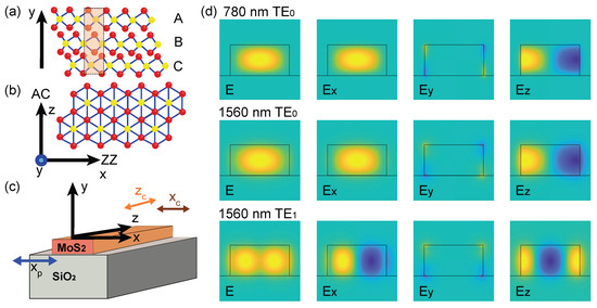
Figure 1.
The strip waveguide design. (a,b) Atomic structure of 3R-MoS2. A, B, and C indicate the lateral positions of successive layers, forming an ABC–ABC stacking sequence distinct from the AB–AB stacking of 2H-MoS2. The y-axis is defined along the vertical stacking direction, while the x–z plane coincides with the MoS2 surface, aligned with the armchair (AC) and zigzag (ZZ) crystal directions. The dominant non-vanishing tensor components lie within the x–z plane. (c) Schematic of the 3R-MoS2 thin film in a strip-waveguide geometry. The z-axis represents the propagation direction, and the x–y plane corresponds to the cross-sectional view. (d) Electric field distributions and their projections along the x, y, and z axes for the TE0 (780 nm), TE0 (1560 nm), and TE1 (1560 nm) modes, respectively. The mode profiles are calculated using a finite-difference eigenmode (FDE) solver in Lumerical MODE. Yellow, cyan, and blue indicate positive, zero, and negative field amplitudes, respectively.
The symmetry of the tensor underpins the generation of polarisation-entangled photon pairs. In the SPDC process, an x-polarised pump photon can produce either – photon pairs via or – pairs via (where the subscripts s and i denote the signal and idler photons), with the same principle applying to a z-polarised pump. This enables a coherent superposition, yielding the entangled state under an x-polarised pump. These tensor properties have important implications for integrated device design, as the polarisation-dependent coupling must be carefully controlled. In particular, the down-converted photons must be coupled to orthogonal electric field components—if one photon couples to , the other must couple to —necessitating separate mode design.
Efficient nonlinear energy conversion further requires satisfying the phase-matching condition for propagation in waveguides, with . For practical applications in quantum communication, we target entangled-photon generation in the telecom band around 1560 nm. At this wavelength, the intrinsic material absorption is negligible [12]. However, achieving phase matching in 3R-MoS2 is challenging due to its strong birefringence and material dispersion. The optical axis lies along the y direction, with refractive indices [12] of and at 780 nm, while at 1560 nm decreases to ≈4.1 and remains nearly constant. These material properties preclude straightforward birefringent phase matching in the waveguide, necessitating alternative strategies to achieve high-efficiency entangled photon-pair generation.
3. Strip Waveguide Design
We first consider a simple rectangular (strip) waveguide of 3R-MoS2 that is transferred on a SiO2 substrate. The effective refractive index is modified by the modal distribution of the waveguide, which in turn affects the wavevectors.
The waveguide cross-section is aligned with the material’s x–y plane, with the z-axis defined as the propagation direction (Figure 1c). Note that the coordinate system follows that in Figure 1a,b, where the y-axis corresponds to the ABC stacking direction (vertical thickness). In this configuration, the SPDC process follows the notation introduced earlier: , where the pump and entangled photons are at 780 nm and 1560 nm (degenerate), respectively. At a given position , the SPDC efficiency is determined by the transverse overlap of the electric fields, , where the superscripts p, c denote the pump and down-converted photons, respectively, and the integral is taken over the waveguide cross-section. The design therefore aims to select modes at 1560 nm with strong and components to maximise the nonlinear overlap while keeping the entangled photons in separable orthogonal modes.
The electric field distribution of the fundamental TE0 mode at the pump wavelength of 780 nm was analysed within this waveguide (Figure 1d, first row). The results show that the electric field is dominated by the x-component (), while the z-component is much weaker and exhibits odd symmetry along the x-direction, and the y-component is negligible. A similar distribution is obtained for the fundamental TE0 mode at the conversion wavelength of 1560 nm, except that the confinement at this longer wavelength is slightly weaker, leading to a broader spatial extent of the mode profile and slightly reduced field intensity in the waveguide region (Figure 1d, second row).
The third row of Figure 1d displays the electric field distribution of a higher order mode, TE10. Since the waveguide width is assumed to be larger than its height, the mode exhibits a zero crossing (node) along the x-direction (the width). We thus refer to it as TE1 later, as TE01 is less likely to occur. Here, the x-component remains the strongest but has odd symmetry about the centre of the waveguide. This results in cancellation in the cross-sectional SPDC integral, since is an odd function, giving an integral of zero. In contrast, the z-component, which couples to via the tensor, exhibits even symmetry across x, allowing a non-zero contribution. This ensures that the down-converted photons are effectively separable into () and (TE1) modes, with negligible unwanted coupling, since of TE0 and of TE1 are both odd.
We proceed to analyse the modal refractive indices, , of these modes. Both the waveguide width and height were scanned, and the corresponding modal indices were extracted [see Figure 2a–c, with contours indicated by white dashed lines, separated by steps of 0.25]. Across all modes, increases with increasing waveguide width and height [see Figure 2d,e], as expected, since larger waveguide dimensions confine the optical mode more effectively. It should be noted that, because the components of the modes are very small, the material’s extraordinary refractive index has minimal impact on , although it is still included in the calculations.
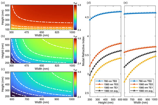
Figure 2.
Modal refractive index of the strip waveguide. (a–c) Extracted modal refractive indices of the ridge waveguide: TE0 mode at the pump wavelength (a), TE0 mode at the conversion wavelength (b), and TE1 mode at the conversion wavelength (c) for varying waveguide parameters, with white dashed lines indicating contours. (d,e) Extracted modal refractive indices as functions of the waveguide height (d) and width (e), respectively. In (d), the waveguide width is fixed at 800 nm, whereas in (e), the height is fixed at 400 nm. The modal indices are obtained using a finite-element method (FEM) solver in COMSOL Multiphysics 5.4.
The strongly confined TE0 mode at 780 nm exhibits a relatively high refractive index (denoted as ), ranging from approximately 3.8 for very shallow waveguides to around 4.6 for typical waveguide dimensions (e.g., width∼800 nm, height∼400 nm). In contrast, is lower for the 1560 nm modes, with TE0 values (denoted as ) ranging from about 2.4 (width 300 nm, height 200 nm) to 3.7 (width 800 nm, height 400 nm), and TE1 values (denoted as ) between 2.15 (width 600 nm, height 200 nm) and 3.6 (width 1000 nm, height 600 nm).
For the same waveguide height and width, the values of the three modes are compared as functions of waveguide width and height, respectively, while keeping the other parameter fixed. To satisfy the phase-matching condition, , the modal indices must strictly obey . In Figure 2d,e, is plotted in blue and in black. Clearly, no crossing occurs, indicating that the modal phase-matching condition cannot be satisfied. This is primarily because the strongly confined TE0 pump mode has a refractive index much higher than the 1560 nm modes, as evidenced by the colour differences in Figure 2a–c. Although the pump could in principle be lowered by employing higher-order modes such as TE2 or TE4, these modes considerably complicate the design, since the Gaussian input beam cannot efficiently excite them without a dedicated modal converter [28,29].
4. Quasi-Phase Matching Waveguide Design
The mismatch between the modal refractive indices, albeit geometric optimisation, necessitates the adoption of alternative approaches to achieve phase matching. One well-established technique is quasi-phase matching [5,30,31,32], which has been widely implemented in lithium niobate and KTP, where the index mismatch is compensated by periodic inversion of the nonlinear domain. Similar concepts have been applied to rhombohedrally stacked MoS2, where the sign of is reversed through rotational stacking of 3R-MoS2 layers along the vertical direction. However, this approach demands precise control of rotation angle and layer thickness, and so far has only extended the effective interaction length to the micrometre scale [26,27].
In general, the principle of quasi-phase matching can be understood from a Fourier perspective. For SPDC, the efficiency of generating photon pairs is determined by the longitudinal accumulation of the mode overlap factor , which quantifies the transverse overlap between the pump and the target signal and idler modes. The accumulated conversion amplitude along the propagation direction for a total length L is given by . When , the exponential causes partial cancellation and limits the growth. Quasi-phase matching compensates for the phase mismatch by ensuring that the effective mode overlap along z contains a periodic modulation whose Fourier component at provides constructive addition of the contributions from different positions.
In conventional domain-inverted QPM, flips between , producing a square-wave modulation with a strong Fourier peak at . More generally, literal sign inversion is not required: any longitudinal modulation of the effective mode overlap that produces Fourier weight at partially compensates the phase mismatch and allows gradual accumulation of photon pairs. In our design, the waveguide is grooved (schematic in Figure 3c)—its width is modulated with period , rather than flipping , where . This periodic grooving alters the mode overlap factor , producing a Fourier component at that compensates the phase mismatch, [Figure 3a,b].
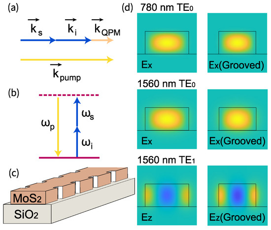
Figure 3.
The waveguide design with periodic grooving. (a) Periodic modulation of the waveguide width alters the overlap of the transverse electric fields, providing a Fourier component that compensates for the phase mismatch. (b) The energy of the conversion must still be conserved. (c) Schematic of the 3R-MoS2 thin film in a periodically grooved waveguide geometry on a SiO2 substrate. (d) Electric field distributions along the x, x, and z axes for the TE0 (780 nm), TE0 (1560 nm), and TE1 (1560 nm) modes, respectively. The mode profiles are calculated using an FDE solver in Lumerical MODE. Yellow, cyan, and blue indicate positive, zero, and negative field amplitudes, respectively.
As a starting point, we choose the dimensions of the unaltered waveguide to be 800 nm in width and 400 nm in height. These values are based on considerations of small phase mismatch and practical feasibility in fabrication. We first verify the electric field distribution within the periodically grooved waveguides, selecting a groove ratio of 15% (which affects the efficiency, as will be discussed later). The distributions of (TE0), (TE0), and (TE1) are shown for both the unaltered and grooved regions of the waveguide in Figure 3d. Despite the differences between the two, they still resemble the corresponding distributions in the strip waveguide shown in Figure 1d. This indicates that the polarisation entanglement considerations discussed previously in Section 3 remain valid.
We now examine the effect of the groove ratio and explain our considerations. Here, the groove ratio denotes the ratio of the waveguide width in the grooved region to that in the ungrooved region. The modal refractive indices are extracted for varying groove ratios, as shown in Figure 4a. Increasing the ratio reduces the waveguide width in the grooved region, effectively lowering , with the higher-order TE1 mode decreasing more rapidly than TE0. This trend is fully consistent with Figure 2e.
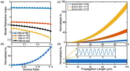
Figure 4.
Efficient down-conversion through periodic waveguide grooving. (a) Extracted modal refractive indices of the relevant optical modes in the grooved waveguide. (b) Conversion amplitude (denoted as ) after 100 m propagation for different groove ratios. For each groove ratio, the groove period is readjusted to match the corresponding phase mismatch. (c) Conversion amplitude as a function of propagation length, showing oscillatory growth for different groove ratios. The amplitudes are normalised to the oscillation amplitude of the ungrooved case. (d) Conversion amplitude in a strip waveguide without grooving, where the amplitude oscillates but does not accumulate with propagation. The inset shows a zoom-in of the short-propagation regime (0–6 m), clearly resolving the oscillations. The oscillation period is μm. For (a–d), modal indices and electric field distributions are first calculated using an FDE solver in Lumerical MODE, and the conversion amplitudes are evaluated based on the overlap of these field distributions. Losses due to Bloch scattering and material absorption are neglected because of the short propagation distance and relatively small groove ratios.
The modification of due to the introduction of grooving necessitates consideration of the local phase mismatch in each section. We therefore define an effective phase mismatch as , where and correspond to the ungrooved and grooved regions and d is the duty cycle (set to 50% in our analysis). The QPM period is then chosen such that , ensuring constructive buildup of the nonlinear signal over multiple modulation cycles.
We numerically modelled the down-conversion process in a grooved waveguide over a propagation length of 100 m. Without grooving, the conversion amplitude oscillates with a characteristic length scale given by the coherence length μm, and thus does not accumulate with increasing propagation length (Figure 4d). Introducing grooves into the waveguide adds a modulation component at the corresponding Fourier peak, effectively compensating for the phase mismatch and enabling the down-conversion amplitude to grow cumulatively.
In Figure 4c, we model the evolution of the down-conversion amplitude for different groove ratios. For each ratio, the modulation period is adjusted to match the corresponding phase mismatch , since varying the groove ratio modifies the waveguide confinement and thereby alters the modal refractive indices. The trend is clear: for groove ratios between 0% and 15%, a larger ratio enhances the modulation component at the relevant Fourier peak, leading to faster growth of the amplitude. At a groove ratio of 15%, the down-conversion amplitude is approximately 160 times larger than that without grooving, providing a clear verification of our approach. The conversion amplitude after 100 m of propagation is shown as a function of groove ratio in Figure 4b, revealing a monotonic increase up to a 0.15 groove ratio. Further increasing the groove ratio could potentially boost the conversion amplitude, but at the cost of weaker mode confinement (Figure 4a) and higher Bloch scattering losses [29].
Note that our analyses above focus on the creation of under x-polarised pump. Another Bell state, , can also be generated by employing z-polarised pump via the or tensors. A similar waveguide design, with the propagation direction oriented along the x-axis, could in principle provide a QPM condition. Nevertheless, simultaneously retaining the tunability between Bell states while achieving phase matching remains an ongoing research challenge.
5. Discussion
To summarise, we design a phase-matched approach for polarisation-entangled photon generation in integrated 3R-MoS2 waveguides. The polarisation entanglement is preserved by separating the signal and idler photons into the and components of the TE0 and TE1 modes, respectively. Phase matching is achieved through periodic modulation of the waveguide width, with a period precisely designed to compensate for the intrinsic phase mismatch. This approach provides a practical strategy to enhance the nonlinear conversion efficiency of 3R-MoS2 on an integrated platform, addressing a key limitation of 2D-material-based nonlinear photonics. Beyond this proof-of-concept, our design can be combined with advanced nanofabrication techniques and optimised waveguide engineering—such as mode-shape tailoring, dispersion engineering, or hybrid integration with low-loss photonic platforms [33,34]—to realise high-performance, low-loss on-chip entangled-photon sources. Furthermore, the flexibility and tunability of 3R-MoS2 open opportunities to extend this approach to other 2D materials or heterostructures [11,20,35], potentially covering a broad range of wavelengths and enabling multi-band or multiplexed quantum light sources. Importantly, the strategy is inherently compatible with material transfer and hetero-integration [36,37], allowing combination with mature integrated photonics platforms, single-photon detectors [38], or deterministic quantum emitters [39,40,41], further advancing scalable and versatile quantum photonic technologies.
Author Contributions
Conceptualisation, S.Y., X.L. and L.Z.; methodology, S.Y., X.L. and L.Z.; software, S.Y. and L.Z.; validation, S.Y., X.L. and L.Z.; formal analysis, S.Y., X.Z. and L.Z.; investigation, S.Y., X.Z. and L.Z.; resources, L.Z.; writing—original draft preparation, S.Y., X.L. and L.Z.; writing—review and editing, X.L. and L.Z.; visualisation, S.Y., X.Z. and L.Z.; supervision, L.Z.; project administration, L.Z.; funding acquisition, L.Z. All authors have read and agreed to the published version of the manuscript.
Funding
This work was supported by the Sichuan Science and Technology Programme under Grant Nos. 2024ZYD0050 and 2024YFHZ0369.
Data Availability Statement
The raw data that support the findings of this study are available at https://doi.org/10.5281/zenodo.17552810 and from the corresponding author upon reasonable request.
Acknowledgments
We thank Qing Zhang and Yuqi Wang for their valuable discussions.
Conflicts of Interest
The authors declare that they have no competing interests.
References
- Thomas, P.; Ruscio, L.; Morin, O.; Rempe, G. Fusion of deterministically generated photonic graph states. Nature 2024, 629, 567–572. [Google Scholar] [CrossRef]
- Yu, S.; Zhang, X.; Lei, X.; Zhai, L. A Concise Primer on Solid-State Quantum Emitters. IEEE J. Sel. Top. Quantum Electron. 2025, 31, 6700616. [Google Scholar] [CrossRef]
- Liu, S.; Wang, Y.; Saleem, Y.; Li, X.; Liu, H.; Yang, C.A.; Yang, J.; Ni, H.; Niu, Z.; Meng, Y.; et al. Quantum correlations of spontaneous two-photon emission from a quantum dot. Nature 2025, 643, 1234–1239. [Google Scholar] [CrossRef]
- Laneve, A.; Rota, M.B.; Basso Basset, F.; Beccaceci, M.; Villari, V.; Oberleitner, T.; Reum, Y.; Krieger, T.M.; Buchinger, Q.; Prasad, R.; et al. Wavevector-resolved polarization entanglement from radiative cascades. Nat. Commun. 2025, 16, 6209. [Google Scholar] [CrossRef] [PubMed]
- Lin, J.; Yao, N.; Hao, Z.; Zhang, J.; Mao, W.; Wang, M.; Chu, W.; Wu, R.; Fang, Z.; Qiao, L.; et al. Broadband quasi-phase-matched harmonic generation in an on-chip monocrystalline lithium niobate microdisk resonator. Phys. Rev. Lett. 2019, 122, 173903. [Google Scholar] [CrossRef] [PubMed]
- Larsen, M.V.; Collins, M.J.; Broome, M.A.; Strain, M.J.; Tame, M.S.; Almeida, M.P.; Reid, M.D.; White, A.G. Deterministic generation of a two-dimensional cluster state. Science 2019, 365, 369–372. [Google Scholar] [CrossRef] [PubMed]
- Lu, C.Y.; Yang, T.; Pan, J.W. Experimental Multiparticle Entanglement Swapping for Quantum Networking. Phys. Rev. Lett. 2009, 103, 020501. [Google Scholar] [CrossRef]
- Villar, A.; Lohrmann, A.; Ling, A. Experimental entangled photon pair generation using crystals with parallel optical axes. Opt. Express 2018, 26, 12396. [Google Scholar] [CrossRef]
- Elshaari, A.W.; Pernice, W.; Srinivasan, K.; Benson, O.; Zwiller, V. Hybrid integrated quantum photonic circuits. Nat. Photonics 2020, 14, 285–298. [Google Scholar] [CrossRef]
- Zhou, X.; Zhai, L.; Liu, J. Epitaxial quantum dots: A semiconductor launchpad for photonic quantum technologies. Photonics Insights 2023, 1, R07. [Google Scholar] [CrossRef]
- Autere, A.; Jussila, H.; Dai, Y.; Wang, Y.; Lipsanen, H.; Sun, Z. Nonlinear optics with two-dimensional layered materials. Adv. Mater. 2018, 30, 1705963. [Google Scholar] [CrossRef]
- Xu, X.; Trovatello, C.; Mooshammer, F.; Shao, Y.; Zhang, S.; Yao, K.; Basov, D.N.; Cerullo, G.; Schuck, P.J. Towards compact phase-matched and waveguided nonlinear optics in atomically layered semiconductors. Nat. Photonics 2022, 16, 698–706. [Google Scholar] [CrossRef]
- Tang, J.; Gao, M.; Zhang, Q.; Yang, Y. Giant second-harmonic generation in rhombohedral transition metal dichalcogenide metasurfaces. Opt. Commun. 2025, 584, 131825. [Google Scholar] [CrossRef]
- Xu, D.; Peng, Z.H.; Trovatello, C.; Cheng, S.W.; Xu, X.; Sternbach, A.; Basov, D.N.; Schuck, P.J.; Delor, M. Spatiotemporal imaging of nonlinear optics in van der Waals waveguides. Nat. Nanotechnol. 2025, 20, 374–380. [Google Scholar] [CrossRef] [PubMed]
- Tang, Y.; Qin, H.; de Ceglia, D.; Yang, W.; Shameli, M.A.; Nauman, M.; Morales, R.C.; Yan, J.; Wang, C.; Qiu, S.; et al. Giant Second Harmonic Generation from 3R-MoS2 Metasurfaces. arXiv 2025, arXiv:2503.20161. [Google Scholar]
- Trolle, M.L.; Tsao, Y.C.; Pedersen, K.; Pedersen, T.G. Observation of excitonic resonances in the second harmonic spectrum of MoS2. Phys. Rev. B 2015, 92, 161409. [Google Scholar] [CrossRef]
- Zograf, G.; Küçüköz, B.; Polyakov, A.Y.; Yankovich, A.B.; Ranjan, A.; Bancerek, M.; Agrawal, A.V.; Olsson, E.; Wieczorek, W.; Antosiewicz, T.J.; et al. Ultrathin 3R-MoS2 metasurfaces with atomically precise edges for efficient nonlinear nanophotonics. Commun. Phys. 2025, 8, 271. [Google Scholar] [CrossRef]
- Seidt, L.; Weber, T.; Seredin, A.A.; Possmayer, T.; Savelev, R.; Petrov, M.I.; Maier, S.A.; Tittl, A.; de S. Menezes, L.; Sortino, L. Ultrafast all-optical switching in nonlinear 3R-MoS2 van der Waals metasurfaces. npj Nanophotonics 2025, 2, 37. [Google Scholar] [CrossRef]
- Qin, B.; Ma, C.; Guo, Q.; Li, X.; Wei, W.; Ma, C.; Wang, Q.; Liu, F.; Zhao, M.; Xue, G.; et al. Interfacial epitaxy of multilayer rhombohedral transition-metal dichalcogenide single crystals. Science 2024, 385, 99–104. [Google Scholar] [CrossRef]
- Wang, L.; Qi, J.; Wei, W.; Wu, M.; Zhang, Z.; Li, X.; Sun, H.; Guo, Q.; Cao, M.; Wang, Q.; et al. Bevel-edge epitaxy of ferroelectric rhombohedral boron nitride single crystal. Nature 2024, 629, 74–79. [Google Scholar] [CrossRef]
- Liu, L.; Li, T.; Gong, X.; Wen, H.; Zhou, L.; Feng, M.; Zhang, H.; Zou, N.; Wu, S.; Li, Y.; et al. Homoepitaxial growth of large-area rhombohedral-stacked MoS2. Nat. Mater. 2025, 24, 1195–1202. [Google Scholar] [CrossRef]
- Weissflog, M.A.; Fedotova, A.; Tang, Y.; Santos, E.A.; Laudert, B.; Shinde, S.; Abtahi, F.; Afsharnia, M.; Pérez Pérez, I.; Ritter, S.; et al. A tunable transition metal dichalcogenide entangled photon-pair source. Nat. Commun. 2024, 15, 7600. [Google Scholar] [CrossRef]
- Feng, J.; Wu, Y.; Duan, R.; Wang, J.; Chen, W.; Qin, J.; Liu, Z.; Guo, G.C.; Ren, X.F.; Qiu, C.W. Polarization-entangled photon-pair source with van der Waals 3R-WS2 crystal. eLight 2024, 4, 16. [Google Scholar] [CrossRef]
- Lyu, X.; Kallioniemi, L.; Hong, H.; Qu, R.; Zhang, Y.; Zúñiga-Perez, J.; Liu, K.; Gao, W. A tunable entangled photon-pair source based on a Van der Waals insulator. Nat. Commun. 2025, 16, 1899. [Google Scholar] [CrossRef] [PubMed]
- Hong, H.; Huang, C.; Ma, C.; Qi, J.; Shi, X.; Liu, C.; Wu, S.; Sun, Z.; Wang, E.; Liu, K. Twist-phase-matching in two-dimensional materials. Phys. Rev. Lett. 2023, 131, 233801. [Google Scholar] [CrossRef] [PubMed]
- Tang, Y.; Sripathy, K.; Qin, H.; Lu, Z.; Guccione, G.; Janousek, J.; Zhu, Y.; Hasan, M.M.; Iwasa, Y.; Lam, P.K.; et al. Quasi-phase-matching enabled by van der Waals stacking. Nat. Commun. 2024, 15, 9979. [Google Scholar] [CrossRef]
- Trovatello, C.; Ferrante, C.; Yang, B.; Bajo, J.; Braun, B.; Peng, Z.H.; Xu, X.; Jenke, P.K.; Ye, A.; Delor, M.; et al. Quasi-phase-matched up- and down-conversion in periodically poled layered semiconductors. Nat. Photonics 2025, 19, 291–299. [Google Scholar] [CrossRef]
- Dai, D.; Tang, Y.; Bowers, J.E. Mode conversion in tapered submicron silicon ridge optical waveguides. Opt. Express 2012, 20, 13425–13439. [Google Scholar] [CrossRef]
- Liu, J.; Duan, J.; Zhu, P.; Xia, G.; Hong, Q.; Zhang, K.; Zhu, Z.; Qin, S.; Xu, P. Modal phase-matching in thin-film lithium niobate waveguides for efficient generation of entangled photon pairs. Opt. Express 2024, 32, 40629–40639. [Google Scholar] [CrossRef]
- Wang, C.; Xiong, X.; Andrade, N.; Venkataraman, V.; Ren, X.F.; Guo, G.C.; Lončar, M. Second harmonic generation in nano-structured thin-film lithium niobate waveguides. Opt. Express 2017, 25, 6963–6973. [Google Scholar] [CrossRef]
- Imbrock, J.; Wesemann, L.; Kroesen, S.; Ayoub, M.; Denz, C. Waveguide-integrated three-dimensional quasi-phase-matching structures. Optica 2020, 7, 28–34. [Google Scholar] [CrossRef]
- Nitiss, E.; Hu, J.; Stroganov, A.; Brès, C.S. Optically reconfigurable quasi-phase-matching in silicon nitride microresonators. Nat. Photonics 2022, 16, 134–141. [Google Scholar] [CrossRef]
- Wang, J.F.; Yan, F.F.; Li, Q.; Liu, Z.H.; Liu, H.; Guo, G.P.; Guo, L.P.; Zhou, X.; Cui, J.M.; Wang, J.; et al. Coherent Control of Nitrogen-Vacancy Center Spins in Silicon Carbide at Room Temperature. Phys. Rev. Lett. 2020, 124, 223601. [Google Scholar] [CrossRef] [PubMed]
- PsiQuantum Team. A manufacturable platform for photonic quantum computing. Nature 2025, 641, 876–883. [Google Scholar] [CrossRef]
- Guo, Q.; Qi, X.Z.; Zhang, L.; Gao, M.; Hu, S.; Zhou, W.; Zang, W.; Zhao, X.; Wang, J.; Yan, B.; et al. Ultrathin quantum light source with van der Waals NbOCl2 crystal. Nature 2023, 613, 53–59. [Google Scholar] [CrossRef]
- Pelgrin, V.; Yoon, H.; Cassan, E.; Sun, Z. Hybrid integration of 2D materials for on-chip nonlinear photonics. Light Adv. Manuf. 2023, 4, 311–333. [Google Scholar] [CrossRef]
- Azimi, A.; Barrier, J.; Barreda, A.; Bauer, T.; Bouzari, F.; Brokkelkamp, A.; de Mongeot, F.B.; Parsons, T.; Christianen, P.; Conesa-Boj, S.; et al. Photonics in Flatland: Challenges and Opportunities for Nanophotonics with 2D Semiconductors. arXiv 2025, arXiv:2507.00336. [Google Scholar] [CrossRef]
- Gyger, S.; Zichi, J.; Schweickert, L.; Elshaari, A.W.; Steinhauer, S.; Covre da Silva, S.F.; Rastelli, A.; Zwiller, V.; Jöns, K.D.; Errando-Herranz, C. Reconfigurable photonics with on-chip single-photon detectors. Nat. Commun. 2021, 12, 1408. [Google Scholar] [CrossRef]
- Zhai, L.; Löbl, M.C.; Jahn, J.P.; Huo, Y.; Treutlein, P.; Schmidt, O.G.; Rastelli, A.; Warburton, R.J. Large-range frequency tuning of a narrow-linewidth quantum emitter. Appl. Phys. Lett. 2020, 117, 083106. [Google Scholar] [CrossRef]
- Uppu, R.; Midolo, L.; Zhou, X.; Carolan, J.; Lodahl, P. Quantum-dot-based deterministic photon–emitter interfaces for scalable photonic quantum technology. Nat. Nanotechnol. 2021, 16, 1308–1317. [Google Scholar] [CrossRef]
- Spinnler, C.; Nguyen, G.N.; Wang, Y.; Zhai, L.; Javadi, A.; Erbe, M.; Scholz, S.; Wieck, A.D.; Ludwig, A.; Lodahl, P.; et al. A single-photon emitter coupled to a phononic-crystal resonator in the resolved-sideband regime. Nat. Commun. 2024, 15, 9509. [Google Scholar] [CrossRef]
Disclaimer/Publisher’s Note: The statements, opinions and data contained in all publications are solely those of the individual author(s) and contributor(s) and not of MDPI and/or the editor(s). MDPI and/or the editor(s) disclaim responsibility for any injury to people or property resulting from any ideas, methods, instructions or products referred to in the content. |
© 2025 by the authors. Licensee MDPI, Basel, Switzerland. This article is an open access article distributed under the terms and conditions of the Creative Commons Attribution (CC BY) license (https://creativecommons.org/licenses/by/4.0/).