1. Introduction
Metamaterial absorbers (MAs) have attracted significant attention in recent years due to their promising applications in stealth technology, sensing, and multispectral thermal detection [
1,
2]. Microwave absorbers with wideband tunable absorption are of great importance for a wide range of practical applications in both military and daily life. For instance, MAs can be used to reduce radar cross-section (RCS) and electromagnetic interference (EMI) [
3,
4,
5,
6]. Nowadays, several absorbers in the microwave and optical regimes have been developed utilizing the special characteristics of metamaterials [
7,
8]. In certain applications, such as aircraft cockpit windows, optical detectors, and aerospace equipment, an optically transparent and flexible absorber is highly desirable.
Metasurfaces [
9], regarded as the two-dimensional equivalents of metamaterials, are composed of multiple subwavelength components periodically placed on a planar surface. In comparison to three-dimensional metamaterials, metasurfaces are ultrathin and lightweight and have a relatively simple structure. They have been extensively used in various electromagnetic (EM) applications such as polarization conversion, wideband EM wave absorption, and RCS reduction [
10,
11,
12].
Graphene, a one-atom-thick sheet of carbon atoms arranged in a honeycomb lattice, has unique properties. It offers exceptional mechanical strength, robust thermal stability, and excellent electrical conductivity. Due to the low density of states near the Dirac point, its Fermi level can be tuned with a bias voltage, allowing control of electromagnetic waves across a broad spectral range. These distinctive features, along with its adjustable electromagnetic response, have made graphene a strong candidate for tunable absorbers with high optical transparency [
13]. Graphene’s tunable conductivity enables dynamic control of the absorption bands, while metallic and dielectric metamaterials can achieve only non-dynamic control of their absorption bands through fine-tuning their geometrical parameters. Moreover, multi-band perfect absorption can be achieved by using single-layer graphene gratings due to the excitation of standing-wave graphene surface plasmon polaritons [
14,
15].
Graphene-based metasurfaces are being suggested for designing microwave absorbers with tunable absorption and RCS reduction, while also allowing for transparency and flexibility [
16,
17]. For example, integrating a graphene sandwich structure can facilitate adaptive microwave absorption through electrostatic doping of conductivity; Balci [
18] proposed a reconfigurable graphene-based absorber with this approach. In [
19], a transparent tunable absorber is created by patterning graphene into discrete patches, using two techniques: the ‘surface resistance approach’ and the ‘stacking graphene metasurface’ approach. Lu et al. [
20] combined a graphene metasurface with an oxide–metal-oxide ground plane to produce a wideband microwave absorber with high transparency and sufficient flexibility. In [
21], a transparent, tunable microwave absorber was created using a combination of patterned graphene and indium tin oxide (ITO). Wang et al. [
22] developed a dual-tunable microwave absorber using a graphene metasurface, in which applying separate bias voltages to either continuous or patterned graphene enables independent control of the absorption frequency and amplitude. Geng et al. [
23] created an effective microwave absorber based on graphene that can change its center frequency within the Ku band. However, this design is not optically transparent because the patterned graphene is directly deposited onto a layer of periodic metal patches.
In this work, we present the design of an optically transparent and flexible microwave tunable absorber, covering both the X and Ku frequency bands. The absorber is based on a metasurface composed of a periodic array of graphene spiral resonators (GSRs) attached to an ultrathin polyethylene terephthalate (PET) film, which is placed over an ITO-backed dielectric spacer. An equivalent circuit model (ECM) described by closed-form equations is proposed to help optimize the structure to achieve maximum absorption within the targeted frequency range. The incident angle insensitivity of the absorber for both TE and TM wave polarizations is also investigated. In addition, to broaden the absorber’s bandwidth, a double-layer graphene spiral resonator (DGSR) metasurface is designed, and its absorption performance is evaluated.
2. Absorber Design and Equivalent Circuit Model
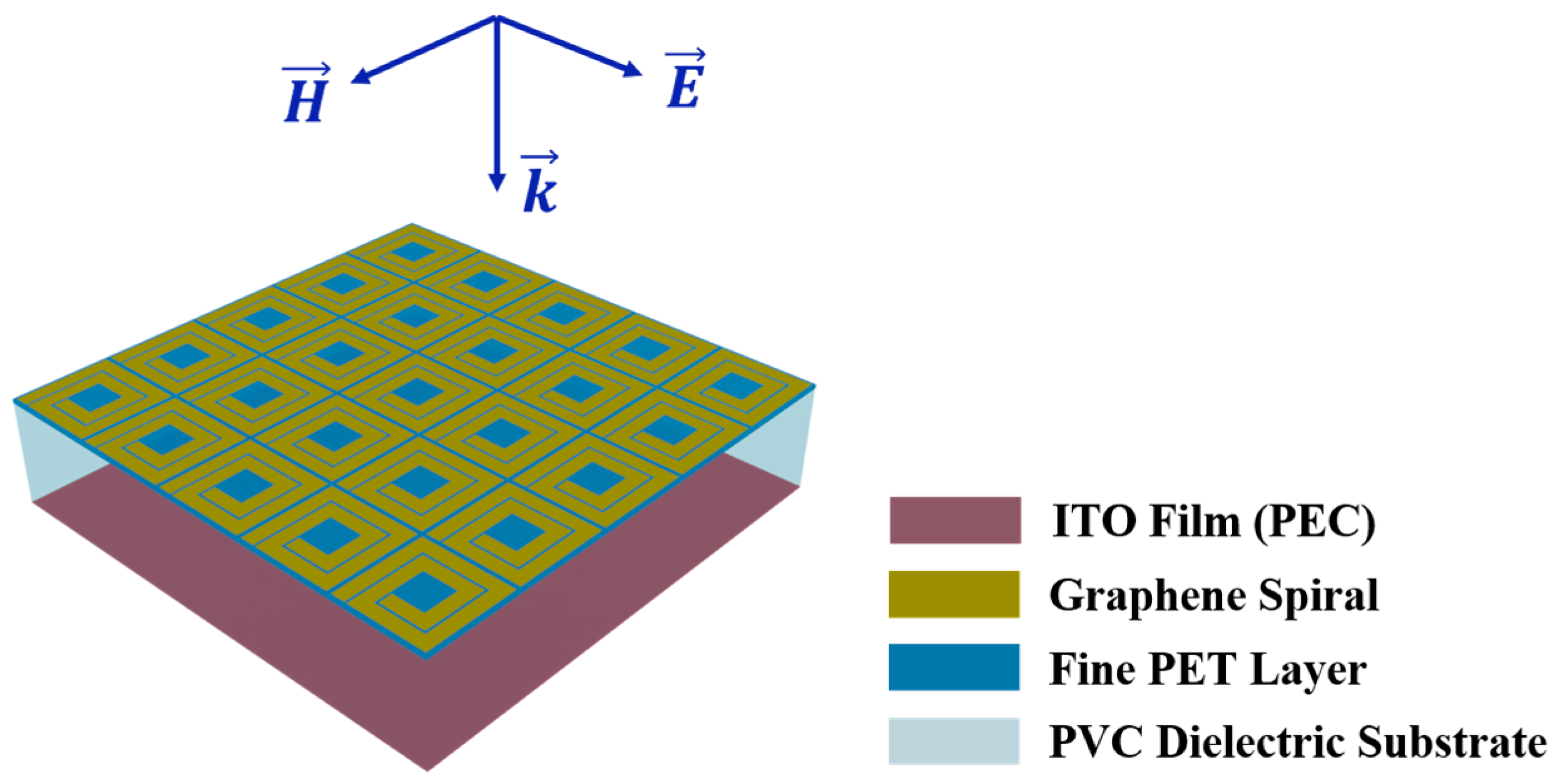
A perspective view of the proposed MA’s schematic is illustrated in
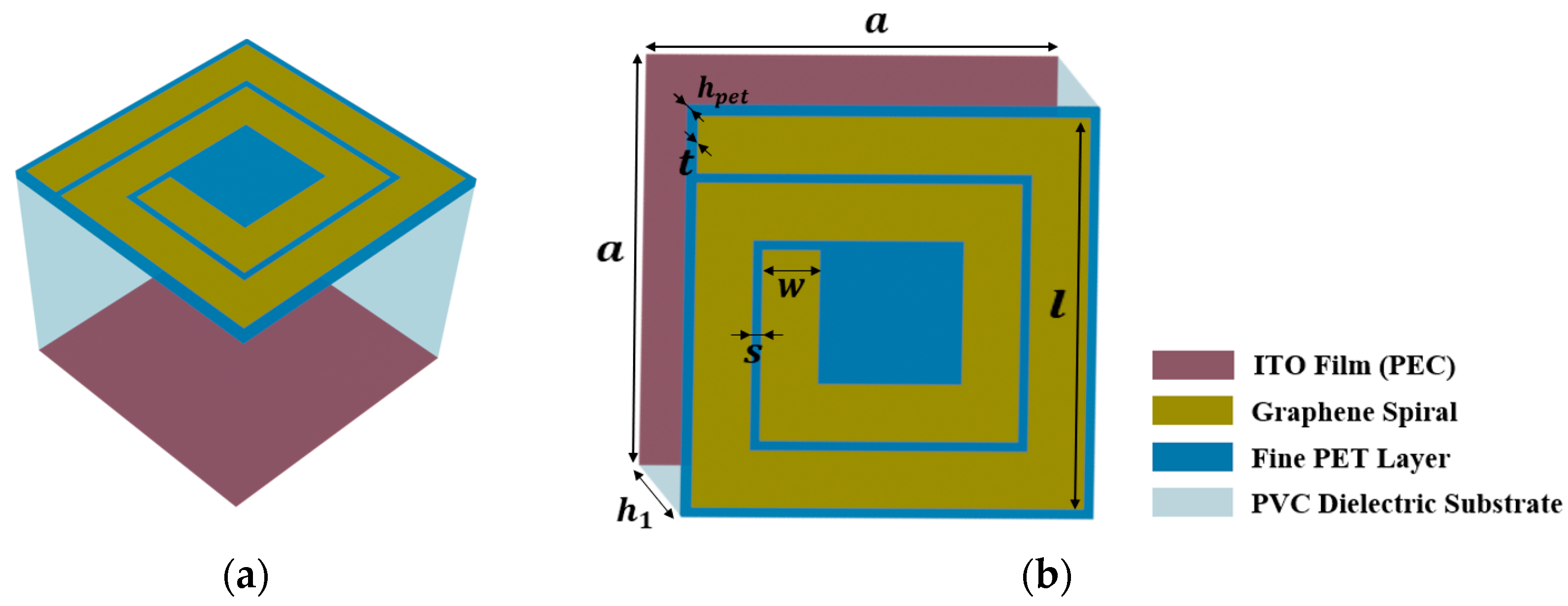
Figure 1, while its unit cell, which consists of three stacking functional layers, is depicted in
Figure 2. The upper layer consists of a square graphene spiral resonator (GSR) attached to a 0.125 mm thick PET film. Square spiral resonators have been extensively used as metamaterial unit cells to offer a high level of miniaturization [
24,
25]. PET was chosen because of its optical transparency and mechanical flexibility. Moreover, monolayer graphene attached to PET film is nowadays commercially available [
26]. The middle layer (spacer) is a transparent, flexible dielectric layer (PVC) with a thickness equal to one-quarter wavelength in the medium. The bottom surface of the dielectric spacer is backed by an indium tin oxide (ITO) ultrathin layer, which has a low sheet resistance (~6 Ω/sq) and acts as a reflective ground plane (PEC), providing zero transmission. The use of a low-sheet-resistance ITO layer instead of a metal plane has the advantages of high optical transparency and flexibility. The relative dielectric constants of PET and PVC are taken to be
and
, respectively. In the microwave regime, the loss tangents of PET and PVC films are
= 0.02 and
= 0.00033, respectively [
27]. The geometric parameters of the square GSR are as follows: the number of turns
N of the spiral, the side length of the external turn
, the width of the strips
w, and the separation between two adjacent turns
s. The unit cell size of the MA and the PVC-substrate thickness are denoted by
a = l + 2
s and
respectively. It should be noticed that the maximum number of spiral turns should satisfy the structure’s filling factor restriction:
.
It is well known that the dimensions of the structural components of the unit cell significantly affect the maximum absorption and the corresponding operating frequency range. To optimize the structure for maximum absorption across a broad frequency range, we developed an ECM using analytical expressions for resistive, capacitive, and inductive elements. Equivalent circuit models have been successfully utilized to design MAs [
28,
29]. They are useful tools that provide accurate results and yield valuable physical insights into the absorption characteristics of the structure and the impact that different parameters have.
In our ECM, the GSR is represented by the series combination of a resistor
, an inductor
and a capacitor
with a shunt resistance
that takes into account the dissipation in the lossy PET thin substrate. Following Ref. [
30], the equivalent impedance of the GSR is given by
where
with
where
) is the complete elliptic integral of the first kind and
.
The above closed-form equations have been validated in previous studies of metallic metamaterials based on the spiral geometry [
25,
31].
Based on Kubo’s formula [
32], there are two primary factors contributing to the surface conductivity of graphene: intraband and interband electronic transitions. In the microwave regime, interband transitions are extremely weak. In contrast, the contribution due to intraband transitions is the dominant one. Thus, considering
as the time harmonic dependency, the surface conductivity of the monolayer graphene can be expressed as [
32]
where ω is the angular frequency;
is the Fermi energy;
Γ is the electron scattering rate that is assumed to be energy independent;
T is the temperature;
e is the electron charge;
is the reduced Planck constant; and
is the Boltzmann constant.
Γ = 1/(2τ), where
τ is the electron–phonon relaxation time. In this work,
τ = 0.2
ps is used, which is consistent with measurements for monolayer graphene produced by chemical vapor deposition (CVD) [
19], and the ambient temperature (
T = 300 K) is assumed. Although the relaxation time depends on both the Fermi energy and the frequency [
33], such dependencies are typically weak; thus, we do not expect them to influence our main conclusions.
In the ECM, the PVC grounded substrate (spacer) can be modeled as a short-circuited transmission line because the ITO ground plane acts as a PEC. The impedance of the PVC spacer is given by
where
is the characteristic impedance of the PVC spacer for transverse electric (TE) or transverse magnetic (TM) polarized waves;
is the propagation constant,
with
is the thickness of the PVC spacer; and
denotes the incidence angle of the obliquely incoming waves into the structure. Moreover, the following equations give the characteristic impedances for TM- and TE-polarized waves:
It is obvious from Equations (8) and (9) that the characteristic impedance of the PVC spacer is a function of the incident angle for both polarizations. It should be noticed that the equivalent capacitance of the GSR metasurface should be modified for the case of oblique incidence as follows [
34,
35]:
Furthermore, the sheet impedance of graphene remains almost constant with the incident angle and polarization state due to the negligible spatial dispersion of graphene.
We utilize the ECM depicted in
Figure 3 to optimize the proposed absorber for high absorption across a broad frequency range, covering both X and Ku bands. The absorbance of an MA can be expressed in terms of S-scattering parameters as
Since the ITO ground plane results in almost vanishing transmission
, Equation (11) for normal incidence can be written as
The input impedance of the absorber
can be calculated by
where
is given by Equation (8), and
is the free space wave impedance. In the case of oblique incidence, the wave impedances in free space should be modified for both TE and TM wave polarizations as follows [
34,
35]:
and the scattering parameter
in Equation (12) should be replaced by
for TE and TM wave polarizations, respectively.
In the following, using the analytical expressions of our ECM, we can identify optimized geometrical and electrical parameters of the structure for achieving wideband high absorption (>90%) covering both the X (8–12 GHz) and Ku (12–18 GHz) bands. At first, the thickness of the PVC dielectric spacer is selected to be equal to one-quarter wavelength according to interference cancellation theory [
36]:
where
is taken to be the central frequency of the desired operating frequency band. Hence, from Equation (16), we obtain
. After investigating the dependence of the resonant frequency
on the GSR’s number of turns
and its geometric parameters, a set of initial parameters can be selected:
The thickness of the graphene spirals is taken to be
. According to Equation (12), perfect absorption could be achieved when the impedance matching condition
is satisfied; i.e., the real and imaginary parts of the input impedance should be
and
, respectively, for a wideband frequency range. The optimized values of the geometric parameters can be easily found with the aid of a simple optimization algorithm with the cost function defined by the above impedance matching condition. Finally, the optimum values of the structural parameters of the proposed absorber are found to be
.
3. Absorber Performance and Parameter Retrieval Method
In this section, we demonstrate the performance of the designed MA by considering a plane EM wave in the microwave regime impinging on the GSR metasurface. Initially, we assume normal incidence of an EM wave with transverse electric (TE) or transverse magnetic (TM) polarization.
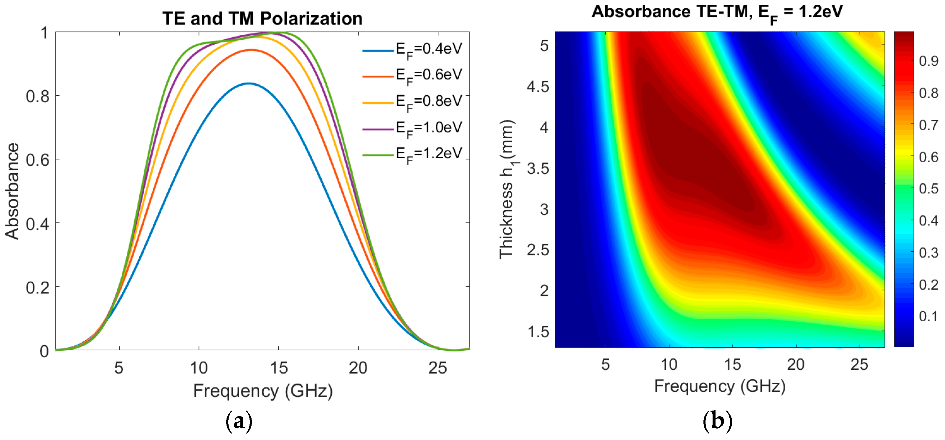
Figure 4a depicts the tunability of the absorption spectra by adjusting the Fermi energy of graphene from 0.4 eV to 1.2 eV. Note that, based on experimental evidence, the Fermi energy of graphene can be effectively modulated from 0.4 to 1.2 eV by adjusting a DC voltage [
37]. The DC bias voltage can be applied directly between the patterned graphene metasurface and the ITO ground plane. However, a more efficient application scheme of the DC bias voltage is the utilization of an ionic liquid electrolyte (or gel). In this scheme, an ultrathin layer of ionic gel can be coated on the graphene as a high-capacitance spacer layer between a top metal electrode and the patterned graphene, as described in Refs. [
19,
21]. The ionic gel generates high carrier densities in graphene, causing an increase in the Fermi energy. It is worth noting that, with the aid of ionic liquids, a significant range of Fermi energies can be obtained by applying a moderate DC voltage [
18].
As shown in
Figure 4a, both the maximum absorbance and the bandwidth increase as the Fermi energy
is increased, and for
the MA demonstrates more than 90% absorbance with a bandwidth of 8.9 GHz, covering both the X and Ku bands. To characterize the absorption performance for the MA, we can calculate the relative absorption bandwidth (RBW) defined as
where
and
are the upper and lower frequencies corresponding to the absorption frequency range with absorbance more than 90%. The proposed MA achieves an
of 68%, and thus, ultrawideband is achieved, which is a demanding feature for modern microwave applications. Moreover, the MA shows a peak absorbance of 99.7% at
.
The thickness of the PVC spacer is a crucial geometrical parameter determining the absorption spectrum due to impedance mismatch. In our design, the thickness is chosen to be one-quarter wavelength in the medium, i.e.,
. By varying the thickness
, while keeping other parameters unchanged, the absorption spectrum is significantly affected, as shown in
Figure 4b. When the PVC thickness is
the absorber performs effectively in the frequency band between 8.5 GHz and 17.35 GHz. If the PVC thickness is smaller than
the absorption band is shifted to a higher frequency range, whereas if the PVC thickness is larger than
, the absorption band is shifted to a lower frequency range.
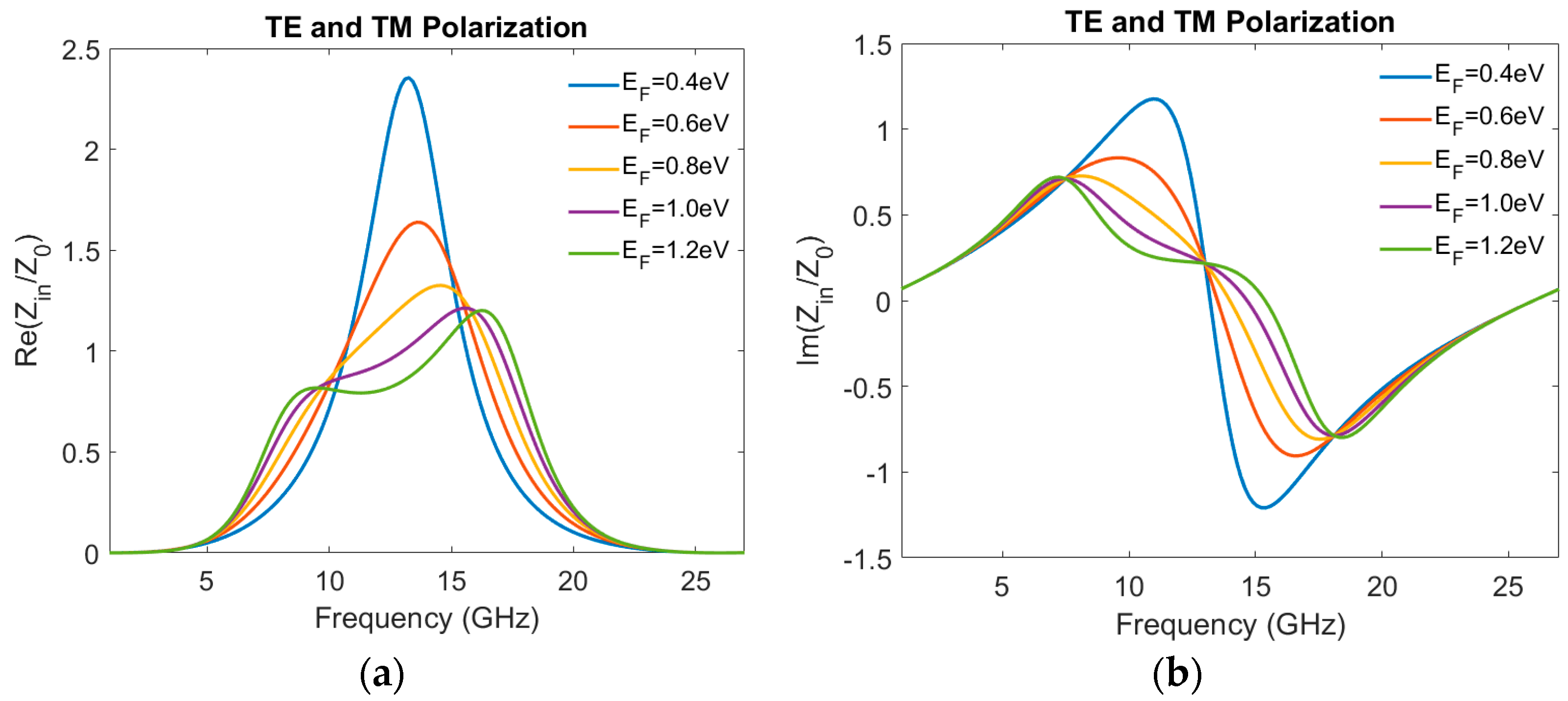
To gain a deeper insight into the tuning mechanism of absorbance amplitude, the real and imaginary parts of the normalized input impedance,
, at different Fermi energies, are illustrated in
Figure 5a,b, respectively. It can be seen that, as the graphene Fermi energy increases, the real part of impedance fluctuates around 1 while the imaginary part fluctuates around 0 across the desired frequency range. This suppresses the reflection of the incident waves by the absorber, resulting in enhanced absorption. Thus, by changing the graphene conductivity
the absorption amplitude can be tuned in accordance with the input impedance matching, enabling efficient wideband absorption.
It is well known that the response of EM metamaterials can be characterized using equivalent EM parameters, such as effective permittivity
and effective permeability
. These effective constitutive parameters can also serve as a significant tool for validating the absorbing mechanism [
38]. The Nicolson–Ross–Weir (NRW) retrieval method [
39,
40] provides a feasible method for extracting these parameters. According to the NRW technique, the effective permittivity and effective permeability of the proposed MA can be evaluated through the use of the S-parameters as follows [
40]:
where
is the thickness of the absorber, and
denotes the propagation constant in free space. Since
due to the ITO ground plane (PEC), Equation (17) can be simplified as
where
can be calculated analytically from the input impedance of the structure under normal incidence.
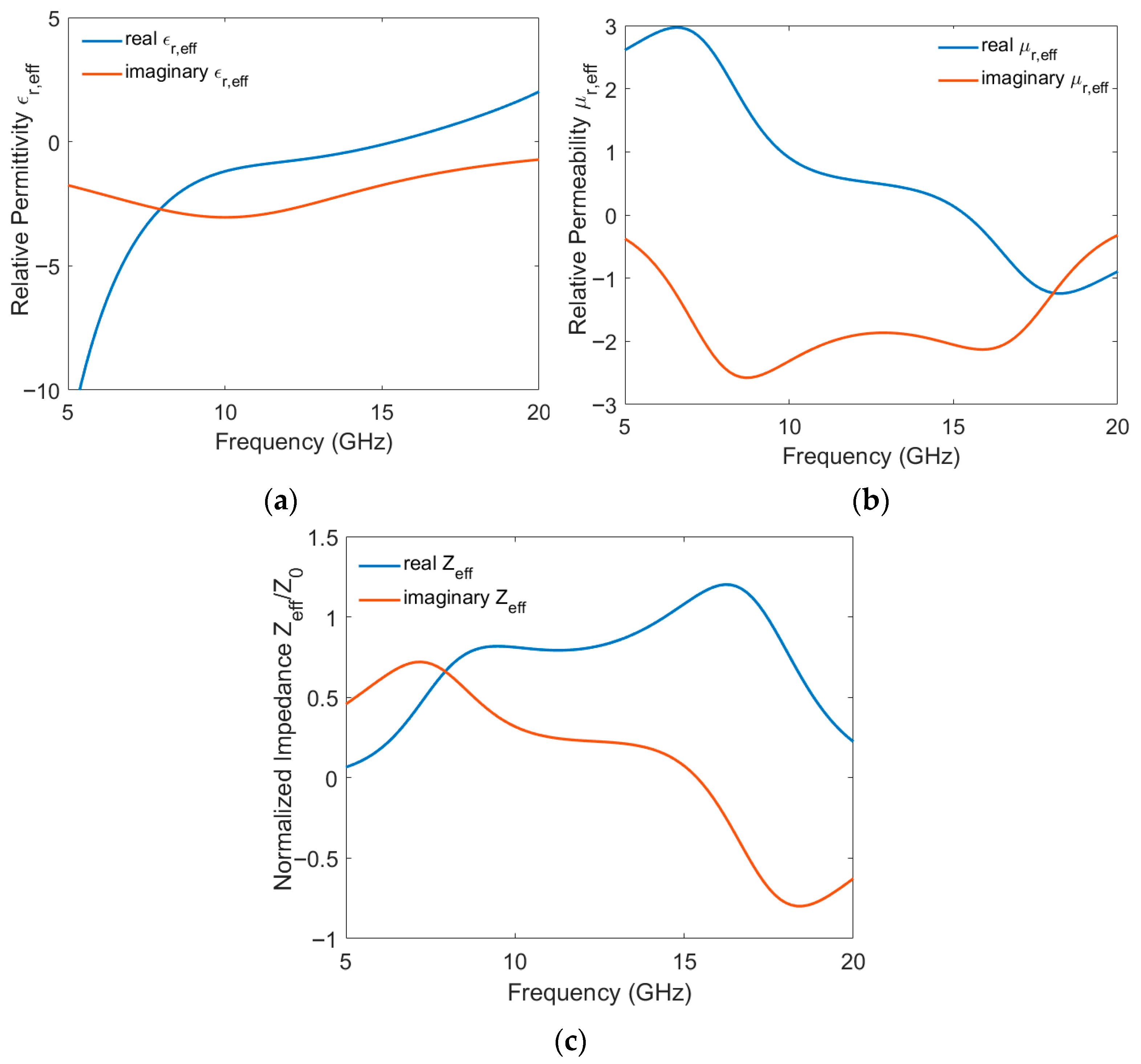
Figure 6a,b show the effective permittivity
and the effective permeability
of the proposed absorber as a function of frequency. It can be seen that, in the frequency range of interest (X and Ku bands), the structure exhibits a single-negative (SNG) metamaterial property characterized by a negative value of either the real permittivity or the real permeability [
41]. The imaginary parts of the permittivity and permeability account for the losses and represent the material’s impact on absorbing the incident electromagnetic waves. Using the extracted electromagnetic parameters
and
, the normalized effective impedance as a function of frequency can be calculated as [
39]
Figure 6c presents the frequency dependence of both the real and imaginary parts of the normalized effective impedance
which is derived from the obtained effective parameters. These curves coincide with the corresponding ones for the real and imaginary parts of the input impedance of the absorber obtained by the ECM at the Fermi energy
Consequently, the results of the effective parameter retrieval method support the reliability of our ECM.
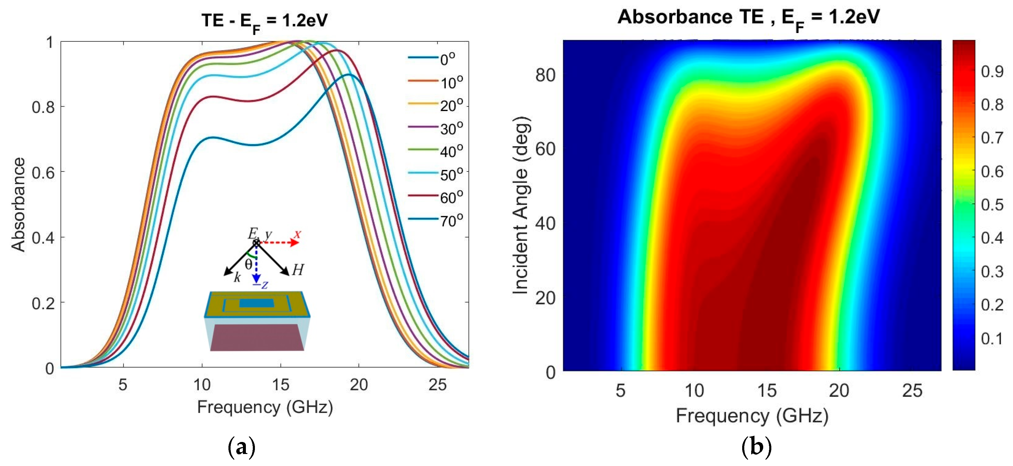
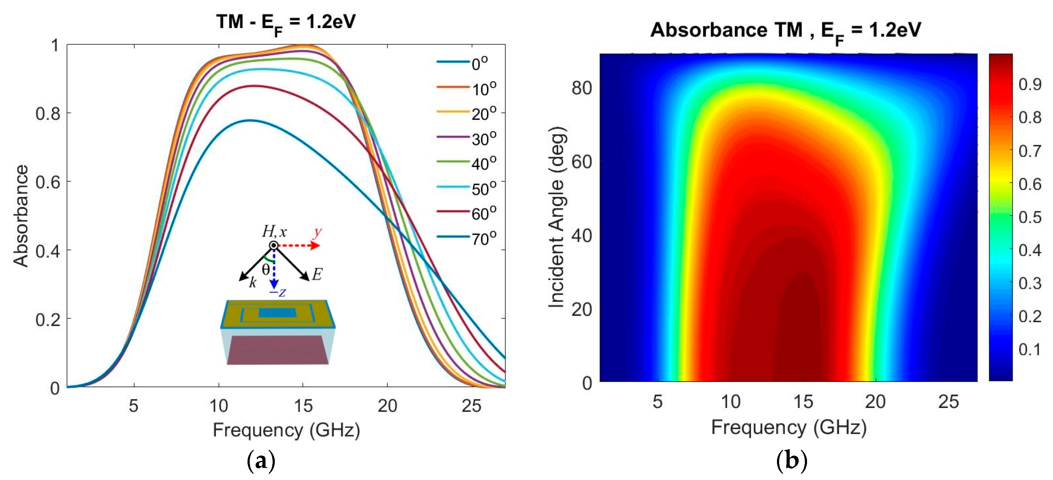
Next, the absorbance of the designed MA under oblique incidence is considered. To investigate the angular stability of the absorber, the absorbance is calculated as a function of frequency and incident angle for both TE and TM wave polarizations.
Figure 7a illustrates the absorption spectrum at different incident angles from 0° to 70° for an EM wave with TE polarization, while
Figure 7b presents the contour map of the absorbance spectrum as a function of the incident angle. The corresponding plots for an EM wave with TM polarization are presented in
Figure 8a,b, respectively.
With the increase in the incident angle, the absorbance gradually decreases. This reduction observed at greater incident angles is anticipated due to increased reflection and less interaction between the incoming waves and the metasurface at steeper angles. The absorption performance under TM incidence is inferior to that under TE incidence for the same incident angle. Interestingly, in TE polarization, the absorption bandwidth is increased, and the absorbance peak is blue-shifted as the incident angle increases. On the contrary, the absorption bandwidth of TM polarization is slightly narrowed as the angle of incidence increases. The proposed absorber maintains a high absorbance of above 90% at an incident angle up to 50° for both TE and TM polarizations. Moreover, the structure guarantees an absorbance of more than 80% for both TE and TM polarizations, when the incident angle is increased to 60°. Notably, this wide-angle stability covers the target frequency bands (X-Ku) with an RBW of about 68% for TE waves and of about 60% for TM waves.
4. Design of a Double-Layer GSR Metasurface Absorber
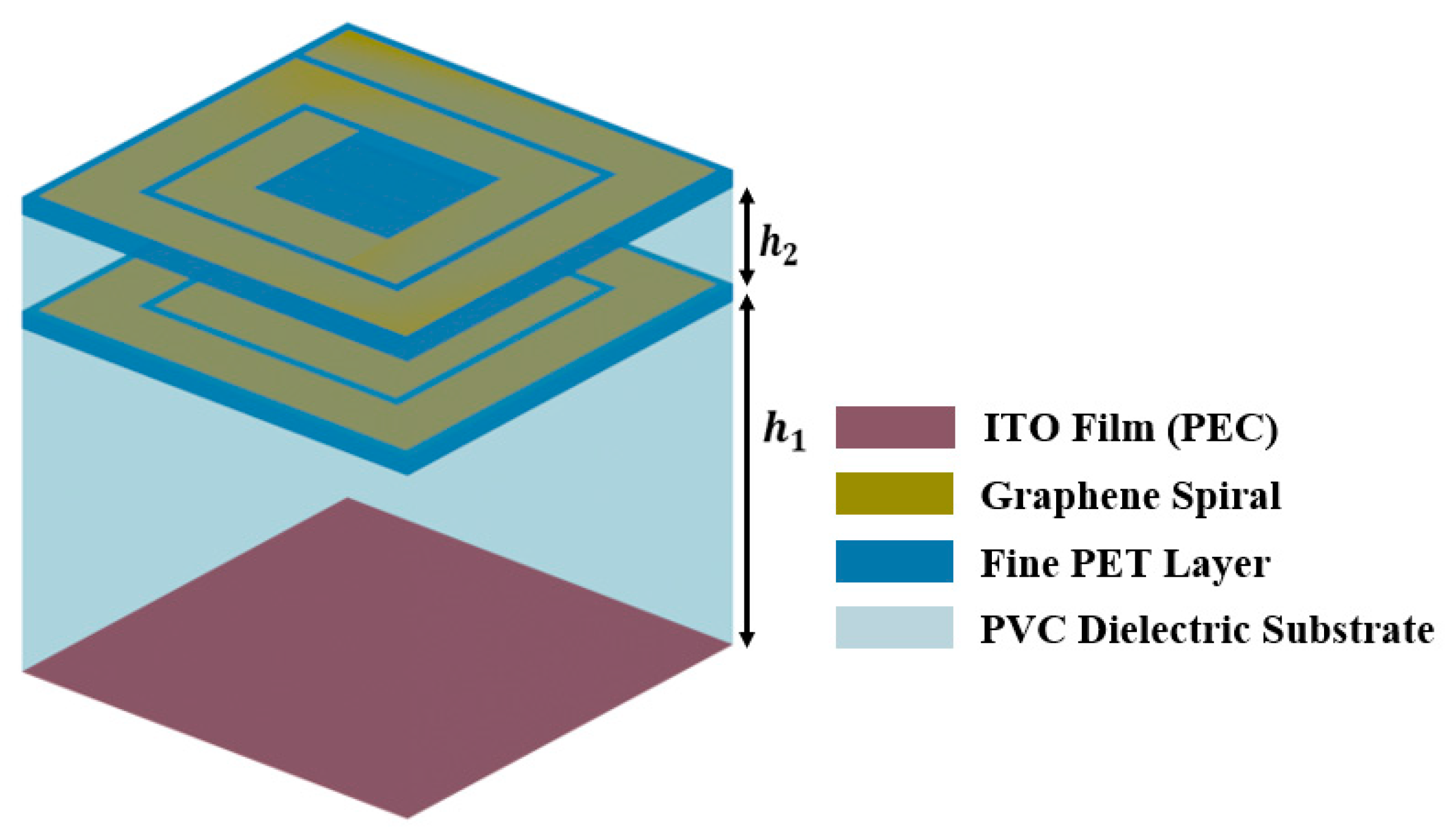
In this section, the ‘stacking graphene metasurface approach’ [
19] is used to broaden the absorption bandwidth. Above the designed GSR metasurface absorber, we place another similar GSR metasurface with a dielectric spacer (PVC) of thickness
. The configuration of this double-layer GSR metasurface absorber (DGSR) is illustrated in
Figure 9. Incorporating two layers of GSR, the controllability of the input impedance of the structure can be enhanced by independently adjusting the Fermi energy of each graphene layer.
The ECM model depicted in
Figure 10 can be used to optimize the DGSR absorber’s performance. The absorbance
of the structure is given by Equation (12), where the input impedance
can be calculated as
The impedance
can be expressed by the transmission line correlation formula as
where
and the impedances
are given by Equation (9). Moreover, to cover the oblique incidence case, the modifications described by Equations (14) and (15) should be made.
The optimized parameters can be determined through an iterative optimization technique using our ECM. Keeping the thickness
equal to one-quarter wavelength in the medium, the thickness
is swept for different pairs of Fermi energies
in the range (0.2 eV–1.2 eV) to find the optimum values that achieve the maximum absorption bandwidth with absorbance
. It is found that, for
and
, a maximum absorption bandwidth of 11.7 GHz is achieved, covering the X and Ku bands.
Figure 11a shows the absorbance spectrum of the DGSR absorber for the case of normal incidence at different Fermi energies
with
.
Figure 11b provides a comparison between the absorbance spectra of the DGSR and the GSR absorbers. As can be seen, taking an absorbance of 90% as a reference, a significant bandwidth enhancement of approximately 3 GHz is achieved. Moreover, the absorber possesses an RBW of about 90%. However, it should be noted that the absorbance of the DGSR absorber is slightly decreased compared with that of the GSR absorber.
The absorption spectra at different incident angles of the DGSR MA are plotted in
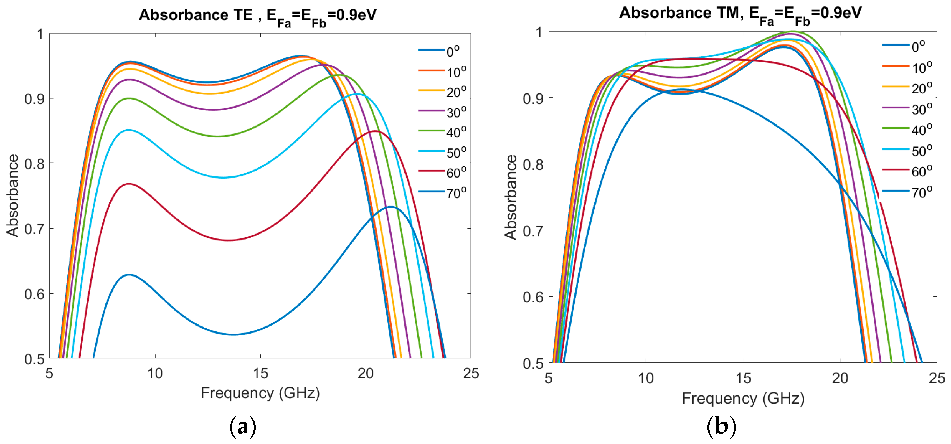
Figure 12a,b for TE and TM incident EM waves, respectively. It is demonstrated that, in the case of the TE wave, the average absorbance remains above 90% for incident angles less than 30°.
The absorbance starts to decrease significantly as the incident angle is increased above 30° however, it remains higher than 80% for incident angles up to 50°. On the other hand, the absorber presents better angle stability for the case of the TM wave, since the absorbance remains above 90% for incident angles up to 50° across the desired frequency range. Overall, the DGSR MA is relatively stable under different incident angles.
5. Discussion and Conclusions
We have designed and analytically studied a tunable microwave MA based on a metasurface made of graphene spiral resonators (GSRs). An ECM described by closed-form equations has been utilized to optimize the structure and demonstrate its absorption performance. The amplitude of the absorption spectra can be modified by applying a bias voltage between the graphene metasurface and the grounded ITO plane, allowing for control over the Fermi energy of the graphene. The whole structure possesses optical transparency and mechanical flexibility, achieved by incorporating transparent and flexible materials. In our design, the lossy GSR metasurface is responsible for the high absorption, since most of the impinging EM energy is dissipated through the induced currents flowing on the resistive graphene spiral resonators. In contrast, the PVC dielectric spacer exhibits negligible consumption of EM waves. Additionally, to broaden the absorption bandwidth, a double-layer GSR (DGSR) is designed using two similar GSR metasurfaces. The optimized DGSR absorber achieves a bandwidth enhancement of roughly 3 GHz, resulting in an RBW of about 90% while remaining ultrathin. Such a BW enhancement has been previously achieved by utilizing thicker structures that share comparable fabrication complexity [
42]. It is worth noting that both absorber designs have a subwavelength thickness (approximately one-tenth of a wavelength), which meets the Rozanov limit [
43], and thus, the validity of our ECM is guaranteed [
44].
Concerning fabrication feasibility, the proposed absorber can be realized using well-established techniques. The monolayer graphene can be grown on copper foil using the conventional chemical vapor deposition (CVD) method. Afterward, the copper foil is etched away. The graphene film is then transferred onto the PET film. However, graphene/PET layers are now commercially available [
26]. The infrared laser beam cutting method can be used to pattern the graphene into a square spiral shape. Next, the patterned graphene can be deposited on the top of the PVC dielectric spacer via a lamination process. Lastly, an ITO film with low square resistance should be attached to the bottom of the structure to act as a ground plane. Some deviations may be found between our simulated results and the experimental ones. There could be discrepancies in the absorbance amplitude and maximum absorbance frequencies. These may be caused by (a) inhomogeneity of the patterned graphene/PET layer sample due to imperfect fabrication; (b) differences in the dielectric constants of the materials from those used in our calculations; (c) the finite size of the fabricated sample, resulting in edge diffraction; and (d) degradation of graphene’s surface resistance due to the presence of impurities in air.
The performance of the proposed GSR and DGSR metasurface absorbers was compared with those of some previously reported graphene-based microwave absorbers, as shown in
Table 1. Evaluated alongside other relevant research, the proposed GSR absorber achieves ultrawideband absorption covering both the X and Ku bands with a relative bandwidth of 68% and high absorbance up to 99.7% at the peaks. Moreover, the designed GSR absorber is characterized by wide-angle stability, optical transparency, mechanical flexibility, and low thickness of 0.09λ, where λ is the wavelength corresponding to the lowest frequency of the absorption band. Furthermore, the designed DGSR absorber has an enhanced absorption bandwidth with a relative bandwidth of 90% and high absorbance up to 97.6% at the peaks. It also remains miniaturized, optically transparent, and flexible. Both GSR and DGSR configurations, due to their attractive features, may have prospects for applications in stealth technology and EM compatibility. Additionally, due to their optical transparency and flexibility, they can contribute to practical applications, including the cockpit windows of low-detectable aircraft and aerospace devices.
