Next Article in Journal
Manchester Return-to-Zero On–Off Keying Modulation for Free-Space Optical Communication
Previous Article in Journal
A Review of Optical Parametric Amplification at the Vulcan Laser Facility
Previous Article in Special Issue
Hybrid Integrated Silicon Photonics Based on Nanomaterials
 
 
photonics-logo
Article Menu

Article Menu

Review

Integrated Photonic Passive Building Blocks on Silicon-on-Insulator Platform

by
Francesco Amanti
1,*,
Greta Andrini
2,3,
Fabrizio Armani
4,
Fabrizio Barbato
1,
Vittorio Bellani
5,6,
Vincenzo Bonaiuto
7,8,
Simone Cammarata
1,9,
Matteo Campostrini
10,
Thu Ha Dao
7,8,
Fabio De Matteis
7,8,
Valeria Demontis
6,11,
Simone Donati
1,12,
Giovanni Di Giuseppe
13,14,
Sviatoslav Ditalia Tchernij
3,15,
Andrea Fontana
6,
Jacopo Forneris
3,15,
Luca Frontini
4,16,
Roberto Gunnella
13,14,
Simone Iadanza
17,
Ali Emre Kaplan
18,
Cosimo Lacava
6,19,
Valentino Liberali
4,16,
Leonardo Martini
20,
Francesco Marzioni
13,14,21,
Luca Morescalchi
1,
Elena Pedreschi
1,
Paolo Piergentili
13,14,
Domenic Prete
6,20,
Valentino Rigato
10,
Carlo Roncolato
10,
Francesco Rossella
6,20,
Matteo Salvato
8,22,
Fausto Sargeni
8,23,
Jafar Shojaii
24,
Franco Spinella
1,
Alberto Stabile
4,16,
Alessandra Toncelli
1,12 and
Valerio Vitali
6,22
add Show full author list remove Hide full author list
1
Istituto Nazionale di Fisica Nucleare (INFN), Sezione di Pisa, 55100 Pisa, Italy
2
Dipartimento di Elettronica e Telecomunicazioni, Politecnico di Torino, 10129 Torino, Italy
3
Istituto Nazionale di Fisica Nucleare, Sezione di Torino, 10125 Torino, Italy
4
Istituto Nazionale di Fisica Nucleare, Sezione di Milano, 20133 Milano, Italy
5
Dipartimento di Fisica, Università di Pavia, 27100 Pavia, Italy
6
Istituto Nazionale di Fisica Nucleare, Sezione di Pavia, Via Agostino Bassi 6, 27100 Pavia, Italy
7
Dipartimento di Ingegneria Industriale, Università di Roma Tor Vergata, 00133 Roma, Italy
8
Istituto Nazionale di Fisica Nucleare, Sezione di Roma Tor Vergata, 00133 Roma, Italy
9
Dipartimento di Ingegneria dell’Informazione, Università di Pisa, 56122 Pisa, Italy
10
Laboratori Nazionali di Legnaro, Istituto Nazionale di Fisica Nucleare, 35020 Legnaro, Italy
11
NEST, Scuola Normale Superiore and Istituto Nanoscienze-CNR, 56127 Pisa, Italy
12
Dipartimento di Fisica, Università di Pisa, 56127 Pisa, Italy
13
Scuola di Scienze e Tecnologie, Divisione di Fisica, Università di Camerino, 62032 Camerino, Italy
14
Istituto Nazionale di Fisica Nucleare, Sezione di Perugia, 06123 Perugia, Italy
15
Dipartimento di Fisica, Università di Torino, 10125 Torino, Italy
16
Dipartimento di Fisica, Università di Milano, 20133 Milano, Italy
17
Paul Scherrer Institute, 5232 Villigen, Switzerland
18
Optoelectronics Research Center, University of Southampton, Southampton SO17 1BJ, UK
19
Dipartimento di Ingegneria Industriale e dell’Informazione, Università di Pavia, 56122 Pisa, Italy
20
Dipartimento di Scienze Fisiche, Informatiche e Matematiche, Università di Modena e Reggio Emilia, 41125 Modena, Italy
21
Dipartimento di Fisica, Università di Napoli “Federico II”, 80126 Napoli, Italy
22
Dipartimento di Fisica, Università di Roma Tor Vergata, 00133 Roma, Italy
23
Dipartimento di Ingegneria Elettronica, Università di Roma Tor Vergata, 00133 Roma, Italy
24
Space Technology and Industry Institute, Swinburne University of Technology, Hawthorn, VIC 3122, Australia
*
Author to whom correspondence should be addressed.
Photonics 2024, 11(6), 494; https://doi.org/10.3390/photonics11060494
Submission received: 10 April 2024 / Revised: 7 May 2024 / Accepted: 14 May 2024 / Published: 23 May 2024
(This article belongs to the Special Issue Photonic Integrated Circuits for Information, Computing and Sensing)

Abstract

:
Integrated photonics on Silicon-On-Insulator (SOI) substrates is a well developed research field that has already significantly impacted various fields, such as quantum computing, micro sensing devices, biosensing, and high-rate communications. Although quite complex circuits can be made with such technology, everything is based on a few ’building blocks’ which are then combined to form more complex circuits. This review article provides a detailed examination of the state of the art of integrated photonic building blocks focusing on passive elements, covering fundamental principles and design methodologies. Key components discussed include waveguides, fiber-to-chip couplers, edges and gratings, phase shifters, splitters and switches (including y-branch, MMI, and directional couplers), as well as subwavelength grating structures and ring resonators. Additionally, this review addresses challenges and future prospects in advancing integrated photonic circuits on SOI platforms, focusing on scalability, power efficiency, and fabrication issues. The objective of this review is to equip researchers and engineers in the field with a comprehensive understanding of the current landscape and future trajectories of integrated photonic components on SOI substrates with a 220 nm thick device layer of intrinsic silicon.

1. Introduction

Silicon photonics, rooted in the Silicon-On-Insulator SOI architecture, has emerged as a transformative technology, revolutionizing various sectors from communication systems to sensing applications [1,2]. Over the past two decades, continuous innovations have propelled the success of silicon photonics, offering unprecedented opportunities for high-speed communication, sensing, and computing. The development of photonic integrated circuits (PICs) on silicon-based platforms, particularly SOI technology, showcases remarkable potential in developing next-generation photonic devices [3] and quantum applications [4,5]. SOI technology, characterized by a thin layer of silicon over an insulating substrate, offers several distinct advantages over traditional bulk silicon and other semiconductor materials. Its thin silicon layer enables efficient light confinement and manipulation, while the insulating layer minimizes optical loss and crosstalk, facilitating the realization of high-performance photonic components. Silicon photonics faces challenges such as fabrication process variations and high losses in coupling between fibers and chips, particularly in sensitive applications like quantum optics. However, by leveraging concepts from solid-state physics and engineering principles, promising avenues emerge for overcoming these fabrication obstacles [6]. One promising approach is to directly integrate single-photon-emitting color centers [7] and single-photon detectors onto the chip [8].
In recent years, significant progress has been made in developing various photonic devices on the SOI platform, including waveguides, modulators, detectors, filters, and light sources, exhibiting remarkable performance metrics suitable for applications in telecommunications, data centers, sensing, and biomedical imaging [9].
By providing a comprehensive evaluation of the current state of the art and a discussion of the challenges and opportunities, this review aims to contribute to the continuous advancement and deployment of SOI-based photonic technologies.
This article is organized based on the following functions:
  • Coupling with external fibers.
  • Splitting devices.
  • Filtering and phase shifting during transmission.
Section 2 explores the coupling of an optical fiber to the photonic chip, with a focus on grating coupling and edge coupling methods. These techniques are vital for minimizing signal loss and enabling efficient light input/output onto the photonic chip. Section 3 delves into switching and splitting functionalities within the chip, discussing devices like directional couplers, y-branches, and MMI devices that are essential for manipulating light signals effectively. Mastery of these techniques is paramount for designing scalable and versatile photonic chip architectures. Section 4 addresses filtering and phase shifting during signal transmission within the chip, covering waveguide crossings, phase shifters, and ring resonators. These mechanisms enable precise control over signal properties, catering to diverse application requirements such as telecommunications and sensing.
To limit the breadth of the topics, we will discuss, except for particularly interesting examples functional to the structure of this article, SOI devices with an intrinsic silicon device layer with a thickness of 220 nm.

2. Coupling with External Fiber

Fiber-to-chip coupling is the stage where the most significant signal loss occurs. It is not always feasible to work with on-chip sources and detectors, necessitating a fiber-to-chip coupling system. This aspect is also influenced by external fiber manipulation equipment and fiber termination (fiber array). In this section, we will discuss the structures that can be constructed on-chip. For an overview of the state of the art up to 2020, we recommend the following specific review papers: [10,11,12]. To address this challenge, two primary solutions are commonly used:
  • Edge Coupling: Referred to as “in-plane”, “end-fire”, or “butt” coupling. Involves directing the light beam in/out of the waveguide through the lateral sides, ensuring propagation in the same plane. It requires high-quality optical facets on the chip sides to achieve efficient coupling (typically exceeding 80%) with minimal polarization dependence.
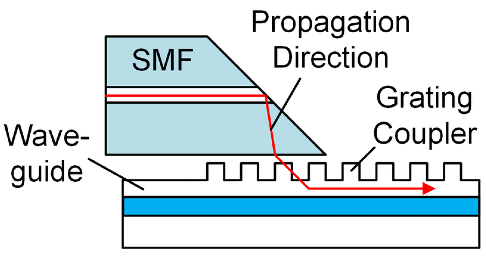
  • Vertical Coupling: In this approach, the light beam is directed onto the top surface of the silicon chip (or the bottom if necessary). A specially designed coupling structure alters the k-vector direction, facilitating the coupling of light into the integrated waveguide. The widely adopted vertical coupling solution relies on diffractive gratings, which are known for their relaxed positioning tolerances, ease of lithographic fabrication, and suitability for multi-point wafer characterizations. However, the simplest forms of these structures inherently exhibit sensitivity to polarization and wavelength, necessitating careful design and optimization to mitigate these limitations. Vertical coupling ensures greater positioning independence at the cost of higher losses. It also enables coupling on the chip surface, facilitating coupling at any point without the need to enter and exit from the edges.
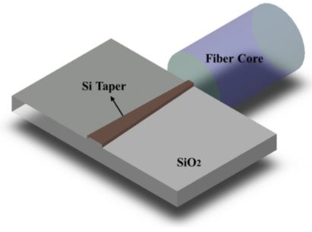
2.1. Edge Coupling

Edge coupling (Figure 1) allows coupling only at the chip’s edges and is highly dependent on the edge cut and fiber positioning. Regarding optical fibers and their terminations, the current trend in edge coupling packaging entails the utilization of high-numerical-aperture (HNA) fibers to optimize the coupling efficiency and alleviate alignment constraints. V-grooves passively place and align the fiber, but they may occupy too much chip area, affecting integration density and cost. Edge coupling’s misalignment tolerance limits its applicability to single-channel packaging, making it costly and time-consuming for multiple fiber connections. Some groups and companies are exploring multi-channel edge coupling for its potential high coupling efficiency [12,13].
The inverse taper is the main and simplest on-chip structure constructed to enhance performance. This design features a waveguide tapering in width along the direction of mode propagation, connecting the narrow end to the fiber and the wider end to photonic waveguides. Modal distribution is determined by both mode order and waveguide structure. Silicon photonic edge couplers primarily focus on the transverse electric (TE) mode, with the commonly used waveguide size supporting TE mode propagation at minimal loss. The gradually varying cross-section area of an inverse taper facilitates mode conversion, allowing it to confine the electromagnetic field inside the taper. In summary, an edge coupler, based on an inverse taper aligned to the fiber core, can effectively convert a large mode from the optical fiber to the compressed guided mode in photonic waveguides. The geometry and the material of the inverse taper zone is the proper building block structure of the edge coupling [14,15,16,17,18,19]. A summary overview of the characteristics of various types of edge couplers is provided in Table 1.

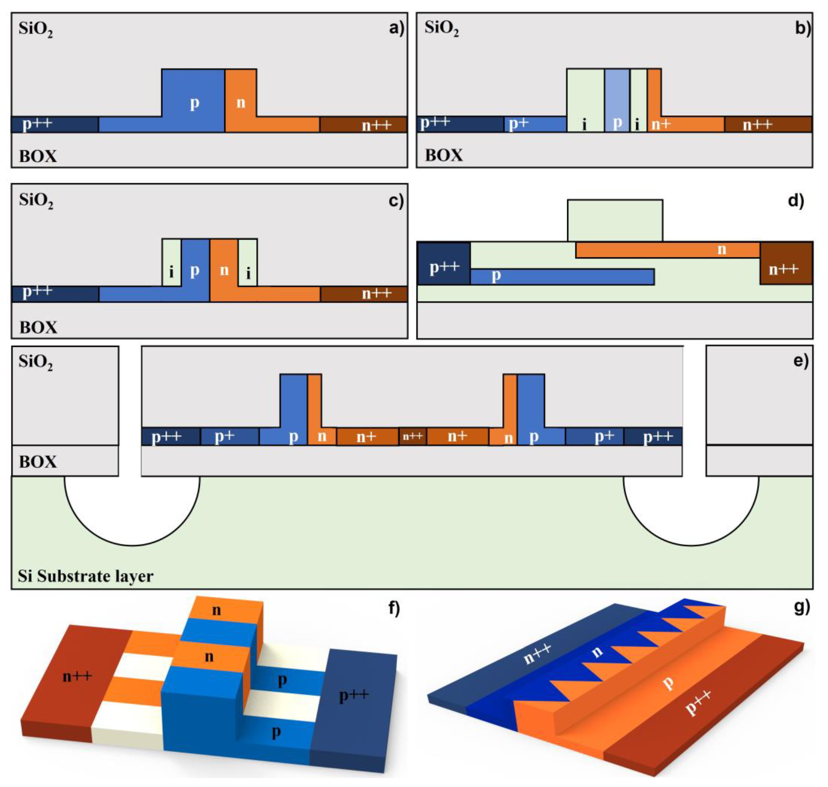
2.1.1. Structural Profiles of Inverse Tapers

Standard inverse tapers have conical form and a length of about 100–500 microns. The fundamental structure for various edge coupler types is an inverse taper that tightens linearly. In this design, the Si waveguide thickness gradually decreases in width toward the fiber, forming a taper. However, the narrow taper end faces challenges in confining light effectively, resulting in a mode distributed over a larger area and an enlarged modal size. Although not always optimal, the linear profile is frequently employed in inverse taper configurations due to its structural simplicity. However, this often results in larger sizes and limited coupling efficiency, especially with fibers that have a large spot size. To address these challenges, inverse tapers can have a nonlinear profile [20,21,22,23,24], including multi-sectional, parabolic, and exponential tapers; these designs are explored for improved performance, emphasizing a smaller footprint, lower propagation loss, and broader bandwidth. In Ref. [25], Ren et al. compared the results about the coupling loss and performance of different inverse taper shapes. The mode spot size decreases with increasing taper length, contributing to enhanced mode confinement. However, as the inverse taper length becomes longer than 200 μm, the coupling efficiency decreases gradually, with length becoming a less critical factor. Linear-shape inverse tapers are preferable for ease of fabrication, while parabolic and exponential tapers excel in achieving lower coupling losses and better misalignment tolerance within a smaller length. Inverse taper-based edge couplers work well only when power efficiency is not strictly required in transmitting light to the photonic circuit. For applications emphasizing power, it is better to use different types of edge couplers.

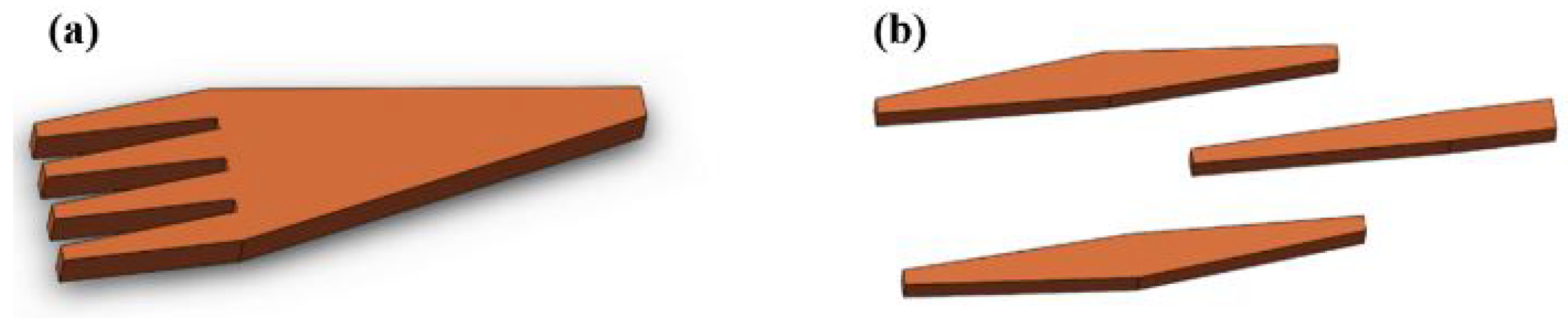
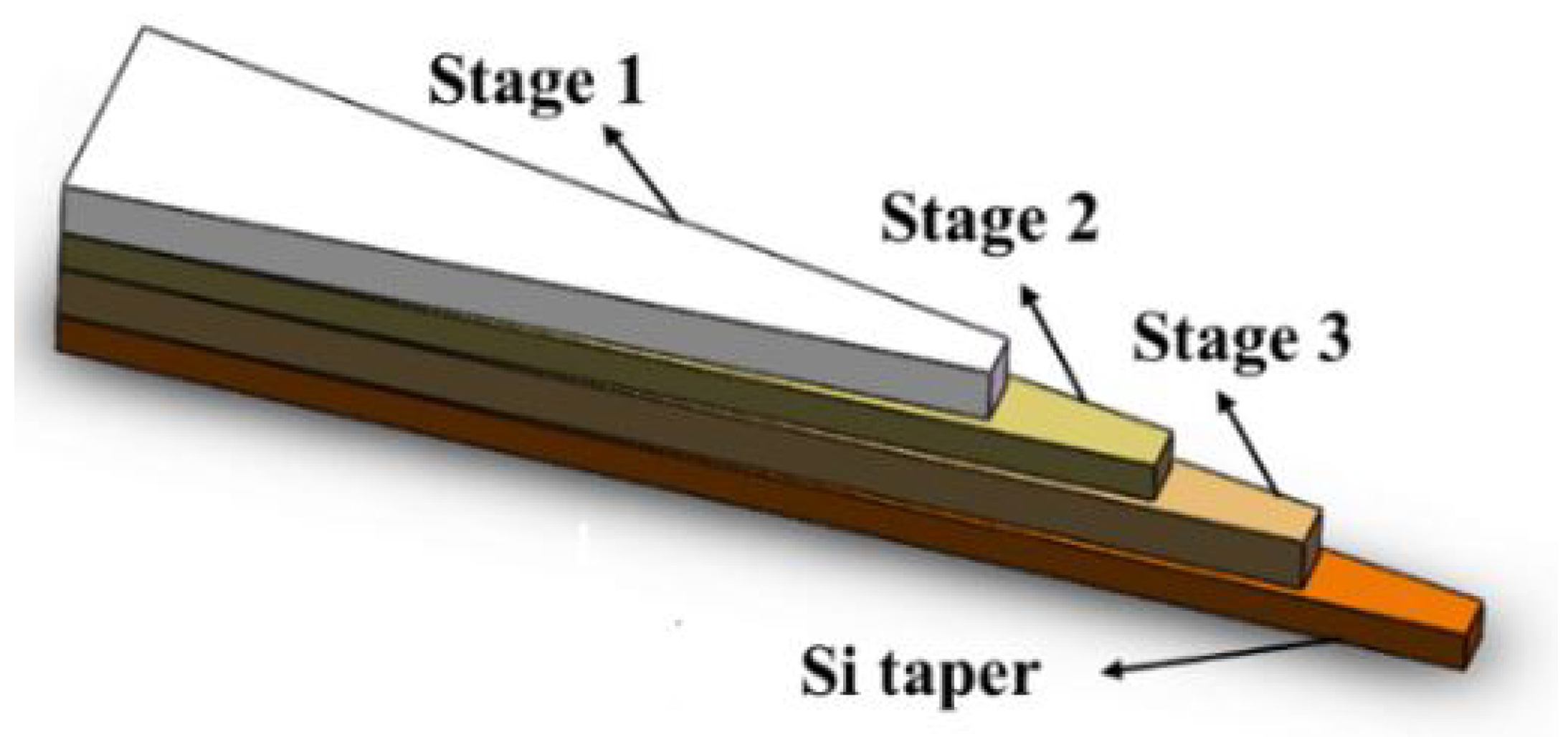
2.1.2. Multi-Tip Tapers and Multiple Tapers

A multi-tip taper with multiple tips can loosen the constraints of alignment and reach larger misalignment tolerance as well as fabrication deviation tolerance. The efficiency of a fiber-to-chip edge coupler is determined by the overlap between the fiber mode and the superimposed mode at the coupler facet, as well as by the mode conversion efficiency. Multi-tip tapers, which feature multiple tips like the ones shown in Figure 2, are commonly used to enhance this overlap efficiency. The modal field diameter (MFD) increases with these tips, improving the match with the fiber mode. Design parameters like tip number, interval distance, tip width, and taper length are adjustable for optimal modal overlap. In fiber-to-chip coupling, precise alignment of the edge coupler facet with the fiber core is crucial for high efficiency. This approach introduces design flexibility to achieve the expected coupling efficiency within a compact footprint [26,27,28,29,30,31].
Taking inspiration from the multi-tip taper concept, a logical next step is to suggest a different type of edge coupler using multiple tapers, as shown in Figure 3. The trident edge coupler, featuring three distinct tapers, is a widely adopted form among various edge couplers with multiple tapers [32,33,34]. An edge coupler with multiple tapers is simple, feasible, and compatible with standard lithography and etching. Like edge couplers with a single multi-tip taper, multiple tapers are more tolerant to misalignment between an optical fiber and the edge coupler compared to a single inverse taper.
The introduction of subwavelength grating (SWG) structures can be applied to the previously mentioned tapers [35,36,37]. The incorporation of secondary wavelength grating structures can achieve a lower effective modal refractive index compared to the Si waveguide on the coupler facet, leading to higher modal overlap with the low-index fiber. The SWG structure offers multiple design variables, providing a high degree of design freedom. Consequently, it is possible to achieve excellent coupling performance, including a high coupling efficiency, compact dimensions, low sensitivity to the polarization state, and a wide bandwidth at the expense of increased fabrication challenges [38].

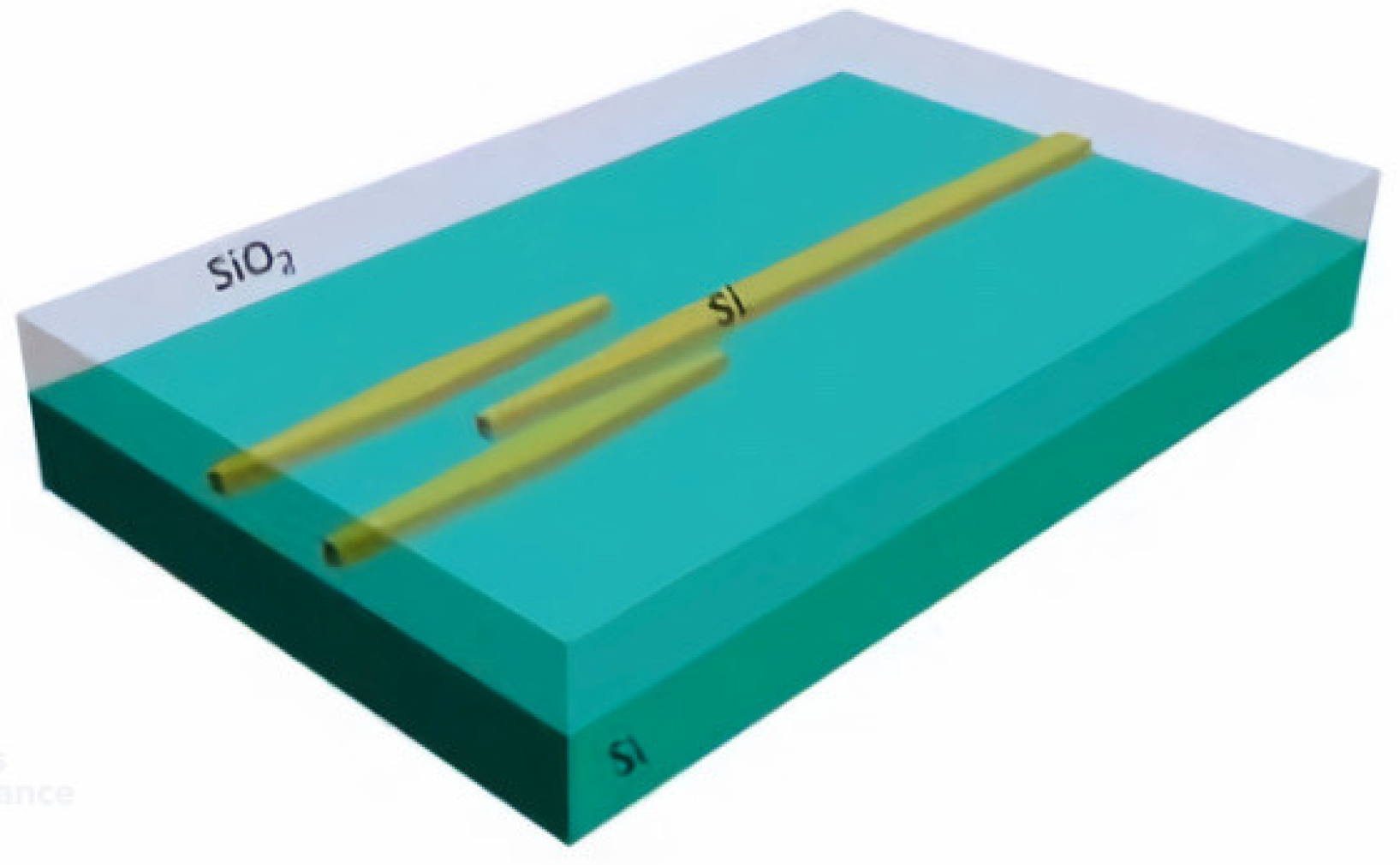
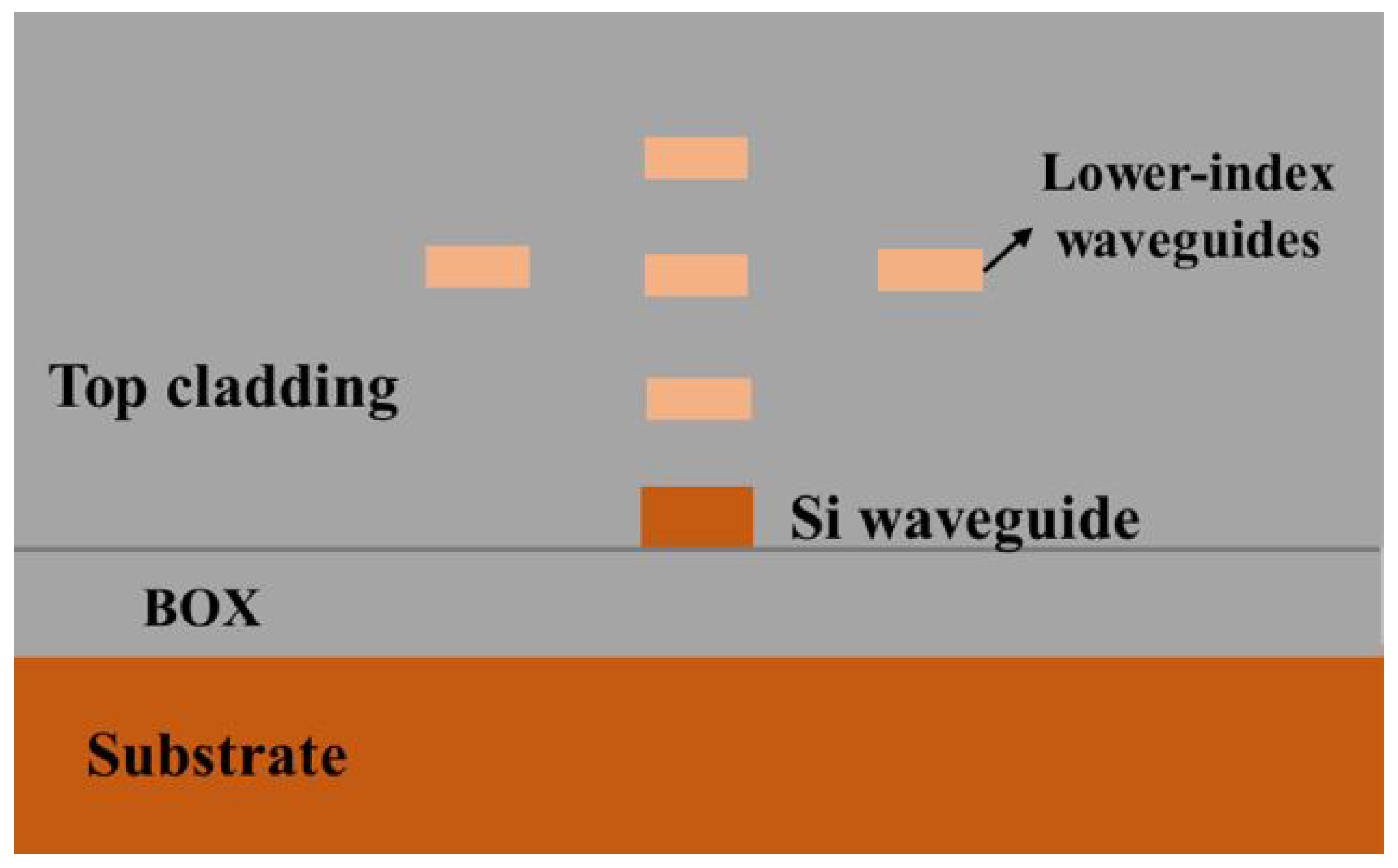
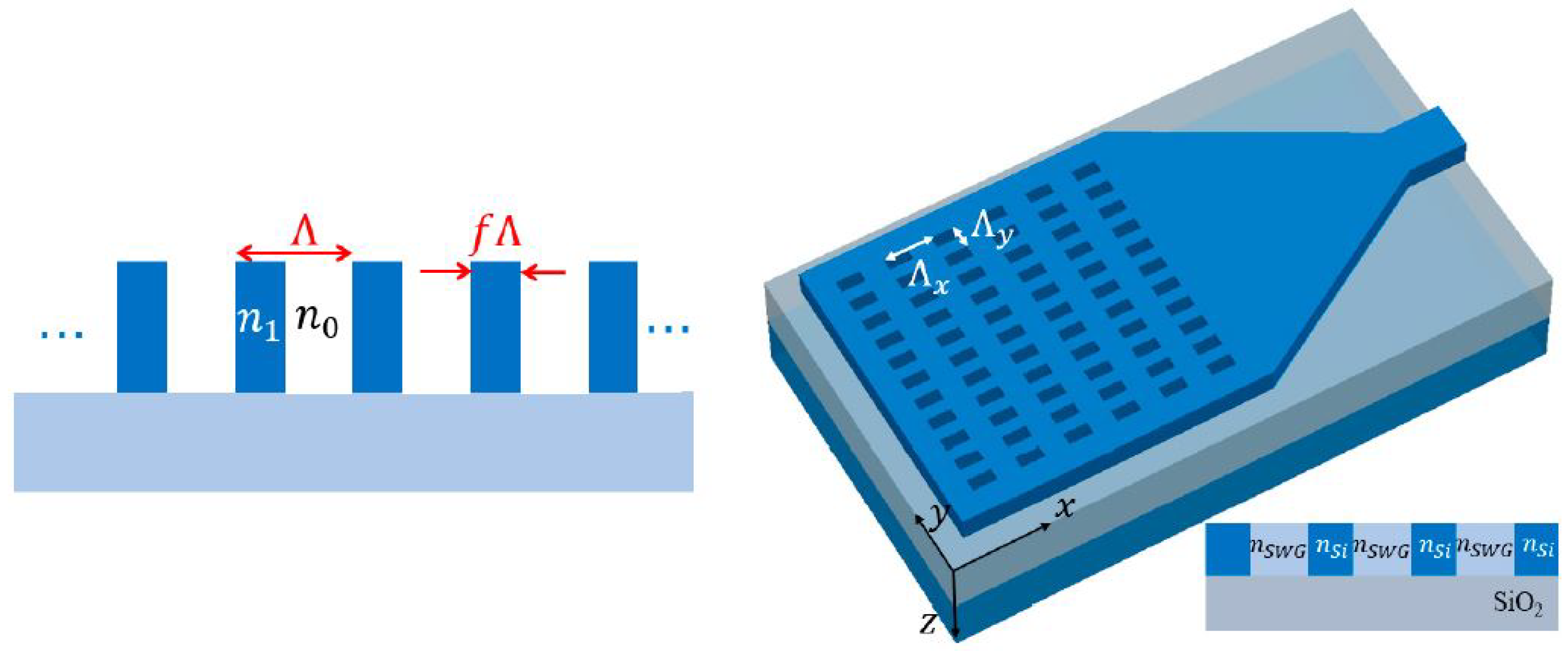
2.1.3. Vertical Multi-Layer Edge Couplers

Multiple Upper Waveguides, index-matching cladding, cascaded multi-stage tapers, and Three-Dimensional Tapers are vertical structures, orthogonal to the fiber-waveguide direction. The primary objective is to expand the effective modal area vertically, ensuring a robust modal match with the fiber core and the coupler facet.
Multiple Upper Waveguides [39,40], which are typically made of materials with lower refractive indexes than silicon, like silicon nitride (SiN) and silicon oxynitride (SiON), ensure compatibility with the SOI platform and CMOS fabrication. An example of this design is represented in Figure 4.
However, challenges arise in the design. Alignment complexities must be addressed during the deposition of each layer, including the lateral alignment of upper assisting waveguides with the Si inverse taper for proper modal distribution. Interlayer alignment becomes crucial as assisting waveguides are positioned at various heights, requiring careful achievement of the required waveguide pattern. Despite these challenges, a novel spot size converter, assisted by upper SiON waveguides, has been demonstrated to achieve a nominally low loss of 0.4 dB over a total length of 450 μm [41]. This novel design reduces the complexity of the alignment and fixation of a single mode fiber to photonic chips, but it is quite challenging for fabrication feasibility and further practical applications.
Cascaded multi-stage tapers consist of multiple unidirectional tapers in different layers with their wide end near the fiber and their narrow end close to the waveguides.
At the wide end, where tapers from different layers converge, the edge coupler features a large cross-section area comparable to the fiber core. In multi-stage tapers, the top layer has the shortest taper length, and the bottom layer has the longest, as shown in Figure 5. As light propagates through these cascaded multi-stage tapers, it reaches the first taper tip where the top-layer taper ends, and due to a small cross-section area, it tends to transmit into the successive layer below with a higher refractive index than the surrounding SiO2 cladding. This pattern continues as light propagates, reaching the bottom layer that connects with the silicon waveguides. The quantity of stages in a cascaded multi-stage edge coupler is unconstrained but too many layers will increase the fabrication complexity with excessive deposition and lithography steps. Too-few layers may lead to insufficient mode conversion into the critical silicon layer. In the literature, bilayer tapers completely made of silicon can be found, which are simple to manufacture [42,43,44]. Generally, if several materials are used, as in Figure 5, three to five layers are most commonly used for cascaded multi-stage tapers [45,46,47].
Tapers buried in index-matching claddings are another technique that is not so different from two-stage tapers. A spot size converter buried in the cladding can be composed of different polymers [48,49], with the most widely used being SU8 [50,51,52], amorphous silicon [53], and SiON materials [54,55]. In recent times, 3D-structure tapers have gained popularity, as highlighted in references [56,57,58]. Despite facing challenges such as losing Y symmetry and encountering fabrication issues, these tapers show low coupling losses. Zhao et al. [59] proposed a design for a spot size converter that integrates an ion-implanted graded index waveguide (GRIN) with a 2D inversely tapered waveguide. This design aims to facilitate the efficient coupling of light between a cleaved single-mode fiber and a silicon waveguide. The device demonstrates a low coupling loss of 0.29 dB for TE mode and 0.27 dB for TM mode. Brunetti et al. [60] proposed a very-high-performance spot size converter that can produce losses of 0.18 dB for TE mode with a 600 μm length and 0.6 db for TM mode with a 600 μm length. The fabrication procedure carried out at LioniX International BV is explained in the article. Cantilevered structures are commonly used in micro-electromechanical devices (MEMSs) and play important roles in edge coupler design. A suspended Si taper clad with SiO2 is exposed by undercutting the BOX layer and the substrate beneath it to a certain thickness, starting from an initial single Si inverse taper. As discussed in Ref. [61], staggered structures are difficult to automate and therefore the distribution of these couplers is limited.
Table 1. Overview of edge couplers with different structures.
Edge C. ConfigurationCoupling Loss (dB)PolarizationSize (µm)Manufacturing Process
Taper with linear profile [25]1.37/2.13TE/TM250/200simple
Taper with exponential
profile [25]1.37/2.12TE/TM170/140simple
Taper with quadratic profile [25]1.39/1.87TE/TM170/150simple
Edge double-tip inverse
taper [31]1.10/1.52TE/TM40intermediate
Trident edge coupler [34]<1.5/<1.7TE/TM300intermediate
GRIN waveguide with a 2D inverse taper [59]0.29/0.27TE/TM300very hard
Silicon nitride spot size converter [60]0.18TE600medium
Nano-taper coupler cladded with SU8 cladding [50]0.5/0.9TE/TM300simple but expensive
Compact cantilever
coupler [62]0.62/0.50TE/TM7very hard
Sustainable 3D edge couplers [58]0.70/1.34TE/TM55hard
0.80/1.60
1.00/1.14
Buried 3D spot size
converter [57]0.54TE100very hard

2.2. Vertical Coupling

The widely adopted vertical coupling solution relies on diffractive gratings. Characterized by relatively relaxed positioning tolerances and ease of lithographic fabrication, they allow for multi-point wafer characterizations.
Vertical coupling solutions are highly sensitive to polarization and wavelength, and various structures and geometries have been developed to manage this sensitivity.
A grating, in the context of SOI-based photonic chips, is an often periodic pattern of materials or structures on a surface. It is created by etching on SOI or selectively depositing amorphous silicon on SOI, causing a refractive index variation. If the index variation’s period is larger than the light wavelength, the diffraction effect prevails; otherwise, it behaves like a uniform medium. Grating couplers (GCs) operate in the diffraction regime.
A 1D-GC, with index variation in one direction, couples light in that direction. Straight-grating GCs require a spot size converter, while confocal gratings enable compact GC design. The same principles apply to 2D-GCs if only one direction works in the diffraction regime; if both directions work, light can propagate in both, with 1D-GC principles applying to each.
The behavior of a grating coupler is explained in Figure 6 and can be described using the phase matching condition, which aligns the wave vector of incident light with the vector of the light beam propagating in the waveguide. We omit the mathematical details of the Bragg equation, as they have been presented in several reviews [11,12].
A summary overview of the characteristics of various types of grating couplers is provided at the end of this section in Table 2.

2.2.1. Parameters of Grating Couplers’ Structures

Consider a planar waveguide grating structure with grating material index n 1 , gap material index n 0 , period Λ , and fill factor f, like the one shown in Figure 7. The size of a focusing grating coupler is influenced by the section angle ( α s ) after setting the grating curve. To reduce the footprint, a larger α s can be chosen, but this might lead to increased roughness due to lithographic representation as polygons, causing extra scattering loss. Achieving a balance is necessary, considering fabrication constraints and minimizing footprint while managing potential roughness-related issues.

2.2.2. Coupling Strategies

There are two commonly used vertical coupling techniques [63,64,65]. One is direct vertical coupling [66], usually with an inclination from 0° to 10°. The fiber is tilted relative to the normal direction of the plane by a maximum of 10 degrees in the direction in which the light is to be injected, so that the plane formed by the fiber and waveguide is perpendicular to the chip plane. In cases of bidirectional grating couplers, the light will be injected in a completely vertical direction. The distance of the fiber end from the chip is usually macroscopic. This setup offers the advantage of leveraging three-dimensional space using fiber holders positioned at various heights, thus keeping the chip surface unobstructed. The disadvantage is the presence of losses due to the optimization of coupling.
The other technique is quasiplanar coupling [67]. A v-groove array is positioned above and in contact with the chip, and the light is reflected from the end of the chip to a specific point where the input or output grating coupler is located, as shown in Figure 8. The advantages of this technique are robust fixation and rigidity, but it requires the use of the chip surface, necessitating the avoidance of crossovers and overcrowding with other elements on the surface.

2.2.3. Multi-Layer Grating Coupler

Diffraction gratings on the SOI face limite directionality due to similar refractive indices in the superstrate and buried oxide. To improve directionality, the grating structure is modified to create constructive interference upwards and destructive interference downwards [69,70], as shown in Figure 9a. The thickness of the oxide layer can be adjusted for constructive interference (see Distributed Bragg Reflector technology [71]); alternatively, a highly reflective material, like a thin metal layer, can be buried below the grating [72] (see Figure 9b). However, building localized multi-layer structures involves complex fabrication methods.

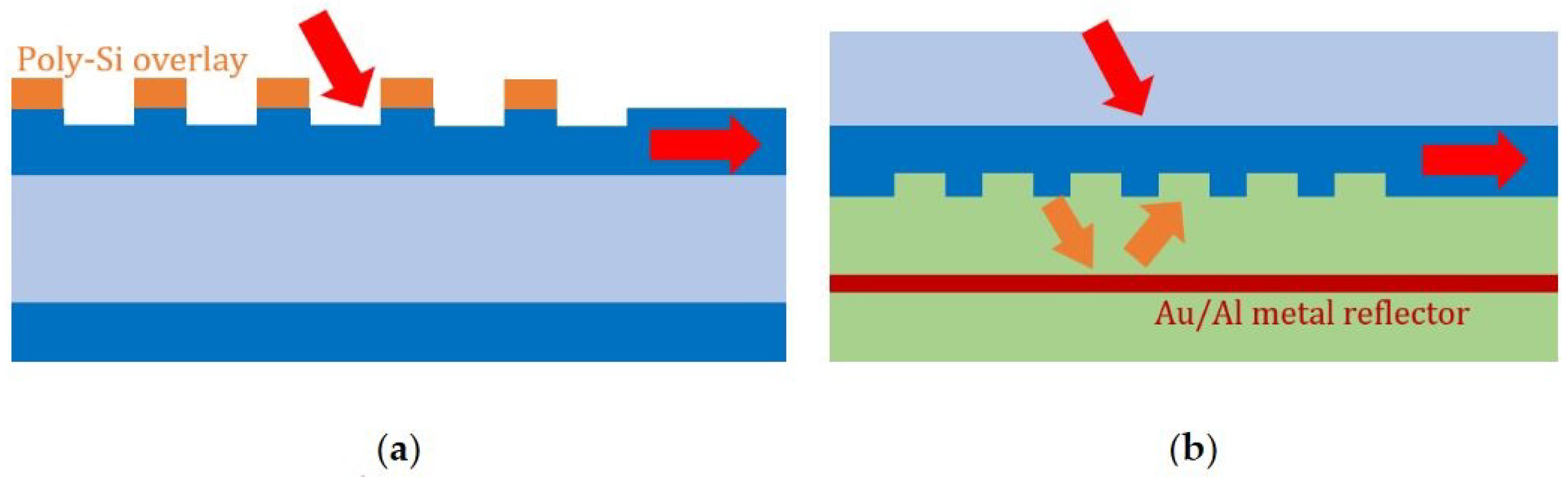
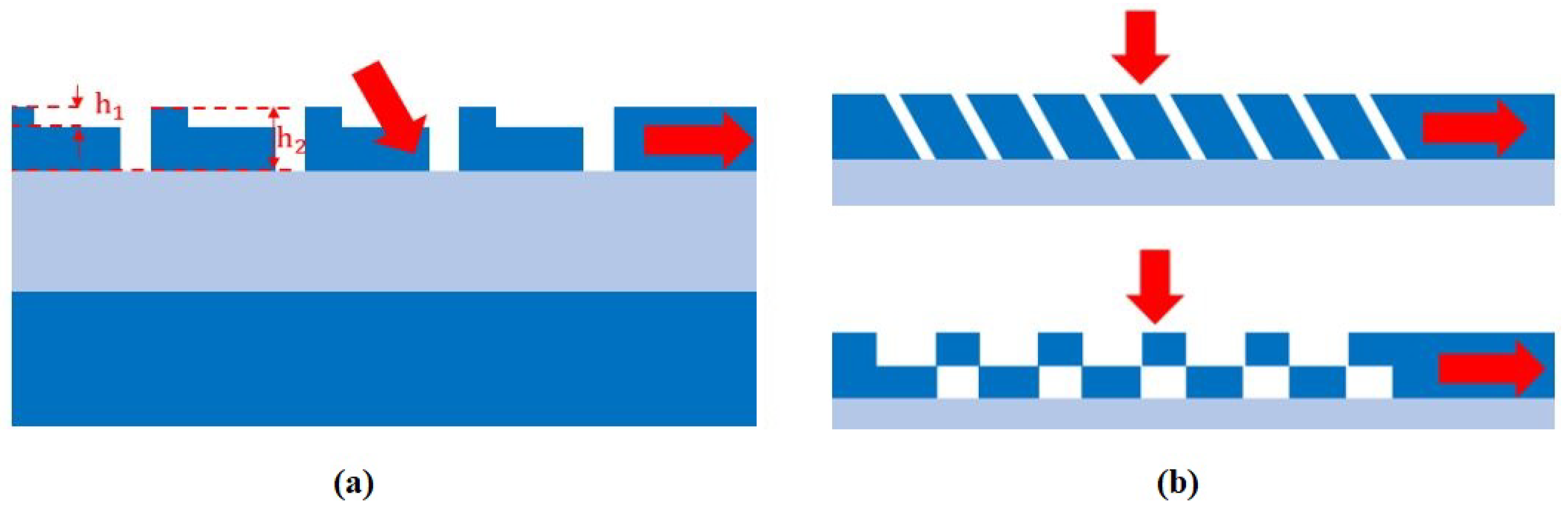
2.2.4. Grating Structural Innovations

Modification of the geometry of the grating brings significant improvements to transmission, and various techniques have been proposed in the literature. The shallow grating coupler has established itself as the norm [73,74]; however, more complicated shapes, such as multiple etching shapes [75] (see Figure 10a) permit a few very efficient mode transmissions. Furthermore, altering the pitch of the grating and apodization of the grating are very common techniques to improve GCs. A general theoretical approach to optimize the pitch is presented in [76]. We can build a GC that operates as a wavelength filter [77] with irregular pitches. Slanted GCs [78,79] (see Figure 10b) are not as widespread as the previous ones due to manufacturing difficulties. Oblique profiles require the use of the Focused Ion Beam technique, and have long development times.

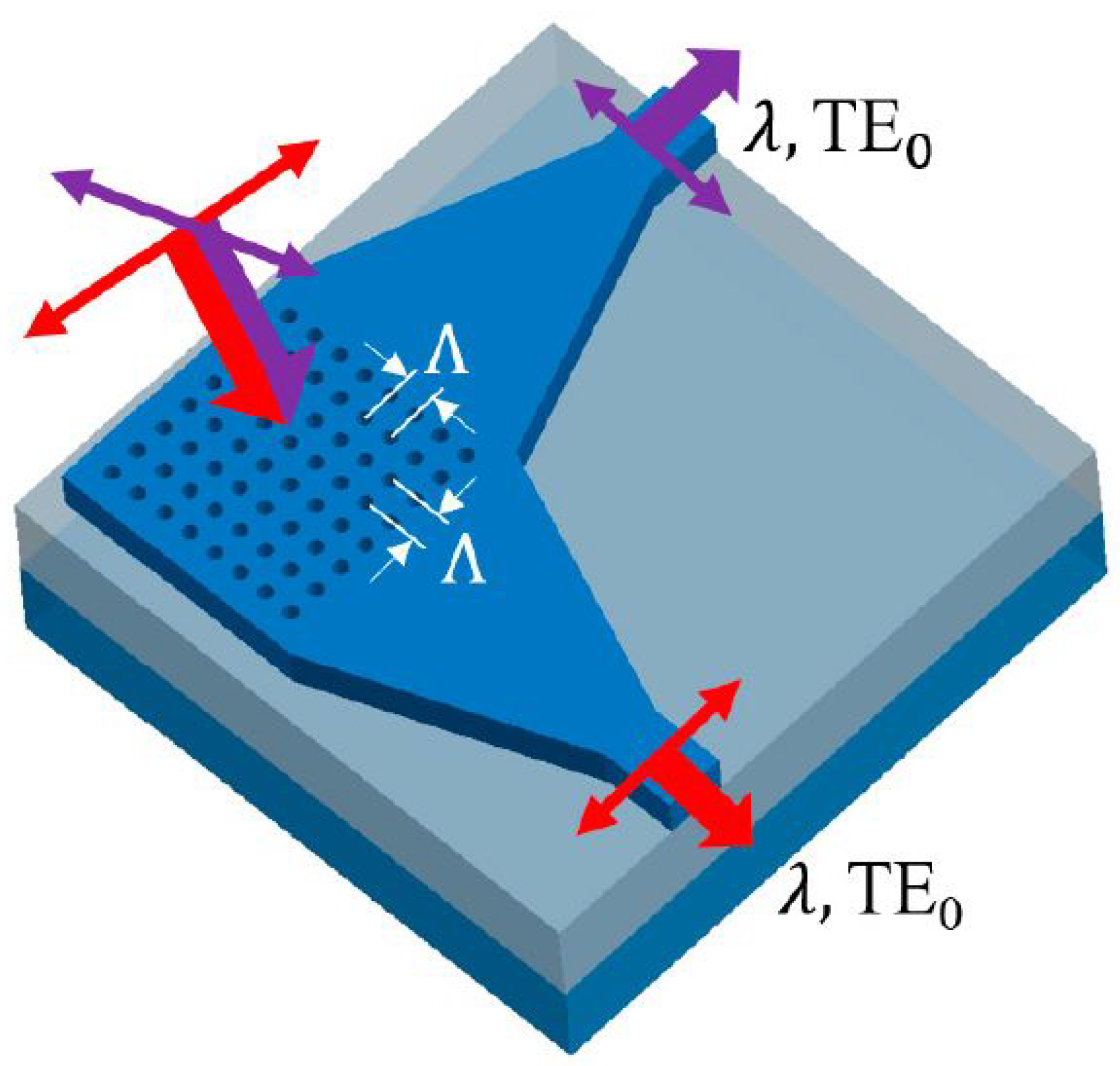
2.2.5. Two-Dimensional Grating Couplers

A 2D Polarization Splitting Grating Coupler (PSGC) [80,81] combines two 1D-GCs arranged orthogonally, each efficiently guiding the light of its respective polarization into the TE mode within the associated waveguide, as depicted in Figure 11. When light enters from a fiber with any polarization, it splits into two orthogonal linear components. These parts can then be transformed into TE modes within two separate waveguides. Even if the polarization changes, the total power coupled into the two waveguides remains nearly the same, making the 2D PSGC polarization-insensitive.
Table 2. Overview of different grating couplers.
Grating C. ConfigurationExperimental C. Loss (dB)PolarizationBandwidthTo Be Modified
Shallow etched grating coupler [73]3.1TE44 nm 1 dBsimple
Poly-Si overlay [69]1.6TE33 nm 1 dBsimple
Non-uniform shallow etch depth 70 nm [82]0.8TE75 nm 3 dBsimple
GC dual band // demultiplexer [83]4.9TE81 nm 3 dBintermediate
Slanted grating couplers fabricated by FIB [79]3.32TE80 nm 3 dBintermediate
Grating couplers with backside metal mirrors [72]0.5TE40 nm 1 dBvery hard
Double etch L-shaped grating [75]2.7TE62 nm 3 dBsimple but expensive
Apodized shallow grating coupler [74]2.7TE41 nm 1 dBvery hard

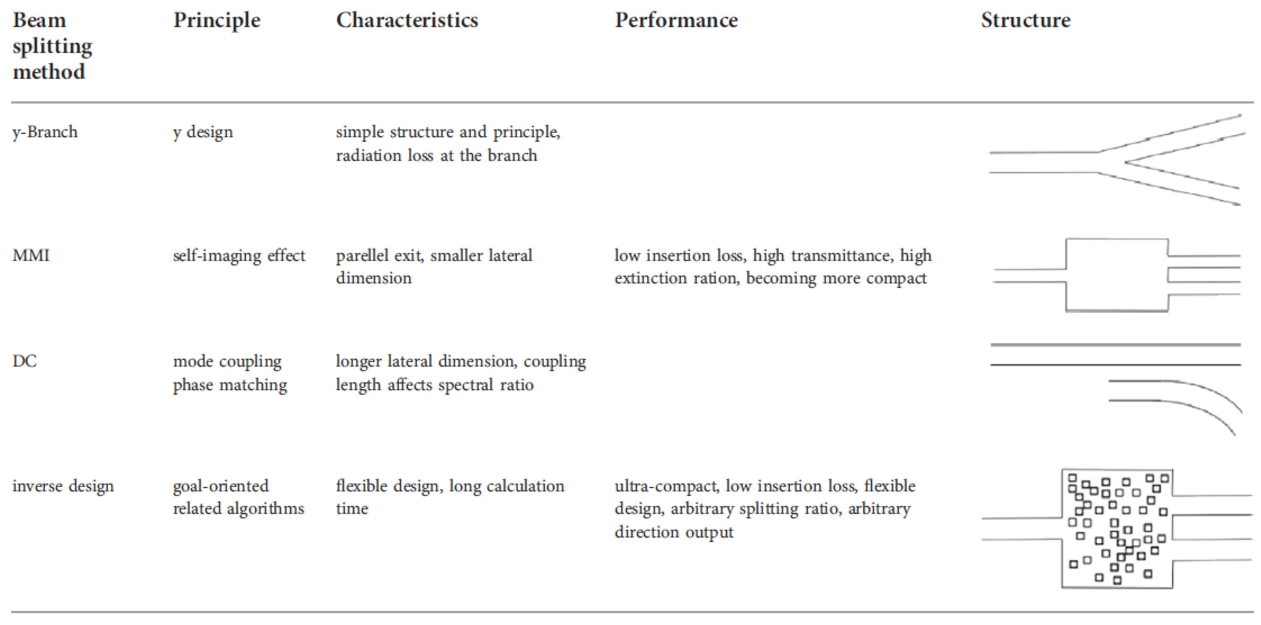
3. Splitting Devices

To separate and divide the signal, a bifurcation is introduced into the optical path. When encountering this junction, a beam is split in different paths. This process is described by defining two coefficients, denoted as T and R. The ideal values for these coefficients are within the range 0 T 1 , with the constraint T + R = 1 .
If T + R is less than one, it indicates losses, and the signal is either reflected within the fiber or is dispersed outside the fiber. Enabling the modulation of these switches through an external signal is one of the active components found in chips. The modulation principle is based on interference, and the devices can be thermal, electrical, or path-based. To separate or direct beams, three types of structures are employed:
  • Y-branches.
  • Directional couplers.
  • Multimode interferometer and inverse design devices.
In Figure 12, we find a schematic description of the different kinds of devices. The coefficients T and R depend on the mode (TE or TM) of propagation in the physical structure. In addition to the fabrication challenges, the fundamental parameter for a high-quality splitter are the losses in single-mode transmission, which must be minimal. We will only discuss SOI splitters at 1550 nm; for other platforms and wavelengths, we refer to the 2022 review [84].

3.1. Y-Branch

The y-branch splitter, considered one of the fundamental integrated optical devices, comprises a single input waveguide and two output waveguides, effectively confining a beam for distribution and propagation along the y-axis. Achieving uniform power splitting is facilitated by employing a longitudinally symmetric design for the y-branch, allowing for optimization of its basic structure. Additionally, the integration of specialized structures onto the conventional y-branch enables the realization of enhanced functionalities, including polarization beam splitting. Y-branch splitters have compact dimensions below 10 × 3 μ m 2 , but introduce some radiation losses at the branch point ([0.01–: 0.1 dB]).
Typically, the performance of these devices is strongly influenced by the polarization of the radiation. However in 2019 [85], a significant advancement occurred with the development of a polarization-independent beam splitter using SWG structures. The design features a compact 8.5 μm coupling length, strategically positioning SWG structures on both sides of the central input waveguide and the inner sides of the two outer waveguides. These integrated SWG structures markedly boost coupling strength for the TE mode while having minimal impact on the TM mode. Experimental results showcase impressive performance, including an insertion loss (IL) of 0.1 dB (0.085 dB) and a reflection loss (RL) of 39 dB ( 46 dB) for TE (TM) mode at a 1.55 μm wavelength. More polarization-independent splitters are described in [86,87,88,89] and in the 2023 review [90]. Contrarily, there are geometrically different splitters that allow the separation of the TE mode from the TM mode [91,92]. The device [93], developable through lithography, consists of a silicon layer with a hole array, demonstrating that the polarization insertion loss is less than 2.98 dB at 1550 μm, and the extinction ratio reaches values greater than 22–27 dB for the TE output port and 16–22 dB for the TM output port within a bandwidth of 110 nm. The efficient wavelength range covers the telecom band from 1500 to 1630 μm. Ugo et al. [94] developed a highly efficient mode splitter. This mode splitter can be fabricated with just one lithography step and demonstrates excellent fabrication tolerances. Experimental findings reveal that the device achieves cutting-edge performance with insertion loss below 0.9 dB and cross talk exceeding −16 dB across a wide bandwidth from 1500 to 1600 nm.

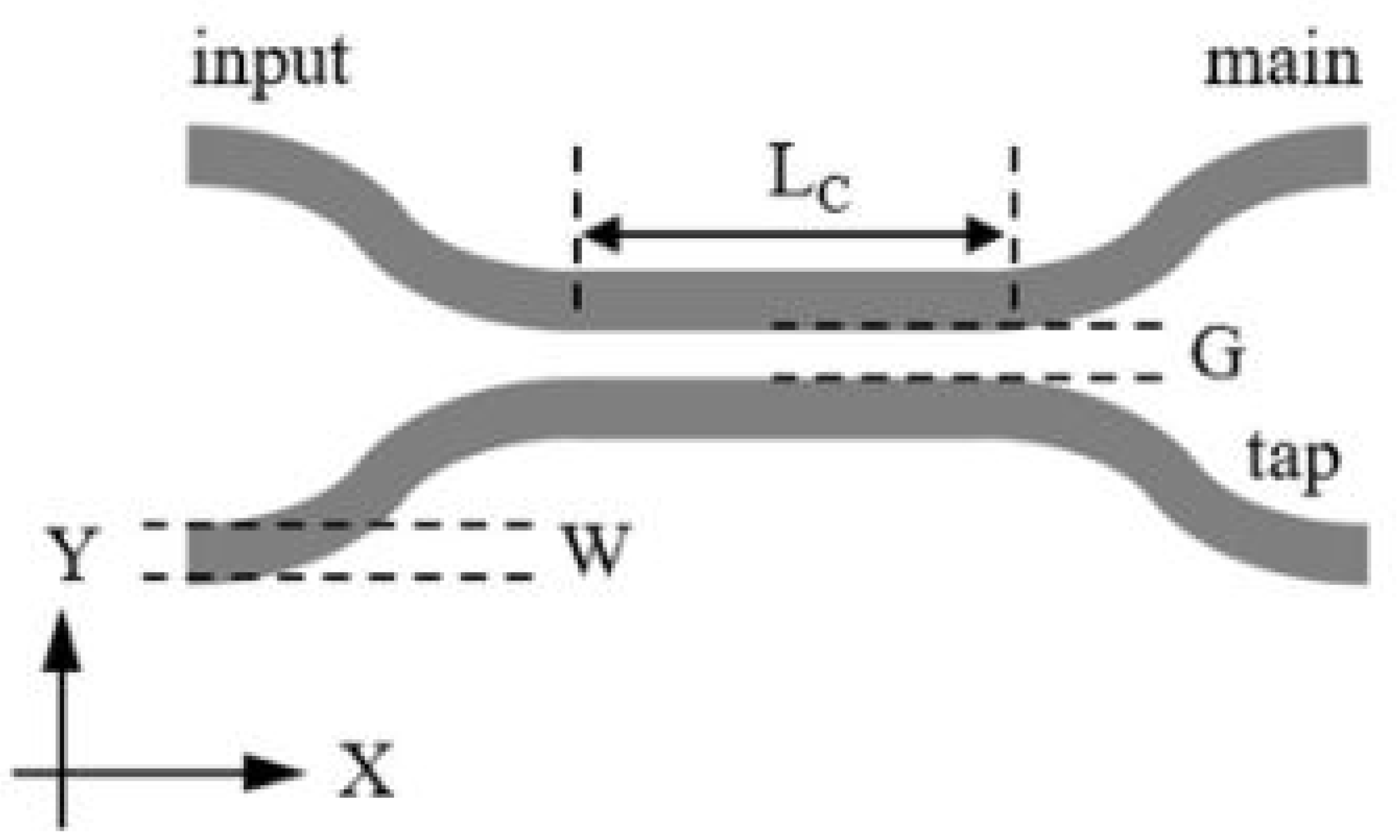
3.2. Directional Coupler

The directional coupler serves the purpose of interfering with the signals from two input channels, generating an output across two channels. Two waveguides approach each other with a gap width smaller than half the wavelength. The length of the interval over which the waveguides run parallel at the gap distance (G) is referred to as the coupling length (Lc) (see Figure 13). This configuration causes the wave propagation to transition from a single mode on a 220 nm guide to a superposition of higher-order modes, one even and one odd, on a wider guide. Consequently, an oscillation of the electric field occurs between the two waveguides.
To analyze this physical entity, a 2 × 2 matrix is employed for computation. The use of asymmetric physical entities enables the realization of a splitter that is highly dependent on the input channel (one or two), exhibiting low crosstalk values (20–30 dB) and insertion loss below 1.2 dB [96]. Splitting via the directional coupler allows for achieving variations in transmission/reflection (T/R) near one. Extremely low values of insertion loss (−0.27 dB) are observed, as discussed in Ref. [95]. The exploration of different shapes for directional couplers, such as asymmetrical bent directional couplers [95,97,98,99] or bridged silicon wires [97,100,101], enables the enhancement of component performance or the creation of polarization beam splitters. To achieve tunability with temperature, coupling coefficients can be manipulated using alloy arrangements, transitioning between a crystalline and amorphous state as the temperature varies, making the system tunable [102].
SWG structures within directional couplers offer an effective approach for achieving polarization-independent power beam splitting [85,103]. Although metamaterial structures in the form of SWGs pose fabrication challenges, they enable the creation of an increasingly diverse range of high-performance devices operating at near-infrared telecommunication wavelengths across various components, as highlighted in recent reviews [104,105].
A directional coupler fully suspended in air can serve as a basic building block for large-scale silicon photonic micro-electromechanical system circuits [106]. Polarization-independent splitters can be constructed using the directional coupler principle, as we have already discussed for y-branches [107]. In 2023, a multi-output 3D, multi-output, 1xM directional coupler-based splitter was proposed [108].
Brunetti et al. proposed a comprehensive switch [109] utilizing a directional coupler that can be tuned by a heater. In Section 4.2.2, we will delve into the construction of the heater as a fundamental component of the thermal phase shifter.

3.3. Multimode Interferometer (MMI) and Inverse Design Devices

Multimode interferometers (MMIs) serve as crucial components in the enhancement of high-performance transceivers, aiming to elevate the data transmission capabilities of prospective detector systems. Their application is dictated by the distinctive power splitting ratio inherent to MMIs, designating them for specific roles in both Mach–Zehnder modulators and the facilitation of precise working point control. This allocation aligns with the strategic utilization of MMIs to optimize signal modulation within transceivers, contributing to the overall advancement of data transmission capabilities in forthcoming detector systems. MMIs enable 1 × N power splitting with customizable split ratios for each output, which is achieved through optical path interference. Unlike y-branch configurations, the MMI operation is elucidated through the distinct propagation velocities of TE and TM modes, causing interference at the output guides, leading to a controlled separation. A more comprehensive theoretical discussion on the operation of MMIs is presented in [110]. In Ref. [111], two types of the standard 3-dB compact structures shown in Figure 14, with dimensions around 25 × 5 μm, are presented and compared with other devices.
Conventional and easy fabrication design demonstrates greater wavelength independence, making them suitable for operation within the 1550 nm range as well as the 1500–1600 nm and 1950–2050 nm wavelength bands [112].
A very easy to build and essential design of polarization beam splitters (PBSs), based on MMIs, is explained and tested in [113]. Other PBSs constructed through MMIs show larger dimensions compared to y-branch and directional coupler devices [114,115].
An insensitive power splitter 1 × 2 based on MMIs is presented in [116], while an SWG MMI 1 × 2 utilized as a mode-insensitive phase shifter is discussed and tested in [117].
A semi-analytical method for calculating S-parameters in general N x M MMI couplers is introduced in [118].
The method, based on mode decomposition and an effective index approach, approximates the channel waveguide using an equivalent slab waveguide with exact analytic expressions for its modes.
Alternatively to the direct approach, inverse design devices are conceived with a specific focus on their intended function, wherein the multimode zone can adopt varied shapes and profiles for optimization according to the desired splitting ratio or desired function. See Figure 15 and the explanations described in [119,120].
MMIs are well suited to the inverse design technique; in Ref. [121], a one to four inverse architecture for MMIs is introduced that allows for arbitrary split ratios with minimal losses (<1 dB). The proposed structures exhibit noteworthy sensitivity to wavelength variations, with the split ratio showing substantial changes in response to even minor wavelength fluctuations compared to classical MMIs.

4. Transmission and Signal Perturbation

During transmission along the waveguide, the signal in single mode can experience losses, reflections, wavelength shifts, or phase shifts, resulting in variations in the optical path or the refractive index. These effects can be non-negligible since we are focussing on the 1550 nm near-infrared (NIR) region.

4.1. Waveguide Technology

The characterization of the silicon waveguide and the creation of a standard was developed in the first decade of this century [122]. The high index difference ( Δ n 2.0 ) between silicon and silicon dioxide enables the creation of waveguides with sub-micron cross-sections and bending radii of less than 5 μm [123]. Nonetheless, the scattering losses resulting from uneven sidewalls increase with the third power of the refractive index difference ( Δ n 3 ) [122], leading to considerable propagation losses in silicon nanowaveguides. The roughness on the sidewalls primarily stems from imperfections in photolithography and etching techniques. Sophisticated fabrication equipment with high resolution capabilities is often necessary to create silicon nanowaveguides with features smaller than a micron. These tools aid in refining the sidewalls and minimizing scattering losses. CMOS technology with deep ultraviolet lithography provides the necessary precision and efficiency for mass production, showcasing its capability. Using this technology, in 2004 [124] Vlasov et al. obtained propagation losses of 3.6 ± 0.2 dB/cm in TE polarization and in 2014 [122] Qiu et al. proposed an optimized design with 2.4 ± 0.2 dB/cm (TE) and 0.59 ± 0.32 dB/cm (TM).
For a complete review of different shapes and materials, please refer to Mashanovich et al. [125] and Selvaraja and Sethi [126]. The best results presented are 0.6 dB/cm for a strip waveguide and 0.2 dB/cm for a rib profile for TE mode.

4.1.1. Bending Losses

FDTD simulations of bending losses by Sheng et al. [123] confirm the experimental results measured by Vlasov et al. in 2004 [124]: for TE mode, bending losses are 0.005 dB/turn, 0.013 ± 0.005 dB/turn, and 0.086 ± 0.005 dB/turn, respectively, for bending radii 5 μm, 2 μm, and 1 μm. In [123,124], the bending losses resulting from FDTD simulations are validated. All the results above are obtained for a 1550 nm light wavelength and Si waveguides with profile dimensions of 450 nm × 220 nm.
A 100 cm long waveguide spiral was presented in 2022 by Hong et al. [127] with a minimal bending radius of 10 μm by using a standard 220 nm thick Silicon-On-Insulator foundry process, and the measured propagation loss is as low as 0.28 dB/cm.

4.1.2. Waveguide Crossings
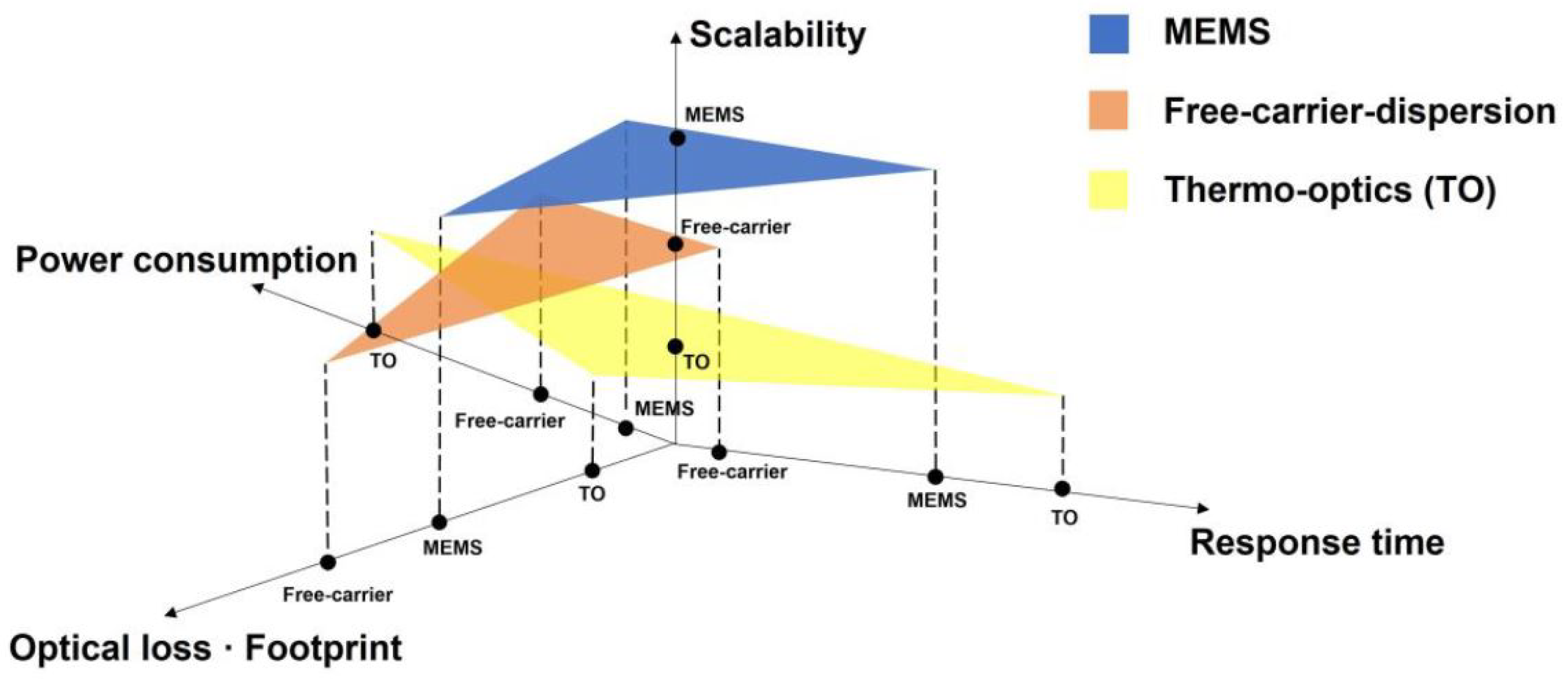
To create dense and fully operational photonic components on an SOI platform, the crossing of silicon waveguides is essential and unavoidable as system complexity grows. Simultaneously, there is a rising demand for compact device footprints. While most printed circuit boards (PCBs) for electrical circuits consist of four to eight layers, implementing efficient optical aspects for multiple layers proves challenging in the high-index contrast SOI platform. Consequently, this method is unsuitable for silicon photonic circuits due to limitations related to optical mode coupling and fabrication costs. In Ref. [128], various designs for silicon waveguide crossings, including shaped taper, multimode interference, subwavelength grating, and vertical directional coupler structures, are discussed and summarized. The FOMs of this device are the insertion losses and the waveguide crosstalk. In Ref. [129], the most optimal performance of waveguide crossings is achieved through vertical coupling with a polymer (SU-8) upper channel waveguide. FDTD simulation results indicate a crosstalk of −70 dB and an insertion loss of 0.08. An uncomplicated design [130] with low fabrication costs is demonstrated using shaped taper waveguides. The insertion losses are measured at 0.16 dB, while maintaining crosstalk levels below −40 dB.
Waveguide crossings can also serve as mode-division multiplexers, yielding satisfactory results [128].

4.2. Phase Shifter

A phase shifter is a component designed to modulate the phase of the transmission wave without altering the amplitude, which is essential for creating tunable interferometers. The simplest description involves a system with two inputs and two outputs, where the phase difference between the input signals differs from that of the output signals. Arbitrary linear optical systems can be constructed using a variety of building blocks. Chen et al. propose a review of integrated optical switches based on Mach–Zehnder Interferometers [109]. We will describe three common modulation mechanisms based on thermo-optic effects, free-carrier dispersion effects, and micro-electromechanical systems (MEMSs). The characteristics of such devices, such as optical losses, scalability, power consumption, and response time, are summarized in Figure 16.
We will use three FOMs to evaluate phase shifters: insertion losses, power consumption OR half-wave voltage length product, and response time. A summary of the characteristics of various types of grating couplers is provided Table 3.

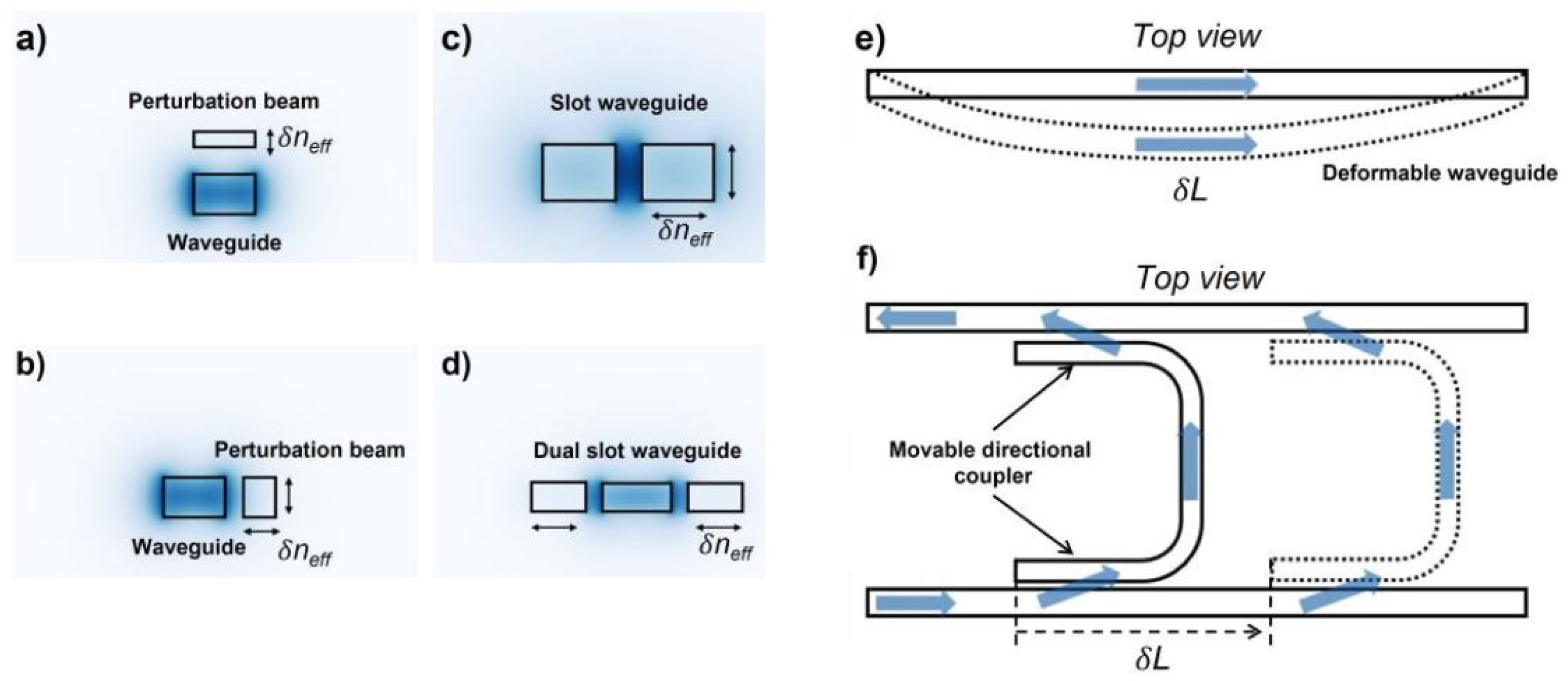
4.2.1. MEMS-Based Phase Shifter

This concept involves integrating a movable structure capable onto the chip to generate a phase shift. The implementation of such structures on SOI compels it to work with various materials and multiple layers. Additional applications of MEMS technology beyond phase shifting are reported in Ref. [132]. In the literature, three primary methods by which MEMS-based phase shifters change or adjust are described, as depicted in Figure 17. In Figure 17a,b, the adjustment occurs by perturbing the evanescent field of the optical mode in the bus waveguide, as described in [133]. In Figure 17c,d, the adjustment is achieved by directly altering the optical mode field distribution in the waveguide as a directional coupler that changes their geometric parameters [134,135,136]. Figure 17e,f depict a modulation mechanism in which the modification of the optical path length ensures low insertion losses, although the cost of a modulation speed is reduced by an order of magnitude [137].

4.2.2. Thermo-Optical Phase Shifter

The underlying concept involves locally heating the silicon waveguide to modify its refractive index, thereby altering the optical path. This type of phase shifter is widely adopted, primarily due to its ease of manufacturing, modulation efficiency, and broad bandwidth. Despite exhibiting acceptable modulation speed and insertion losses, the main critical issue remains power consumption. Various configurations are proposed in Figure 18. In the most common configuration, Figure 18a a silicon waveguide is patterned in the cladding, with a heater positioned above it. To mitigate excessive optical insertion loss, an upper cladding is grown to isolate and support the metal heater. Careful consideration of silicon width, cladding thickness, and heater type is crucial during the design process [138]. The heater con be realized from different metals and materials, such as Tungsten, TiAu, NiCr, and TiN [139], where metal structures require double layer deposition for effective adhesion (see the fabrication process in [140]).
The strategy depicted in Figure 18b enhances energy efficiency by using a separate free-standing waveguide, which helps insulate the silicon waveguide from the cladding and substrate layers [141]. There is an ongoing debate in the current literature regarding whether a device with lower consumption, with a very high time response, justifies the manufacturing complexity involved [142,143].
Figure 18c illustrates a method for reducing the vertical gap between the heater and the bus waveguide to improve power consumption and modulation speed. An optically transparent material (e.g., 2D materials such as graphene [144,145] and indium tin oxide [146]) is required to prevent significant propagation losses.
Doping silicon can also be employed as a heater, as shown in Figure 18d,e, which exhibit an adequate balance between the FOMs [147,148].
More intricate and unconventional structures aimed at minimizing chip heating and enhancing the effective phase shifter length have been proposed recently. One example of a simpler structure involves waveguides following a spiral path beneath a heater [149]. Miller et al. [150] introduced additional complex structures, such as multiple directional couplers acting as mirrors. A multi-layer thermal phase shifter made of emerging phase-change materials (Sb2Se3), a Ti/Au heater, and graphene structures can be effective in a ring resonator thanks to their compact dimensions [151] with a length as small as 6 μm.

4.2.3. Free-Carrier-Depletion-Based Phase Shifter

Phase shifters that take advantage of the free-carrier dispersion are preferred in telecommunications and data center applications because of their rapid modulation capability and minimal energy consumption. The principle is to modify the concentration of charge carriers within the waveguide to alter the refractive index. This is accomplished through p-n doping junctions, which, in the absence of applied voltages, do not change the optical path. The cross-section is segmented into regions with variable doping concentrations. In region (i), the semiconductor is intrinsic (pure Si), with ’p’ representing free holes and ’n’ representing free electrons. The symbols ’+’ and ’++’ denote different levels of doping concentration, usually from 10 13 cm 3 to 10 18 cm 3 . The distribution of the doping area and the doping concentrations are crucial parameters influencing both the modulation efficiency (Vπ·Lπ), where Vπ and Lπ are, respectively, the applied voltage and the device length needed to have a phase shift of π , and the propagation loss of the doped waveguide. Various designs are presented in Figure 19 to achieve the depletion zone.
Figure 19. Various structures of free-carrier-depletion-based phase shifters. (a) Phase shifter with offset carrier doping [152,153], (b) PIPIN phase shifters [154], (c) phase shifter with counter doping at corners [155], (d) phase shifter with epitaxy fabrication [156], (e) phase shifters with substrate removement [157], (f) interleaved structure phase shifter [158], (g) zig-zag structure phase shifter [159]. Image reproduced by [131].
Photonics 11 00494 g019
Table 3. Overview of different phase shifters; * modulation efficiency (Vπ·Lπ) for MEMSs and depletion (PN Reverse Bias Voltage) power consumption for thermal phase shifters.
Shifter TypeEfficiency * (V · mm) and Consumption * (mW)Modulation Speed (MHz)Insertion Loss (dB)
MEMS evanescent field perturbation [133]0.5350.5030.33 dB
MEMS optical mode
modification [135]0.020.040.26 dB
MEMS opt. path length adjustment [137]750.1390.1 dB
TPS conventional TiN heater [147]21.4 mW0.18<0.01 dB
TPS Doped Silicon [147]22.8 mW0.45<0.01 dB
TPS 2D layer ITO [146]10 mW0.19<0.01 dB
Conventional TPS with air trench [143]1.7 mW0.0100.1 dB
TPS spiral waveguide [149]3 mW0.0390.9 dB
Standard PN junction [153]∼0.8 V · mm (3 V)12 × 1031.2 dB
Junction PIPIN [154]35 V · mm (0 V)42 × 1032.5 dB
Corner doping
concentration [155]26.7 V · mm (−6 V)8.9 × 1034.5 dB
Grown vertical junction diodes [156]7.4 V · mm (1 V)48 × 1033.8 dB
Interleaved PN [159]1.9 V · mm (1 V)6.8 × 10³∼2 dB

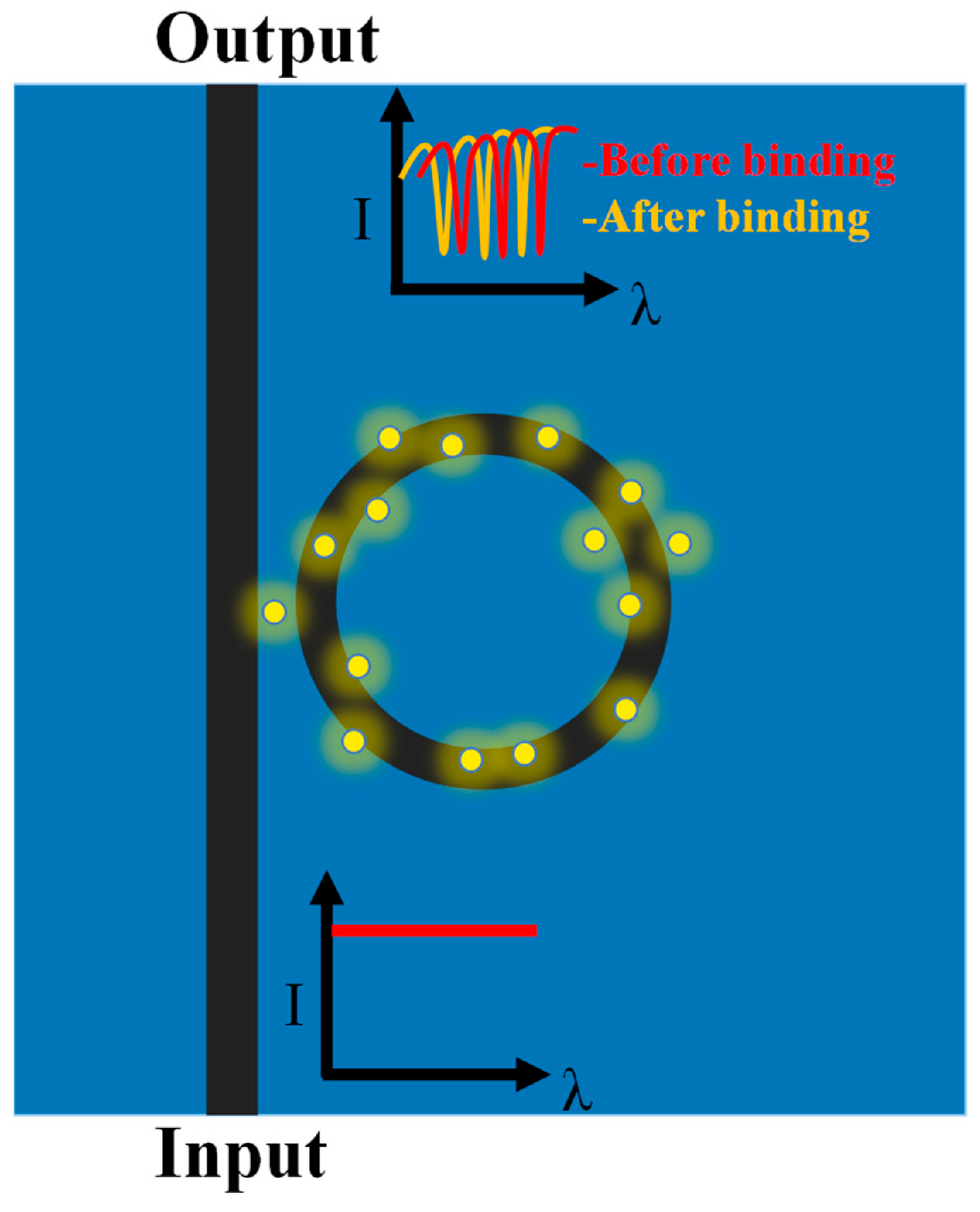
4.3. Ring Resonators

A ring resonator (RR) is a passive component typically composed of a ring-shaped waveguide made from a high-refractive-index material, such as silicon, which is connected to a bus waveguide. The RR is specifically designed to exhibit a resonant frequency determined by its dimensions and refractive index (RI). When light is introduced into the waveguide, it circulates within the ring and interferes with itself. The resonant frequency of the ring corresponds to the frequency at which the light waves combine constructively, resulting in a significant signal detectable by an external photodetector. Changes in the refractive index of the surrounding medium can influence the resonant frequency of the ring, leading to a shift in the output signal.
Ring resonators are indispensable optical devices in photonics and telecommunications. Their functionality relies on connectivity, which is often established through evanescent coupling with a nearby bus waveguide. RRs integrated into a bus waveguide create dips in the transmission spectrum, serving as spectrum filters applicable in optical communication, especially in wavelength division multiplexing [160]. While the resonance dips offer high sensitivity, providing advantages for sensing and tuning, they may present challenges for filter stability.
RRs serve as narrowband filters and are crucial in optical communication systems like WDM and optical add-drop multiplexing. Additionally, they operate as optical modulators, facilitating the modulation of transmitted light intensity for applications such as optical data transmission. RRs also function as sensors and are capable of detecting variations in the refractive index for chemical, temperature, pressure [161], and biological sensing. In the realm of nonlinear optics, RRs induce nonlinear effects, enabling applications such as frequency doubling and entangled photon generation, as shown in Figure 20. Consequently, RRs play a pivotal role in quantum computing.
In 2023, Kazanskiy et al. [162] explored various applications, including biomedical sensing, environmental monitoring, and chemical analysis, focusing solely on RRs in the SOI platform. However, it is worth noting that the same structure can also be implemented on plasmonic and polymer platforms. One key parameter of the ring resonator is its sensitivity, which is typically measured in terms of Δ λ RIU RIU: refractive index unit). On the SOI platform, the sensitivity of μ -RR-based sensors is less than 100 nm RIU . However, employing subwavelength grating RRs enables the attainment of a sensitivity as high as 672.8 nm RIU .
Similarly to other resonators, the quality factor (Q) is another critical parameter. It quantifies the ratio of the energy stored in the resonator to the energy lost per resonant cycle. Typical values of Q for SOI devices fall within the range of 10 3 to 10 4 . For the limit of weakly damped oscillations (high Q values), Q is the ratio of the resonance frequency ν 0 and the full width at half-maximum (FWHM) bandwidth δ ν of the resonance [163]:
Q = ν 0 δ ν
RRs are presented in the literature in relation to their applications. In 2022, Kumari et al. proposed a Silicon-On-Insulator waveguide-technology-based 1 × 2 integrated photonic beamformer for a 28 GHz signal with a device with a 30 μm radius, 425 nm RIU [164].
Among semiconductor-based RR devices tailored for gas detection, the study in [165] stands out. In the NIR spectrum, the presence and pressure of acetylene gas prompt oscillations in the resonance wavelength, coupled with marginal variations in the refractive index of up to 10 4 . Benefitting from the slot waveguide design, the device shows a sensitivity of 490 nm RIU and a high Q factor of 5000.
Ring resonator biosensors detect minute changes in chemical liquid composition [166]. Using standard ring resonators with porous silicon waveguides, two radii (10 and 25 μm) are tested through exposure to varied saltwater solutions, gauging their overall sensitivity. Active characterization of porous silicon rings shows a bulk detection sensitivity of about 380 nm RIU ( Q = 10 4 ) and a surface sensitivity of roughly 4 pm/nM.is revision.
In the subwavelength grating ring resonator, both the ring and the straight waveguide are fabricated using discrete small bricks. Kundal et al. [167] propose a radius of 5 μm yielding exceptional sensitivity, documented in the literature at 1012 nm RIU and Q = 1012.
A very recent review produced in 2024 by Saha et al. [168] provides a comprehensive overview of four key filter architectures—microring resonators, waveguide Bragg gratings, Mach–Zehnder interferometers, and arrayed waveguide gratings—offering insights into their basics, simulation tools, and applications. By summarizing these architectures concisely, the review sheds light on the importance and future trends of silicon photonic filters from both research and commercialization perspectives.

5. Conclusions and Perspectives

Integrated photonics has emerged as a pivotal force in advancing quantum devices and facilitating their global commercialization. The establishment of research hubs worldwide has cultivated expertise in photonic integration, forming a robust foundation for progress. Concerted efforts are now essential to fortify PICs and drive further advancements.
In the realm of modern computing, photonics and optical fibers play indispensable roles in high-speed data processing and transport. Silicon photonics technology offers a promising avenue to significantly reduce the cost, complexity, and power consumption of photonic connections.
Our aim in this review has been to provide a comprehensive yet concise list of optical components suitable for the Silicon-On-Insulator (SOI) platform. By focusing on both fabrication considerations and the specific characteristics of each component, we strive to contribute to the advancement of PIC technologies. We believe that this compilation will prove valuable to researchers and engineers working in the field, aiding in the development of more efficient and robust photonic integrated circuits for various applications.

Author Contributions

All authors contributed to this work: writing—original draft preparation, D.P.; writing—review and editing, all authors. All authors have read and agreed to the published version of the manuscript.

Funding

This work was funded by INFN through the CSN5 QUANTEP project.

Acknowledgments

V.B. (Vittorio Bellani), G.D.G., A.F., R.G., C.L., E.P., P.P. (Paolo Piergentili), V.R., C.R., and F.S. (Franco Spinella) acknowledge the support of the PNRR MUR project PE0000023-NQSTI (Italy).

Conflicts of Interest

The authors declare no conflicts of interest.

References

  1. Lipson, M. The revolution of silicon photonics. Nat. Mater. 2022, 21, 974–975. [Google Scholar] [CrossRef]
  2. Shahbaz, M.; Butt, M.A.; Piramidowicz, R. A Concise Review of the Progress in Photonic Sensing Devices. Photonics 2023, 10, 698. [Google Scholar] [CrossRef]
  3. Shekhar, S.; Bogaerts, W.; Chrostowski, L.; Bowers, J.E.; Hochberg, M.; Soref, R.; Shastri, B.J. Roadmapping the next generation of silicon photonics. Nat. Commun. 2024, 15, 751. [Google Scholar] [CrossRef]
  4. Pelucchi, E.; Fagas, G.; Aharonovich, I.; Englund, D.; Figueroa, E.; Gong, Q.; Hannes, H.; Liu, J.; Lu, C.Y.; Matsuda, N.; et al. The potential and global outlook of integrated photonics for quantum technologies. Nat. Rev. Phys. 2022, 4, 194–208. [Google Scholar] [CrossRef]
  5. Piergentili, P.; Amanti, F.; Andrini, G.; Armani, F.; Bellani, V.; Bonaiuto, V.; Cammarata, S.; Campostrini, M.; Cornia, S.; Dao, T.H.; et al. Quantum Information with Integrated Photonics. Appl. Sci. 2023, 14, 387. [Google Scholar] [CrossRef]
  6. Siew, S.Y.; Li, B.; Gao, F.; Zheng, H.Y.; Zhang, W.; Guo, P.; Xie, S.W.; Song, A.; Dong, B.; Luo, L.W.; et al. Review of silicon photonics technology and platform development. J. Light. Technol. 2021, 39, 4374–4389. [Google Scholar] [CrossRef]
  7. Andrini, G.; Amanti, F.; Armani, F.; Bellani, V.; Bonaiuto, V.; Cammarata, S.; Campostrini, M.; Dao, T.H.; De Matteis, F.; Demontis, V.; et al. Solid-State Color Centers for Single-Photon Generation. Photonics 2024, 11, 188. [Google Scholar] [CrossRef]
  8. Ceccarelli, F.; Acconcia, G.; Gulinatti, A.; Ghioni, M.; Rech, I.; Osellame, R. Recent advances and future perspectives of single-photon avalanche diodes for quantum photonics applications. Adv. Quantum Technol. 2021, 4, 2000102. [Google Scholar] [CrossRef]
  9. Xiang, C.; Bowers, S.M.; Bjorlin, A.; Blum, R.; Bowers, J.E. Perspective on the future of silicon photonics and electronics. Appl. Phys. Lett. 2021, 118, 220501. [Google Scholar]
  10. Mu, X.; Wu, S.; Cheng, L.; Fu, H. Edge couplers in silicon photonic integrated circuits: A review. Appl. Sci. 2020, 10, 1538. [Google Scholar] [CrossRef]
  11. Cheng, L.; Mao, S.; Li, Z.; Han, Y.; Fu, H. Grating couplers on silicon photonics: Design principles, emerging trends and practical issues. Micromachines 2020, 11, 666. [Google Scholar] [CrossRef]
  12. Marchetti, R.; Lacava, C.; Carroll, L.; Gradkowski, K.; Minzioni, P. Coupling strategies for silicon photonics integrated chips. Photonics Res. 2019, 7, 201–239. [Google Scholar] [CrossRef]
  13. Carroll, L.; Lee, J.S.; Scarcella, C.; Gradkowski, K.; Duperron, M.; Lu, H.; Zhao, Y.; Eason, C.; Morrissey, P.; Rensing, M.; et al. Photonic packaging: Transforming silicon photonic integrated circuits into photonic devices. Appl. Sci. 2016, 6, 426. [Google Scholar] [CrossRef]
  14. Cardenas, J.; Luke, K.; Luo, L.; Poitras, C.; Morton, P.; Lipson, M. High coupling efficiency etched facet tapers in silicon. In Proceedings of the 2012 Conference on Lasers and Electro-Optics, San Jose, CA, USA, 6–11 May 2012. [Google Scholar]
  15. Chuang, S. Physics of Photonic Devices, 2nd ed.; John Wiley & Sons, Inc.: Hoboken, NJ, USA, 2009; pp. 273–279. [Google Scholar]
  16. Chrostowski, L.; Hochberg, M. Silicon Photonics Design: From Devices to Systems, 1st ed.; Cambridge University Press: Cambridge, UK, 2015; pp. 10–14. [Google Scholar]
  17. Dong, P.; Preble, S.F.; Robinson, J.T.; Manipatruni, S.; Lipson, M. Inducing photonic transitions between discrete modes in a silicon optical microcavity. Phys. Rev. Lett. 2008, 100, 033904. [Google Scholar] [CrossRef]
  18. Stern, B.; Zhu, X.; Chen, C.P.; Tzuang, L.D.; Cardenas, J.; Bergman, K.; Lipson, M. On-chip mode-division multiplexing switch. Optica 2015, 2, 530–535. [Google Scholar] [CrossRef]
  19. He, Y.; Zhang, Y.; Zhu, Q.; An, S.; Cao, R.; Guo, X.; Qiu, C.; Su, Y. Silicon high-order mode (de) multiplexer on single polarization. J. Light. Technol. 2018, 36, 5746–5753. [Google Scholar] [CrossRef]
  20. Fu, Y.; Ye, T.; Tang, W.; Chu, T. Efficient adiabatic silicon-on-insulator waveguide taper. Photonics Res. 2014, 2, 41–44. [Google Scholar] [CrossRef]
  21. Seok, T.; Quack, N.; Han, S.; Muller, R.; Wu, M. Large-scale broadband digital silicon photonic switches with vertical adiabatic couplers. Optica 2016, 3, 64–70. [Google Scholar] [CrossRef]
  22. Suchoski, P.; Ramaswamy, R. Design of single-mode step-tapered waveguide sections. IEEE J. Sel. Top. Quant. 1987, 23, 205–211. [Google Scholar] [CrossRef]
  23. Wang, J.; Qi, M.; Xuan, Y.; Huang, H.; Li, Y.; Li, M.; Chen, X.; Jia, Q.; Sheng, Z.; Wu, A.; et al. Proposal for fabrication-tolerant SOI polarization splitter-rotator based on cascaded MMI couplers and an assisted bi-level taper. Opt. Express 2014, 22, 27869–27879. [Google Scholar] [CrossRef]
  24. Hettrick, S.; Wang, J.; Li, C.; Wilkinson, J.; Shepherd, D. An experimental comparison of linear and parabolic tapered waveguide lasers and a demonstration of broad-stripe diode pumping. J. Light. Technol. 2004, 22, 845–849. [Google Scholar] [CrossRef]
  25. Ren, G.; Chen, S.; Cheng, Y.; Zhai, Y. Study on inverse taper based mode transformer for low loss coupling between silicon wire waveguide and lensed fiber. Opt. Commun. 2011, 284, 4782–4788. [Google Scholar] [CrossRef]
  26. Snyder, A.; Love, J. Optical Waveguide Theory; Springer Science & Business Media: New York, NY, USA, 2012; pp. 238–280. [Google Scholar]
  27. Liu, Y.; Yu, J. Low-loss coupler between fiber and waveguide based on silicon-on-insulator slot waveguides. Appl. Opt. 2007, 46, 7858–7861. [Google Scholar] [CrossRef]
  28. Tu, X.; Fu, H.; Geng, D. Y-branch edge coupler between cleaved single mode fiber and nano-scale waveguide on silicon-on-insulator platform. In Proceedings of the 2014 Asia Communications and Photonics Conference, Shanghai, China, 11–14 November 2014. [Google Scholar]
  29. Mu, X.; Wu, S.; Cheng, L.; Tu, X.; Fu, H. High-performance silicon nitride fork-shape edge coupler. In Proceedings of the 2019 Frontiers in Optics, Washington, DC, USA, 15–19 September 2019. [Google Scholar]
  30. Tu, Y.; Fu, P.; Huang, D. High-efficiency ultra-broadband multi-tip edge couplers for integration of distributed feedback laser with silicon-on-insulator waveguide. IEEE Photonics J. 2019, 11, 1–13. [Google Scholar] [CrossRef]
  31. Wang, J.; Xuan, Y.; Lee, C.; Niu, B.; Liu, L.; Liu, G.; Qi, M. Low-loss and misalignment-tolerant fiber-to-chip edge coupler based on double-tip inverse tapers. In Proceedings of the 2016 Optical Fiber Communications Conference and Exhibition (OFC), Anaheim, CA, USA, 20–24 March 2016. [Google Scholar]
  32. Hatori, N.; Urino, Y.; Shimizu, T.; Okano, M.; Yamamoto, T.; Mori, M.; Nakamura, T.; Arakawa, Y. Quantum dot laser for a light source of an athermal silicon optical interposer. Photonics 2015, 2, 355–364. [Google Scholar] [CrossRef]
  33. Itoh, K.; Kuno, Y.; Hayashi, Y.; Suzuki, J.; Hojo, N.; Amemiya, T.; Nishiyama, N.; Arai, S. Crystalline/Amorphous Si Integrated Optical Couplers for 2D/3D Interconnection. IEEE J. Sel. Top. Quantum Electron. 2016, 22, 255–263. [Google Scholar] [CrossRef]
  34. Tu, X.; Dumais, P.; Li, M.; Goodwill, D.; Fu, H.; Geng, D.; Bernier, E. Low polarization-dependent-loss silicon photonic trident edge coupler fabricated by 248 nm optical lithography. In Proceedings of the Asia Communications and Photonics Conference, Hong Kong, 19–23 November 2015; Optica Publishing Group: Washington, DC, USA; p. AS4B-3. [Google Scholar]
  35. Cheben, P.; Bock, P.J.; Schmid, J.H.; Lapointe, J.; Janz, S.; Xu, D.X.; Densmore, A.; Delâge, A.; Lamontagne, B.; Hall, T.J. Refractive index engineering with subwavelength gratings for efficient microphotonic couplers and planar waveguide multiplexers. Opt. Lett. 2010, 35, 2526–2528. [Google Scholar] [CrossRef]
  36. Cheben, P.; Schmid, J.H.; Wang, S.; Xu, D.X.; Vachon, M.; Janz, S.; Lapointe, J.; Painchaud, Y.; Picard, M.J. Broadband polarization independent nanophotonic coupler for silicon waveguides with ultra-high efficiency. Opt. Express 2015, 23, 22553–22563. [Google Scholar] [CrossRef]
  37. Donzella, V.; Sherwali, A.; Flueckiger, J.; Fard, S.T.; Grist, S.M.; Chrostowski, L. Sub-wavelength grating components for integrated optics applications on SOI chips. Opt. Express 2014, 22, 21037–21050. [Google Scholar] [CrossRef]
  38. Cheben, P.; Xu, D.; Janz, S.; Densmore, A. Subwavelength waveguide grating for mode conversion and light coupling in integrated optics. Opt. Express 2006, 14, 4695–4702. [Google Scholar] [CrossRef]
  39. Voigt, K.; Brulis, V.; Petermann, K.; Zimmermann, L. Study of backend waveguide arrays for adiabatic coupling to Si waveguides. In Proceedings of the 2017 IEEE 14th International Conference on Group IV Photonics (GFP), Berlin, Germany, 23–25 August 2017; IEEE: New York, NY, USA, 2017; pp. 143–144. [Google Scholar]
  40. Picard, M.J.; Latrasse, C.; Larouche, C.; Painchaud, Y.; Poulin, M.; Pelletier, F.; Guy, M. CMOS-compatible spot-size converter for optical fiber to sub-um silicon waveguide coupling with low-loss low-wavelength dependence and high tolerance to misalignment. In Proceedings of the Silicon Photonics XI. SPIE, San Francisco, CA, USA, 14 March 2016; Volume 9752, pp. 132–138. [Google Scholar]
  41. Sisto, M.M.; Fisette, B.; Paultre, J.E.; Paquet, A.; Desroches, Y. Novel spot size converter for coupling standard single mode fibers to SOI waveguides. In Proceedings of the Silicon Photonics XI. SPIE, San Francisco, CA, USA, 14 March 2016; Volume 9752, pp. 199–213. [Google Scholar]
  42. Doylend, J.K.; Knights, A.P. Design and Simulation of an Integrated Fiber-to-Chip Coupler for Silicon-on-Insulator Waveguides. IEEE J. Sel. Top. Quantum Electron. 2006, 12, 1363–1370. [Google Scholar] [CrossRef]
  43. Kruse, K.; Middlebrook, C.T. Polymer taper bridge for silicon waveguide to single mode waveguide coupling. Opt. Commun. 2016, 362, 87–95. [Google Scholar] [CrossRef]
  44. Dewanjee, A.; Caspers, J.N.; Aitchison, J.S.; Mojahedi, M. Demonstration of a compact bilayer inverse taper coupler for Si-photonics with enhanced polarization insensitivity. Opt. Express 2016, 24, 28194–28203. [Google Scholar] [CrossRef]
  45. Khilo, A.; Popović, M.A.; Araghchini, M.; Kärtner, F.X. Efficient planar fiber-to-chip coupler based on two-stage adiabatic evolution. Opt. Express 2010, 18, 15790–15806. [Google Scholar] [CrossRef]
  46. Park, H.; Kim, S.; Park, J.; Joo, J.; Kim, G. A fiber-to-chip coupler based on Si/SiON cascaded tapers for Si photonic chips. Opt. Express 2013, 21, 29313–29319. [Google Scholar] [CrossRef]
  47. Fang, Q.; Song, J.; Luo, X.; Tu, X.; Jia, L.; Yu, M.; Lo, G. Low Loss Fiber-to-Waveguide Converter With a 3-D Functional Taper for Silicon Photonics. IEEE Photonics Technol. Lett. 2016, 28, 2533–2536. [Google Scholar] [CrossRef]
  48. Lee, J.M.; Kim, D.J.; Ahn, H.; Park, S.H.; Kim, G. Temperature Dependence of Silicon Nanophotonic Ring Resonator With a Polymeric Overlayer. J. Light. Technol. 2007, 25, 2236–2243. [Google Scholar] [CrossRef]
  49. Raghunathan, V.; Yagüe, J.L.; Xu, J.; Michel, J.; Gleason, K.K.; Kimerling, L.C. Co-polymer clad design for high performance athermal photonic circuits. Opt. Express 2012, 20, 20808–20813. [Google Scholar] [CrossRef]
  50. Pu, M.; Liu, L.; Ou, H.; Yvind, K.; Hvam, J.M. Ultra-low-loss inverted taper coupler for silicon-on-insulator ridge waveguide. Opt. Commun. 2010, 283, 3678–3682. [Google Scholar] [CrossRef]
  51. Ku, K.N.; Lee, M.C.M. Wide-band optical mode converters for coupling between fibers and silicon photonic wires with large misalignment tolerance. J. Light. Technol. 2013, 31, 1616–1620. [Google Scholar] [CrossRef]
  52. Nguyen, M.H.; Chang, C.J.; Lee, M.C.; Tseng, F.G. SU8 3D prisms with ultra small inclined angle for low-insertion-loss fiber/waveguide interconnection. Opt. Express 2011, 19, 18956–18964. [Google Scholar] [CrossRef] [PubMed]
  53. Harke, A.; Lipka, T.; Amthor, J.; Horn, O.; Krause, M.; Muller, J. Amorphous Silicon 3-D Tapers for Si Photonic Wires Fabricated With Shadow Masks. IEEE Photonics Technol. Lett. 2008, 20, 1452–1454. [Google Scholar] [CrossRef]
  54. Jia, L.; Song, J.; Liow, T.Y.; Luo, X.; Tu, X.; Fang, Q.; Koh, S.C.; Yu, M.; Lo, G. Mode size converter between high-index-contrast waveguide and cleaved single mode fiber using SiON as intermediate material. Opt. Express 2014, 22, 23652–23660. [Google Scholar] [CrossRef] [PubMed]
  55. Maegami, Y.; Takei, R.; Omoda, E.; Amano, T.; Okano, M.; Mori, M.; Kamei, T.; Sakakibara, Y. Spot-size converter with a SiO2 spacer layer between tapered Si and SiON waveguides for fiber-to-chip coupling. Opt. Express 2015, 23, 21287–21295. [Google Scholar] [CrossRef] [PubMed]
  56. Zhang, Y.; Ling, Y.C.; Zhang, Y.; Shang, K.; Yoo, S.J.B. High-Density Wafer-Scale 3-D Silicon-Photonic Integrated Circuits. IEEE J. Sel. Top. Quantum Electron. 2018, 24, 1–10. [Google Scholar] [CrossRef]
  57. Zhang, W.; Ebert, M.; Reynolds, J.; Chen, B.; Yan, X.; Du, H.; Banakar, M.; Tran, D.; Littlejohns, C.; Reed, G.; et al. Buried 3D spot-size converters for silicon photonics. Optica 2021, 8, 1102–1108. [Google Scholar] [CrossRef]
  58. Li, X.; Yu, S.; Gui, C. Fiber-to-Chip Three-Dimensional Silicon-on-Insulator Edge Couplers with High Efficiency and Tolerance. Micromachines 2023, 14, 1500. [Google Scholar] [CrossRef] [PubMed]
  59. Zhao, J.; Wang, Z.; Ye, N.; Pang, F.; Song, Y. The low-loss spot size converter for alignment with cleaved single mode fiber. Appl. Sci. 2023, 13, 8157. [Google Scholar] [CrossRef]
  60. Brunetti, G.; Heuvink, R.; Schreuder, E.; Armenise, M.; Ciminelli, C. Silicon Nitride Spot Size Converter With Very Low-Loss over the C-Band. IEEE Photonics Technol. Lett. 2023, 35, 1215–1218. [Google Scholar] [CrossRef]
  61. Fang, Q.; Liow, T.Y.; Song, J.F.; Tan, C.W.; Yu, M.B.; Lo, G.Q.; Kwong, D.L. Suspended optical fiber-to-waveguide mode size converter for silicon photonics. Opt. Express 2010, 18, 7763–7769. [Google Scholar] [CrossRef]
  62. Wood, M.; Sun, P.; Reano, R.M. Compact cantilever couplers for low-loss fiber coupling to silicon photonic integrated circuits. Opt. Express 2012, 20, 164–172. [Google Scholar] [CrossRef] [PubMed]
  63. Nambiar, S.; Sethi, P.; Selvaraja, S.K. Grating-assisted fiber to chip coupling for SOI photonic circuits. Appl. Sci. 2018, 8, 1142. [Google Scholar] [CrossRef]
  64. Mahajan, R.; Li, X.; Fryman, J.; Zhang, Z.; Nekkanty, S.; Tadayon, P.; Jaussi, J.; Shumarayev, S.; Agrawal, A.; Jadhav, S.; et al. Co-packaged photonics for high performance computing: Status, challenges and opportunities. J. Light. Technol. 2021, 40, 379–392. [Google Scholar] [CrossRef]
  65. Subbaraman, H.; Xu, X.; Hosseini, A.; Zhang, X.; Zhang, Y.; Kwong, D.; Chen, R.T. Recent advances in silicon-based passive and active optical interconnects. Opt. Express 2015, 23, 2487–2511. [Google Scholar] [CrossRef]
  66. Kopp, C.; Bernabe, S.; Bakir, B.B.; Fedeli, J.M.; Orobtchouk, R.; Schrank, F.; Porte, H.; Zimmermann, L.; Tekin, T. Silicon photonic circuits: On-CMOS integration, fiber optical coupling, and packaging. IEEE J. Sel. Top. Quantum Electron. 2010, 17, 498–509. [Google Scholar] [CrossRef]
  67. Snyder, B.; O’Brien, P. Packaging process for grating-coupled silicon photonic waveguides using angle-polished fibers. IEEE Trans. Compon. Packag. Manuf. Technol. 2013, 3, 954–959. [Google Scholar] [CrossRef]
  68. Karnick, D.; Skwierawski, P.; Schneider, M.; Eisenblätter, L.; Weber, M. Optical links for detector instrumentation: On-detector multi-wavelength silicon photonic transmitters. J. Instrum. 2017, 12, C03078. [Google Scholar] [CrossRef]
  69. Zhou, X.; Tsang, H.K. High efficiency multimode waveguide grating coupler for few-mode fibers. IEEE Photonics J. 2022, 14, 1–5. [Google Scholar] [CrossRef]
  70. Wu, Y.; Wu, Y.; Xu, J.; Wang, X.; Wu, Y.; Chen, Y.; Li, J.; Xu, K. An Efficient Silicon Grating Coupler for a 2 μm Waveband Based on a Polysilicon Overlay. Photonics 2023, 10, 952. [Google Scholar] [CrossRef]
  71. Vermeer, M.L.; Alhareeb, N.K.; Trieu, H.K.; Lipka, T. Fabrication of distributed Bragg reflectors to reduce coupling losses of photonic circuits. In Proceedings of the Mikro-Nano-Integration; 9. GMM-Workshop, Aachen, Germany, 21–22 November 2022; pp. 1–4. [Google Scholar]
  72. Hoppe, N.; Zaoui, W.S.; Rathgeber, L.; Wang, Y.; Klenk, R.H.; Vogel, W.; Kaschel, M.; Portalupi, S.L.; Burghartz, J.; Berroth, M. Ultra-efficient silicon-on-insulator grating couplers with backside metal mirrors. IEEE J. Sel. Top. Quantum Electron. 2019, 26, 1–6. [Google Scholar] [CrossRef]
  73. Sharma, T.; Kwon, H.; Park, J.; Han, S.; Son, G.; Jung, Y.; Yu, K. Coupling performance enhancement using SOI grating coupler design. Opt. Commun. 2018, 427, 452–456. [Google Scholar] [CrossRef]
  74. He, L.; Liu, Y.; Galland, C.; Lim, A.E.J.; Lo, G.Q.; Baehr-Jones, T.; Hochberg, M. A High-Efficiency Nonuniform Grating Coupler Realized With 248-nm Optical Lithography. IEEE Photonics Technol. Lett. 2013, 25, 1358–1361. [Google Scholar] [CrossRef]
  75. Benedikovic, D.; Alonso-Ramos, C.; Pérez-Galacho, D.; Guerber, S.; Vakarin, V.; Marcaud, G.; Le Roux, X.; Cassan, E.; Marris-Morini, D.; Cheben, P.; et al. L-shaped fiber-chip grating couplers with high directionality and low reflectivity fabricated with deep-UV lithography. Opt. Lett. 2017, 42, 3439–3442. [Google Scholar] [CrossRef]
  76. Zhao, Z.; Fan, S. Design Principles of Apodized Grating Couplers. J. Light. Technol. 2020, 38, 4435–4446. [Google Scholar] [CrossRef]
  77. Hansen, S.E.; Arregui, G.; Babar, A.N.; Albrechtsen, M.; Lahijani, B.V.; Christiansen, R.E.; Stobbe, S. Efficient low-reflection fully etched vertical free-space grating couplers for suspended silicon photonics. Opt. Express 2023, 31, 17424–17436. [Google Scholar] [CrossRef]
  78. Li, S.; Zhou, C.; Cao, H.; Wu, J. Simple design of slanted grating with simplified modal method. Opt. Lett. 2014, 39, 781–784. [Google Scholar] [CrossRef]
  79. Schrauwen, J.; Van Laere, F.; Van Thourhout, D.; Baets, R. Focused-Ion-Beam Fabrication of Slanted Grating Couplers in Silicon-on-Insulator Waveguides. IEEE Photonics Technol. Lett. 2007, 19, 816–818. [Google Scholar] [CrossRef]
  80. Watanabe, T.; Fedoryshyn, Y.; Leuthold, J. 2-D Grating Couplers for Vertical Fiber Coupling in Two Polarizations. IEEE Photonics J. 2019, 11, 1–9. [Google Scholar] [CrossRef]
  81. Lin, C.C.; Lu, Y.C.; Liu, Y.H.; Wang, L.; Na, N. Design of a Completely Vertical, Polarization-Independent Two-Dimensional Grating Coupler with High Coupling Efficiency. Sensors 2023, 23, 4662. [Google Scholar] [CrossRef]
  82. Kumar, P.; Mishra, A.; Shivaleela, E.; Srinivas, T. Inverse Design of SOI based broadband Grating Coupler. In Proceedings of the 2022 IEEE Research and Applications of Photonics in Defense Conference (RAPID), Miramar Beach, FL, USA, 12–14 September 2022; IEEE: New York, NY, USA, 2022; pp. 1–2. [Google Scholar]
  83. Cheng, G.; Yi, Q.; Xu, F.; Yang, M.; Yan, Z.; Li, Q.; Zou, Y.; Yu, Y.; Shen, L. Efficient 1.55 and 2 μm Dual-Band SOI Grating Coupler for Light Coupling and On-Chip Wavelength Division (De) multiplexing. Adv. Photonics Res. 2023, 4, 2200149. [Google Scholar] [CrossRef]
  84. Xu, Y.; Tian, Z.; Meng, X.; Chai, Z. Methods and applications of on-chip beam splitting: A review. Front. Phys. 2022, 10, 985208. [Google Scholar] [CrossRef]
  85. Yang, N.; Xiao, J. A compact silicon-based polarization-independent power splitter using a three-guide directional coupler with subwavelength gratings. Opt. Commun. 2020, 459, 125095. [Google Scholar] [CrossRef]
  86. Zhang, Y.; Yang, S.; Lim, A.E.J.; Lo, G.Q.; Galland, C.; Baehr-Jones, T.; Hochberg, M. A compact and low loss Y-junction for submicron silicon waveguide. Opt. Express 2013, 21, 1310–1316. [Google Scholar] [CrossRef] [PubMed]
  87. Zhang, Y.; Hu, X.; Chen, D.; Wang, L.; Li, M.; Feng, P.; Xiao, X.; Yu, S. Ultra-broadband, Low Loss and Ultra-Compact 3dB Power Splitter Based On Y-Branch With Step Waveguide. In Proceedings of the 2019 24th OptoElectronics and Communications Conference (OECC) and 2019 International Conference on Photonics in Switching and Computing (PSC), Fukuoka, Japan, 7–11 July 2019; IEEE: New York, NY, USA, 2019; pp. 1–3. [Google Scholar]
  88. Han, L.; Kuo, B.P.P.; Alic, N.; Radic, S. Ultra-broadband multimode 3dB optical power splitter using an adiabatic coupler and a Y-branch. Opt. Express 2018, 26, 14800–14809. [Google Scholar] [CrossRef] [PubMed]
  89. Pendam, N.; Vardhani, C. Design, simulation & optimization of 3D low-loss asymmetrical Y-branch optical power splitter on SOI platform. In Proceedings of the 2016 International Conference on Electrical, Electronics, and Optimization Techniques (ICEEOT), Chennai, India, 3–5 March 2016; IEEE: New York, NY, USA, 2016; pp. 755–757. [Google Scholar]
  90. Ozcan, C.; Mojahedi, M.; Aitchison, J.S. Short, broadband, and polarization-insensitive adiabatic Y-junction power splitters. Opt. Lett. 2023, 48, 4901–4904. [Google Scholar] [CrossRef] [PubMed]
  91. Ni, B.; Xiao, J. Ultracompact and broadband silicon-based TE-pass 1 × 2 power splitter using subwavelength grating couplers and hybrid plasmonic gratings. Opt. Express 2018, 26, 33942–33955. [Google Scholar] [CrossRef] [PubMed]
  92. Huang, G.; Park, T.H.; Oh, M.C. Broadband integrated optic polarization splitters by incorporating polarization mode extracting waveguide. Sci. Rep. 2017, 7, 4789. [Google Scholar] [CrossRef]
  93. Sun, Y.; Zhang, L.; Xia, H.; Cao, S.; Wang, L.; Yang, S.; Wu, Y.; Tai, R. Integrated silicon metasurface polarization beam splitter on a standard SOI substrate. Optik 2021, 227, 166096. [Google Scholar] [CrossRef]
  94. Liao, J.; Tian, Y.; Yang, Z.; Xu, H.; Tang, C.; Wang, Y.; Zhang, X.; Kang, Z. Inverse design of highly efficient and broadband mode splitter on SOI platform. Chin. Opt. Lett. 2024, 22, 011302. [Google Scholar] [CrossRef]
  95. Lv, D.; Wu, L.; Liu, C.; Li, A.; Wang, R.; Wu, A. Broadband and Low-Loss Silicon Photonic Directional Coupler for Signal Power Tapping on the 3 μm SOI Waveguide Platform. Photonics 2023, 10, 776. [Google Scholar] [CrossRef]
  96. Paredes, B.; Mohammed, Z.; Villegas, J.; Rasras, M. Dual-band (O & C-bands) two-mode multiplexer on the SOI platform. IEEE Photonics J. 2021, 13, 1–9. [Google Scholar]
  97. Wang, J.; Liang, D.; Tang, Y.; Dai, D.; Bowers, J.E. Realization of an ultra-short silicon polarization beam splitter with an asymmetrical bent directional coupler. Opt. Lett. 2013, 38, 4–6. [Google Scholar] [CrossRef]
  98. Dai, D.; Bowers, J.E. Novel ultra-short and ultra-broadband polarization beam splitter based on a bent directional coupler. Opt. Express 2011, 19, 18614–18620. [Google Scholar] [CrossRef]
  99. Wu, H.; Dai, D. High-Performance Polarizing Beam Splitters Based on Cascaded Bent Directional Couplers. IEEE Photonics Technol. Lett. 2017, 29, 474–477. [Google Scholar] [CrossRef]
  100. Kim, Y.; Lee, M.H.; Kim, Y.; Kim, K.H. High-extinction-ratio directional-coupler-type polarization beam splitter with a bridged silicon wire waveguide. Opt. Lett. 2018, 43, 3241–3244. [Google Scholar] [CrossRef] [PubMed]
  101. Huang, Y.; Zou, X.; Xie, C.; Zhang, Y. Ultrahigh extinction ratio and ultralow insertion loss for polarization beam splitter based on two folded asymmetrical directional couplers with dual-stage etching. Appl. Opt. 2023, 62, 965–971. [Google Scholar] [CrossRef] [PubMed]
  102. Teo, T.Y.; Krbal, M.; Mistrik, J.; Prikryl, J.; Lu, L.; Simpson, R.E. Comparison and analysis of phase change materials-based reconfigurable silicon photonic directional couplers. Opt. Mater. Express 2022, 12, 606–621. [Google Scholar] [CrossRef]
  103. Chen, Y.; Xiao, J. Compact and broadband silicon-based transverse electric-pass power splitter using triple-guide directional couplers with hybrid plasmonic waveguides and subwavelength gratings. J. Nanophotonics 2020, 14, 036013. [Google Scholar] [CrossRef]
  104. Meng, Y.; Chen, Y.; Lu, L.; Ding, Y.; Cusano, A.; Fan, J.A.; Hu, Q.; Wang, K.; Xie, Z.; Liu, Z.; et al. Optical meta-waveguides for integrated photonics and beyond. Light. Sci. Appl. 2021, 10, 235. [Google Scholar] [CrossRef]
  105. Cheben, P.; Halir, R.; Schmid, J.H.; Atwater, H.A.; Smith, D.R. Subwavelength integrated photonics. Nature 2018, 560, 565–572. [Google Scholar] [CrossRef]
  106. Sattari, H.; Takabayashi, A.Y.; Zhang, Y.; Verheyen, P.; Bogaerts, W.; Quack, N. Compact broadband suspended silicon photonic directional coupler. Opt. Lett. 2020, 45, 2997–3000. [Google Scholar] [CrossRef] [PubMed]
  107. Xu, H.; Zhang, G.; Mojaver, K.H.R.; Liboiron-Ladouceur, O. Broadband polarization/mode insensitive 3-dB optical coupler for silicon photonic switches. Opt. Express 2023, 31, 14068–14080. [Google Scholar] [CrossRef] [PubMed]
  108. Grabulosa, A.; Porte, X.; Jung, E.; Moughames, J.; Kadic, M.; Brunner, D. (3+ 1) D printed adiabatic 1-to-M broadband couplers and fractal splitter networks. Opt. Express 2023, 31, 20256–20264. [Google Scholar] [CrossRef] [PubMed]
  109. Brunetti, G.; Marocco, G.; Di Benedetto, A.; Giorgio, A.; Armenise, M.N.; Ciminelli, C. Design of a large bandwidth 2 × 2 interferometric switching cell based on a sub-wavelength grating. J. Opt. 2021, 23, 085801. [Google Scholar] [CrossRef]
  110. Cooney, K.; Peters, F.H. Analysis of multimode interferometers. Opt. Express 2016, 24, 22481–22515. [Google Scholar] [CrossRef]
  111. Zhang, Y.; Schneider, M.; Eisenblätter, L.; Karnick, D.; Kühner, T.; Weber, M. Multimode interferometers for integrated transceivers on 250 nm SOI platform. J. Instrum. 2020, 15, P02022. [Google Scholar] [CrossRef]
  112. Yi, Q.; Cheng, G.; Yan, Z.; Li, Q.; Xu, F.; Zou, Y.; Li, T.; Sun, Y.; Zou, Y.; Yu, Y.; et al. Silicon MMI-based power splitter for multi-band operation at the 1.55 and 2 μm wave bands. Opt. Lett. 2023, 48, 1335–1338. [Google Scholar] [CrossRef] [PubMed]
  113. Liang, H.; Soref, R.; Mu, J. Compact polarization splitter based on a silicon angled multimode interferometer structure. Appl. Opt. 2019, 58, 4070–4074. [Google Scholar] [CrossRef] [PubMed]
  114. Tu, Z.; Huang, Y.W.; Yi, H.X.; Wang, X.J.; Li, Y.P.; Li, L.; Hu, W.W. A compact SOI polarization beam splitter based on multimode interference coupler. In Proceedings of the 2011 Asia Communications and Photonics Conference and Exhibition (ACP), Shanghai, China, 13–16 November 2011; pp. 1–6. [Google Scholar] [CrossRef]
  115. Hassan, S.; Chack, D.; Mahajan, V. High extinction ratio and low loss polarization beam splitter based on multimode interference for PICs. Appl. Opt. 2020, 59, 3369–3375. [Google Scholar] [CrossRef]
  116. Ren, F.; Chen, W.; Zhangsun, T.; Zhang, Y.; Fan, X.; Wang, J. Variable-ratio mode-insensitive 1× 2 power splitter based on MMI couplers and phase shifters. IEEE Photonics J. 2018, 10, 1–12. [Google Scholar] [CrossRef]
  117. Rahbardar Mojaver, K.; Liboiron-Ladouceur, O. Multi-Transverse-Mode Silicon Photonics for Quantum Computing. In Proceedings of the Great Lakes Symposium on VLSI 2023, Knoxville, TN, USA, 5–7 June 2023; pp. 551–556. [Google Scholar]
  118. Moskalev, D.; Kozlov, A.; Salgaeva, U.; Krishtop, V.; Perminov, A.V.; Venediktov, V. A Semi-Analytical Method for the S-Parameter Calculations of an N× M Multimode Interference Coupler. Photonics 2023, 10, 1260. [Google Scholar] [CrossRef]
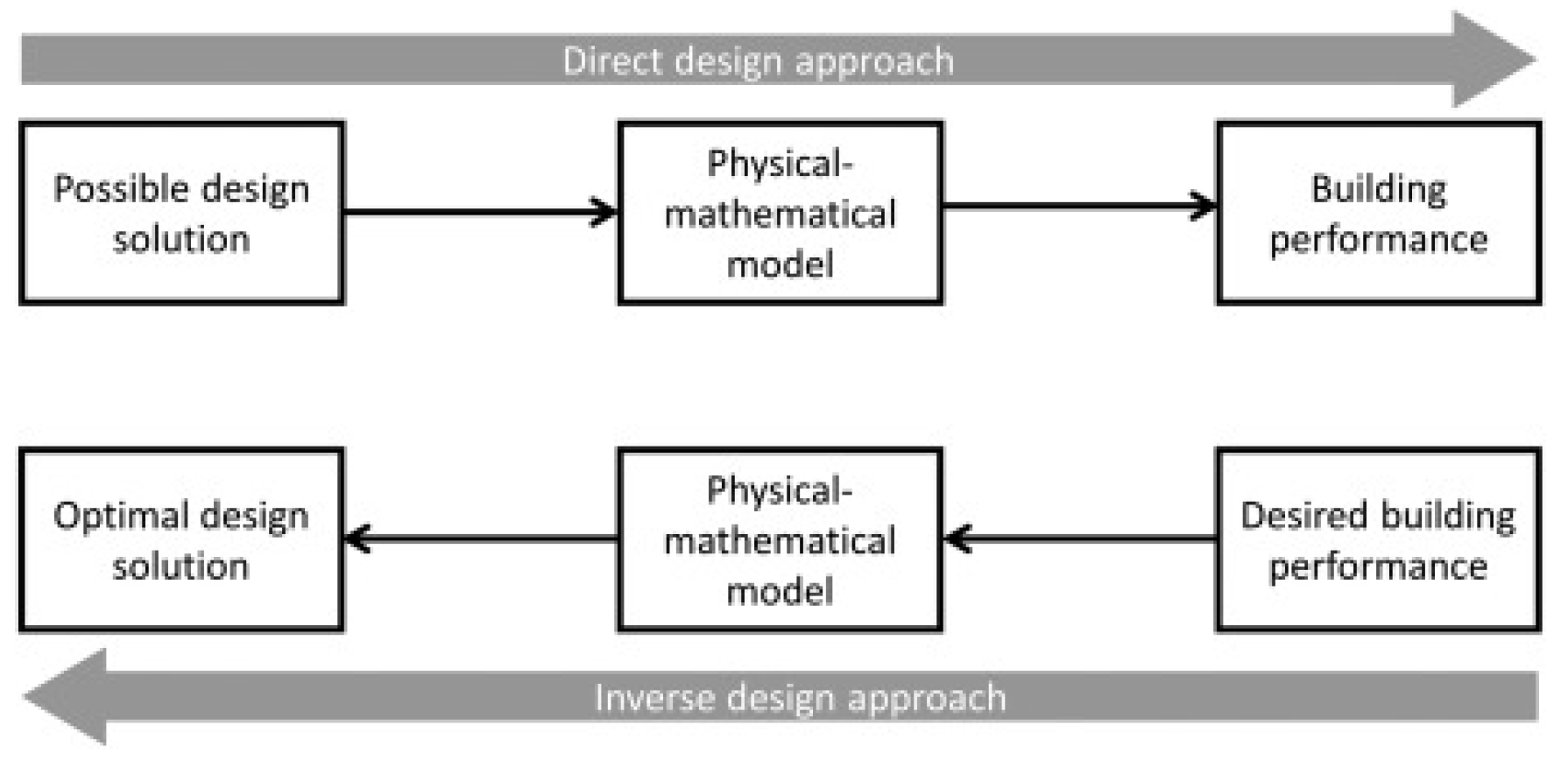
  119. Loonen, R.C.; de Vries, S.; Goia, F. Inverse design for advanced building envelope materials, systems and operation. In Rethinking Building Skins; Elsevier: Amsterdam, The Netherlands, 2022; pp. 377–402. [Google Scholar]
  120. Piggott, A.Y.; Petykiewicz, J.; Su, L.; Vučković, J. Fabrication-constrained nanophotonic inverse design. Sci. Rep. 2017, 7, 1786. [Google Scholar] [CrossRef] [PubMed]
  121. Kim, J.; Kim, J.Y.; Yoon, J.; Yoon, H.; Park, H.H.; Kurt, H. Experimental demonstration of inverse-designed silicon integrated photonic power splitters. Nanophotonics 2022, 11, 4581–4590. [Google Scholar] [CrossRef]
  122. Qiu, C.; Sheng, Z.; Li, H.; Liu, W.; Li, L.; Pang, A.; Wu, A.; Wang, X.; Zou, S.; Gan, F. Fabrication, Characterization and Loss Analysis of Silicon Nanowaveguides. J. Light. Technol. 2014, 32, 2303–2307. [Google Scholar] [CrossRef]
  123. Sheng, Z.; Dai, D.; He, S. Comparative study of losses in ultrasharp silicon-on-insulator nanowire bends. IEEE J. Sel. Top. Quantum Electron. 2009, 15, 1406–1412. [Google Scholar] [CrossRef]
  124. Vlasov, Y.A.; McNab, S.J. Losses in single-mode silicon-on-insulator strip waveguides and bends. Opt. Express 2004, 12, 1622–1631. [Google Scholar] [CrossRef]
  125. Mashanovich, G.Z.; Gardes, F.Y.; Thomson, D.J.; Hu, Y.; Li, K.; Nedeljkovic, M.; Soler Penades, J.; Khokhar, A.Z.; Mitchell, C.J.; Stankovic, S.; et al. Silicon Photonic Waveguides and Devices for Near- and Mid-IR Applications. IEEE J. Sel. Top. Quantum Electron. 2015, 21, 407–418. [Google Scholar] [CrossRef]
  126. Selvaraja, S.K.; Sethi, P. Review on optical waveguides. Emerg. Waveguide Technol. 2018, 95, 458. [Google Scholar]
  127. Hong, S.; Zhang, L.; Wang, Y.; Zhang, M.; Xie, Y.; Dai, D. Ultralow-loss compact silicon photonic waveguide spirals and delay lines. Photonics Res. 2022, 10, 1–7. [Google Scholar] [CrossRef]
  128. Wu, S.; Mu, X.; Cheng, L.; Mao, S.; Fu, H. State-of-the-art and perspectives on silicon waveguide crossings: A review. Micromachines 2020, 11, 326. [Google Scholar] [CrossRef]
  129. Tsarev, A.V. Efficient silicon wire waveguide crossing with negligible loss and crosstalk. Opt. Express 2011, 19, 13732–13737. [Google Scholar] [CrossRef]
  130. Bogaerts, W.; Dumon, P.; Van Thourhout, D.; Baets, R. Low-loss, low-cross-talk crossings for silicon-on-insulator nanophotonic waveguides. Opt. Lett. 2007, 32, 2801–2803. [Google Scholar] [CrossRef]
  131. Sun, H.; Qiao, Q.; Guan, Q.; Zhou, G. Silicon photonic phase shifters and their applications: A review. Micromachines 2022, 13, 1509. [Google Scholar] [CrossRef]
  132. Quack, N.; Takabayashi, A.Y.; Sattari, H.; Edinger, P.; Jo, G.; Bleiker, S.J.; Errando-Herranz, C.; Gylfason, K.B.; Niklaus, F.; Khan, U.; et al. Integrated silicon photonic MEMS. Microsystems Nanoeng. 2023, 9, 27. [Google Scholar] [CrossRef] [PubMed]
  133. Edinger, P.; Takabayashi, A.Y.; Errando-Herranz, C.; Khan, U.; Sattari, H.; Verheyen, P.; Bogaerts, W.; Quack, N.; Gylfason, K.B. Silicon photonic microelectromechanical phase shifters for scalable programmable photonics. Opt. Lett. 2021, 46, 5671–5674. [Google Scholar] [CrossRef] [PubMed]
  134. Sattari, H.; Graziosi, T.; Kiss, M.; Seok, T.J.; Han, S.; Wu, M.C.; Quack, N. Silicon photonic MEMS phase-shifter. Opt. Express 2019, 27, 18959–18969. [Google Scholar] [CrossRef] [PubMed]
  135. Baghdadi, R.; Gould, M.; Gupta, S.; Tymchenko, M.; Bunandar, D.; Ramey, C.; Harris, N.C. Dual slot-mode NOEM phase shifter. Opt. Express 2021, 29, 19113–19119. [Google Scholar] [CrossRef] [PubMed]
  136. Xin, C.; Zhang, Z.; Wang, X.; Fan, C.; Li, M. Ultracompact single-layer optical MEMS accelerometer based on evanescent coupling through silicon nanowaveguides. Sci. Rep. 2022, 12, 21697. [Google Scholar] [CrossRef] [PubMed]
  137. Chiu, W.C.; Chang, C.C.; Wu, J.M.; Lee, M.C.M.; Shieh, J.M. Optical phase modulators using deformable waveguides actuated by micro-electro-mechanical systems. Opt. Lett. 2011, 36, 1089–1091. [Google Scholar] [CrossRef]
  138. Song, L.; Li, H.; Dai, D. Mach–Zehnder silicon-photonic switch with low random phase errors. Opt. Lett. 2021, 46, 78–81. [Google Scholar] [CrossRef]
  139. Sabouri, S.; Mendoza Velasco, L.A.; Catuneanu, M.; Namdari, M.; Jamshidi, K. Thermo Optical Phase Shifter With Low Thermal Crosstalk for SOI Strip Waveguide. IEEE Photonics J. 2021, 13, 1–12. [Google Scholar] [CrossRef]
  140. Singh, T.; Khaira, N.K.; Mansour, R.R. Thermally Actuated SOI RF MEMS-Based Fully Integrated Passive Reflective-Type Analog Phase Shifter for mmWave Applications. IEEE Trans. Microw. Theory Tech. 2021, 69, 119–131. [Google Scholar] [CrossRef]
  141. Gao, W.; Li, X.; Lu, L.; Liu, C.; Chen, J.; Zhou, L. Broadband 32× 32 Strictly-Nonblocking Optical Switch on a Multi-Layer Si3N4-on-SOI Platform. Laser Photonics Rev. 2023, 17, 2300275. [Google Scholar] [CrossRef]
  142. Wang, J.; Cheng, W.; Zhu, W.; Lu, M.; Chen, Y.; Shi, S.; Guo, C.; Hu, G.; Cui, Y.; Yun, B. Optimization and comprehensive comparison of thermo-optic phase shifter with folded waveguide on SiN and SOI platforms. Opt. Commun. 2024, 555, 130242. [Google Scholar] [CrossRef]
  143. Gao, F.; Xie, W.; Tan, J.Y.S.; Leong, C.; Li, C.; Luo, X.; Lo, G.Q. Comprehensive Investigation of Thermo-Optic Phase Shifters on a Multi-Layered SiN-on-SOI Platform. J. Light. Technol. 2023, 41, 3108–3114. [Google Scholar] [CrossRef]
  144. Zhong, C.; Zhang, Z.; Ma, H.; Wei, M.; Ye, Y.; Wu, J.; Tang, B.; Zhang, P.; Liu, R.; Li, J.; et al. Silicon thermo-optic switches with graphene heaters operating at mid-infrared waveband. Nanomaterials 2022, 12, 1083. [Google Scholar] [CrossRef]
  145. Yan, S.; Zhu, X.; Frandsen, L.H.; Xiao, S.; Mortensen, N.A.; Dong, J.; Ding, Y. Slow-light-enhanced energy efficiency for graphene microheaters on silicon photonic crystal waveguides. Nat. Commun. 2017, 8, 14411. [Google Scholar] [CrossRef] [PubMed]
  146. Parra, J.; Hurtado, J.; Griol, A.; Sanchis, P. Ultra-low loss hybrid ITO/Si thermo-optic phase shifter with optimized power consumption. Opt. Express 2020, 28, 9393–9404. [Google Scholar] [CrossRef]
  147. Jacques, M.; Samani, A.; El-Fiky, E.; Patel, D.; Xing, Z.; Plant, D.V. Optimization of thermo-optic phase-shifter design and mitigation of thermal crosstalk on the SOI platform. Opt. Express 2019, 27, 10456–10471. [Google Scholar] [CrossRef]
  148. Harris, N.C.; Ma, Y.; Mower, J.; Baehr-Jones, T.; Englund, D.; Hochberg, M.; Galland, C. Efficient, compact and low loss thermo-optic phase shifter in silicon. Opt. Express 2014, 22, 10487–10493. [Google Scholar] [CrossRef]
  149. Qiu, H.; Liu, Y.; Luan, C.; Kong, D.; Guan, X.; Ding, Y.; Hu, H. Energy-efficient thermo-optic silicon phase shifter with well-balanced overall performance. Opt. Lett. 2020, 45, 4806–4809. [Google Scholar] [CrossRef]
  150. Miller, S.A.; Chang, Y.C.; Phare, C.T.; Shin, M.C.; Zadka, M.; Roberts, S.P.; Stern, B.; Ji, X.; Mohanty, A.; Gordillo, O.A.J.; et al. Large-scale optical phased array using a low-power multi-pass silicon photonic platform. Optica 2020, 7, 3–6. [Google Scholar] [CrossRef]
  151. Fang, Z.; Chen, R.; Zheng, J.; Khan, A.I.; Neilson, K.M.; Geiger, S.J.; Callahan, D.M.; Moebius, M.G.; Saxena, A.; Chen, M.E.; et al. Ultra-low-energy programmable non-volatile silicon photonics based on phase-change materials with graphene heaters. Nat. Nanotechnol. 2022, 17, 842–848. [Google Scholar] [CrossRef] [PubMed]
  152. Sobu, Y.; Simoyama, T.; Tanaka, S.; Tanaka, Y.; Morito, K. 70 Gbaud Operation of All-Silicon Mach–Zehnder Modulator based on Forward-Biased PIN Diodes and Passive Equalizer. In Proceedings of the 2019 24th OptoElectronics and Communications Conference (OECC) and 2019 International Conference on Photonics in Switching and Computing (PSC), Fukuoka, Japan, 7–11 July 2019; pp. 1–3. [Google Scholar] [CrossRef]
  153. Li, X.; Xiao, X.; Xu, H.; Li, Z.; Chu, T.; Yu, J.; Yu, Y. Highly Efficient Silicon Michelson Interferometer Modulators. IEEE Photonics Technol. Lett. 2013, 25, 407–409. [Google Scholar] [CrossRef]
  154. Ziebell, M.; Marris-Morini, D.; Rasigade, G.; Fédéli, J.M.; Crozat, P.; Cassan, E.; Bouville, D.; Vivien, L. 40 Gbit/s low-loss silicon optical modulator based on a pipin diode. Opt. Express 2012, 20, 10591–10596. [Google Scholar] [CrossRef] [PubMed]
  155. Tu, X.; Liow, T.Y.; Song, J.; Luo, X.; Fang, Q.; Yu, M.; Lo, G.Q. 50-Gb/s silicon optical modulator with traveling-wave electrodes. Opt. Express 2013, 21, 12776–12782. [Google Scholar] [CrossRef]
  156. Azadeh, S.S.; Merget, F.; Romero-García, S.; Moscoso-Mártir, A.; von den Driesch, N.; Müller, J.; Mantl, S.; Buca, D.; Witzens, J. Low V π Silicon photonics modulators with highly linear epitaxially grown phase shifters. Opt. Express 2015, 23, 23526–23550. [Google Scholar] [CrossRef]
  157. Li, M.; Wang, L.; Li, X.; Xiao, X.; Yu, S. Silicon intensity Mach–Zehnder modulator for single lane 100 Gb/s applications. Photonics Res. 2018, 6, 109–116. [Google Scholar] [CrossRef]
  158. Begović, A.; Kim, Y.H.; Jiang, L.; Anderson, S.; Huang, Z.R. Low VπLπ and Driving Voltage Interleaved Silicon Phase Shifter for Modulation Applications. IEEE Photonics J. 2022, 14, 1–6. [Google Scholar] [CrossRef]
  159. Cai, H.; Fu, S.; Yu, Y.; Zhang, X. Lateral-Zigzag PN Junction Enabled High-Efficiency Silicon Micro-Ring Modulator Working at 100Gb/s. IEEE Photonics Technol. Lett. 2022, 34, 525–528. [Google Scholar] [CrossRef]
  160. Nivethitha, V.; Sivasubramanian, A. Design and simulate the demultiplexer using photonic crystal ring resonator for DWDM system. Opt. Quantum Electron. 2024, 56, 98. [Google Scholar] [CrossRef]
  161. Westerveld, W.J.; Mahmud-Ul-Hasan, M.; Shnaiderman, R.; Ntziachristos, V.; Rottenberg, X.; Severi, S.; Rochus, V. Sensitive, small, broadband and scalable optomechanical ultrasound sensor in silicon photonics. Nat. Photonics 2021, 15, 341–345. [Google Scholar] [CrossRef]
  162. Kazanskiy, N.L.; Khonina, S.N.; Butt, M.A. A Review of Photonic Sensors Based on Ring Resonator Structures: Three Widely Used Platforms and Implications of Sensing Applications. Micromachines 2023, 14, 1080. [Google Scholar] [CrossRef]
  163. Paschotta, R. Q Factor. RP Photonics Encyclopedia. 2006. Available online: https://www.rp-photonics.com/q_factor.html (accessed on 13 May 2024).
  164. Kumari, S.; Prince, S. Photonic Beamforming Incorporating Ring Resonator Based on Silicon-on-Insulator Waveguide Technology. Silicon 2022, 14, 8869–8879. [Google Scholar] [CrossRef]
  165. Robinson, J.T.; Chen, L.; Lipson, M. On-chip gas detection in silicon optical microcavities. Opt. Express 2008, 16, 4296–4301. [Google Scholar] [CrossRef] [PubMed]
  166. Rodriguez, G.A.; Hu, S.; Weiss, S.M. Porous silicon ring resonator for compact, high sensitivity biosensing applications. Opt. Express 2015, 23, 7111–7119. [Google Scholar] [CrossRef]
  167. Kundal, S.; Khandelwal, A. Improving the performance of ring resonator refractive index sensor through structural modifications. Optik 2024, 296, 171555. [Google Scholar] [CrossRef]
  168. Saha, N.; Brunetti, G.; di Toma, A.; Armenise, M.N.; Ciminelli, C. Silicon Photonic Filters: A Pathway from Basics to Applications. Adv. Photonics Res. 2024, 2300343. [Google Scholar] [CrossRef]
Figure 1. Schematic of optical interconnections between fiber and photonic chip [10].
Photonics 11 00494 g001
Figure 2. Schematic of Si photonic couplers based on (a) a multi-tip taper and (b) multiple tapers [10].
Photonics 11 00494 g002
Figure 3. Three-dimensionalschematic of a multiple-taper edge coupler [34].
Photonics 11 00494 g003
Figure 4. Silicon inverse taper assisted with multiple waveguides (cross-section view) [10].
Photonics 11 00494 g004
Figure 5. Multi-stage tapers with a forward taper [10].
Photonics 11 00494 g005
Figure 6. Schematic structure of a 1D-GC with a linear waveguide taper and key parameters: period Λ , fiber tilt angle θ , varying taper width W, and taper angle θ t a p e r . In blue Silicon, in red the light signal [11].
Photonics 11 00494 g006
Figure 7. Schematic of planar waveguide grating and its parameters [11].
Photonics 11 00494 g007
Figure 8. Schematic of quasiplanar coupling. Reproduced from [68]. The red arrow represents the light beam.
Photonics 11 00494 g008
Figure 9. (a) GC with poly-silicon overlay [69]; (b) GC with metal reflector [72]. Picture from [11].
Photonics 11 00494 g009
Figure 10. (a) GC with double etch steps; (b) slanted GC (upper) and dual-layer GC (lower). Picture from [11].
Photonics 11 00494 g010
Figure 11. Two-dimensional PSGC with TE/TM polarizations coupled to TE0 waveguide modes in orthogonal directions; picture from [11].
Photonics 11 00494 g011
Figure 12. Comparison of four main beam splitting methods [84].
Photonics 11 00494 g012
Figure 13. Schematic design of a directional coupler with its parameters [95].
Photonics 11 00494 g013
Figure 14. Schematic geometry of two standard 3 dB-MMIs [111].
Photonics 11 00494 g014
Figure 15. Schematic representation of inverse design in comparison to direct design approach [120].
Photonics 11 00494 g015
Figure 16. Semi-quantitative comparison between available methods for silicon photonic phase shifters [131].
Photonics 11 00494 g016
Figure 17. MEMS phase shifters based on evanescent field perturbation by (a) a silicon beam above the bus waveguide, (b) with a cutoff width silicon beam next to the bus waveguide; confined optical mode modulation through (c) a slot waveguide and a (d) dual slot waveguide; and modulating the optical path length through (e) a deformable waveguide and a (f) horizontal directional coupler. Image reproduced from [131].
Photonics 11 00494 g017
Figure 18. Various structures of thermo-optic (t-o) shifters. (a) Traditional t-o phase shifter, (b) t-o phase shifter with air trench, (c) t-o phase shifter with 2D material heaters, (d) t-o phase shifter with doping silicon heater, (e1) bended t-o phase shifter with doping silicon heater, and (e2) its cross-sectional schematic. Image reproduced by [131].
Photonics 11 00494 g018
Figure 20. Resonance wavelength shift in the RR due to the change in the ambient RI. Image reproduced from [162].
Photonics 11 00494 g020
Disclaimer/Publisher’s Note: The statements, opinions and data contained in all publications are solely those of the individual author(s) and contributor(s) and not of MDPI and/or the editor(s). MDPI and/or the editor(s) disclaim responsibility for any injury to people or property resulting from any ideas, methods, instructions or products referred to in the content.

