Article

Efficient Structure Transformation Based on Sensitivity-Oriented Structure Adjustment for Inverse-Designed Devices

School of Electronic Engineering, Beijing University of Posts and Telecommunications, Beijing 100876, China
*
Author to whom correspondence should be addressed.
Photonics 2024, 11(3), 265; https://doi.org/10.3390/photonics11030265
Submission received: 24 January 2024 / Revised: 5 March 2024 / Accepted: 8 March 2024 / Published: 14 March 2024
(This article belongs to the Special Issue Design and Applications of Novel Nanophotonics Devices)

Abstract

:
Inverse-designed devices with thousands of degrees of freedom could achieve high performance in compact footprints, but typically have complex structure topologies that contain many irregular and tiny features and sharp corners, which tend to lead to a poor robustness to fabrication errors. In order to effectively transform the structure of inverse-designed nanophotonic devices into simple structure topologies that have high robustness to fabrication errors without sacrificing device performance, in this paper, we propose a structure adjustment method that innovatively adjusts the structures of inverse-designed devices by introducing their structural sensitivity to the optical performance, extracting the device substructures with high sensitivity and eliminating those with low sensitivity, and, finally, transforming the device structures into simple structure topologies with high robustness and better performance. Two devices (90° crossing and T-junction) were designed and fabrication tolerance simulation was conducted to verify the method. The results show that the devices designed using the proposed method achieved better performance and were more robust to under/over-etched errors.

1. Introduction

The inverse design method has been a powerful tool in nanophotonics due to its powerful capability of designing devices with compact footprints, high performance, and flexible functions [1,2,3]. Its excellent design capability is attributed to the computational mechanisms that explore the full design space of devices with thousands or millions of degrees of freedom through gradient-based algorithm optimization. However, the mechanisms also make inverse-designed devices typically have complex structure topologies that contain numbers of irregular and tiny features, as well as sharp corners, which tend to lead to a poor robustness to fabrication errors and potential performance degradation. Reducing tiny features and smoothing the sharp corners are common ideas to reduce the uncertainties in fabrication. Many efforts have been made to take such fabrication constraints and uncertainties into account in the process of inverse design through imposing constraints such as curvature and feature size in differentiable forms and introducing them into the iterative optimization process [4,5,6,7,8]. This scheme is well suited for free-form devices due to its compatibility with efficient gradient-based optimization algorithms. However, as they are based on local optimizers and converge to local solutions in non-convex optimizations, they are sensitive to the initial structures, which are difficult to predetermine without theoretical analysis and expertise. Additionally, there is a general tendency for the optical performance of the final designed devices to degrade with more demanding constraints [8,9]. There are schemes supported by machine learning techniques [10,11,12] that integrate geometric constraints into the design process and offer global search and analysis capabilities, preventing the convergence to inferior local minima. However, these schemes are practically limited in devices with few degrees of freedom or 2D/2.5D simulated devices. This limitation is due to the exponential increase in the required number of samples or simulations with the increase in the number of design parameters, which makes the computational cost for 3D device design impractically high.
On the other hand, there is another kind of inverse design method that optimizes a relative regular structure starting from an empirical pattern based on physical principles [13,14,15,16], i.e., a physics-guided structure with the adjoint method. With such physical-principle-based initial structures, the optimized structures of these typical devices are similar to conventional devices. The constraints of the curvature and feature sizes can also be introduced into such a method [13], helping these devices to potentially achieve high performance as well as high robustness in fabrication, making them well suited for rapid industrial adoption. Besides, our previous work demonstrated that typical simple structures can be achieved not only through physics-guided methods, but also via the structure transformation (ST) technique that we introduced [17]. The ST technique is based on a strategy that alternately implements optical performance optimization (OPO) and modified level-set-based curvature-constrained structure adjustment (SA). This technique has been proven to transform device structures into simpler structure topologies that have better performance and are much more robust to fabrication errors without the requirement for an elaborately predetermined initial structure. The core of ST lies in enforcing perturbations on OPO-optimized structures through SA, updating the initial structure for the subsequent OPO. However, for the ST technique in [17], the structure is adjusted primarily according to the geometric characteristics, overlooking the structural sensitivity to optical performance. For this reason, the ST inherently necessitates multiple rounds of SA-OPO optimization, which cannot be implemented in parallel.
In this work, we propose a new SA method, termed sensitivity-oriented structure adjustment (SOSA), which effectively simplifies device structures according to the structural sensitivity to their optical performance. SOSA employs a modified Active Contour Model in Distance Regularized Level Set Evolution (ACM-DRLSE) [18] with a weighted edge indicator function, which incorporates the structural sensitivity of the previously OPO-optimized structure, to extract the substructures with high sensitivity and eliminate those with low sensitivity. By introducing SOSA as a preliminary step in the original ST [17], a modified structure transformation technique is proposed, termed ST with SOSA (ST-SOSA). Applying ST-SOSA, the simpler device structure with enhanced optical performance and fabrication robustness is realized in a few optimization rounds. Demonstratively, two devices (90° crossing and T-junction) are designed using the general inverse design method [19,20] and then transformed by ST-SOSA. The new 90° crossing and T-junction were realized within three and four rounds of optimization. Through ST-SOSA, the simulated maximum insertion loss (IL), in the wavelength of 1480–1580 nm, of the T-junction (90° crossing) reduced from 1.6 dB (0.59 dB) to 0.3 1 dB (0.34 dB). The maximum crosstalk (CT) of the 90° crossing reduced from −25.42 dB to −31.65 dB. Finally, the fabrication tolerance simulation was implemented to verify that the devices with ST-SOSA were more robust to over/under-etching errors than those without ST-SOSA.

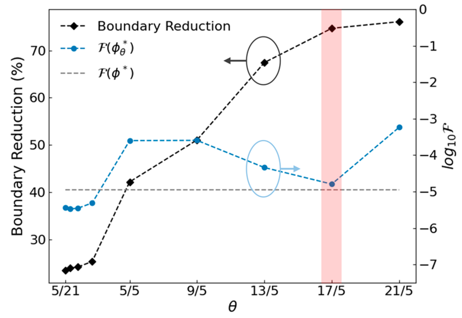
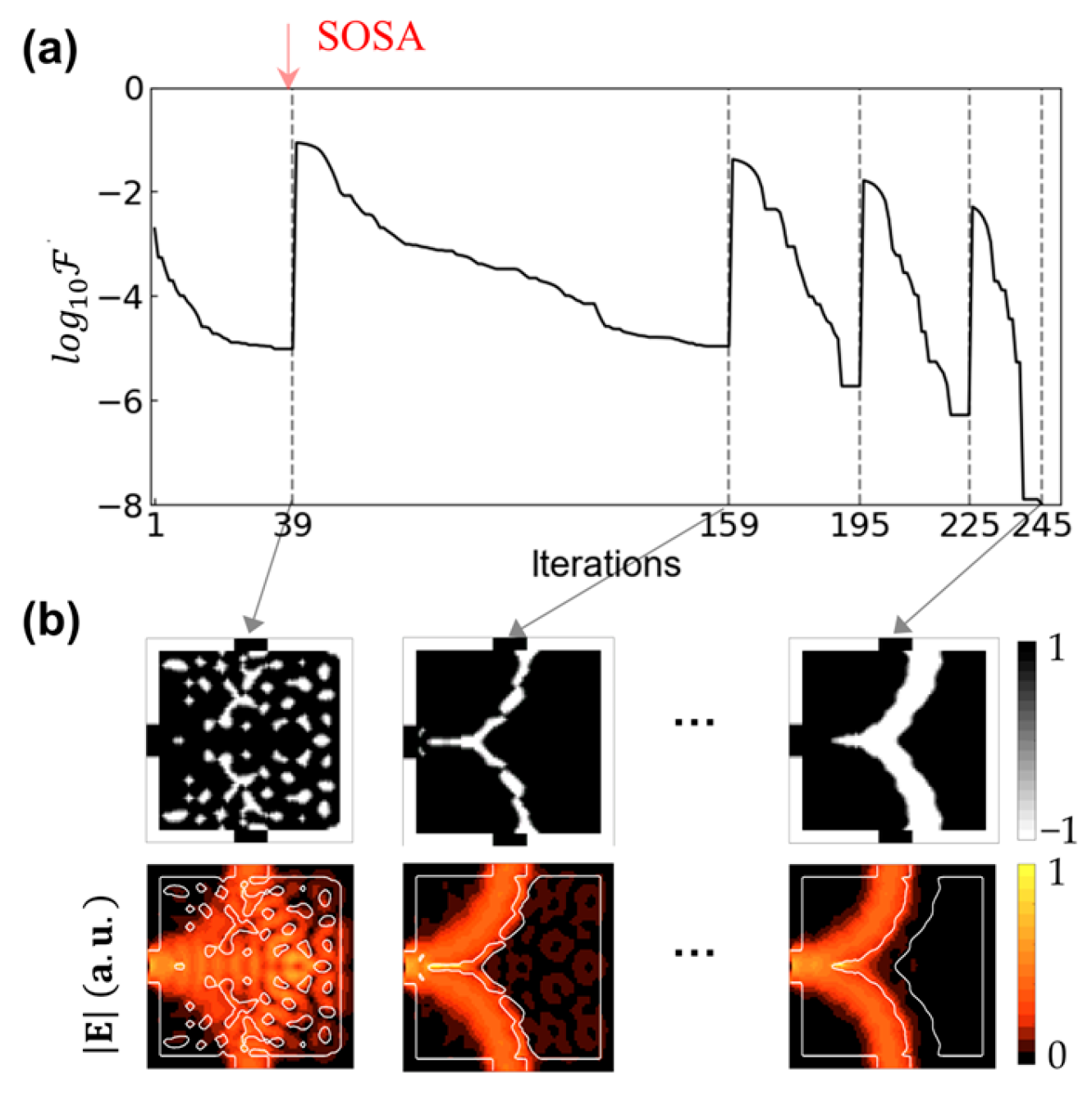
2. Sensitivity-Oriented Structure Adjustment (SOSA)

The ST technique is based on a strategy that alternately implements optical performance optimization (OPO) and structure adjustment (SA). OPOs are used to optimize the device structures with respect to the desired optical performance, while SAs are used to reinitialize the structure for a subsequent OPO by adjusting the previously OPO-optimized structure [17]. In this work, we propose a new method termed SOSA, as a preliminary step in ST, to efficiently adjust the structure and improve the efficiency of the device structure simplification. Figure 1 shows the process of the proposed ST with SOSA (ST-SOSA) applied in designing a 90° crossing, in which the TE0 mode is injected into Port 0 (1) and expected to output from Port 2 (3).
The process of ST-SOSA is divided into two parts. In the first part, the device structure is efficiently simplified through SOSA and a subsequent OPO (a single SOSA-OPO round). In the second part, the process of the original ST [17] is applied to further smooth and optimize the simplified structures. The proposed SOSA leverages a modified ACM-DRLSE with a weighted edge indicator function, which incorporates the structural sensitivity of the previously optimized structure, to effectively extract and retain the substructures with high sensitivity to optical performance in the optimized devices and eliminate those with low sensitivity. The basic principles of OPO and ACM-DRLSE are briefly overviewed in Section 2.1 and Section 2.2, respectively. The principle of the proposed SOSA method based on a modified ACM-DRLSE is introduced in Section 2.3.

2.1. Optical Performance Optimization (OPO)
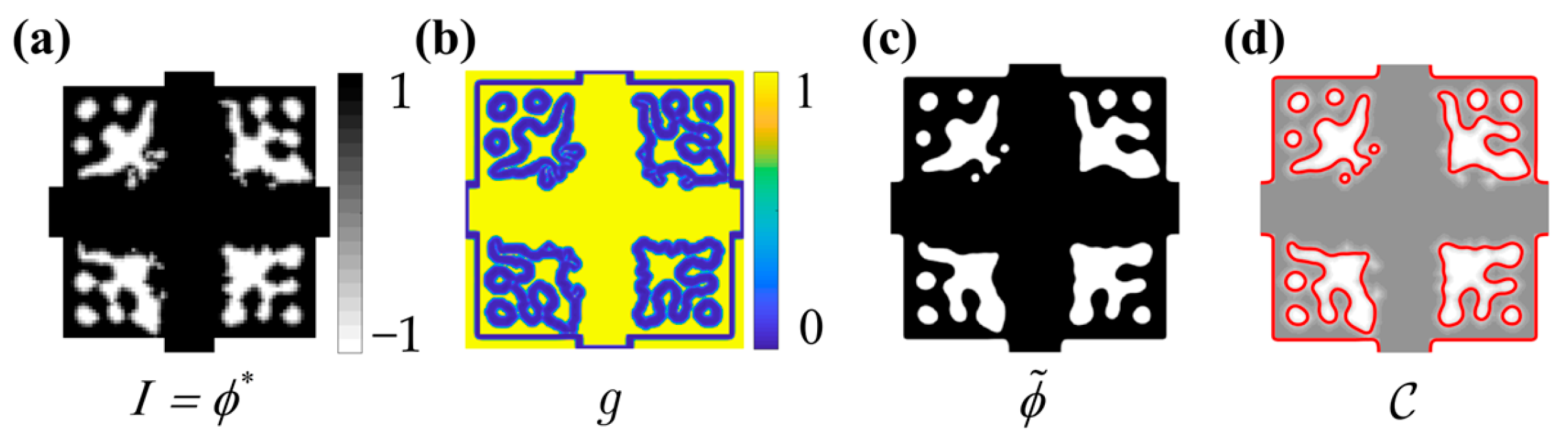
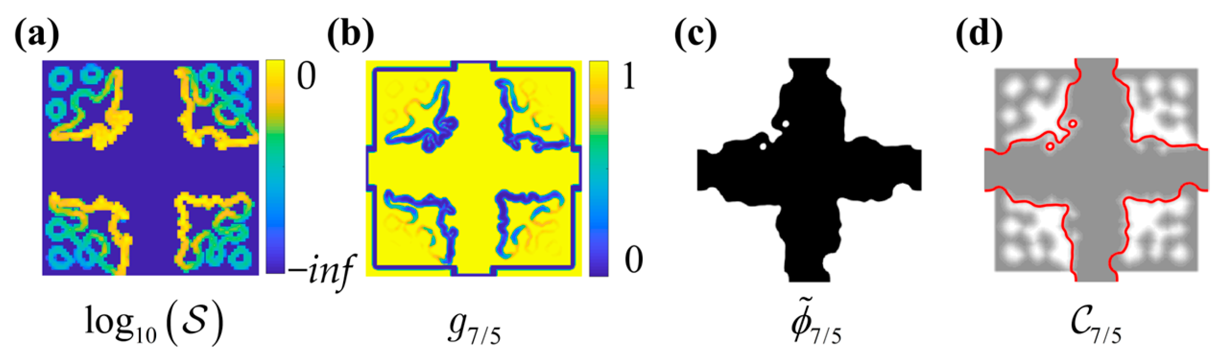
The objective function in OPO for the devices is defined as:
E 1 ϕ , E 2 ϕ , , E i ϕ = j = 1 M i = 1 N I + 2 α i j i j E i ϕ + I + 2 i j E i ϕ β i j
where i j is a linear function that represents the overlap ratio between the monitored electric field E i and the desired mode field over the cross section of the j th of M output ports for the ith mode, and the optimized variable ϕ is the level set representation of the binary device structure. i j 2 E i ϕ is bounded between the minimum value α i j [ 0 , 1 ] and maximum value β i j [ α i j , 1 ] according to the desired output power. The steepest descent optimization is performed to meet the desired optical performance [19,20], where the local optimal solution is denoted as ϕ * : = arg min F ϕ . The three-dimensional finite-difference frequency-domain (3D FDFD) method is used to calculate the optical response from the structures of devices and the Maxwell solver package developed by Jesse Lu et al., at Stanford University is available in [21].

2.2. ACM-DRLSE

The active contour model (ACM) is a popular technique used in computer vision and image processing for image segmentation and object boundary detection [22,23]. The essence of ACM is to evolve a curve (or contour) 𝒞 to signify the target boundary of an image I , which is usually accomplished by minimizing an energy function by means of the standard descent method. To flexibly represent contours of complex topology and handle topological changes, the curve evolution in terms of 𝒞 is always converted to a level set formulation by representing 𝒞 as the zero-level set of a higher dimensional function ϕ , named level set function (LSF) [24]. Then, the motion of the zero-level set (or contour) is formulated as the evolution of the LSF. Further, to address the challenges faced by traditional level set methods—numerical errors due to deviation from a signed distance function and increased computational complexity from necessary but costly re-initialization steps—ACM-DRLSE was proposed [18]. ACM-DRLSE introduced a distance regularization term into the level set evolution equation to ensure that the level set function maintains a signed distance profile throughout its evolution. The energy function of ACM-DRLSE is given as:
E ε ϕ = μ R p ϕ + λ Ω g δ ε ϕ ϕ d x + α Ω g H ε ϕ d x
In Equation (2), R p is the distance regularization term defined with a double-well potential function p that penalizes the LSF when it deviates from a signed distance function. The other two terms in the right of Equation (2) are associated with an edge indicator function g , which is commonly defined as:
g 1 1 + G σ I 2
where G σ I denotes convolving image I with a Gaussian kernel whose standard deviation is σ . Thus, Ω g δ ε ϕ ϕ d x is the level set formulation of the energy function of the classic Geodesic Active Contour (GAC) model [24], which stops the contour evolution on object boundaries, and Ω g H ε ϕ d x is introduced to speed up the motion of the zero-level contour in the level set evolution process, especially when the contour is far away from the desired object boundaries, encouraging the contour to expand or shrink.
A curve 𝒞 is evolved to signify the target boundary by minimizing Equation (2). The corresponding level set evolution equation is obtained through the computation of the Euler–Lagrange of Equation (2) [24,25] as:
ϕ t = E ϕ = μ R p ϕ + λ δ ε ϕ d i v g ϕ ϕ + α g δ ε ϕ
where δ ε is the approximate forms of Dirac function as Equation (5), and μ , λ , and α are the weight parameters of the three terms. The details of R p and R p ϕ are described in Section 1 in the Supplementary Materials.
δ ε x = 1 2 ε 1 + cos π x ε , x ε 0 , x > ε
Taking 90° crossing as an example, the process of signifying the boundary of the device structure is described as follows. The inverse-designed (OPO-optimized) structure ϕ * is treated as a quasi-binary image, as shown in Figure 2a, with unknown boundaries 𝒞*. When evolving an LSF ϕ through Equation (4) with an initialized LSF ϕ t = 0 = ϕ 0 , where ϕ 0 is an initial prediction of ϕ * , the zero-level contour 𝒞 of ϕ will stop when it meets the zero-level contour of ϕ * , as shown in Figure 2d, where ϕ is denoted as ϕ ˜ , as shown in Figure 2c.

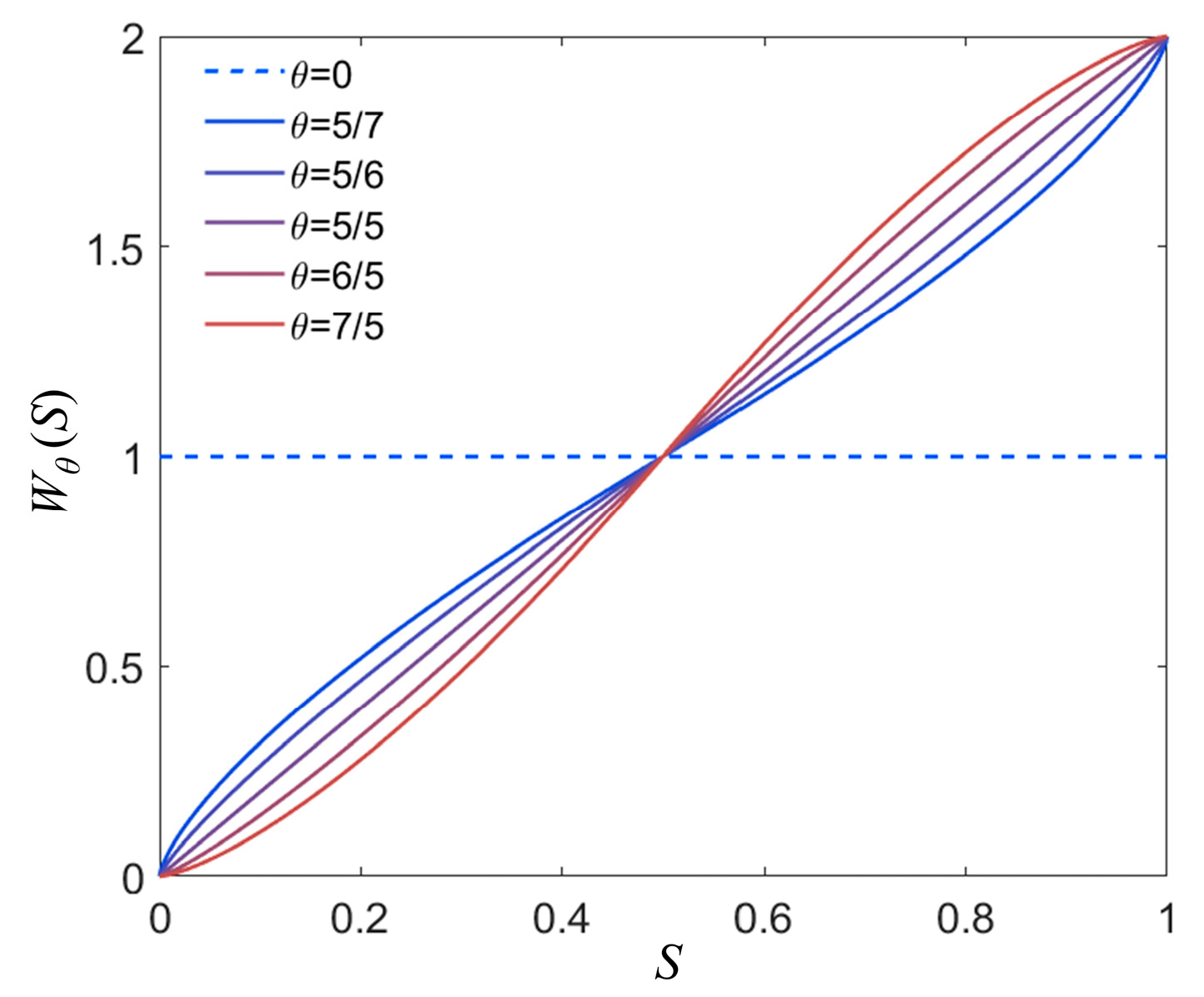
2.3. SOSA Based on the Modified ACM-DRLSE

As described in Section 2.2, Equation (4), with the common edge indicator function, will evolve ϕ to nearly completely recreate the OPO-optimized structure ϕ * . This process does not serve to adjust the structure and update the initial structure for the subsequent OPO. For the purpose of simplifying the structure ϕ * by only extracting the effective substructures of ϕ * , the curves 𝒞 are expected to stop when encountering partial boundaries with high structural sensitivity, whereas they pass through when encountering other boundaries. Therefore, we propose a weighted edge indicator:
g θ 1 1 + G σ ϕ * 2 W θ S
W θ S = 2 S θ S 0.5 2 2 2 S θ S > 0.5
where the structural sensitivity S is defined by the magnitude of the gradient of the versus ϕ as S = ϕ E ϕ , and W θ S is a set of non-linear mappings corresponding to different θ , defined as Equation (7). Figure 3 illustrates the mappings under different θ . Specifically, Equation (6) degenerates into Equation (3) when θ = 0 .
With the proposed weighted edge indicator function, the level set evolution of the LSF ϕ θ with a specific θ is modified as:
ϕ θ t = μ R p ϕ + λ δ ε ϕ θ div g θ ϕ θ ϕ θ + α g θ δ ε ϕ θ
The first two parameters are fixed as μ = 0.2 , λ = 5 for the devices in this paper, and the parameter α needs to be selected for different devices to determine whether to eliminate isolated Si substructures ( α < 0 ) or SiO2 substructures ( α > 0 ). The mapped structural sensitivity weights different partitions of the edge indicator function, increasing the values of the edge indicator function where the structural sensitivity is low, making the values closer to those in non-edge regions, thereby diminishing its capability to intercept the motion of the curves and allowing the curves to more easily pass through these boundary regions. Conversely, the values of the edge indicator function are decreased in partitions where the structural sensitivity is high, strengthening the constraint on the curves and making the curves stop more readily in these regions. Different θ apply different degrees of weighting to the edge indicator function, resulting in varying degrees of influence on the edge indicator from the sensitivity. Treating ϕ θ as the new device structure, SOSA is realized along with the evolution of ϕ θ . The higher the θ , the more significant the influence of sensitivity on the edge indicator function, and, thus, the more pronounced the adjustments to the structure. Through Equation (8) with different θ , a new set of initial structures for the subsequent round of OPO is obtained. Given that OPOs starting with different initial structures, which are provided by SOSA with different θ , are independent of each other, SOSA with different θ and their subsequent OPOs can be implemented in parallel.
The inverse-designed 90° crossing is shown in Figure 2a, and its structural sensitivity S (in a logarithmic scale) is shown in Figure 4a. Taking the specific case of θ = 7 / 5 as an example, the weighted edge indicator function is illustrated in Figure 4b. Figure 4c,d show the LSF and the corresponding zero level contour obtained through the proposed modified ACM-DRLSE model, respectively. Comparing Figure 2c and Figure 4c, it can be observed that by employing the proposed SOSA method, the substructures of the 90° crossing with high sensitivity are retained, while those with low sensitivity are effectively eliminated. The analyses for cases corresponding to different θ and further optimization are detailed in Section 3.

3. Numerical Example

To demonstrate the applicability and effectiveness of SOSA in device design, the two devices—a crossing and T-junction—were designed with a footprint of 2.8 μm × 2.8 μm and a feature size of 40 nm. The thickness of the etched Si slab, which is completely surrounded by SiO2, is set as 220 nm, where the permittivity values of Si and SiO2 used are ε S i = 12.25 and ε S i O 2 = 2.25 , respectively. In order to reduce the cost of computation, the ST is conducted at a single wavelength 1550 nm. Note that when designing devices for which the properties of wavelength are important, the broadband optimization could be integrated into the ST procedure, which only increases the cost of computation and the ST technique would also work without being modified. In this section, devices operating in the TE0 mode are designed as examples. Nevertheless, the proposed method is equally applicable to design devices operating in other modes, such as the TM mode.

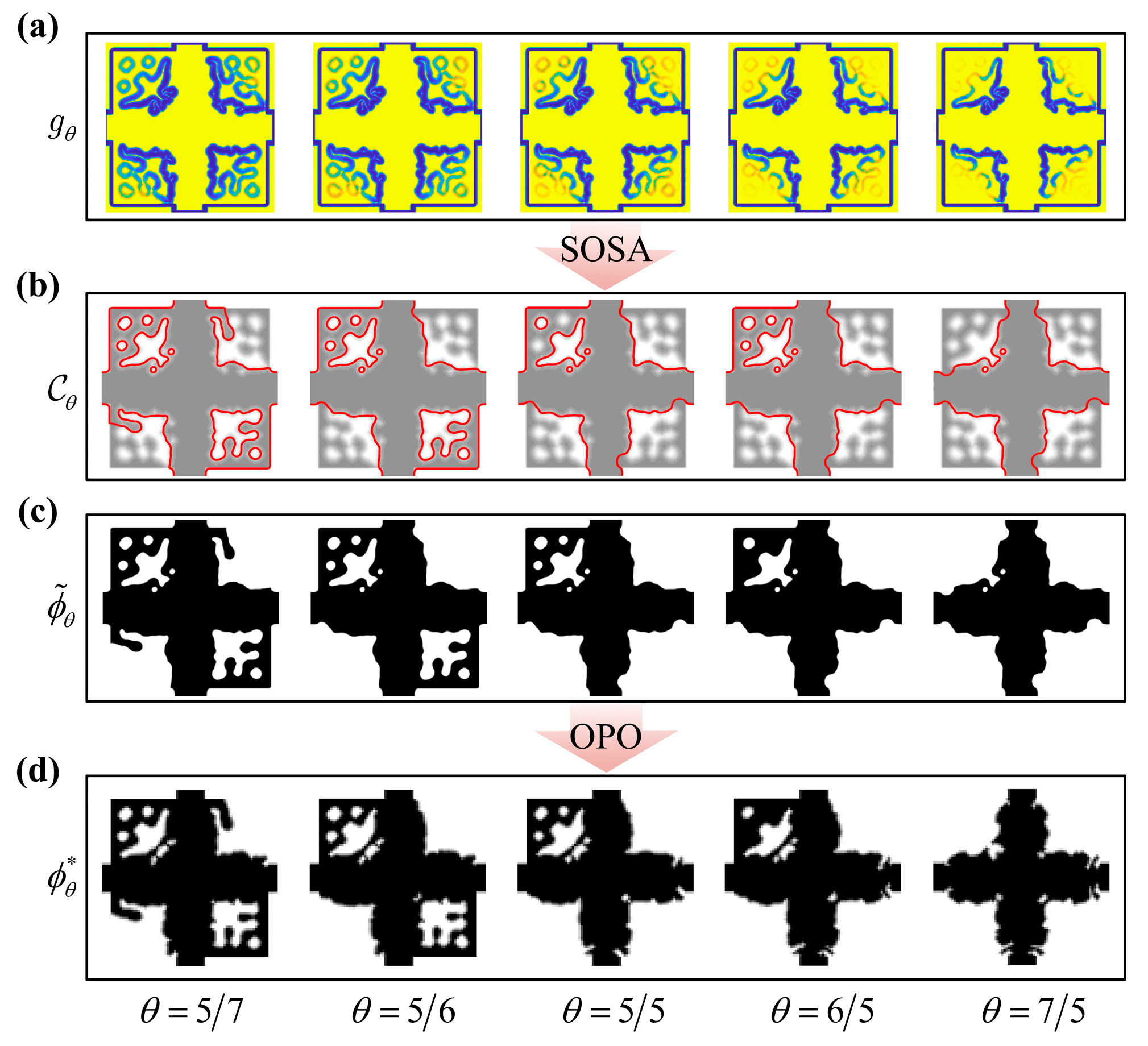
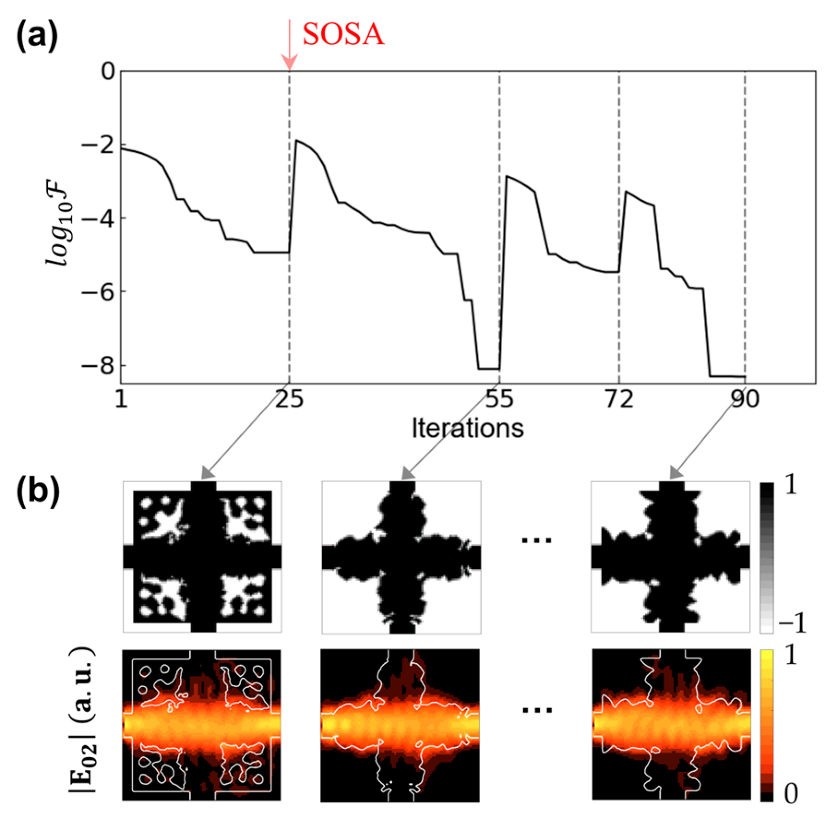
3.1. Design of the 90° Crossing

For the 90° crossing introduced in Section 2, the objective function in OPO was defined as in Equation (1) where the parameters were set as α 12 = α 23 = 0.98 , α 13 = α 22 = 0 , β 12 = β 23 = 1 and β 13 = β 22 = 0.02 . The symmetric design was conducted along the diagonal of the x-axis and y-axis. The process of the SOSA and a subsequent OPO (the SOSA-OPO round) is illustrated in Figure 5, where Figure 5a illustrates the weighted edge indicator defined as Equation (6) with different θ, and the adjusted structures and their corresponding boundaries 𝒞θ after SOSA are shown as Figure 5c,b, respectively. As θ increases, the value of the edge indicator function at the boundaries with low structural sensitivity gradually increases until it approaches 1 (merging with the non-boundary area), thereby diminishing its capability to intercept the motion of the curves. Consequently, the retained boundaries decrease, resulting in simpler structures. Then, OPOs were implemented with the adjusted structures ϕ ˜ θ as initial structures, respectively. The OPO-optimized structures ϕ θ * with initial structures ϕ ˜ θ are shown in Figure 5d.
The percentage reduction in the boundary is utilized as a quantitative measure of the degree of structural simplification. The percentage reduction in the boundary of ϕ θ * compared with that of ϕ * is indicated by a black line in Figure 6. It can be observed that as θ increases, the percentage of the boundary reduction in ϕ θ * gradually increases, and the adjustments to the structure are more pronounced. The objective function values, obtained after SOSA with different θ and the subsequent OPO, are indicated by a blue line, and the previous local optimal value ϕ * before SOSA-OPO is indicated by a gray line for comparison. It can be observed that ϕ θ * < ϕ * holds true for all of the θ , indicating that after the perturbation of local optimum ϕ * by SOSA, the subsequent OPO yields superior local solutions. This implies that the simplification of device structures through SOSA-OPO does not lead to a decline in device performance, but, rather, an enhancement in this case. Among the results with different θ , ϕ 7 / 5 * achieves the lowest value, implying that a simpler and better-performing device structure ϕ 7 / 5 * was obtained when θ = 7 / 5 .
After achieving a sufficiently simplified structure ϕ 7 / 5 * , the ST technique [17] with a few rounds of SA-OPO was conducted to smooth and further optimize the structure. The complete optimization process of ST with SOSA (ST-SOSA) is illustrated in Figure 7. The objective function value during the ST-SOSA is shown in Figure 7a. The structure and corresponding electric field intensity (normalized) obtained in each OPO are shown in Figure 7b. Additionally, the comparison between the process of ST-SOSA and original ST is provided in Figure S1 in the Supplementary Materials.

3.2. Design of the T-Junction

The SOSA-OPO process for the inverse-designed T-junction, which has an even more complex structure and optical field distribution, is discussed in this section. For the T-junction shown in Figure 8a, the TE0 mode is injected into Port 0 and expected to output from Port 1 and Port 2 with equal splitting power. The objective function was defined as in Equation (1) where the parameters were set as α 11 = α 12 = 0.49 and β 11 = β 12 = 0.51 . The symmetric design was conducted along the y-axis. Similar to Figure 5, Figure 8 presents the SOSA-OPO process for a T-junction. As θ increases, the retained boundaries decrease, resulting in simpler structures. Additionally, it can be observed that the electric field intensities of ϕ θ > 5 / 5 * show notable differences from that of ϕ * . This more explicitly demonstrates the role of SOSA in forcing the OPO optimizer to escape from a local optimum.
Figure 9 shows the percentage reduction in the boundary of ϕ θ * compared with that of ϕ * , the objective function values obtained after SOSA with different θ and the subsequent OPO, and the previous local optimal value ϕ * before SOSA-OPO. Similar to the results of the 90° crossing, as θ increases, the percentage of the boundary reduction in ϕ θ * gradually increases, and the adjustments to the structure are more pronounced. In the meantime, ϕ θ < 5 / 5 * and ϕ 17 / 5 * achieve values either lower or comparable to the previous local optimal ϕ * . Taking into account both the boundary reductions and the objective function values, ϕ 17 / 5 * was selected to be smoothed and further optimized. The complete optimization process of ST-SOSA for the T-junction is illustrated in Figure 10. The objective function value during the ST-SOSA is shown in Figure 10a. The structure and corresponding electric field intensity (normalized) obtained in each OPO are shown in Figure 10b. The comparison between the process of ST-SOSA and original ST is provided in Figure S2 in the Supplementary Materials.

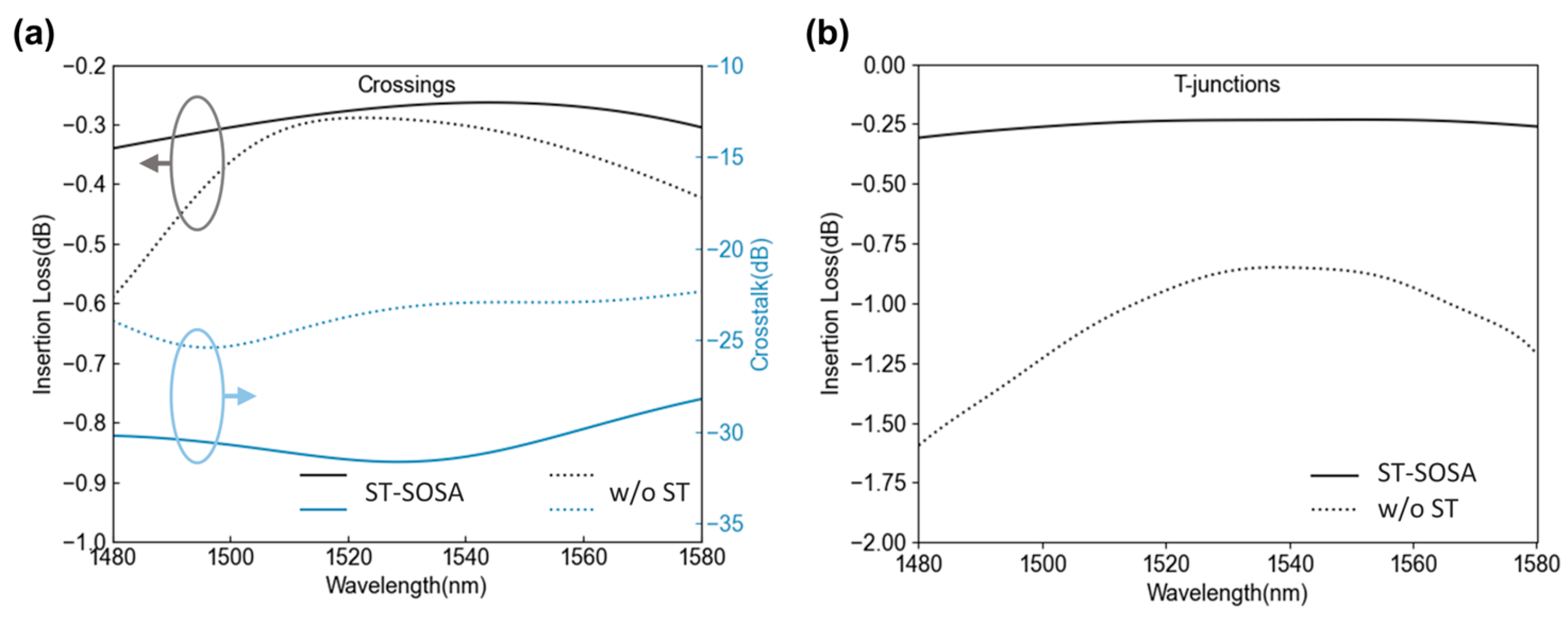
3.3. Broadband Performance Verification and Fabrication Tolerance Simulation

In order to achieve moderate broadband performance, broadband optimizations [26] (from 1480 nm to 1580 nm) were then implemented on the designed T-junction and crossing by simultaneously optimizing at wavelength points of 1505 nm, 1530 nm, and 1555 nm. Then, the three-dimensional finite-difference time-domain (3D FDTD) simulations were used to verify the broadband performance of the two types of broadband-optimized devices with the commercial software Lumerical FDTD. As a control group, broadband optimizations and verification were also implemented on T-junction and crossing designed using the general inverse design method (w/o ST-SOSA). The simulation results are illustrated in Figure 11, with key performance metrics summarized in Table 1. Through ST-SOSA, the ILs of the two devices reduced over the wavelength range of 1480–1580 nm, where the maximum IL of the T-junction (90° crossing) reduced from 1.6 dB (0.59 dB) to 0.31 dB (0.34 dB). The maximum CT of the 90° crossing reduced from −25.42 dB to −31.65 dB.
Then, the fabrication tolerance simulation was implemented to verify the fabrication robustness of the devices with and without ST-SOSA. Here, the deviations of the boundaries of the structure, which may have resulted from the under/over-etched errors in the fabrication process, were simulated and discussed. The structures of both devices with ST-SOSA and without ST-SOSA (the control group) were gradually dilated and eroded from 4 nm to 16 nm in a uniform step of 4 nm and simulated, respectively. The variations in the optical performance caused by such errors for the devices are shown in Figure 12 in error-bar form. To provide a more intuitive comparison, the simulation results are all shown in linear units instead of logarithmic units, as in Figure 11. The dashed lines in Figure 12 represent the performance of the designed devices with ST-SOSA (red lines) and without ST-SOSA (gray lines) with no error. The vertical solid lines are error bars that represent the maximum upper and lower deviations of the performance of the devices with respect to the degrees of dilated/eroded errors at several sample wavelength points. As can be seen in Figure 12a–c, the lengths of the error bars for the performance of the two devices with ST-SOSA are all shorter than those of the devices without ST-SOSA in the entire simulated wavelength range. The results obviously verified that through ST-SOSA, the devices were much less sensitive to the dilated/eroded errors and had better robustness against the impact of the fabrication uncertainty of under/over-etched errors. The Mean Absolute Errors (MAEs) of the simulated transmissions for all of the error-predicted structures relative to the designed structures were calculated and are listed in Table 1 to quantitatively analyze the fabrication robustness of the devices with ST-SOSA. Compared with the devices without ST-SOSA, the MAEs of the transmissions for the T-junction and crossing with ST-SOSA were reduced by 93% and 65%, respectively.

4. Conclusions

We propose a new SA method that effectively simplifies device structures according to their structural sensitivity to optical performance, termed SOSA, for inverse-designed nanophotonic devices. A modified structure transformation technique is proposed by introducing SOSA as a preliminary step in the original ST, termed ST-SOSA. ST-SOSA facilitates an overall simplification of the structures of inverse-designed devices rather than merely locally imposing geometric constraints. By transforming the complex structure of inverse-designed devices into simpler structures, ST-SOSA enhances the robustness of the devices against fabrication errors, without sacrificing their optical performance.
Two devices (90° crossing and T-junction) were demonstratively designed using the general inverse design method and then transformed using ST-SOSA. The new 90° crossing and T-junction were realized within three and four rounds of optimization, which is significantly fewer than the number of rounds required by the original ST technique. Through ST-SOSA, the simulated maximum IL, in the wavelength of 1480–1580 nm, of the T-junction (90° crossing) reduced from 1.6 dB (0.59 dB) to 0.31 dB (0.34 dB). The maximum crosstalk of the 90° crossing reduced from −25.42 dB to −31.65 dB. Finally, the fabrication tolerance simulation was implemented and the MAEs of the transmissions for error-predicted structures relative to the designed structures were calculated to quantitatively analyze the fabrication robustness of the devices. Compared with the devices without ST-SOSA, the MAEs of the transmissions for the T-junction and crossing with ST-SOSA were reduced by 93% and 65%, respectively, verifying that the devices with ST-SOSA are more robust to over/under-etching errors than those without ST-SOSA. The ST-SOSA technique is a flexible framework and allows for the incorporation of methods shown in recent works [5,8,27], improving the fabrication robustness in any of the OPO stages of the technique, to ensure that the designed structures can fulfill the more rigorous requirements of fabrication.

Supplementary Materials

The following supporting information can be downloaded at: https://www.mdpi.com/article/10.3390/photonics11030265/s1, Equations (S1)–(S4); Figure S1: The complete optimization process for the 90° crossings using ST-SOSA and the original ST; Figure S2: The complete optimization process for the T-junctions using ST-SOSA and the original ST.

Author Contributions

Conceptualization, Y.C; methodology, Y.C.; validation, Y.C.; investigation, Y.C., Z.D. and L.W. (Lihang Wang); resources, Y.C., J.Q. and J.W.; data curation, Y.C. and L.W. (Lan Wu); writing—original draft preparation, Y.C.; writing—review and editing, Y.C., J.Q., Z.D. and S.J.; visualization, Y.C.; supervision, J.Q., H.G. and J.W. All authors have read and agreed to the published version of the manuscript.

Funding

This work was partly supported by the Project: National Nature Science Foundation of China program (62275029, 61935003 and 62021005).

Institutional Review Board Statement

Not applicable.

Informed Consent Statement

Not applicable.

Data Availability Statement

Data are contained within the article.

Conflicts of Interest

The authors declare no conflicts of interest.

References

  1. Huang, J.; Ma, H.; Chen, D.; Yuan, H.; Zhang, J.; Li, Z.; Han, J.; Wu, J.; Yang, J. Digital nanophotonics: The highway to the integration of subwavelength-scale photonics Ultra-compact, multi-function nanophotonic design based on computational inverse design. Nanophotonics 2021, 10, 1011–1030. [Google Scholar] [CrossRef]
  2. Christiansen, R.E.; Sigmund, O. Inverse design in photonics by topology optimization: Tutorial. J. Opt. Soc. Am. B 2021, 38, 496–509. [Google Scholar] [CrossRef]
  3. Park, J.; Kim, S.; Nam, D.W.; Chung, H.; Park, C.Y.; Jang, M.S. Free-form optimization of nanophotonic devices: From classical methods to deep learning. Nanophotonics 2022, 11, 1809–1845. [Google Scholar] [CrossRef]
  4. Lazarov, B.; Wang, F.; Sigmund, O. Length scale and manufacturability in density-based topology optimization. Arch. Appl. Mech. 2016, 86, 189–218. [Google Scholar] [CrossRef]
  5. Hammond, A.M.; Oskooi, A.; Johnson, S.G.; Ralph, S.E. Photonic topology optimization with semiconductor-foundry design-rule constraints. Opt. Express 2021, 29, 23916–23938. [Google Scholar] [CrossRef] [PubMed]
  6. Guest, J.K.; Prevost, J.H.; Belytschko, T. Achieving minimum length scale in topology optimization using nodal design variables and projection functions. Int. J. Numer. Methods Eng. 2004, 61, 238–254. [Google Scholar] [CrossRef]
  7. Wang, F.W.; Lazarov, B.S.; Sigmund, O. On projection methods, convergence and robust formulations in topology optimization. Struct. Multidisc. Optim. 2011, 43, 767–784. [Google Scholar] [CrossRef]
  8. Vercruysse, D.; Sapra, N.V.; Su, L.; Trivedi, R.; Vučković, J. Analytical level set fabrication constraints for inverse design. Sci. Rep. 2019, 9, 8999. [Google Scholar] [CrossRef]
  9. Khoram, E.; Qian, X.P.; Yuan, M.; Yu, Z.F. Controlling the minimal feature sizes in adjoint optimization of nanophotonic devices using b-spline surfaces. Opt. Express 2020, 28, 7060–7069. [Google Scholar] [CrossRef]
  10. Chen, M.K.; Jiang, J.Q.; Fan, J.A. Design Space Reparameterization Enforces Hard Geometric Constraints in Inverse-Designed Nanophotonic Devices. ACS Photonics 2020, 7, 3141–3151. [Google Scholar] [CrossRef]
  11. Melati, D.; Dezfouli, M.K.; Grinberg, Y.; Schmid, J.H.; Cheriton, R.; Janz, S.; Cheben, P.; Xu, D.X. Design of Compact and Efficient Silicon Photonic Micro Antennas With Perfectly Vertical Emission. IEEE J. Sel. Top. Quantum Electron. 2021, 27, 8200110. [Google Scholar] [CrossRef]
  12. Schubert, M.F.; Cheung, A.K.C.; Williamson, I.A.D.; Spyra, A.; Alexander, D.H. Inverse Design of Photonic Devices with Strict Foundry Fabrication Constraints. ACS Photonics 2022, 9, 2327–2336. [Google Scholar] [CrossRef]
  13. Dong, Z.; Qiu, J.; Chen, Y.; Wang, L.; Guo, H.; Wu, J. Ultracompact and ultralow-loss S-bends with easy fabrication by numerical optimization. Opt. Lett. 2022, 47, 2434–2437. [Google Scholar] [CrossRef] [PubMed]
  14. Yu, Z.; Ma, Y.; Sun, X. Photonic welding points for arbitrary on-chip optical interconnects. Nanophotonics 2018, 7, 1679–1686. [Google Scholar] [CrossRef]
  15. Michaels, A.; Yablonovitch, E. Leveraging continuous material averaging for inverse electromagnetic design. Opt. Express 2018, 26, 31717–31737. [Google Scholar] [CrossRef] [PubMed]
  16. Yu, Z.; Feng, A.; Xi, X.; Sun, X. Inverse-designed low-loss and wideband polarization-insensitive silicon waveguide crossing. Opt. Lett. 2019, 44, 77–80. [Google Scholar] [CrossRef] [PubMed]
  17. Chen, Y.; Qiu, J.; Dong, Z.; Wang, L.; Liu, Y.; Guo, H.; Wu, J. Inverse Design of Free-Form Devices With Fabrication-Friendly Topologies Based on Structure Transformation. J. Light. Technol. 2023, 41, 4762–4776. [Google Scholar] [CrossRef]
  18. Li, C.; Xu, C.; Gui, C.; Fox, M.D. Distance Regularized Level Set Evolution and Its Application to Image Segmentation. IEEE Trans. Image Process. 2010, 19, 3243–3254. [Google Scholar] [CrossRef]
  19. Piggott, A.Y.; Lu, J.; Lagoudakis, K.G.; Petykiewicz, J.; Babinec, T.M.; Vučković, J. Inverse design and demonstration of a compact and broadband on-chip wavelength demultiplexer. Nat. Photonics 2015, 9, 374–377. [Google Scholar] [CrossRef]
  20. Piggott, A.Y.; Lu, J.; Babinec, T.M.; Lagoudakis, K.G.; Petykiewicz, J.; Vučković, J. Inverse design and implementation of a wavelength demultiplexing grating coupler. Sci. Rep. 2014, 4, 7210. [Google Scholar] [CrossRef]
  21. Lu, J. Maxwell-Solver [Source Code]. 2013. Available online: https://github.com/JesseLu/maxwell-solver (accessed on 1 March 2022).
  22. Chen, Y.; Ge, P.; Wang, G.; Weng, G.; Chen, H. An overview of intelligent image segmentation using active contour models. Intell. Robot. 2023, 3, 23–55. [Google Scholar] [CrossRef]
  23. Lu, H.; Li, Y.; Wang, Y.; Serikawa, S.; Chen, B.; Chang, C. Active Contours Model for Image Segmentation: A Review. In Proceedings of the 1st International Conference on Industrial Application Engineering 2013, Kitakyushu, Japan, 27–28 March 2013; pp. 104–111. [Google Scholar]
  24. Caselles, V.; Kimmel, R.; Sapiro, G. Geodesic Active Contours. Int. J. Comput. Vis. 1997, 22, 61–79. [Google Scholar] [CrossRef]
  25. Sapiro, G. Geometric Partial Differential Equations and Image Analysis; Cambridge University Press: Cambridge, UK, 2006. [Google Scholar]
  26. Piggott, A.Y.; Petykiewicz, J.; Su, L.; Vučković, J. Fabrication-constrained nanophotonic inverse design. Sci. Rep. 2017, 7, 1786. [Google Scholar] [CrossRef]
  27. Zhou, M.; Lazarov, B.S.; Wang, F.; Sigmund, O. Minimum length scale in topology optimization by geometric constraints. Comput. Methods Appl. Mech. Eng. 2015, 293, 266–282. [Google Scholar] [CrossRef]
Figure 1. The process of the proposed ST-SOSA for a 90° crossing. OPO: optical performance optimization, SOSA: sensitivity-oriented structure adjustment.
Photonics 11 00265 g001
Figure 2. Structural information of an inverse-designed 90° crossing and the result of curve evolution in ACM-DRLSE model. (a) The image representing the structure of an inverse-designed 90° crossing. (b) The edge indicator of the image in (a). (c) The LSF signifying the target boundary. (d) The zero-level contour of the LSF in (c).
Photonics 11 00265 g002
Figure 3. The non-linear mappings Wθ(S) of the structural sensitivity S with different θ.
Photonics 11 00265 g003
Figure 4. Structural information of an inverse-designed 90° crossing and the result of curve evolution in SOSA with θ = 7 / 5 (a) The structural sensitivity (in a logarithmic scale). (b) The weighted edge indicator. (c) The LSF after evolution in the proposed modified ACM-DRLSE model. (d) The zero-level contour of the LSF in (c).
Photonics 11 00265 g004
Figure 5. The process of the SOSA-OPO for a 90° crossing. (a) The weighted edge indicator defined with different θ . The boundaries 𝒞θ (b) of the adjusted structures (c) after SOSA. (d) The OPO-optimized structures ϕ θ * with the initial structures ϕ ˜ θ .
Photonics 11 00265 g005
Figure 6. The boundary reductions and the objective function values of 90° crossings with respect to different θ . Black dashed line indicates the percentage reduction in the boundary of ϕ θ * compared to the boundary of ϕ * . Blue dashed line indicates (in a logarithmic scale) after SOSA-OPO. Gray horizontal dashed line indicates of the local optimal value before SOSA.
Photonics 11 00265 g006
Figure 7. The complete optimization process for the 90° crossing using ST-SOSA. (a) (in a logarithmic scale) in OPOs during ST-SOSA. The gray vertical dashed lines indicate connectors between two adjacent OPOs: specifically, SOSA between the first two OPOs is indicated by the red upward arrow. (b) Top view of the structure of the 90° crossing and corresponding electric field intensity (normalized) obtained in each OPO.
Photonics 11 00265 g007
Figure 8. The process of the SOSA-OPO for a T-junction. (a) The initial structure of the T-junction. (b) The structure of the inverse-designed T-junction and (c) its structural sensitivity (in a logarithmic scale). (d) The adjusted structures after SOSA with different θ . (e) The structures ϕ θ * obtained after a new round of OPO with initial structures ϕ ˜ θ , and the corresponding electric field intensity (normalized).
Photonics 11 00265 g008
Figure 9. The boundary reductions and the objective function values of T-junctions with different θ . Black dashed line indicates the percentage reduction in the boundary of ϕ θ * compared with the boundary of ϕ * . Blue dashed line indicates (in a logarithmic scale) after SOSA-OPO. Gray horizontal dashed line indicates of the local optimal value before SOSA.
Photonics 11 00265 g009
Figure 10. The complete optimization process for the T-junction using ST-SOSA. (a) (in a logarithmic scale) in OPOs during ST-SOSA. The gray vertical dashed lines indicate connectors between two adjacent OPOs; specifically, SOSA between the first two OPOs is indicated by the red upward arrow. (b) Top view of the structure of the 90° crossing and corresponding electric field intensity (normalized) obtained in each OPO.
Photonics 11 00265 g010
Figure 11. The simulation results of the broadband (a) 90° crossings and (b) T−junctions designed with ST-SOSA and without ST-SOSA.
Photonics 11 00265 g011
Figure 12. The performance variations caused by dilated/eroded errors in degrees of 4–16 nm for the devices with ST-SOSA (vertical red lines) and devices without ST-SOSA (vertical gray lines). Dashed lines: The performance of the designed devices with no error. (a) The transmission deviations of the T-junctions. (b,c) The transmission and crosstalk deviations of 90° crossings.
Photonics 11 00265 g012
Table 1. Simulation results of the designed devices.
DevicesT-JunctionsCrossings
MethodsST-SOSAw/o STST-SOSAw/o ST
IL (dB) @ 1530 nm0.230.870.270.29
Max IL (dB)0.311.600.340.59
MAE of Transmission0.0130.1850.0170.049
CT (dB) @ 1530 nm--−31.65−23.20
Max CT (dB)--−31.65−25.42
Disclaimer/Publisher’s Note: The statements, opinions and data contained in all publications are solely those of the individual author(s) and contributor(s) and not of MDPI and/or the editor(s). MDPI and/or the editor(s) disclaim responsibility for any injury to people or property resulting from any ideas, methods, instructions or products referred to in the content.

