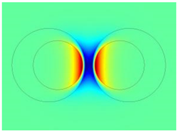
Article

Surface Plasmon Waveguide Based on Nested Dielectric Parallel Nanowire Pairs Coated with Graphene

by
Lixia Yu
1,*,
Ji Liu
1 and
Wenrui Xue
2
1
School of Information and Communication Engineering, North University of China, Taiyuan 030051, China
2
College of Physics and Electronic Engineering, Shanxi University, Taiyuan 030006, China
*
Author to whom correspondence should be addressed.
Photonics 2024, 11(5), 441; https://doi.org/10.3390/photonics11050441
Submission received: 19 April 2024 / Revised: 29 April 2024 / Accepted: 7 May 2024 / Published: 9 May 2024
(This article belongs to the Special Issue Design and Applications of Novel Nanophotonics Devices)

Abstract

:
A kind of surface plasmon waveguide composed of two nested cylindrical dielectric parallel nanowire pairs coated with graphene was designed and studied. The dependence of the mode characteristics and the normalized gradient force of the lowest two modes supported by the waveguide on the parameters involved were analyzed by using the multipole method. To ensure rigor, the finite element method was employed to verify the accuracy of the multipole method, thus confirming its results. The results show that the multipole method is a powerful tool for handling this type of waveguide. The real part of the effective refractive index, the propagation length, the figure of merit, and the normalized gradient force can be significantly affected by the operating wavelength, the Fermi energy of graphene, the waveguide geometric parameters, and the refractive index of the inner dielectric nanowire. Due to the employment of nested dielectric nanowire pairs coated with graphene, this waveguide structure exhibits significant gradient force that surpasses 100 nN·μm−1·mW−1. The observed phenomena can be attributed to the interaction of the field with graphene. This waveguide holds promising potential for applications in micro/nano integration, optical tweezers, and sensing technologies.

1. Introduction

Surface plasmon polaritons (SPPs) are electromagnetic modes that arise at the metal-dielectric interface through the interaction of free electrons and photons [1]. Thanks to their ability to transcend the diffraction limit and possess robust local field enhancement properties, SPPs offer immense potential for applications in nanoscale optical information transmission and processing [2], ultra-sensitive biological detection [3], sensing [4], and novel light sources [5].
Surface plasmon waveguides (SPWs) are devices that guide the propagation of SPPs [6]. The materials used to construct SPWs include noble metals [7], semiconductors [8], and two-dimensional materials such as molybdenum disulfide [9] and graphene [10]. The typical structures of SPWs are strip type [11,12], slot type [13,14], wedge type [15,16], channel type [16,17], hybrid type [18], etc.
In the infrared-to-terahertz frequency regime, graphene has properties similar to metals, and SPPs can be excited on its surface. Graphene-coated dielectric nanowires are a new type of surface plasmon waveguide that emerged in recent years [19]. A cylindrical dielectric nanowire coated with single-layer graphene was designed by Y. Gao et al. The authors obtained a dispersion relationship of modes using a semi-analytical method, and the low-order modes supported by this waveguide were characterized [20,21]. J.-P. Liu and his colleagues devised a cylindrical dielectric nanowire featuring a double-layer structure clad in single-layer graphene. Employing the finite-difference time-domain method, they examined the low-order mode sustained by this waveguide. Furthermore, they highlighted that mode properties can be fine-tuned by varying the waveguide’s geometric factors and graphene’s Fermi energy, as referenced in [22]. Research findings pertaining to cylindrical dielectric nanowires, utilizing a double-layer graphene structure, reveal that factors such as the Fermi energy of graphene, the separation between its inner and outer layers, and the radius of the dielectric nanowires within the core region significantly influence modal behavior [23]. Notably, it has been demonstrated that the inherent tradeoff between mode confinement and propagation loss can be overcome [24]. Furthermore, the long-range SPP (LRSPP) mode exhibits both an extended propagation length and deep subwavelength constraints, marking a significant advancement in the field [25]. R. Xing and his team designed a cylindrical dielectric nanowire that was coated with multiple layers of graphene. The results indicate that this waveguide has a stronger confinement ability on the field than a nanowire waveguide coated with graphene with the same outer diameter [26]. The results of research on graphene-coated dielectric nanowires with substrates show that radiation leakage to the substrate can be effectively suppressed by the introduced buffer layer [27], the deep subwavelength plasmon mode with ultra-low loss can be supported [28], and a longer propagation length and a smaller mode area can be obtained simultaneously [29]. The characteristics of the six lowest-order surface plasmon modes have been studied [30]. A dual-multilayer nanoring waveguide configuration was introduced, and both surface plasmon modes and the augmentation of the gap field within the intervening space between these waveguides were examined [31]. S. Ye et al.’s research on graphene-coated hexagonal boron nitride nanowire pairs shows that this waveguide supports both the plasmon phonon polarization (SPP-HP) mode and the phonon polarization (PHP) mode [32]. The findings of research on dielectric nanowire pairs coated with graphene and equipped with a substrate reveal that mode characteristics can be efficiently tailored by altering the thickness of the substrate, as reported in [33]. Inserting a low-refractive index material layer between the nanowire and the substrate can compensate for the accompanying loss of the substrate, so that the mode’s characteristics can be adjusted to achieve better performance [34].
Optical forces play an essential role in small-particle manipulations with broad applications in biology, chemistry, and physics [35,36,37,38,39,40,41]. It has been demonstrated that, in comparison to plasmonic metal-coated nanowire systems, the unique properties of graphene plasmons (GPs) enable significantly greater field enhancement, and the gradient force between the two nanowires can be as high as 20 nN·μm−1·mW−1 [30]. Therefore, it is reasonable to expect the existence of a strong gradient force within nanowire systems coated with graphene that are coupled together.
Our team’s investigation into nested dielectric nanowire waveguides coated with single-layer graphene on both inner and outer surfaces has uncovered fascinating results. We found that the three lowest modes—mode 0, mode 1, and mode 2—can be effectively combined using the zero-order mode or/and the first-order modes of two individual nanowires. Notably, mode 0 exhibits a superior figure of merit and the most optimal performance among these modes within the relevant parameter range. Furthermore, the characteristics of these modes can be tailored by adjusting the waveguide’s parameters, the working wavelength, and the Fermi energy of graphene [42,43].
Based on our previous work [43], here, we designed a new type of waveguide composed of nested dielectric parallel nanowire pairs coated with graphene. To our knowledge, this type of eccentric nested dielectric parallel nanowire pairs coated with graphene has not been studied previously. Using the multipole method (MPM), the dependence of the mode characteristics of the two lowest-order modes of this kind of waveguide on the operating wavelength, the Fermi energy of graphene, the geometric parameters, and the refractive index of the inner dielectric nanowire were analyzed. This type of waveguide has broad application prospects in fields such as micro/nano integration, optical tweezers, and sensing [44,45].
The content of this paper is arranged as follows: in the second part, the structure model and calculation method will be introduced in detail. The third part is the results and discussion. A detailed discussion is conducted on the phenomenon and reasons why the mode characteristics of two modes vary with the working wavelength, the Fermi energy of graphene, the geometric parameters, and the refractive index of the inner dielectric nanowire. The last part is the summary.

2. Waveguide Structure and Calculation Method

The waveguide structure presented in this paper is depicted in Figure 1 and consists of four nested cylindrical dielectric parallel nanowires coated with graphene. The radii of the cylindrical nanowires are ρ 10 , ρ 20 , ρ 30 , and ρ 40 , respectively. Assume that the minimum distance between the surface of the embedded cylindrical nanowire and the surface of the parent cylindrical nanowire is s and the minimum distance between the outer surfaces of two parallel nanowires is d . The surfaces of the four cylindrical nanowires are coated with a single layer of graphene material, and the surface conductivity is σ g . The refractive indices of the dielectrics in region I, region II, region III, and region IV are n 1 , n 2 , n 3 , and n 4 , respectively. Region V is the air background with a refractive index of n 0 = 1.0 .
We use the multipole method to analyze the mode characteristics supported by this waveguide. The symmetric center o i of the cylindrical nanowire is taken as the origin to establish a rectangular coordinate system o i x i y i and a polar coordinate system o i ρ i ϕ i . Here, i = 1, 2, 3, and 4 correspond to the four cylindrical nanowires shown in Figure 1, respectively. Assuming that the four cylindrical nanowires exist separately, the distribution of the E z and H z fields in their respective coordinate systems can be expanded into series. For example, for the first dielectric cylinder, they are as follows:
Inside the 1st cylindrical nanowire:
E z 11 ( ρ 1 , ϕ 1 ) = m = 0 A m I m ( λ 1 ρ 1 ) cos ( m ϕ 1 ) + m = 1 A m I m ( λ 1 ρ 1 ) sin ( m ϕ 1 )
H z 11 ( ρ 1 , ϕ 1 ) = m = 0 B m I m ( λ 1 ρ 1 ) cos ( m ϕ 1 ) + m = 1 B m I m ( λ 1 ρ 1 ) sin ( m ϕ 1 )
Outside the 1st cylindrical nanowire:
E z 12 ( ρ 1 , ϕ 1 ) = m = 0 C m K m ( λ 2 ρ 1 ) cos ( m ϕ 1 ) + m = 1 C m K m ( λ 2 ρ 1 ) sin ( m ϕ 1 )
H z 12 ( ρ 1 , ϕ 1 ) = m = 0 D m K m ( λ 2 ρ 1 ) cos ( m ϕ 1 ) + m = 1 D m K m ( λ 2 ρ 1 ) sin ( m ϕ 1 )
Here, I m and K m are Bessel functions of order m, and A m , A m , B m , and B m are undetermined coefficients of order m. λ 1 = β 2 ω 2 ε 1 ε 0 μ 0 , λ 2 = β 2 ω 2 ε 2 ε 0 μ 0 . β is the propagation constant, ε 1 = n 1 2 , ε 2 = n 2 2 , ε 0 is the dielectric constant in vacuum, and μ 0 is the permeability in vacuum.
Utilizing the superposition principle of fields, the E z and H z field distributions can be derived individually in regions I, II, III, IV, and V. For example, in region I:
( E z ) I = E z 11 ( ρ 1 , ϕ 1 ) + E z 21 ( ρ 2 , ϕ 2 ) + E z 32 ( ρ 3 , ϕ 3 ) + E z 42 ( ρ 4 , ϕ 4 )
( H z ) I = H z 11 ( ρ 1 , ϕ 1 ) + H z 21 ( ρ 2 , ϕ 2 ) + H z 32 ( ρ 3 , ϕ 3 ) + H z 42 ( ρ 4 , ϕ 4 )
Here, E z 21 ( ρ 2 , ϕ 2 ) and H z 21 ( ρ 2 , ϕ 2 ) are the z component of the electric field strength and magnetic field strength inside the 2nd cylindrical nanowire, respectively. E z 32 ( ρ 3 , ϕ 3 ) and H z 32 ( ρ 3 , ϕ 3 ) are the z component of the electric field strength and magnetic field strength outside the 3rd cylindrical nanowire. E z 42 ( ρ 4 , ϕ 4 ) and H z 42 ( ρ 4 , ϕ 4 ) are the z component of the electric field strength and magnetic field strength outside the 4th cylindrical nanowire.
The distribution of transverse fields ( E ρ ) i , ( H ρ ) i , ( E ϕ ) i , and ( H ϕ ) i in regions i can be obtained by using the relationship between the transverse and longitudinal components of fields. Here i = I, II, III, IV, and V. For example,
( E ϕ ) I = 1 λ 1 2 { ( j β ) 1 ρ 1 [ m = 0 A m I m ( λ 1 ρ 1 ) ( m ) sin ( m ϕ 1 ) + m = 0 A m I m ( λ 1 ρ 1 ) ( m ) cos ( m ϕ 1 )    + ϕ 1 [ m = 0 E m I m ( λ 2 ρ 2 ) cos ( m ϕ 2 ) + m = 1 E m I m ( λ 2 ρ 2 ) sin ( m ϕ 2 ) ]    + ϕ 1 [ m = 0 R m K m ( λ 2 ρ 3 ) cos ( m ϕ 3 ) + m = 1 R m K m ( λ 2 ρ 3 ) sin ( m ϕ 3 ) ]    + ϕ 1 [ m = 0 V m K m ( λ 0 ρ 4 ) cos ( m ϕ 2 ) + m = 1 V m K m ( λ 0 ρ 4 ) sin ( m ϕ 4 ) ] ] + ( j ω μ 0 ) [ m = 0 B m ( λ 1 ) I m ( λ 1 ρ 1 ) cos ( m ϕ 1 ) + m = 0 B m ( λ 1 ) I m ( λ 1 ρ 1 ) sin ( m ϕ 1 )    + ρ 1 [ m = 0 F m I m ( λ 2 ρ 2 ) cos ( m ϕ 2 ) + m = 1 F m I m ( λ 2 ρ 2 ) sin ( m ϕ 2 ) ]    + ρ 1 [ m = 0 S m K m ( λ 2 ρ 3 ) cos ( m ϕ 3 ) + m = 1 S m K m ( λ 2 ρ 3 ) sin ( m ϕ 3 ) ]    + ρ 1 [ m = 0 W m K m ( λ 0 ρ 4 ) cos ( m ϕ 4 ) + m = 1 W m K m ( λ 0 ρ 4 ) sin ( m ϕ 4 ) ] ] }
Here, E m and E m are undetermined coefficients of field E z 21 inside the 2nd cylindrical nanowire, F m and F m are undetermined coefficients of field H z 21 inside the 2nd cylindrical nanowire, R m and R m are undetermined coefficients of field E z 32 outside the 3rd cylindrical nanowire, S m and S m are undetermined coefficients of field H z 32 outside the 3rd cylindrical nanowire, V m and V m are undetermined coefficients of field E z 42 outside the 4th cylindrical nanowire, and W m and W m are undetermined coefficients of field H z 42 outside the 4th cylindrical nanowire, λ 0 = β 2 ω 2 ε 0 μ 0 .
The derivatives involved in the above formula can be obtained by the point product of the gradient of a scalar field and the unit vector of the polar coordinate system. For example,
ψ ( ρ 2 , ϕ 2 ) ρ 1 = ψ ( ρ 2 , ϕ 2 ) · ρ ^ 1 = ψ ( ρ 2 , ϕ 2 ) ρ 2 ρ ^ 2 · ρ ^ 1 + ψ ( ρ 2 , ϕ 2 ) ρ 2 ϕ 2 ϕ ^ 2 · ρ ^ 1
ψ ( ρ 2 , ϕ 2 ) ρ 1 ϕ 1 = ψ ( ρ 2 , ϕ 2 ) · ϕ ^ 1 = ψ ( ρ 2 , ϕ 2 ) ρ 2 ρ ^ 2 · ϕ ^ 1 + ψ ( ρ 2 , ϕ 2 ) ρ 2 ϕ 2 ϕ ^ 2 · ϕ ^ 1
Here, ψ ( ρ 2 , ϕ 2 ) represents any function with ρ 2 and ϕ 2 as variables, such as I m ( λ 2 ρ 2 ) cos ( m ϕ 2 ) . ρ ^ 1 and ϕ ^ 1 represent the two unit vectors in the polar coordinate system o 1 ρ 1 ϕ 1 , while ρ ^ 2 and ϕ ^ 2 represent the two unit vectors in the polar coordinate system o 2 ρ 2 ϕ 2 .
The boundary value relation of the tangential field applies at the four interfaces which are located at ρ 10 , ρ 20 , ρ 30 , and ρ 40 , respectively. For example, at the interface of ρ 10 ,
( E z ) I | ρ 10 = ( E z ) II | ρ 10
( E ϕ ) I | ρ 10 = ( E ϕ ) II | ρ 10
( H z ) I | ρ 10 ( H z ) II | ρ 10 = σ g ( E ϕ ) I | ρ 10
( H ϕ ) I | ρ 10 ( H ϕ ) II | ρ 10 = σ g ( E z ) I | ρ 10
Here, σ g is the conductivity of graphene, which is obtained from the Cooper formula [46].
From the given formula, we can derive a system of linear algebraic equations:
[ a m n ( 0 , 0 ) a m n ( 0 , 1 ) a m n ( 0 , 31 ) a m n ( 1 , 0 ) a m n ( 1 , 1 ) a m n ( 1 , 31 ) a m n ( 15 , 0 ) a m n ( 15 , 1 ) a m n ( 15 , 31 ) ] [ [ A ] [ A ] [ H ] ] = 0
Here, [ A ] is the column vector composed of undetermined coefficients A 0 , A 1 , and A M 1 . In order to perform calculations on a computer, the infinite series shown in Formulas (1)–(4) must be truncated. Here, M is the maximum value of m . To ensure that the coefficient matrix in formula (14) is a square matrix, the maximum value of n must be 2 M . [ A ] , [ B ] , and [ H ] are constructed in the same way. a m n ( i , j ) is the submatrix of m × n , for example,
a m n ( 0 , 0 ) = I m ( λ 1 ρ 10 ) cos ( m ϕ 1 n )
We found that as M gradually increases, calculation accuracy will gradually improve. When M = 15, the results obtained by the multipole method are very close to those obtained by the finite element method, and the relative error can reach the order of 10−4. In the following calculations, we take M = 15.
Solving the linear algebraic equations (14) by the singular value decomposition (SVD) method [47], the characteristics of each mode can be obtained, including the field distribution, the real part of the effective refractive index R e ( n e f f ) , which describes the amount of phase delay per unit length in the waveguide relative to the phase delay per unit length in vacuum [48], and the imaginary part of the effective refractive index I m ( n e f f ) ,which describes the loss of the waveguide structure [48]. Then, propagation length L p r o p and the figure of merit ( F O M ) can be obtained: L p r o p = λ / { 4 π I m ( n e f f ) } [49], F O M = R e ( n e f f ) / I m ( n e f f ) [50]. Here, L p r o p is used to describe the propagation distance, and F O M is used to describe the quality of the modes. The gradient force along the x direction is evaluated by F x = [ Σ T · d σ ] · e ^ x ; here, T is the Maxwell Stress Tensor (MST), Σ is an arbitrary surface enclosing the left or the right nested cylindrical dielectric parallel nanowires, and e ^ x is the unit vector along the x direction. The component of T here is T α β = ε E α E β + μ H α H β 1 2 δ α β ( ε E 2 + μ H 2 ) , where δ is the Kronecker delta function [51]. For the convenience of calculation, the gradient force F x is normalized to f x by the power along z direction, f x = F x / Σ S z d x d y , where S z is the energy flow density component along the z direction of the mode and Σ is the cross-section of the left or the right nested cylindrical dielectric parallel nanowire waveguide.

3. Results and Discussion

In this section, the synthesis of the two lowest-order modes supported by wave-guides is initially explored. Subsequently, the discussion focuses on how these modes’ R e ( n e f f ) , L p r o p , F O M , and f x vary with factors such as the working wavelength, the Fermi energy of graphene, the radii of embedded and parent cylindrical nanowires, and the minimum distances between the outer surfaces of parallel nanowires and between the surfaces of embedded and parent cylinders. For the sake of structural symmetry, it is assumed that the radii of two embedded cylindrical nanowires are the same, and the radii of the two parent cylindrical nanowires are also the same, i.e., ρ 10 = ρ 30 , ρ 20 = ρ 40 . The refractive indices of region I and region III are the same, while the refractive indices of region II and region IV are the same, i.e., n 1 = n 3 , n 2 = n 4 . To verify the accuracy of the multipole method, we also provide the results obtained by the finite element method. In the figures in Section 3.2, Section 3.3, Section 3.4, Section 3.5, Section 3.6, Section 3.7 and Section 3.8, solid lines represent the results obtained by the multipole method, and dotted lines represent the results obtained by the finite element method.

3.1. The Two Lowest-Order Modes

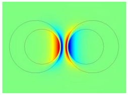
The waveguide shown in Figure 1 supports many modes. Table 1 shows the two lowest-order modes, namely, the combination of mode 0 and mode 1, the distribution of electric field z component, and the distribution of electric field intensity. From Table 1, it can be seen that mode 0 and mode 1 are combined by zero-order modes supported by a single nanowire [20,21]. The E z field distribution of mode 0 is symmetric about the x-axis and antisymmetric about the y-axis, while the E z field distribution of mode 1 is symmetric about both the x-axis and y-axis. Because the fields of these two modes are mainly concentrated in the gap area between the left and right embedded nanowires, they have a certain practical value, while the field distribution of other higher-order modes will diffuse to the entire range of the waveguide, which is less practical. Therefore, in the following text, we will only discuss the mode characteristics of the two lowest-order modes.

3.2. Influence of the Working Wavelength on Mode Characteristics

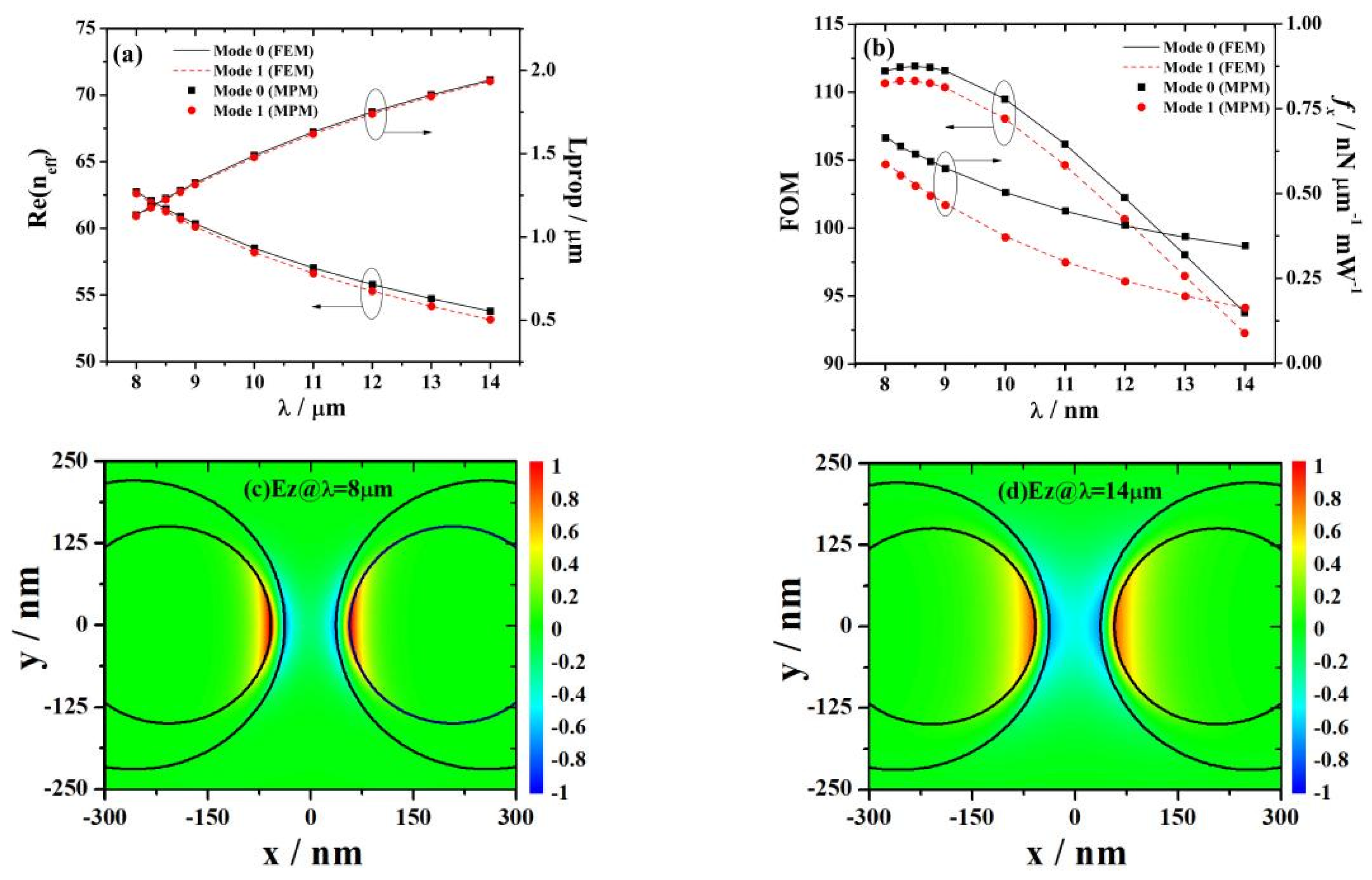
Under the conditions of E f = 0.5 eV, ρ 10 = ρ 30 = 150 nm, ρ 20 = ρ 40 = 220 nm, s = 20 nm, d = 75 nm, n 1 = n 3 = 1.45, and n 2 = n 4 = 1.45, the relationship of the real part of the effective refractive index, propagation length, figure of merit, and normalized gradient force of the two modes with wavelength is shown in Figure 2a,b. It can be seen that in the wavelength range of 8–14 microns, as the wavelength increases, the R e ( n e f f ) of both modes monotonically decreases. Mode 0 has a slower descent speed, while mode 1 has a faster descent speed. The L p r o p of the two modes shows a monotonic growth trend. The propagation distance of mode 0 and mode 1 is almost the same. F O M shows a trend of first increasing and then decreasing. Under certain wavelength conditions, mode 0 has a higher figure of merit and mode 1 has a lower figure of merit. The magnitude of the normalized gradient force f x shows a monotonic decreasing trend. Mode 0 has a slower descent speed, while mode 1 has a faster descent speed. The above phenomenon can be explained by the fact that different wavelengths correspond to different field distributions of the mode. Figure 2c,d show the E z field distribution of mode 1 at wavelengths of 8 microns and 14 microns, respectively. Comparing the two figures, it becomes evident that as the wavelength decreases, the field becomes more confined to the graphene layer adjacent to the surfaces of the two nanowires. This confinement enhances the interaction between the field and the graphene, leading to increased losses, shorter propagation distances, and stronger gradient forces. Conversely, when the wavelength increases, the field diffuses more widely into the space separating the nanowires, weakening the interaction with the graphene. Consequently, there is reduced loss, a longer propagation distance, and a weaker gradient force.

3.3. Influence of the Fermi Energy of Graphene on Mode Characteristics

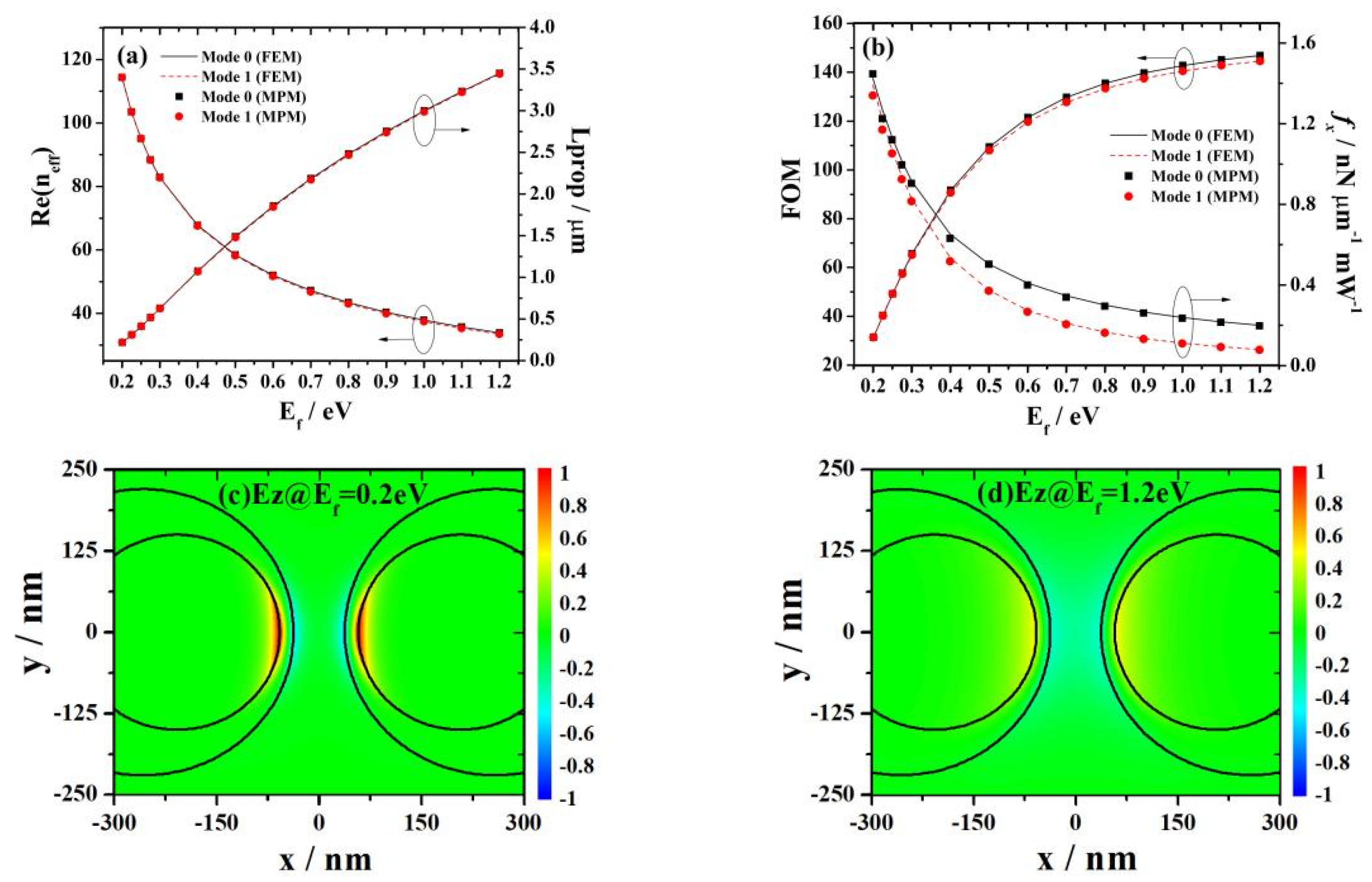
The relationship between the real part of the effective refractive index, propagation length, figure of merit, and normalized gradient force of the two modes with Fermi energy under the conditions of λ = 10 μ m , ρ 10 = ρ 30 = 150 nm, ρ 20 = ρ 40 = 220 nm, s = 20 nm, d = 75 nm, n 1 = n 3 = 1.45, and n 2 = n 4 = 1.45 is shown in Figure 3a,b. It can be seen that in the range of 0.2–1.2 eV, as the Fermi energy increases, the R e ( n e f f ) of both modes monotonically decreases. The descent speed of mode 0 is almost the same as that of mode 1. The L p r o p of both modes shows a monotonic growth trend. The propagation distance of mode 0 and mode 1 is almost the same. The F O M of both modes shows a monotonic growth trend. Under certain wavelength conditions, mode 0 has a higher figure of merit and mode 1 has a lower figure of merit. The magnitude of the normalized gradient force f x shows a monotonic decreasing trend. Mode 0 has a slower descent speed, while mode 1 has a faster descent speed. The above phenomenon can be explained by the fact that different Fermi energies correspond to different field distributions of the mode. The E z field distribution of mode 1 at Fermi energies of 0.2 eV and 1.2 eV are shown in Figure 3c,d. Comparing the two graphs, it becomes apparent that when the Fermi energy is low, the field is more concentrated within the graphene layer adjacent to the nanowire surface between the two nanowires. This strong interaction between the field and graphene leads to increased losses, shortened propagation distances, and a relatively large normalized gradient force. Conversely, at high Fermi energy, the field spreads out into the space between the nanowires, weakening the interaction with the graphene. Consequently, there are reduced losses, longer propagation distances, and a relatively smaller normalized gradient force.

3.4. Influence of the Radii of the First Nanowire on Mode Characteristics

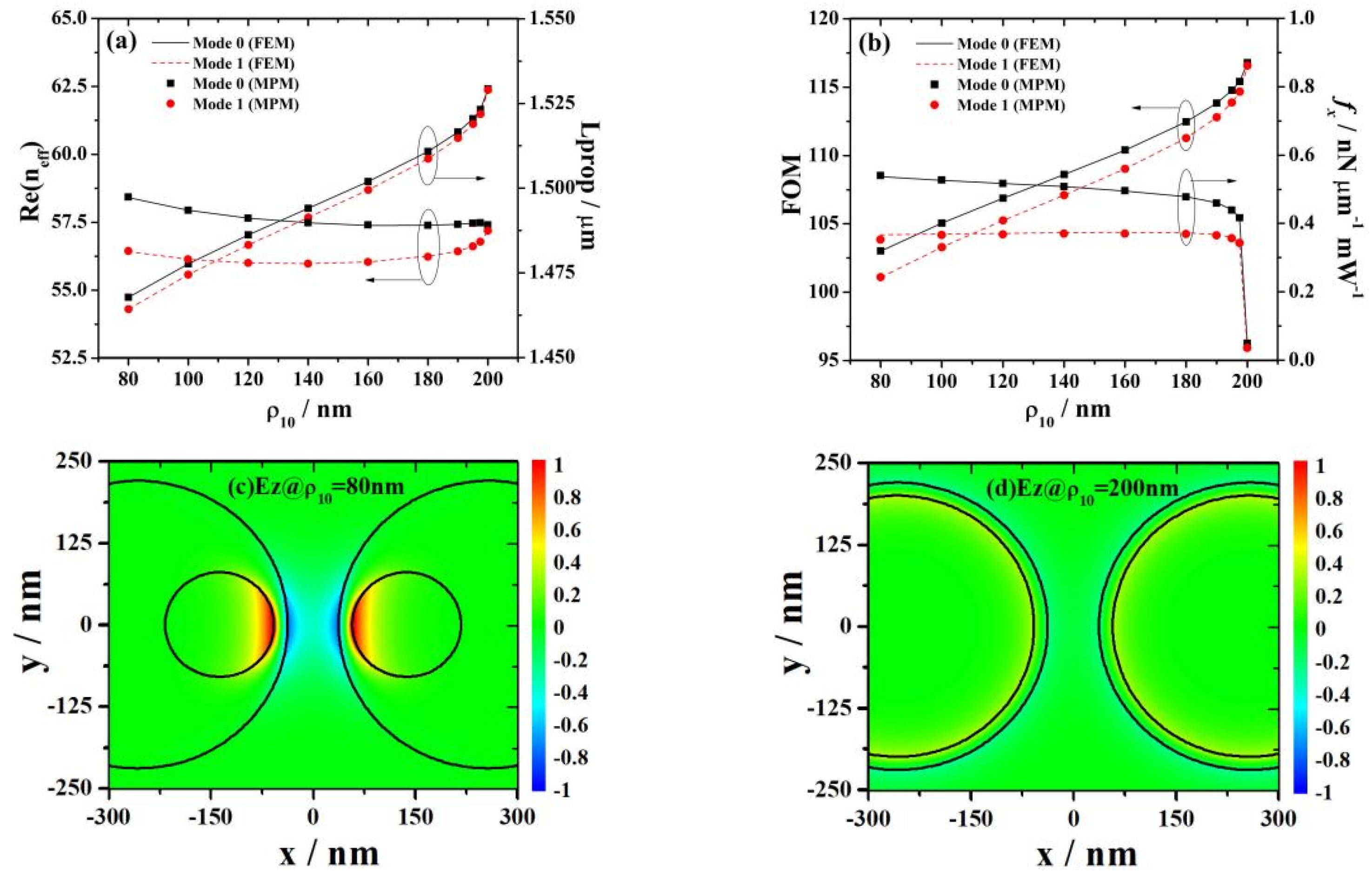
Under the conditions of λ = 10 μ m , E f = 0.5 eV, ρ 20 = ρ 40 = 220 nm, s = 20 nm, d = 75 nm, n 1 = n 3 = 1.45, and n 2 = n 4 = 1.45, the relationship between the real part of the effective refractive index, propagation length, figure of merit, and normalized gradient force of the two modes with the radius ρ 10 ( ρ 30 = ρ 10 ) of the embedded cylindrical nanowire are shown in Figure 4a,b. It can be seen that, in the range of 80–200 nm, as ρ 10 increases, the R e ( n e f f ) of both modes shows a trend of first decreasing and then increasing. The L p r o p of the two modes shows a monotonic upward trend. The F O M of both modes shows a monotonic growth trend. The magnitude of the normalized gradient force f x first shows a slow decreasing trend, and then shows a significant decreasing trend around 200 nm. When ρ 10 is small, the R e ( n e f f ) , L p r o p , F O M , and f x of mode 0 are all higher than the R e ( n e f f ) , L p r o p , F O M , and f x of mode 1. When ρ 10 approaches 200 nm, the embedded cylindrical nanowires and the parent cylindrical nanowires tend to be coaxial. At this point, the R e ( n e f f ) , L p r o p , F O M , and f x of both mode 0 and mode 1 tend to be consistent. The above phenomenon can be explained by the fact that different radii of embedded cylindrical nanowires correspond to different mode field distributions. The E z field distribution of mode 1 at ρ 10 = 80 nm and 200 nm are shown in Figure 4c,d, respectively. Comparing these two graphs, we observe that when ρ 10 is small, the field remains confined to the graphene layer close to the surface of the two nanowires. This leads to a strong interaction between the field and graphene, causing higher losses, shorter propagation distances, and a relatively larger normalized gradient force. However, when ρ 10 reaches 200 nm, field intensity weakens and distributes almost uniformly across the four graphene rings. Consequently, the interaction between the field and graphene becomes relatively weak, resulting in lower losses, longer propagation distances, and a smaller normalized gradient force.

3.5. Influence of the Radii of the Second Nanowire on Mode Characteristics

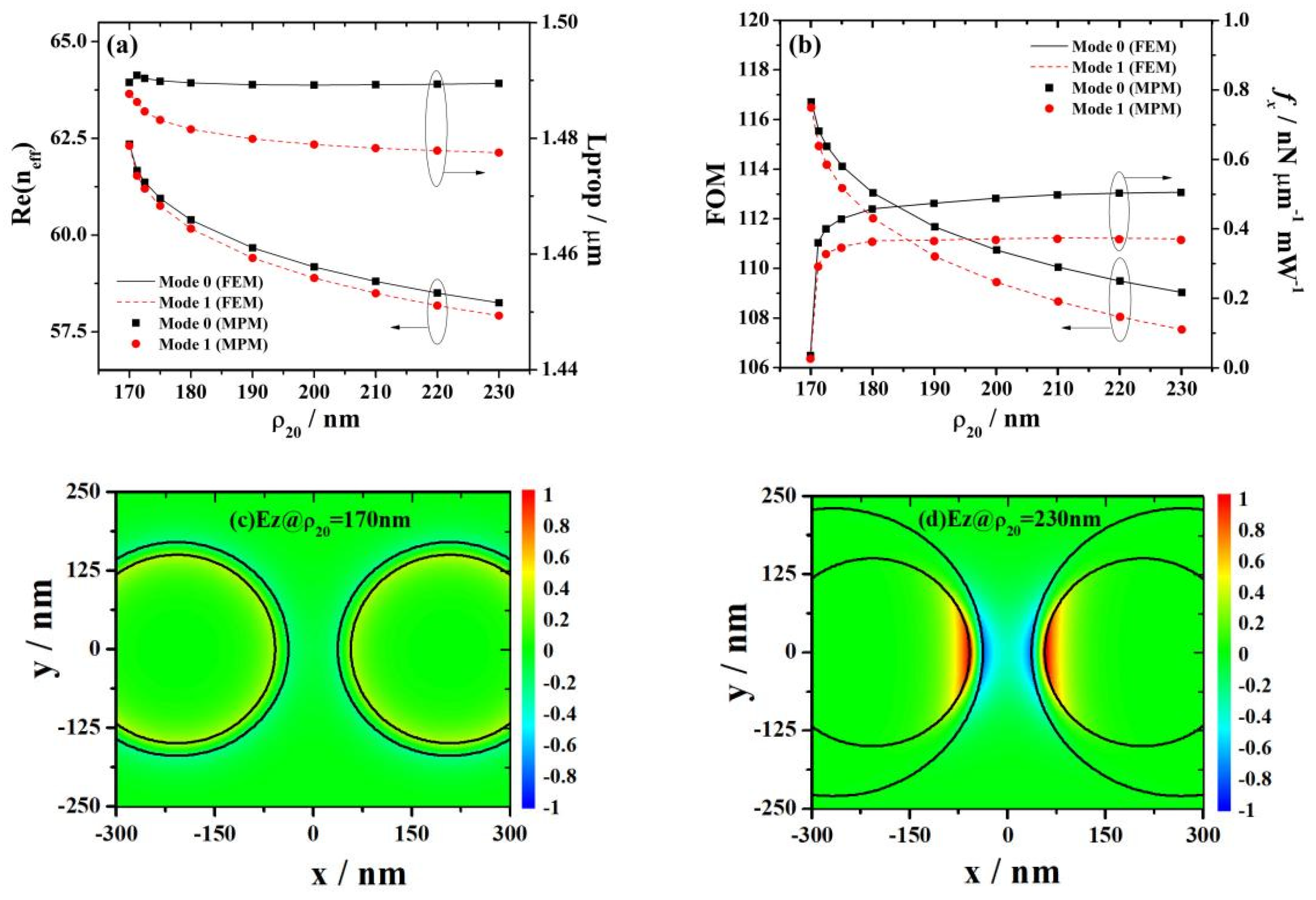
The relationship between the real part of the effective refractive index, propagation length, figure of merit, and normalized gradient force of the two modes with the radius of the parent cylindrical nanowire ρ 20 ( ρ 40 = ρ 20 ) under the conditions of λ = 10 μ m , E f = 0.5 eV, ρ 10 = ρ 30 = 150 nm, s = 20 nm, d = 75 nm, n 1 = n 3 = 1.45, and n 2 = n 4 = 1.45 is shown in Figure 5a,b. It can be seen that in the range of 170–230 nm, as ρ 20 increases, the R e ( n e f f ) , L p r o p , and F O M of the two modes all show a monotonic decreasing trend, while the normalized gradient force f x shows a monotonic increasing trend. When ρ 20 is large, the R e ( n e f f ) , L p r o p , F O M , and f x of mode 0 are all higher than the R e ( n e f f ) , L p r o p , F O M , and f x of mode 1. When ρ 20 approaches 170 nm, the embedded cylindrical nanowires and the parent cylindrical nanowires tend to be coaxial. At this time, the R e ( n e f f ) , L p r o p , F O M , and f x of both mode 0 and mode 1 tend to be consistent. The above phenomenon can be explained by the fact that the radii of different parent cylindrical nanowires correspond to different mode field distributions. Figure 5c,d, respectively, show the E z field distribution of mode 1 at ρ 20 = 170 nm and 230 nm. Comparing the two graphs, it is evident that when ρ 20 is small, the field spreads out into the gap between the two nanowires, weakening the interaction with the graphene. This leads to reduced losses and longer propagation distances. Conversely, as ρ 20 increases, the field becomes more confined to the graphene layer adjacent to the nanowires’ surfaces. This stronger interaction between the field and graphene results in greater losses and shorter propagation distances.

3.6. Influence of the Minimum Distance between the Outer Surfaces of Two Parallel Nanowires on Mode Characteristics

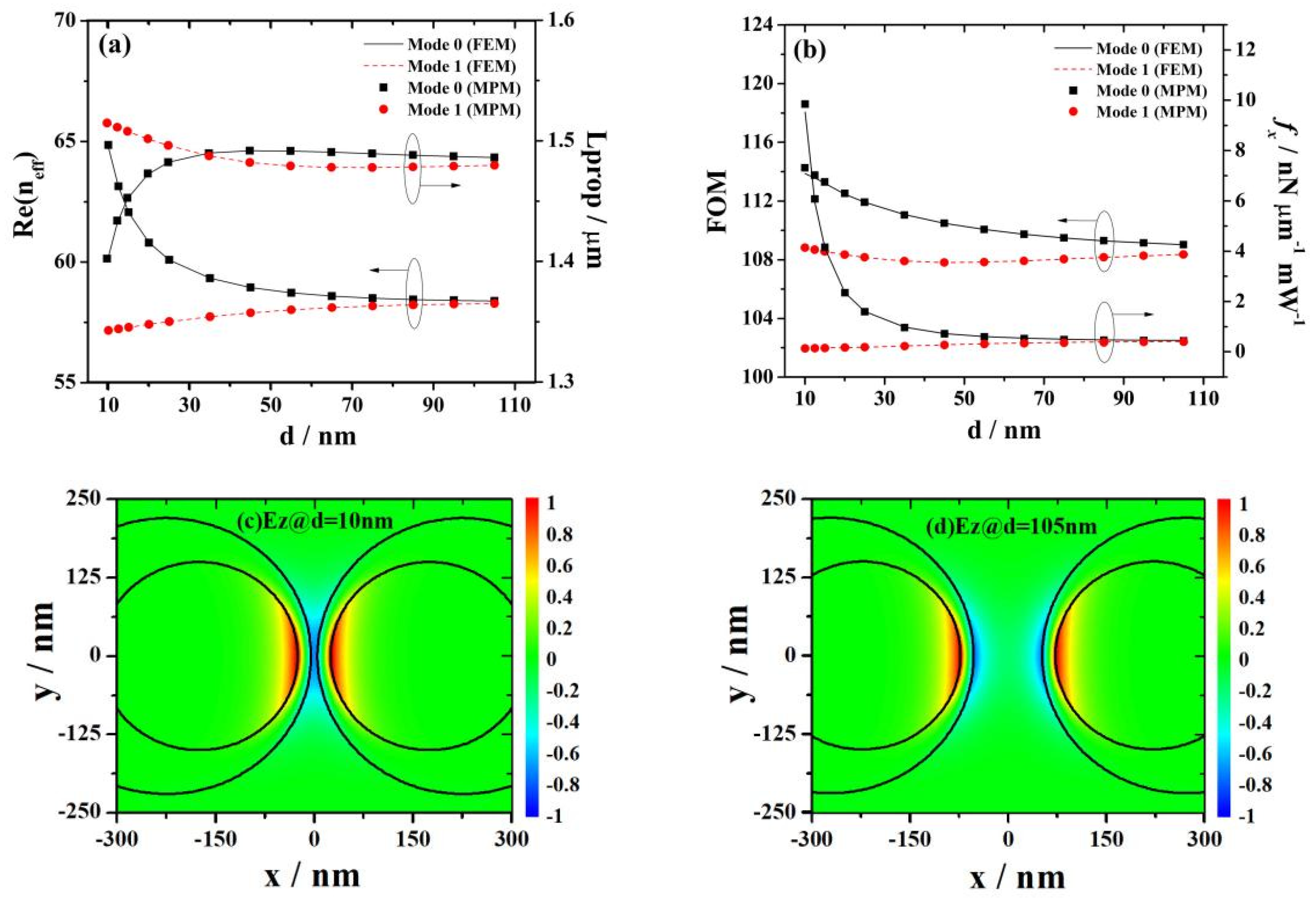
The relationship between the real part of the effective refractive index, propagation length, figure of merit, and normalized gradient force of the two modes with a minimum distance between the outer surfaces of the two parallel nanowires under the conditions of λ = 10 μ m , E f = 0.5 eV, ρ 10 = ρ 30 = 150 nm, ρ 20 = ρ 40 = 220 nm, s = 20 nm, n 1 = n 3 = 1.45, and n2 = n4 = 1.45 is shown in Figure 6a,b. It can be seen that within the range of 10–105 nm, as d increases, the R e ( n e f f ) and f x of mode 0 show a monotonic decreasing trend, while the R e ( n e f f ) and f x of mode 1 show a monotonic increasing trend. The L p r o p of mode 0 shows a monotonic upward trend, while the L p r o p of mode 1 shows a monotonic downward trend. The F O M of mode 0 shows a monotonic decreasing trend, while the F O M of mode 1 shows first a decreasing and then an increasing trend. Under certain wavelength conditions, mode 0 has a higher figure of merit and mode 1 has a lower figure of merit. The above phenomenon can be explained by the fact that the radii of different parent cylindrical nanowires correspond to different mode field distributions. Figure 6c,d respectively show the E z field distribution of mode 0 at d = 10 nm and 105 nm. Comparing the two graphs, it becomes apparent that as d decreases, field intensity is heightened and more focused on the graphene layer adjacent to the nanowires’ surfaces. This stronger interaction between the field and graphene leads to increased losses, shorter propagation distances, and a stronger normalized gradient force. Conversely, when d is larger, the field intensity diminishes and slightly penetrates into the gap between the nanowires. As a result, the interaction with the graphene weakens, resulting in reduced losses, longer propagation distances, and a weaker normalized gradient force.

3.7. Influence of the Minimum Distance between the Surface of the Embedded Cylinder and the Surface of the Parent Cylinder on Mode Characteristics

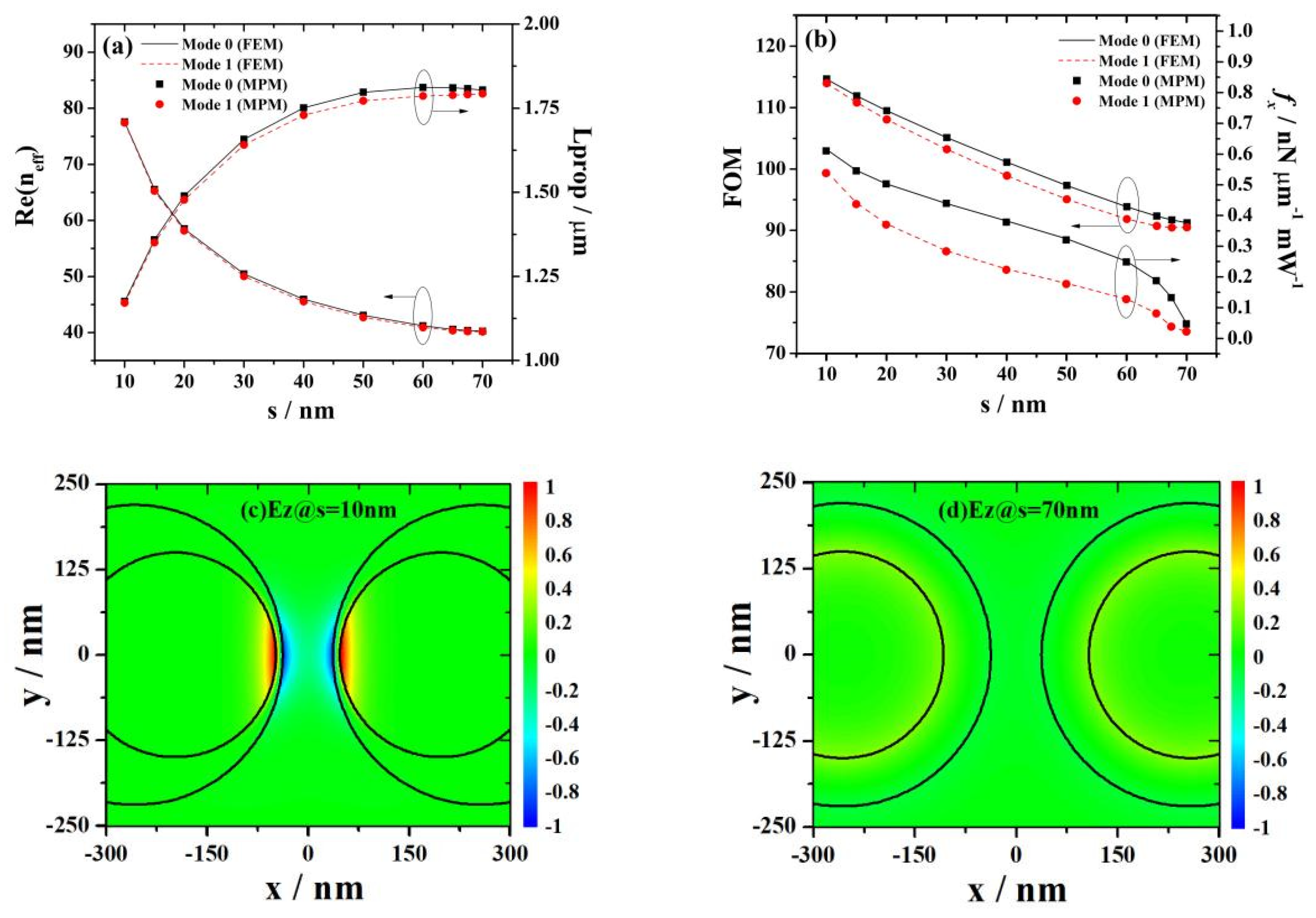
The relationship between the real part of the effective refractive index, propagation length, figure of merit, and normalized gradient force of the two modes with minimum spacing between the surface of the embedded cylindrical nanowire and the surface of the parent cylindrical nanowire under the conditions of λ = 10 μ m , E f = 0.5 eV, ρ 10 = ρ 30 = 150 nm, ρ 20 = ρ 40 = 220 nm, d = 75 nm, n 1 = n 3 = 1.45, and n 2 = n 4 = 1.45 is shown in Figure 7a,b. It can be seen that within the range of 10–70 nm, as s increases, the R e ( n e f f ) , F O M , and f x of the two modes all show a monotonic decreasing trend. Mode 0 has a slower descent speed, while mode 1 has a faster descent speed. The L p r o p of the two modes shows a monotonic growth trend. Mode 0 has a faster growth rate, while mode 1 has a slower growth rate. The above phenomenon can be explained by the fact that the minimum spacing between the surfaces of different embedded cylindrical nanowires and the surfaces of the parent cylindrical nanowires corresponds to different mode field distributions. Figure 7c,d respectively show the E z field distribution of mode 1 at s = 10 nm and 70 nm. Comparing the two graphs, it is evident that when s is small, the field is predominantly confined to the graphene layer adjacent to the nanowires’ surfaces. This results in a stronger interaction between the field and graphene, leading to increased losses, shortened propagation distances, and a stronger normalized gradient force. However, when s is large, the field is primarily distributed in the background space separating the nanowires. Consequently, the interaction between the field and graphene is weaker, leading to reduced losses, longer propagation distances, and a weaker normalized gradient force.

3.8. Influence of the Refractive Index of Region I (or Region III) on Mode Characteristics

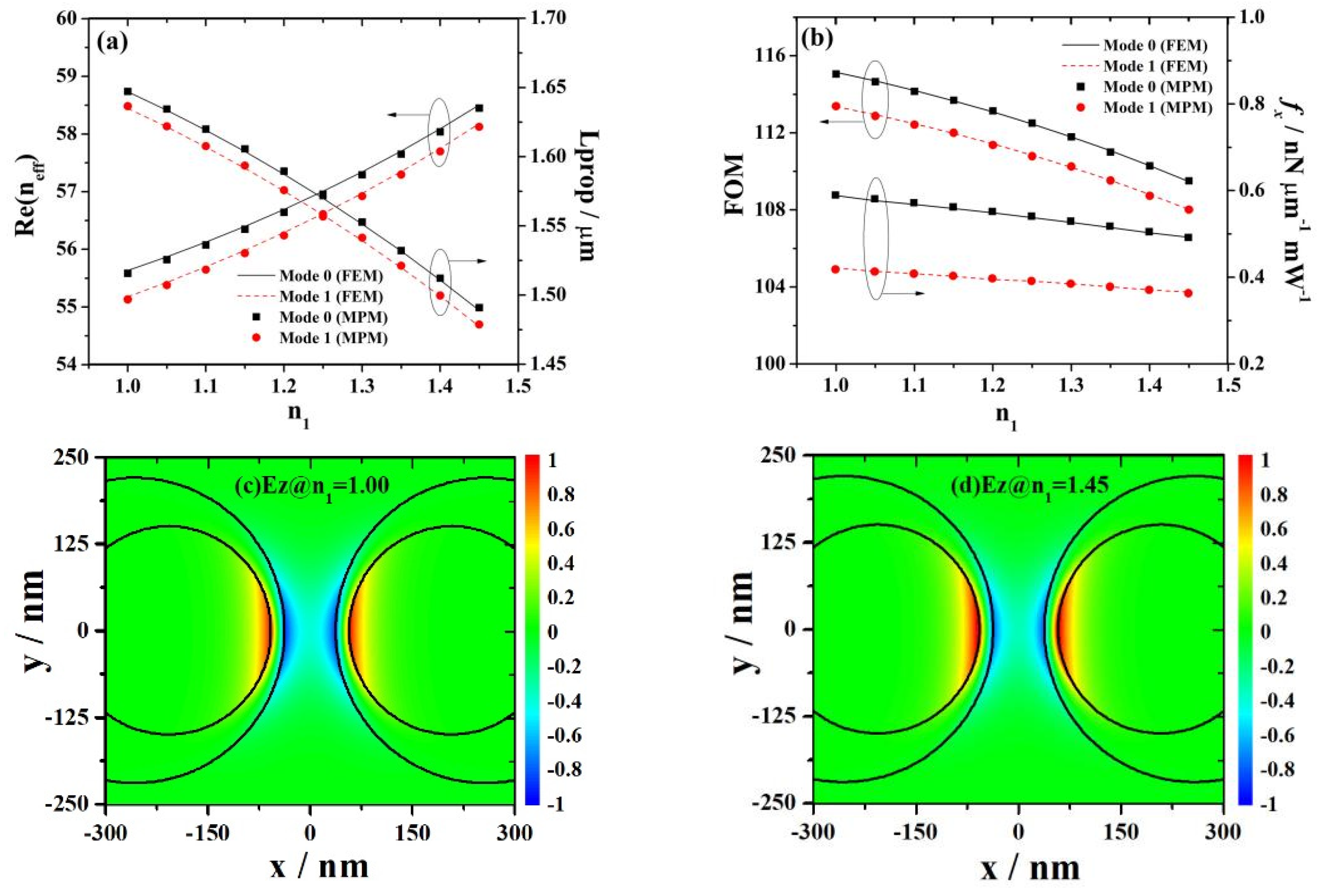
Under the conditions of λ = 10 μ m , E f = 0.5 eV, ρ 10 = ρ 30 = 150 nm, ρ 20 = ρ 40 = 220 nm, s = 20 nm, d = 75 nm, and n 2 = n 4 = 1.45, the relationship between the real part of the effective refractive index, propagation length, figure of merit, and normalized gradient force of the two modes and the refractive index n 1 (or n 3 ) of region I (or region III) is shown in Figure 8a,b. It can be seen that within the range of 1.00 (corresponding to the hollow case) to 1.45, as n 1 increases, the R e ( n e f f ) , F O M , and f x of the two modes all show a monotonic downward trend. Under certain refractive index conditions, R e ( n e f f ) , F O M , and f x of mode 0 are all higher than R e ( n e f f ) , F O M , and f x of mode 1. The L p r o p of both modes shows a monotonic growth trend. Under certain refractive index conditions, the L p r o p of mode 0 is higher than that of mode 1. The above phenomenon can be explained by the fact that different refractive indices in region I (or region III) correspond to different mode field distributions. Figure 8c,d, respectively, show the E z field distribution of mode 1 at n 1 = 1.00 and 1.45. Comparing the two graphs, it becomes apparent that when n 1 is small, the field tends to disperse within the space between the two nanowires. This results in a relatively weak interaction between the field and the graphene, leading to reduced losses, extended propagation distances, and weaker normalized gradient forces. Conversely, when n 1 is large, the field is primarily constrained to the graphene layer close to the nanowires’ surfaces. This stronger interaction between the field and graphene causes increased losses, shorter propagation distances, and stronger normalized gradient forces.
In Figure 2a, it can be seen that the propagation distance of mode 0 and mode 1 is almost the same. The reason for this phenomenon is that, when the working wavelength is changed, the intensity and distribution range of the field distribution corresponding to mode 1 and mode 0 are almost the same. The interaction between graphene and the field is also almost the same, and the pace of change is also almost the same. Therefore, the variation of propagation distance with wavelength is also almost the same. The same conclusion applies to changing the Fermi energy of graphene, as shown in Figure 3a. In Figure 4a, it can be seen that the propagation distance of mode 0 and mode 1 is slightly different. The reason for this phenomenon is that, when the radius of the embedded nanowire is changed, the intensity and distribution range of the field distribution corresponding to mode 1 and mode 0 are slightly different, the interaction between graphene and the field is also slightly different, and the pace of change is also slightly different. Therefore, the variation of propagation distance with the radius of the embedded nanowire is also slightly different. The same conclusion applies to changing other geometric structural parameters, as shown in Figure 5a, Figure 6a, and Figure 7a.
The nested dielectric parallel nanowire pairs coated with graphene display a significant gradient force that surpasses 100 nN·μm−1·mW−1, as clearly demonstrated in Figure 5b, Figure 6b, Figure 7b, and Figure 8b. This result surpasses the findings reported in reference [30].
The multipole method is a semi-analytical method, while the finite element method is a numerical method. In terms of the physical mechanism of pattern formation, the multipole method is superior to the finite element method.

4. Conclusions

In this paper, a kind of waveguide consisting of four nested cylindrical dielectric parallel nanowires coated with graphene was designed, and characteristics of the lowest two modes supported by this waveguide were analyzed using the multipole method. In this method, the longitudinal components of the field are expanded firstly by the Bessel function in four cylindrical coordinate systems; then, the characteristic equation of the mode is obtained by virtue of the superposition principle of the field and the boundary value relationship, and the effective refractive index of the mode and the corresponding mode field distribution are finally obtained by means of the linear algebra method. The obtained results of the multipole method have been confirmed by the finite element method. Assuming ρ 10 = ρ 30 , ρ 20 = ρ 40 , n 1 = n 3 , and n 2 = n 4 , we found that the R e ( n e f f ) , L p r o p , F O M , and f x of the two lowest modes can be adjusted by adjusting λ , E f , ρ 10 , ρ 20 , d , s , and n 1 . Utilizing a double-layer graphene structure, this waveguide demonstrates remarkable gradient forces, exceeding the performance of the comparable single-layer graphene structure. The various phenomena observed can be explained by the fact that different parameters correspond to different field distributions and different interactions between the field and graphene. The results of this article have certain theoretical guidance significance for the design, fabrication, and application of surface plasmon waveguides composed of nested parallel dielectric nanowire pairs with graphene coating.

Author Contributions

Investigation, writing—original draft preparation, L.Y.; validation, writing—review and editing, J.L.; methodology, software, supervision, W.X. All authors have read and agreed to the published version of the manuscript.

Funding

This research was funded by the Shanxi Scholarship Council of China, grant number 2023-141; the Fundamental Research Program of Shanxi Province, grant number 202103021224188, 202203021221101; and the Open Project of Key Laboratory, North University of China, grant number DXMBJJ2022-02.

Institutional Review Board Statement

Not applicable.

Informed Consent Statement

Not applicable.

Data Availability Statement

The data presented in this study are available on request from the corresponding author.

Acknowledgments

The authors thank Shanxi Cloud Era Technology Company Ltd. for its computing services for this work.

Conflicts of Interest

The authors declare no conflict of interest.

References

  1. Khan, Q.; Khan, A.; Bacha, B.A.; Khan, M.; Khesro, A. Sensitivity of the surface plasmon polariton waves at the interface of metal and dielectric medium using doppler broadening effect. Plasmonics 2024, 19, 123–129. [Google Scholar] [CrossRef]
  2. Xu, J.; Zhang, C.; Wang, Y.; Wang, M.; Xu, Y.; Wei, T.; Xie, Z.; Liu, S.; Lee, C.-K.; Hu, X.; et al. All-in-one, all-optical logic gates using liquid metal plasmon nonlinearity. Nat. Commun. 2024, 15, 1726. [Google Scholar] [CrossRef] [PubMed]
  3. Zulfajri, M.; Gedda, G.; Ulla, H.; Habibati; Gollavelli, G.; Huang, G.G. A review on the chemical and biological sensing applications of silver/carbon dots nanocomposites with their interaction mechanisms. Adv. Colloid Interface Sci. 2024, 325, 103115. [Google Scholar] [CrossRef]
  4. Vaidyanathan, A.; Mondal, B.; Rout, C.S.; Chakraborty, B. Plasmonic gas sensors based on nanomaterials: Mechanisms and recent developments. J. Phys. D Appl. Phys. 2024, 57, 263002. [Google Scholar] [CrossRef]
  5. Ramírez, M.O.; Molina, P.; Hernández-Pinilla, D.; López-Polín, G.; Ares, P.; Lozano-Martín, L.; Yan, H.; Wang, Y.; Sarkar, S.; Al Shuhaib, J.H.; et al. Integrating 2D materials and plasmonics on Lithium Niobate platforms for pulsed laser operation at the nanoscale. Laser Photonics Rev. 2024, 18, 2300817. [Google Scholar] [CrossRef]
  6. Fang, Y.; Sun, M. Nanoplasmonic waveguides: Towards applications in integrated nanophotonic circuits. Light Sci. Appl. 2015, 4, e294. [Google Scholar] [CrossRef]
  7. Boltasseva, A.; Nikolajsen, T.; Leosson, K.; Kjaer, K.; Larsen, M.; Bozhevolnyi, S. Integrated optical components utilizing long-range surface plasmon polaritons. J. Light. Technol. 2005, 23, 413–422. [Google Scholar] [CrossRef]
  8. Oulton, R.F.; Sorger, V.J.; Genov, D.A.; Pile, D.F.P.; Zhang, X. A hybrid plasmonic waveguide for subwavelength confinement and long-range propagation. Nat. Photonics 2008, 2, 496–500. [Google Scholar] [CrossRef]
  9. Kuppadakkath, A.; Najafidehaghani, E.; Gan, Z.; Tuniz, A.; Ngo, G.Q.; Knopf, H.; Löchner, F.J.F.; Abtahi, F.; Bucher, T.; Shradha, S.; et al. Direct growth of monolayer MoS2 on nanostructured silicon waveguides. Nanophotonics 2022, 11, 4397–4408. [Google Scholar] [CrossRef]
  10. Liu, Z.; Yang, C.; Wan, P.; Ding, L.; Xu, W. Dielectric-loaded black phosphorus surface plasmon polariton waveguides. Opt. Express 2019, 27, 18005–18015. [Google Scholar] [CrossRef]
  11. Berini, P. Plasmon–polariton modes guided by a metal film of finite width. Opt. Lett. 1999, 24, 1011–1013. [Google Scholar] [CrossRef]
  12. Nikitin, A.Y.; Guinea, F.; Garcia-Vidal, F.J.; Martín-Moreno, L. Edge and waveguide terahertz surface plasmon modes in graphene microribbons. Phys. Rev. B 2011, 84, 161407. [Google Scholar] [CrossRef]
  13. Liu, L.; Han, Z.; He, S. Novel surface plasmon waveguide for high integration. Opt. Express 2005, 13, 6645–6650. [Google Scholar] [CrossRef]
  14. He, S.; Zhang, X.; He, Y. Graphene nano-ribbon waveguides of recordsmall mode area and ultra-high effective refractive indices for future VLSI. Opt. Express 2013, 21, 30664–30673. [Google Scholar] [CrossRef] [PubMed]
  15. Pile, D.F.P.; Ogawa, T.; Gramotnev, D.K.; Okamoto, T.; Haraguchi, M.; Fukui, M.; Matsuo, S. Theoretical and experimental investigation of strongly localized plasmons on triangular metal wedges for subwavelength waveguiding. Appl. Phys. Lett. 2005, 87, 061106. [Google Scholar] [CrossRef]
  16. Liu, P.; Zhang, X.; Ma, Z.; Cai, W.; Wang, L.; Xu, J. Surface plasmon modes in graphene wedge and groove waveguides. Opt. Express 2013, 21, 32432–32440. [Google Scholar] [CrossRef] [PubMed]
  17. Gramotnev, D.K.; Pile, D.F.P. Single-mode subwavelength waveguide with channel plasmon-polaritons in triangular grooves on a metal surface. Appl. Phys. Lett. 2004, 85, 6323–6325. [Google Scholar] [CrossRef]
  18. Dai, D.; He, S. A silicon-based hybrid plasmonic waveguide with a metal cap for a nano-scale light confinement. Opt. Express 2009, 17, 16646–16653. [Google Scholar] [CrossRef]
  19. Saeed, M.; Ghaffar, A.; Rehman, S.; Naz, M.Y.; Shukrullah, S.; Naqvi, Q.A. Graphene-based plasmonic waveguides: A mini review. Plasmonics 2022, 17, 901–911. [Google Scholar] [CrossRef]
  20. Gao, Y.; Ren, G.; Zhu, B.; Wang, J.; Jian, S. Single-mode graphene-coated nanowire plasmonic waveguide. Opt. Lett. 2014, 39, 5909–5912. [Google Scholar] [CrossRef]
  21. Gao, Y.; Ren, G.; Zhu, B.; Liu, H.; Lian, Y.; Jian, S. Analytical model for plasmon modes in graphene-coated nanowire. Opt. Express 2014, 22, 24322–24331. [Google Scholar] [CrossRef]
  22. Liu, J.P.; Zhai, X.; Wang, L.L.; Li, H.-J.; Xie, F.; Lin, Q.; Xia, S.-X. Analysis of mid-infrared surface plasmon modes in a graphene-based cylindrical hybrid waveguide. Plasmonics 2016, 11, 703. [Google Scholar] [CrossRef]
  23. Yang, J.F.; Yang, J.J.; Deng, W.; Mao, F.; Huang, M. Transmission properties and molecular sensing application of CGPW. Opt. Express 2015, 23, 32289–32299. [Google Scholar] [CrossRef]
  24. Zhao, T.; Hu, M.; Zhong, R.; Chen, X.; Zhang, P.; Gong, S.; Zhang, C.; Liu, S. Plasmon modes of circular cylindrical doublelayer graphene. Opt. Express 2016, 24, 20461–20471. [Google Scholar] [CrossRef]
  25. Liu, J.P.; Zhai, X.; Xie, F.; Wang, L.-L.; Xia, S.-X.; Li, H.-J.; Luo, X.; Shang, X.-J. Analytical model of mid-infrared surface plasmon modes in a cylindrical long-range waveguide with double-layer graphene. J. Light. Technol. 2017, 35, 1971–1979. [Google Scholar] [CrossRef]
  26. Xing, R.; Jian, S. Numerical analysis on tunable multilayer nanoring waveguide. IEEE Photonics Technol. Lett. 2017, 29, 967–970. [Google Scholar] [CrossRef]
  27. Hajati, M.; Hajati, Y. High-performance and low-loss plasmon waveguiding in graphene-coated nanowire with substrate. J. Opt. Soc. Am. B 2016, 33, 2560. [Google Scholar] [CrossRef]
  28. Teng, D.; Wang, K.; Huan, Q.; Chen, W.; Li, Z. High-performance light transmission based on graphene plasmonic waveguides. J. Mater. Chem. C 2020, 8, 6832–6838. [Google Scholar] [CrossRef]
  29. Teng, D.; Yang, Y.; Guo, J.; Ma, W.; Tang, Y.; Wang, K. Efficient guiding mid-infrared waves with graphene-coated nanowire based plasmon waveguides. Results Phys. 2020, 17, 103169. [Google Scholar] [CrossRef]
  30. Zhu, B.; Ren, G.; Yang, Y.; Gao, Y.; Wu, B.; Lian, Y.; Wang, J.; Jian, S. Field enhancement and gradient force in the graphene-coated nanowire pairs. Plasmonics 2015, 10, 839–845. [Google Scholar] [CrossRef]
  31. Xing, R.; Jian, S. Numerical analysis on the multilayer nanoring waveguide pair. IEEE Photonics Technol. Lett. 2016, 28, 2779–2782. [Google Scholar] [CrossRef]
  32. Ye, S.; Wang, Z.; Sun, C.; Dong, C.; Wei, B.; Wu, B.; Jian, S. Plasmon-phonon-polariton modes and field enhancement in the graphene-coated hexagon boron nitride nanowire pairs. Opt. Express 2018, 26, 23854–23867. [Google Scholar] [CrossRef] [PubMed]
  33. Hajati, M.; Hajati, Y. Plasmonic characteristics of two vertically coupled graphene-coated nanowires integrated with substrate. Appl. Opt. 2017, 56, 870–875. [Google Scholar] [CrossRef]
  34. Teng, D.; Wang, K.; Huan, Q.; Zhao, Y.; Tang, Y. High-performance transmission of surface plasmons in graphene-covered nanowire pairs with substrate. Nanomaterials 2019, 9, 1594. [Google Scholar] [CrossRef] [PubMed]
  35. Kotsifaki, D.G.; Chormaic, S.N. Plasmonic optical tweezers based on nanostructures: Fundamentals, advances and prospects. Nanophotonics 2019, 8, 1227–1245. [Google Scholar] [CrossRef]
  36. Tan, H.; Hu, H.; Huang, L.; Qian, K. Plasmonic tweezers for optical manipulation and biomedical applications. Analyst 2020, 145, 5699–5712. [Google Scholar] [CrossRef]
  37. Hu, S.; Liao, Z.W.; Cai, L.; Jiang, X.X. Near-field optical tweezers for chemistry and biology. Phys. Status Solidi A 2020, 217, 1900604. [Google Scholar] [CrossRef]
  38. Li, H.; Cao, Y.; Zhou, L.; Xu, X.; Zhu, T.; Shi, Y.; Qiu, C.-W.; Ding, W. Optical pulling forces and their applications. Adv. Opt. Photonics 2020, 12, 288–366. [Google Scholar] [CrossRef]
  39. Zhang, Y.; Min, C.; Dou, X.; Wang, X.; Urbach, H.P.; Somekh, M.G.; Yuan, X. Plasmonic tweezers: For nanoscale optical trapping and beyond. Light Sci. Appl. 2021, 10, 59. [Google Scholar] [CrossRef]
  40. Zhou, L.M.; Shi, Y.; Zhu, X.; Hu, G.; Cao, G.; Hu, J.; Qiu, C.-W. Recent progress on optical micro/nanomanipulations: Structured forces, structured particles, and synergetic applications. ACS Nano 2022, 16, 13264–13278. [Google Scholar] [CrossRef]
  41. Samadi, M.; Alibeigloo, P.; Aqhili, A.; Khosravi, M.A.; Saeidi, F.; Vasini, S.; Ghorbanzadeh, M.; Darbari, S.; Moravvej-Farshi, M.K. Plasmonic tweezers: Towards nanoscale manipulation. Opt. Lasers Eng. 2022, 154, 107001. [Google Scholar] [CrossRef]
  42. Li, H.; Xue, W.; Li, N.; Du, Y.; Li, C. Mode characteristics of a graphene-coated cylindrical dielectric waveguide with a nested eccentric hollow elliptical cylinder. J. Opt. Soc. Am. B 2022, 39, 2944–2956. [Google Scholar] [CrossRef]
  43. Liu, J.; Yu, L.X.; Xue, W.R. Mode characteristics of nested eccentric waveguides constructed by two cylindrical nanowires coated with graphene. Chin. Phys. B 2022, 31, 036803. [Google Scholar] [CrossRef]
  44. Teng, D.; Wang, K.; Li, Z. Graphene-coated nanowire waveguides and their applications. Nanomaterials 2020, 10, 229. [Google Scholar] [CrossRef]
  45. Rezzouk, Y.; Khattou, S.; Amrani, M.; Noual, A.; El Boudouti, E.H.; Talbi, A.; Djafari-Rouhani, B. Bound states in the continuum and induced resonances in a simple plasmonic waveguide with sensing application. Photonics 2023, 10, 1284. [Google Scholar] [CrossRef]
  46. Nikitin, A.Y.; Guinea, F.; Garcia-Vidal, F.J.; Martin-Moreno, L. Fields radiated by a nanoemitter in a graphene sheet. Phys. Rev. B 2011, 84, 195446. [Google Scholar] [CrossRef]
  47. Golub, G.; van Loan, C.F. Matrix Computations, 4th ed.; The Johns Hopkins University Press: Baltimore, MD, USA, 2013. [Google Scholar]
  48. Teng, D.; Wang, K.; Li, Z.; Zhao, Y. Graphene-coated nanowire dimers for deep subwavelength waveguiding in mid-infrared range. Opt. Express 2019, 27, 12458–12469. [Google Scholar] [CrossRef]
  49. He, X.Q.; Ning, T.G.; Pei, L.; Zheng, J.J.; Li, J.; Wen, X.D. Tunable hybridization of graphene plasmons and dielectric modes for highly confined light transmit at terahertz wavelength. Opt. Express 2019, 27, 5961–5972. [Google Scholar] [CrossRef]
  50. Hajati, M.; Hajati, Y. Deep subwavelength confinement of mid-infrared plasmon modes by coupling graphene-coated nanowire with a dielectric substrate. Plasmonics 2018, 13, 403–412. [Google Scholar] [CrossRef]
  51. Novotny, L.; Hecht, B. Principles of Nano-Optics, 2nd ed.; Cambridge University Press: Cambridge, UK, 2012. [Google Scholar]
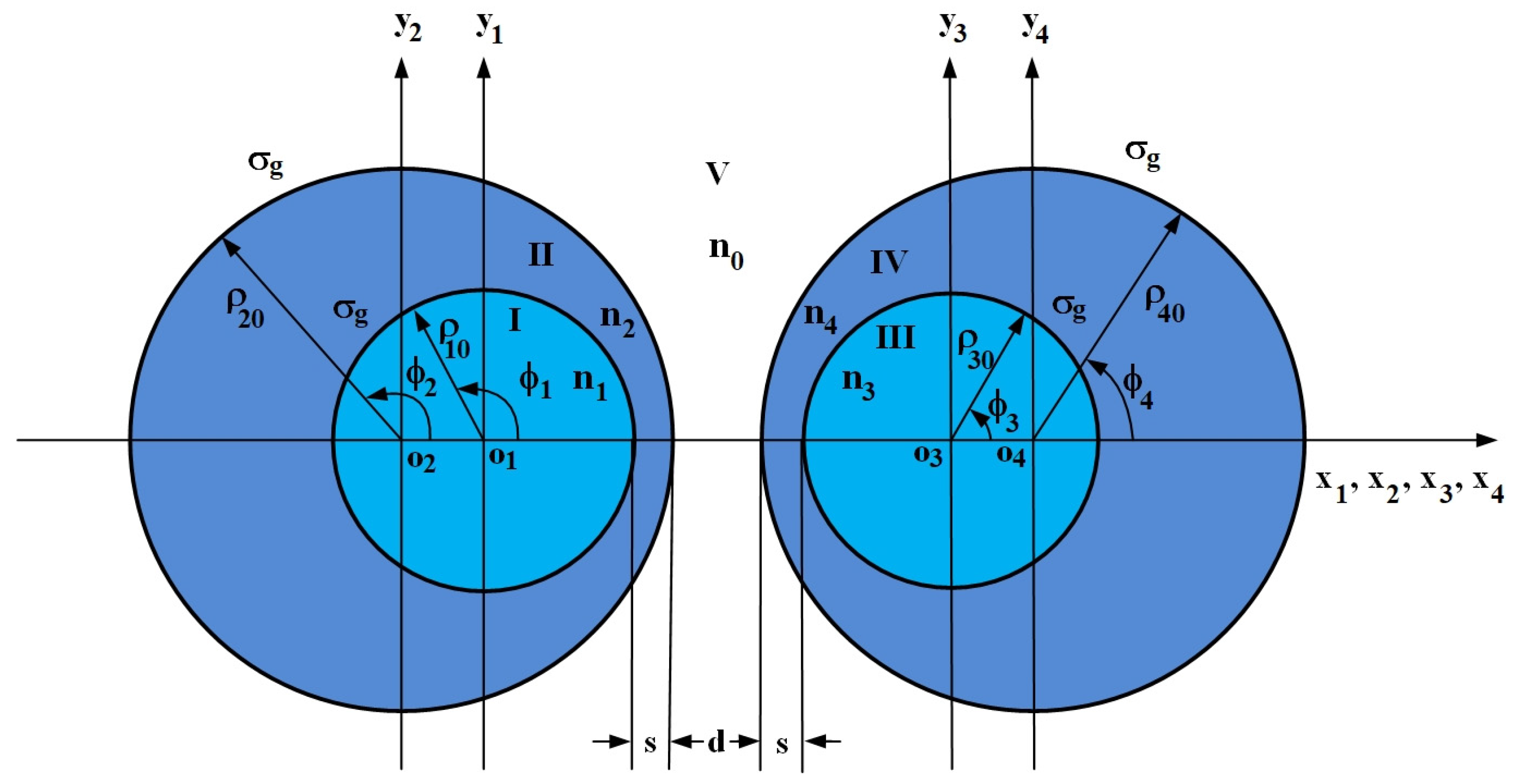
Figure 1. Cross-sectional view of a waveguide composed of two nested cylindrical dielectric parallel nanowires coated with graphene.
Photonics 11 00441 g001
Figure 2. The dependence of R e ( n e f f ) and L p r o p (a), F O M and f x (b) on the working wavelength. The E z field distribution of mode 1 at λ = 8 μ m (c) and 14 μ m (d).
Photonics 11 00441 g002
Figure 3. The dependence of R e ( n e f f ) and L p r o p (a), F O M and f x (b) on the Fermi energy of graphene. The E z field distribution of mode 1 at E f = 0.2 eV (c) and 1.2 eV (d).
Photonics 11 00441 g003
Figure 4. The dependence of R e ( n e f f ) and L p r o p (a), F O M and f x (b) on the radii of the 1st nanowire. The E z field distribution of mode 1 at ρ 10 = 80 nm (c) and 200 nm (d).
Photonics 11 00441 g004
Figure 5. The dependence of R e ( n e f f ) and L p r o p (a), F O M and f x (b) on the radii of the 2nd nanowire. The E z field distribution of mode 1 at ρ 20 = 170 nm (c) and 230 nm (d).
Photonics 11 00441 g005
Figure 6. The dependence of R e ( n e f f ) and L p r o p (a), F O M and f x (b) on the minimum distance between the outer surfaces of two parallel nanowires. The E z field distribution of mode 1 at d = 10 nm (c) and 105 nm (d).
Photonics 11 00441 g006
Figure 7. The dependence of R e ( n e f f ) and L p r o p (a), F O M and f x (b) on the minimum distance between the surface of the embedded cylinder and the surface of the parent cylinder. The E z field distribution of mode 1 at s = 10 nm (c) and 70 nm (d).
Photonics 11 00441 g007
Figure 8. The dependence of R e ( n e f f ) and L p r o p (a), F O M and f x (b) on the refractive index of region I (or region III). The E z field distribution of mode 1 at n 1 = 1.00 (c) and 1.45 nm (d).
Photonics 11 00441 g008
Table 1. Combination and the electric field component in the z direction of the two-lowest order modes.
ModeCombination E z
0Photonics 11 00441 i001Photonics 11 00441 i002
1Photonics 11 00441 i003Photonics 11 00441 i004
Disclaimer/Publisher’s Note: The statements, opinions and data contained in all publications are solely those of the individual author(s) and contributor(s) and not of MDPI and/or the editor(s). MDPI and/or the editor(s) disclaim responsibility for any injury to people or property resulting from any ideas, methods, instructions or products referred to in the content.