Article

Plasmon Response in Individual Conical Silicon Nanowires with Different Lengths

by
Rizwan Rafique
1,2,
Antonino La Magna
1,
Antonio Massimiliano Mio
1,
Salvatore Patanè
2,
Jost Adam
3,4 and
Rosaria Anna Puglisi
1,*
1
CNR—Istituto per la Microelettronica e Microsistemi, Strada Ottava 5, Zona Industriale, 95121 Catania, Italy
2
Department of Mathematics and Computer Science, Physics and Earth Science (MIFT), University of Messina, Viale F. Stagno d’Alcontres 31, 98166 Messina, Italy
3
Computational Materials and Photonics, EECS, University of Kassel, Wilhelmshöher Allee 71, D-34121 Kassel, Germany
4
Center for Interdisciplinary Nanostructure Science and Technology (CINSaT), University of Kassel, Heinrich-Plett-Str. 40, D-34132 Kassel, Germany
*
Author to whom correspondence should be addressed.
Photonics 2024, 11(11), 999; https://doi.org/10.3390/photonics11110999
Submission received: 15 September 2024 / Revised: 15 October 2024 / Accepted: 16 October 2024 / Published: 23 October 2024
(This article belongs to the Special Issue New Insights in Low-Dimensional Optoelectronic Materials and Devices)

Abstract

:
Silicon nanowires (SiNWs) are extensively studied in the scientific community due to their remarkable electrical and optical properties. In our previous studies, we have demonstrated that cylindrical−shaped SiNWs sustain longitudinal plasmon resonances (LPRs) and transverse plasmon resonances (TPRs). In this work, we will present the results of our investigation on conical SiNWs with different lengths and demonstrate that the NW size plays a role on the spectral response. We selected two groups of SiNWs with approximately 300 nm and 750 nm in length with different lengths and diameters. We investigated the optical properties of the SiNWs at a high energy and spatial resolution by using transmission electron microscopy and in situ electron energy loss spectroscopy. In the UV region of the spectrum investigated here, the experimental evidence suggests the presence of LPRs and a clear presence of TPRs. We found that, as the NW length increases, the LPR fundamental mode shifts towards higher energies, while the diameter seems to affect the TPR, shifting it to lower energy levels when the diameter increases. These SiNWs can play a role in the development of low−dimensional devices for applications in nano−electronics and nano−photonics.

1. Introduction

NWs are extensively studied in the scientific community due to their remarkable electrical and optical properties [1,2]. Recent research efforts have particularly focused on SiNWs due to silicon’s abundance, stability, and non−toxic nature [2,3,4,5]. Owing to their low cost, stability, and high efficiency, SiNWs are considered highly promising candidates for the development of next−generation low−dimensional devices, including applications in nano−electronics, nano−photonics, and advanced plasmonic systems [2,6,7,8,9,10,11]. Additionally, SiNWs have attracted significant attention in the field of photovoltaics due to their potential to enhance the efficiency and cost−effectiveness of solar cells [12,13,14]. These nanowires decouple photon absorption from the carrier collection path, thereby increasing the exciton generation rate through enhanced light trapping. Furthermore, SiNWs contribute to improved radiation coupling and reduced thermalization losses, owing to quantum confinement effects that lead to bandgap modulation [2,5,15,16,17,18]. This enables an efficient conversion of high−energy photons, particularly in the blue spectral region, into electrical energy, thus improving the overall performance of solar cells [2]. Plasmon resonance (PR) in metallic−dielectric systems is a key phenomenon characterized by the coupling of incident electromagnetic radiation with the collective oscillations of conduction electrons at the interface [19,20]. Resonance occurs when the frequency of the incident radiation matches the natural oscillation frequency of the electrons, resulting in a localized enhancement of the electromagnetic field. PR is of particular interest in photonics and optoelectronics because it enables the concentration of electromagnetic radiation into sub−wavelength volumes, thereby enhancing the local electric field. PR has been recently demonstrated in SiNWs [19,20]. Two types of plasmonic resonances have been observed in these nanostructures: LPR and TPR [19]. LPR occurs along the nanowire’s long axis, with resonance signals appearing at various locations depending on the nanowire’s geometry and morphology. In contrast, TPR manifests along the sidewalls of nanowires. To study these plasmonic modes, electron energy loss spectroscopy (EELS) conducted within a scanning transmission electron microscope (STEM), is indicated as one of the most useful techniques to investigate these phenomena at a high spatial and energy resolution [21]. STEM enables atomic−scale imaging, which allows for precise visualization of the structural features of SiNWs. This is crucial for correlating the NWs’ geometry with their plasmonic properties. On the other hand, EELS provides information about the elemental composition and electronic structure of materials. EELS, conducted within a STEM, has demonstrated significant efficacy in the characterization of surface plasmons [21]. By combining STEM and EELS, it is possible to obtain EELS maps with a spatial resolution sufficient to map the plasmonic distribution along the nanowire. Together, these techniques provide a powerful approach for analyzing the structural and electronic properties of SiNWs, offering a more holistic insight into plasmonic behavior. In our previous studies, we have demonstrated that cylindrical−shaped SiNWs sustain both LPRs and TPRs, and these resonances appear in the UV region of the spectrum [19,20]. In our recent work, we observed tapered−morphology SiNWs, and the results suggested the presence of TPR along with a continuous signal extending along the length of the SiNWs [22]. In this work, we will present the results of our investigation on conical SiNWs and demonstrate that these nanostructures exhibit different spectral behaviors compared to cylindrical nanowires. The synthesis of SiNWs has been obtained by vapor liquid−solid growth [3,4,5,23,24,25,26,27,28,29,30,31,32,33,34]. We selected two groups of SiNWs with approximately 300 nm and 750 nm in length, and with 15 nm and 44 nm in diameter, measured at the NW base. We investigated the optical properties of the SiNWs at a high energy and spatial resolution by using transmission electron microscopy and in situ EELS. In the UV region of the spectrum investigated here, the experimental evidence suggests the presence of plasmonic resonances and clear presence of TPR as in the previous cases, with peculiarities related to the new geometries reported in the following.

2. Methods

STEM and EELS were performed by using a JEOL ARM200F (JEOL Ltd., Tokyo, Japan) Cs−corrected microscope, equipped with a cold−field emission gun and operating at 200 keV. A GIF Quantum ER system (Gatan AMETEK, Pleasanton, CA, USA) was used for EELS measurements. EELS spectra were acquired in spectrum imaging (SI) mode. SI acquisition mode provided a 3D datacube containing annular dark field signal and low−loss EELS spectrum point by point, simultaneously. Spectra have been analyzed using Gatan DigitalMicrograph software, Version 3.6 (Gatan AMETEK, Pleasanton, CA, USA). The STEM analysis allows us to observe the sample at the atomic scale with a spatial resolution of 0.7 Angstrom (Å). In the present case, when we observe the entire NWs, the actual spatial resolution is about 1 nm, limited for the pixel size for an acquisition with a field of view of about 1 µm. Regarding the sample preparation, we collected NWs manually from the sample to the grid, with this not modifying the physical or chemical properties of NWs. During the TEM analysis, if SiNWs are in a tilted position with respect to the electron beam, we first align them to be perpendicular to the electron beam probe. After the alignment, the error on the control on tilt angle is around 5°, which corresponds to a relative error of 1% in terms of the spatial resolution. Before starting the measurement, we measure the zero−loss peaks (ZLPs) from the electron gun without exposing the sample. The ZLPs correspond to the energy of incident electrons that have not lost any energy, serving as a reference point in the spectrum and a measure of energy resolution, allowing us to isolate peaks corresponding to plasmon energy losses from background signals. The intensity and shape of the ZLPs provide quantitative information about the energy resolution. In our case, the FWHM of ZLPs is about 0.5 eV, with the latter being the resolution achievable with the technique used. In semiconductors, the energy width of the plasmon signals is larger, so these values do not have a significant impact on the detection of plasmon signals. For each experimental spectrum, a ZLP is acquired together with the plasmon responses, allowing a precise recalibration in case of a ZLP shift. In our experimental setup, the primary electron beam scan was carried out across a single NW. The EELS was acquired with an bin energy of 0.025 eV, while the energy resolution was about 0.5 eV. We removed the zero−loss contribution from the raw SI, extracting the corresponding zero−loss spectrum in the vacuum. For each energy value, E, EFSI was obtained by extracting the corresponding SI energy map in a range between E-0.25 eV and E+0.25 eV [20]. EFSI maps and EELS spectra were acquired for two different groups of conical SiNWs. The data were extracted along the long axis of SiNWs to observe the presence of LPR spots and then along the radial direction to observe the TPR spots. To properly investigate the existence of TPR spots, data were acquired by selecting a small rectangle starting from the base to the tip of SiNWs.

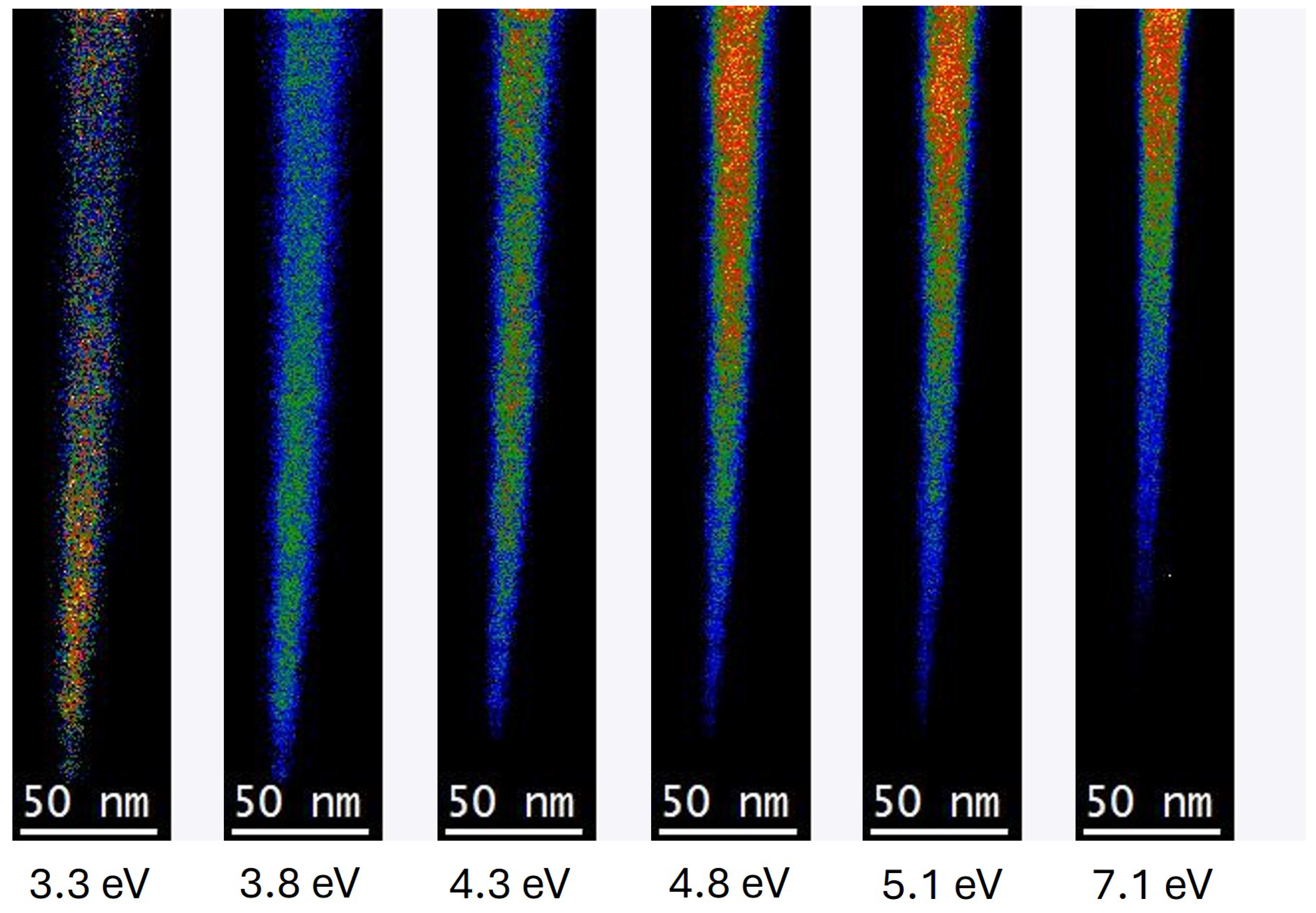
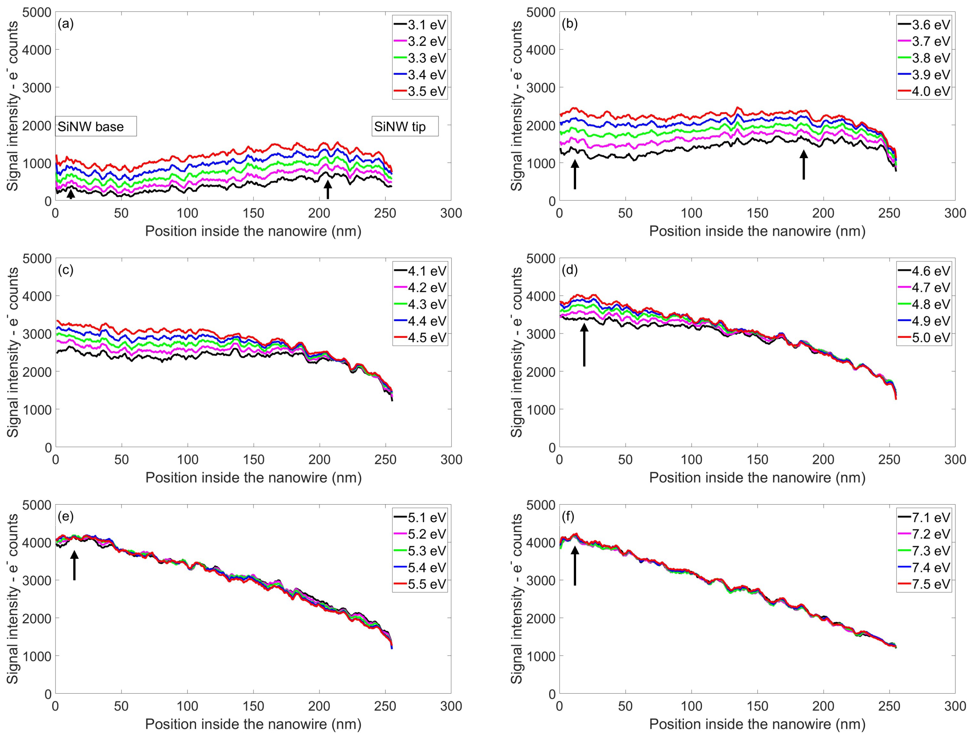
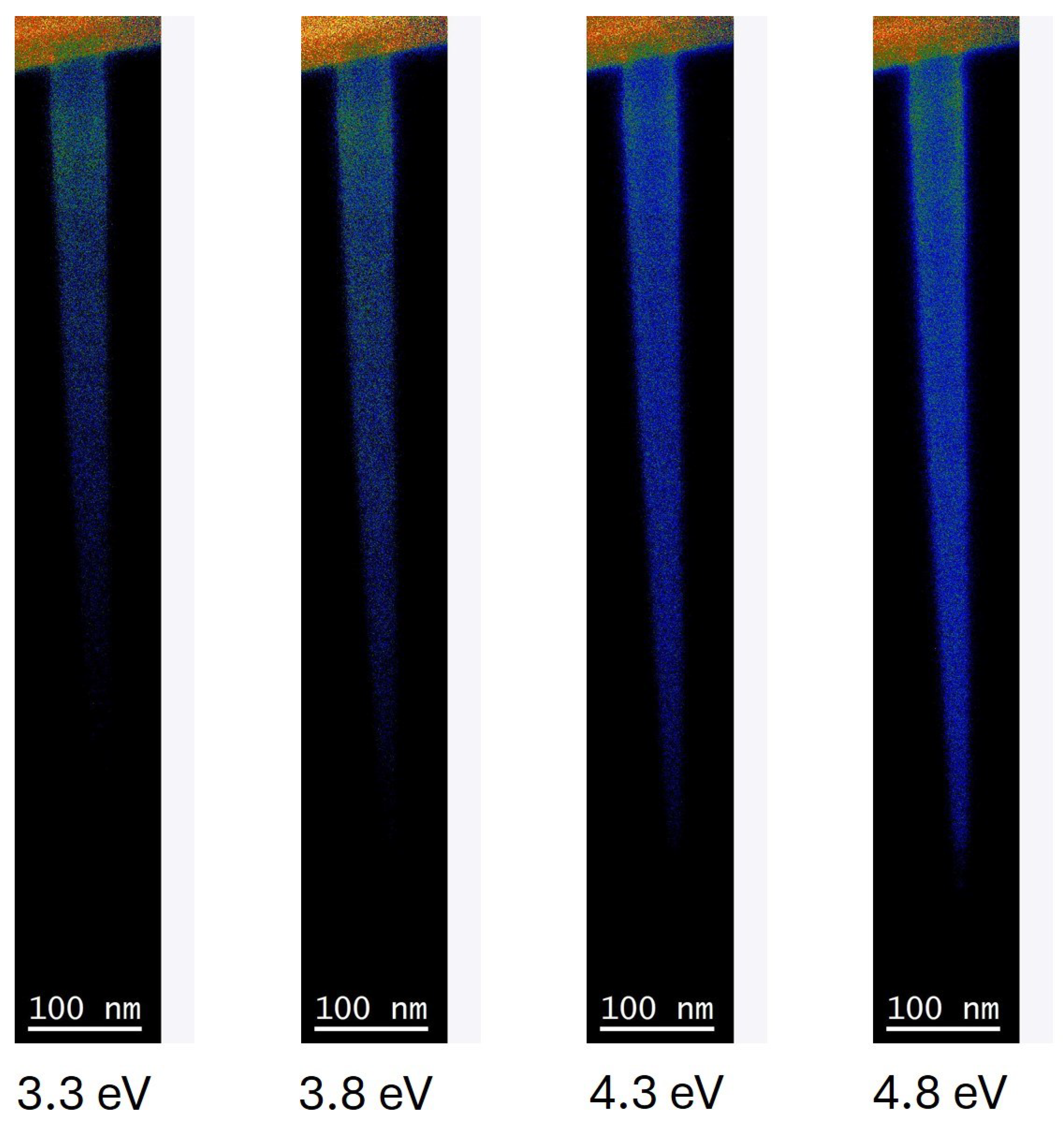
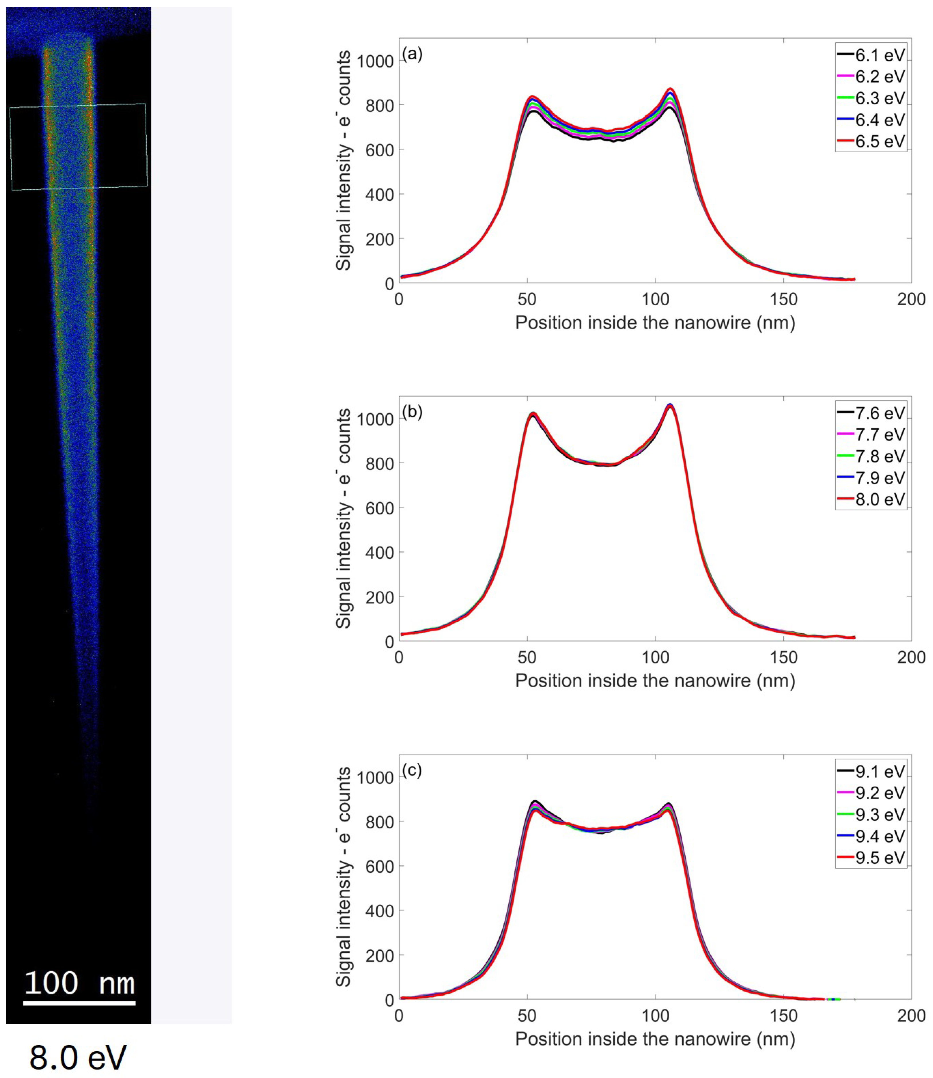
3. Results and Discussion

We selected SiNWs based on their dimensions and characterized them using EELS and STEM.
Figure 1 presents the energy−filtered spectroscopic images (EFSIs) of a conical silicon nanowire. The SiNW has a SiO2 shell with a thickness of 2.2 nm and a total length of 334 nm. The diameter of the nanowire is 15.1 nm at the base, 12.2 nm at the center, and tapers down to 5.7 nm at the tip. These nanowires, with their small tip diameter, fall within the quantum regime. Figure 1 displays EFSI maps at various energy values of 3.3 eV, 3.8 eV, 4.3 eV, 4.8 eV, 5.1 eV, and 7.1 eV, showing the most significant results, as explained below. No signal spot was observed at the tip of the nanowire at any of the investigated energies, indicating the absence of a tip effect in these nanostructures [19,20].
In Figure 2a, two peaks are observed at the base and near the tip of the SiNW, indicated by the arrows, suggesting the presence of an LPR mode. As the energy value increases from 3.1 eV to 3.5 eV, a corresponding increment in intensity is also observed. Figure 2b shows that further increases in energy lead to the gradual disappearance of the peaks, which vanish completely at 4.0 eV. Figure 2c confirms the absence of peaks between 4.1 eV and 4.5 eV, indicating no detectable signal in this range. Figure 2d demonstrates that, with increasing energy values, the intensity rises, and a new peak appears at the base of the SiNW. This peak becomes more pronounced as the energy increases. Figure 2e clearly shows a peak in the range: 5.1–5.5 eV, confirming the possible presence of LPR in the SiNW. However, this peak diminishes and disappears above 6 eV. Figure 2f further confirms the presence of an additional peak at 7.1 eV, which could be associated with LPR.
Figure 3 shows an EFSI image illustrating the shifting of signals along the walls of the SiNW (the rectangle inset represents the area of signal extraction). Figure 3a–c clearly suggest the presence of TPR in SiNW of length 334 nm. Figure 3a shows the presence of TPR at 8.1 eV, which becomes more pronounced with increasing energy. Figure 3b shows a clear presence of TPR in the range of 9.1–9.5 eV. In Figure 3c, the TPR signal begins to disappear beyond 10.1 eV. We observed high−intensity TPR signals at the base of the nanowires, which decreased as we moved toward the middle and completely disappeared in the middle of the SiNW (reported in the Supplementary Information (SI) of the manuscript (Figures S1–S6)).
In Figure 4, energy−filtered spectroscopic maps of another conical SiNW, from the group of the 750 nm long SiNWs, are presented. The SiNW has an oxide 2 shell with a thickness of 2.5 nm and a total length of 750 nm. The diameters of the SiNW are 44.4 nm at the base, 30 nm at the center, and 10.7 nm at the tip. EFSI maps were collected at energy values of 3.3 eV, 3.8 eV, 4.3 eV, and 4.8 eV, chosen among the most significant, as described below. Similar to the previous case, no signal spot was observed at the tip of the nanowire at any of the energy levels investigated, confirming the absence of the tip effect.
Figure 5a shows a peak that appears at the base of the SiNW, suggesting the presence of LPR. As the energy increases from 3.1 eV to 3.5 eV, the intensity also increases. Figure 5b,c demonstrate that as the energy increases further, the peak gradually disappears. Figure 5d reveals that increasing energy beyond this range leads to a rise in intensity, and two distinct peaks emerge between 4.6 and 5.0 eV, suggesting the presence of LPR in the SiNW.
Figure 6 shows the EFSI image, indicating the shifting of signals along the walls of the SiNW (the rectangle inset represents the area of signal extraction). Figure 6a confirms the appearance of TPR at 6.1 eV, which becomes more evident with increasing energy. Figure 6b shows a clear presence of TPR in the range of 7.6–8.0 eV, while Figure 6c demonstrates that the TPR signal begins to disappear beyond 9.1 eV as the energy continues to increase. With a similar observation to the 334 nm long SiNW high−intensity signals observed at the base of SiNW and as we move down, the intensity of TPR signals decreases and eventually disappears in the middle of the SiNW (reported in the Supplementary Information (SI) of the manuscript (Figures S7–S16).
These results suggest the possible presence of LPR in both SiNWs but at different positions and energy values, as well as a clear presence of TPR in both SiNWs groups. In the SiNWs from the group of 300 nm and with a base diameter of 15.1 nm, two distinct peaks were observed−one at the base and another near the tip of the nanowire, within the energy range of 3.1 eV to 4.0 eV−suggesting the presence of first harmonic modes in these nanostructures. No peaks were detected in the energy range from 4.1 to 4.5 eV. However, in the higher energy range of 4.6 to 5.0 eV, a single peak appeared at the base of the nanowire. Additionally, a peak at the base was detected in the energy range of 5.1 eV to 7.5 eV, suggesting the presence of another LPR mode. For energy values exceeding 8.1 eV, the signal spots exhibited a continuous pattern transitioning from the nanowire core to the walls of the nanostructures, indicating TPR. Within the energy range of 9.1 eV to 9.5 eV, strong TPR was observed. In the conical SiNWs from the group of 750 nm and with a base diameter of 44.4 nm, a single peak was detected at the base of the nanowire within the energy range of 3.1 eV to 4.5 eV. At higher energies, specifically between 4.6 eV and 5.0 eV, two peaks appeared at the base of the nanowire, suggesting the presence of the first harmonic resonance. For energy values above 6.0 eV, the signal spots became continuous, shifting from the nanowire core to its walls, also indicating the appearance of the transversal plasmonic response in this case. Within the energy range of 7.6 eV to 8.0 eV, strong TPR was observed. From the above results, the nanowire length effect on LPR is evident. SiNWs with shorter lengths exhibit harmonic behavior at lower energy ranges, while SiNWs with longer lengths demonstrate harmonic behavior at higher energy ranges. Additionally, an interesting role of diameter on TPR is observed. SiNWs with smaller diameters exhibit TPR at higher energy values, whereas those with larger diameters display TPR at lower energy values. If we compare these results to the previous ones, on cylindrical SiNWs, with a length of around 420 nm, the fundamental harmonic was observed at about 3.7 eV. In these cylindrical NWs, which presented a diameter of 30 nm, the TPR was observed at 8.5 eV [19] and these results are consistent with those observed here. In both groups, the results confirm the existence of TPR signals from the base to the middle of the SiNWs with respect to energies (reported in the SI of the manuscript). The peak−to−valley ratio (PVR), reported in the SI, calculated for the 750 nm group shows values generally larger than that for the 300 nm group. At low energy values (about 8 eV for the 300 nm, and about 6 eV for the 750 nm group), the PVR decreases as we move from the base to the tip of the nanowire. At higher energy values, we start to observe a shoulder in the PVR curves, appearing from the second explored position onwards. For the 300 nm group, this shoulder appears at 10 eV, where the PVR has a Gaussian−like trend. For the 750 nm case, this trend appears for all the energies from 9.1 eV to 9.5 eV. This trend might indicate the presence of a ‘tail’ of LPR’s contribution in its high−order modes inside the Si core of the nanostructure, still present at high energies, where we expect to observe only the TPR phenomenon. This is an interesting phenomenon that needs to be addressed in a hybrid mode, as already observed in ref. [35], and it should be further investigated. A final important observation is related to the fact that with regard to the tip, where the SiNW diameter enters the quantum regime, all TPR signals disappear, once again strongly evidencing the role of the diameter’s size on transversal oscillations.
These findings indicate that plasmonic behavior depends on the shape and geometry of SiNWs, also when the nanostructures have conical shapes. Variations in length and diameter seem to influence the position of plasmonic spots. The results clearly suggest the presence of TPR in both cases. For the 300 nm group of SiNWs, TPR was observed at 9.3 eV, and for the 750 nm group, TPR was observed at 8.0 eV. No tip effect was observed at any investigated values, indicating that tapering eliminates the tip effect that is seen in non−tapered NWs.

4. Conclusions

At the several investigated energy values, for the two groups of SiNWs that were approximately 300 nm and 750 nm in length, the experimental evidence suggests the presence of LPR and a clear presence of TPR, but at different positions and energy values. For the group of SiNWs with a length of 300 nm, we observed LPR at the tip and the base of the nanowire. In contrast, for the 750 nm group of SiNWs, we only observed LPR at the base. Variations in length and diameter seem to influence the position of plasmonic spots.

Supplementary Materials

The following supporting information can be downloaded at: https://www.mdpi.com/article/10.3390/photonics11110999/s1, Figure S1. EFSI map acquired at energy 9.3 eV (on the left). Signal intensity as a function of position, extracted along the radial axis of a 334 nm SiNW. The signal intensity was measured for different energy ranges to analyse TPR signals, at the position indicated by the white rectangle on the left. The energy intervals investigated are as follows: (a) 8.1 eV to 8.5 eV, (b) 8.6 eV to 9.0 eV, (c) 9.1 eV to 9.5 eV, (d) 9.6 eV to 10.0 eV, and (e) 10.1 eV to 10.5 eV. Figure S2. Signal intensity measured for different energy ranges, listed in Figure S1, at the position indicated by the white rectangle on the left. Figure S3. Signal intensity measured for different energy ranges, listed in Figure S1, at the position indicated by the white rectangle on the left. Figure S4. Signal intensity measured for different energy ranges, listed in Figure S1, at the position indicated by the white rectangle on the left. Figure S5. Signal intensity measured for different energy ranges, listed in Figure S1, at the position indicated by the white rectangle on the left. Figure S6. Signal intensity measured for different energy ranges, listed in Figure S1, at the position indicated by the white rectangle on the left. Figure S7. EFSI map acquired at energy 8.0 eV (on the left). Signal intensity as a function of position, extracted along the radial axis of a 750 nm SiNW. The signal intensity was measured for different energy ranges to analyse TPR signals, at the position indicated by the white rectangle on the left. The energy intervals investigated are as follows: (a) 6.1 eV to 6.5 eV, (b) 7.1 eV to 7.5 eV, (c) 7.6 eV to 8.0 eV, and (e) 9.1 eV to 9.5 eV. Figure S8. Signal intensity measured for different energy ranges, listed in Figure S7, at the position indicated by the white rectangle on the left. Figure S9. Signal intensity measured for different energy ranges, listed in Figure S7, at the position indicated by the white rectangle on the left. Figure S10. Signal intensity measured for different energy ranges, listed in Figure S7, at the position indicated by the white rectangle on the left. Figure S11. Signal intensity measured for different energy ranges, listed in Figure S7, at the position indicated by the white rectangle on the left. Figure S12. Signal intensity measured for different energy ranges, listed in Figure S7, at the position indicated by the white rectangle on the left. Figure S13. Signal intensity measured for different energy ranges, listed in Figure S7, at the position indicated by the white rectangle on the left. Figure S14. Signal intensity measured for different energy ranges, listed in Figure S7, at the position indicated by the white rectangle on the left. Figure S15. Signal intensity measured for different energy ranges, listed in Figure S7, at the position indicated by the white rectangle on the left. Figure S16. Signal intensity measured for different energy ranges, listed in Figure S7, at the position indicated by the white rectangle on the left. Figure S17. Peak-to-valley ratio as a function of position to investigate the TPR behavior of SiNWs. Figure S17a displays the TPR signals behaviour at six different positions (from base to tip) of SiNW from the 300 nm group. Figure S17b displays the TPR signals behaviour at five different positions (from base to tip) of SiNW from the 750 nm group.

Author Contributions

Conceptualization, R.A.P.; data curation, R.A.P., R.R. and A.M.M.; formal analysis, R.R. and A.M.M.; funding acquisition, R.A.P. and A.L.M.; investigation, R.A.P., R.R. and A.M.M.; project administration, A.L.M.; resources, A.L.M.; supervision, R.A.P., S.P. and J.A.; writing—original draft, R.R.; writing—review and editing, R.A.P., A.M.M. and J.A. All authors have read and agreed to the published version of the manuscript.

Funding

R.A.P., A.M.M. and A.L.M. acknowledge the following projects for funding: NextGenerationEU, M4C2, within the PNRR project NFFA—DI, CUP B53C22004310006, IR0000015, having benefited from the access provided by CNR−IMM@CT in Catania.

Data Availability Statement

No publicly archived datasets were created.

Conflicts of Interest

The authors declare no conflicts of interest.

Abbreviations

The following abbreviations are used in this manuscript:
NWsSemiconductor nanowires
SiNWsSilicon nanowires
LPRLongitudinal plasmon resonance
TPRTransverse plasmon resonance
PRPlasmon resonance
EELSElectron energy loss spectroscopy
STEMScanning transmission electron microscope
SISupplementary information
EFSIEnergy−filtered spectroscopic images

References

  1. Kayes, B.M.; Atwater, H.A.; Lewis, N.S. Comparison of the device physics principles of planar and radial p-n junction nanorod solar cells. J. Appl. Phys. 2005, 97, 114302. [Google Scholar] [CrossRef]
  2. Stelzner, T.; Pietsch, M.; Andrä, G.; Falk, F.; Ose, E.; Christiansen, S. Silicon nanowire-based solar cells. Nanotechnology 2008, 19, 295203. [Google Scholar] [CrossRef] [PubMed]
  3. Chen, W.; Roca i Cabarrocas, P. Insights into gold-catalyzed plasma-assisted CVD growth of silicon nanowires. Appl. Phys. Lett. 2016, 109, 043108. [Google Scholar] [CrossRef]
  4. Kolasinski, K.W. Catalytic growth of nanowires: Vapor–liquid–solid, vapor–solid–solid, solution–liquid–solid and solid–liquid–solid growth. Curr. Opin. Solid State Mater. Sci. 2006, 10, 182–191. [Google Scholar] [CrossRef]
  5. Garozzo, C.; La Magna, A.; Mannino, G.; Privitera, V.; Scalese, S.; Sberna, P.M.; Simone, F.; Puglisi, R.A. Competition between uncatalyzed and catalyzed growth during the plasma synthesis of Si nanowires and its role on their optical properties. J. Appl. Phys. 2013, 113, 214313. [Google Scholar] [CrossRef]
  6. Shao, M.; Cheng, L.; Zhang, X.; Ma, D.D.D.; Lee, S.t. Excellent Photocatalysis of HF-Treated Silicon Nanowires. J. Am. Chem. Soc. 2009, 131, 17738–17739. [Google Scholar] [CrossRef]
  7. McAlpine, M.C.; Ahmad, H.; Wang, D.; Heath, J.R. Highly ordered nanowire arrays on plastic substrates for ultrasensitive flexible chemical sensors. Nat. Mater. 2007, 6, 379–384. [Google Scholar] [CrossRef] [PubMed]
  8. Pandey, R.R.; Alshahrani, H.S.; Krylyuk, S.; Williams, E.H.; Davydov, A.V.; Chusuei, C.C. Electrochemical Detection of Acetaminophen with Silicon Nanowires. Electroanalysis 2018, 30, 886–891. [Google Scholar] [CrossRef]
  9. Moeinian, A.; Gür, F.N.; Gonzalez-Torres, J.; Zhou, L.; Murugesan, V.D.; Dashtestani, A.D.; Guo, H.; Schmidt, T.L.; Strehle, S. Highly Localized SERS Measurements Using Single Silicon Nanowires Decorated with DNA Origami-Based SERS Probe. Nano Lett. 2019, 19, 1061–1066. [Google Scholar] [CrossRef]
  10. Banerjee, D.; Guo, X.; Cloutier, S.G. Plasmon-Enhanced Silicon Nanowire Array-Based Hybrid Heterojunction Solar Cells. Solar RRL 2018, 2, 1800007. [Google Scholar] [CrossRef]
  11. Lo Faro, M.J.; Leonardi, A.A.; D’Andrea, C.; Morganti, D.; Musumeci, P.; Vasi, C.; Priolo, F.; Fazio, B.; Irrera, A. Low cost synthesis of silicon nanowires for photonic applications. J. Mater. Sci. Mater. Electron. 2020, 31, 34–40. [Google Scholar] [CrossRef]
  12. Cui, Y.; Lieber, C. Functional nanoscale electronic devices assembled using silicon nanowire building blocks. Science 2001, 291, 851–853. [Google Scholar] [CrossRef] [PubMed]
  13. Shore, K.A. Nanowires: Building blocks for nanoscience and nanotechnology, by A. Zhang, G. Zheng, and C. Lieber. Contemp. Phys. 2017, 58, 294. [Google Scholar] [CrossRef]
  14. Puglisi, R.A.; Garozzo, C.; Bongiorno, C.; Franco, S.D.; Italia, M.; Mannino, G.; Scalese, S.; Magna, A.L. Molecular doping applied to Si nanowires array based solar cells. Sol. Energy Mater. Sol. Cells 2015, 132, 118–122. [Google Scholar] [CrossRef]
  15. Li, Y.; Chen, Q.; He, D.; Li, J. Radial junction Si micro/nano-wire array photovoltaics: Recent progress from theoretical investigation to experimental realization. Nano Energy 2014, 7, 10–24. [Google Scholar] [CrossRef]
  16. Kelzenberg, M.D.; Boettcher, S.W.; Petykiewicz, J.; Turner-Evans, D.B.; Putnam, M.C.; Warren, E.L.; Spurgeon, J.M.; Briggs, R.M.; Lewis, N.S.; Atwater, H.A. Enhanced absorption and carrier collection in Si wire arrays for photovoltaic applications. Nat. Mater. 2010, 9, 239–244. [Google Scholar] [CrossRef]
  17. Krogstrup, P.; Jorgensen, H.I.; Heiss, M.; Demichel, O.; Holm, J.V.; Aagesen, M.; Nygård, J.; i Morral, A.F. Single-nanowire solar cells beyond the Shockley–Queisser limit. Nat. Photonics 2013, 7, 306–310. [Google Scholar] [CrossRef]
  18. Han, S.E.; Chen, G. Toward the Lambertian Limit of Light Trapping in Thin Nanostructured Silicon Solar Cells. Nano Lett. 2010, 10, 4692–4696. [Google Scholar] [CrossRef]
  19. Borgh, G.; Bongiorno, C.; La Magna, A.; Mannino, G.; Patanè, S.; Adam, J.; Puglisi, R.A. Surface Plasmons in Silicon Nanowires. Adv. Photonics Res. 2021, 2, 2100130. [Google Scholar] [CrossRef]
  20. Borgh, G.; Bongiorno, C.; Magna, A.; Mannino, G.; Shabani, A.; Patanè, S.; Adam, J.; Puglisi, R. Plasmon resonances in silicon nanowires: Geometry effects on the trade-off between dielectric and metallic behaviour. Opt. Mater. Express 2023, 13, 598–609. [Google Scholar] [CrossRef]
  21. Wu, Y.; Li, G.; Camden, J.P. Probing Nanoparticle Plasmons with Electron Energy Loss Spectroscopy. Chem. Rev. 2018, 118, 2994–3031. [Google Scholar] [CrossRef] [PubMed]
  22. Rafique, R.; La Magna, A.; Mio, A.; Patanè, S.; Shrivastava, A.; Adam, J.; Puglisi, R.A. Transversal plasmon resonance observed in tapered silicon nanowires. In Proceedings of the 2024 International Conference on Optical MEMS and Nanophotonics (OMN), San Sebastian, Spain, 28 July–1 August 2024; pp. 1–2. [Google Scholar]
  23. Puglisi, R.A.; Bongiorno, C.; Caccamo, S.; Fazio, E.; Mannino, G.; Neri, F.; Scalese, S.; Spucches, D.; La Magna, A. Chemical Vapor Deposition Growth of Silicon Nanowires with Diameter Smaller Than 5 nm. ACS Omega 2019, 4, 17967–17971. [Google Scholar] [CrossRef] [PubMed]
  24. Puglisi, R.A.; Bongiorno, C.; Borgh, G.; Fazio, E.; Garozzo, C.; Mannino, G.; Neri, F.; Pellegrino, G.; Scalese, S.; La Magna, A. Study on the Physico-Chemical Properties of the Si Nanowires Surface. Nanomaterials 2019, 9, 818. [Google Scholar] [CrossRef]
  25. Shir, D.; Liu, B.; Mohammad, A.; Lew, K.; Mohney, S. Oxidation of silicon nanowires. J. Vac. Sci. Technol. Microelectron. Nanometer Struct. 2006, 24, 1333–1336. [Google Scholar] [CrossRef]
  26. Wagner, R.S.; Ellis, W.C. Vapor-Liquid-Solid mechanism of single crystal growth. Appl. Phys. Lett. 1964, 4, 89–90. [Google Scholar] [CrossRef]
  27. Putnam, M.C.; Filler, M.A.; Kayes, B.M.; Kelzenberg, M.D.; Guan, Y.; Lewis, N.S.; Eiler, J.M.; Atwater, H.A. Secondary ion mass spectrometry of vapor-liquid-solid grown, Au-catalyzed, Si wires. Nano Lett. 2008, 8 10, 3109–3113. [Google Scholar] [CrossRef]
  28. Moutanabbir, O.; Senz, S.; Zhang, Z.; Gösele, U. Synthesis of isotopically controlled metal-catalyzed silicon nanowires. Nano Today 2009, 4, 393–398. [Google Scholar] [CrossRef]
  29. Irrera, A.; Pecora, E.F.; Priolo, F. Control of growth mechanisms and orientation in epitaxial Si nanowires grown by electron beam evaporation. Nanotechnology 2009, 20, 135601. [Google Scholar] [CrossRef]
  30. Sivakov, V.; Andrä, G.; Himcinschi, C.; Gösele, U.; Zahn, D.R.T.; Christiansen, S.H. Growth peculiarities during vapor–liquid–solid growth of silicon nanowhiskers by electron-beam evaporation. Appl. Phys. A 2006, 85, 311–315. [Google Scholar] [CrossRef]
  31. Morral, A.F.; Arbiol, J.; Prades, J.D.; Cirera, A.; Morante, J.R. Synthesis of Silicon Nanowires with Wurtzite Crystalline Structure by Using Standard Chemical Vapor Deposition. Adv. Mater. 2007, 19, 1347–1351. [Google Scholar] [CrossRef]
  32. Dhalluin, F.; Desré, P.J.; den Hertog, M.I.; Rouvière, J.L.; Ferret, P.; Gentile, P.; Baron, T. Critical condition for growth of silicon nanowires. J. Appl. Phys. 2007, 102, 094906. [Google Scholar] [CrossRef]
  33. Zardo, I.; Conesa-Boj, S.; Estradé, S.; Yu, L.; Peiró, F.; i Cabarrocas, P.R.; Morante, J.R.; Arbiol, J.; Arbiol, J.; i Morral, A.F.; et al. Growth study of indium-catalyzed silicon nanowires by plasma enhanced chemical vapor deposition. Appl. Phys. A 2010, 100, 287–296. [Google Scholar] [CrossRef]
  34. Ross, F.M.; Tersoff, J.; Reuter, M.C. Sawtooth faceting in silicon nanowires. Phys. Rev. Lett. 2005, 95, 146104. [Google Scholar] [CrossRef] [PubMed]
  35. Davanco, M.; Srinivasan, K. Hybrid gap modes induced by fiber taper waveguides: Application in spectroscopy of single solid-state emitters deposited on thin films. Opt. Express 2010, 18 11, 10995–11007. [Google Scholar] [CrossRef]
Figure 1. Energy−filtered spectroscopic maps acquired at six different energies: 3.3 eV, 3.8 eV, 4.3 eV, 4.8 eV, 5.1 eV, and 7.1 eV (only half of the Si−NW imaged).
Photonics 11 00999 g001
Figure 2. Signal intensity as a function of position, extracted along the long axis of a 334 nm SiNW. The signal intensity was measured across different energy ranges to analyze LPR signals. The energy intervals investigated are as follows: (a) 3.1 eV to 3.5 eV, (b) 3.6 eV to 4.0 eV, (c) 4.1 eV to 4.5 eV, (d) 4.6 eV to 5.0 eV, (e) 5.1 eV to 5.5 eV, and (f) 7.1 eV to 7.5 eV.
Photonics 11 00999 g002
Figure 3. EFSI map acquired at energy 9.3 eV (on the left). Signal intensity as a function of position, extracted along the radial axis of a 334 nm SiNW. The signal intensity was measured across different energy ranges to analyze TPR signals. The energy intervals investigated are as follows: (a) 8.1 eV to 8.5 eV, (b) 9.1 eV to 9.5 eV, and (c) 10.1 eV to 10.5 eV.
Photonics 11 00999 g003
Figure 4. Energy−filtered spectroscopic maps acquired at four different energies: 3.3 eV, 3.8 eV, 4.3 eV, and 4.8 eV.
Photonics 11 00999 g004
Figure 5. Signal intensity as a function of position, extracted along the long axis of a 750 nm SiNW. The signal intensity was measured across different energy ranges to analyze LPR signals. The energy intervals investigated are as follows: (a) 3.1 eV to 3.5 eV, (b) 3.6 eV to 4.0 eV, (c) 4.1 eV to 4.5 eV, and (d) 4.6 eV to 5.0 eV.
Photonics 11 00999 g005
Figure 6. EFSI map acquired at an energy of 8.0 eV (on the left). Signal intensity as a function of position, extracted along the radial axis of a 750 nm SiNW. The signal intensity was measured across different energy ranges to analyze TPR signals. The energy intervals investigated are as follows: (a) 6.1 eV to 6.5 eV, (b) 7.6 eV to 8.0 eV, and (c) 9.1 eV to 9.5 eV.
Photonics 11 00999 g006
Disclaimer/Publisher’s Note: The statements, opinions and data contained in all publications are solely those of the individual author(s) and contributor(s) and not of MDPI and/or the editor(s). MDPI and/or the editor(s) disclaim responsibility for any injury to people or property resulting from any ideas, methods, instructions or products referred to in the content.

