Article

A Current-Mode Optoelectronic Receiver IC for Short-Range LiDAR Sensors in 180 nm CMOS

1
Department of Electronic and Electrical Engineering, Ewha Womans University, Seoul 03760, Republic of Korea
2
Graduate Program in Smart Factory, Ewha Womans University, Seoul 03760, Republic of Korea
3
Post-Silicon Semiconductor Institute, Korea Institute of Science and Technology, Seoul 02456, Republic of Korea
*
Author to whom correspondence should be addressed.
These authors contributed equally to this work.
Photonics 2023, 10(7), 746; https://doi.org/10.3390/photonics10070746
Submission received: 31 May 2023 / Revised: 23 June 2023 / Accepted: 25 June 2023 / Published: 28 June 2023
(This article belongs to the Special Issue Advances in Avalanche Photodiodes)

Abstract

:
This paper presents three different types of on-chip avalanche photodiodes (APDs) realized in a TSMC 180 nm 1P6M RF CMOS process, i.e., a P+/N-well (NW) APD for its high responsivity and large bandwidth by excluding slow diffusion currents; a P+/Deep N-well (DNW) APD for its improved near-infrared (NIR) sensitivity; and a P+/NW/DNW APD for its capability to prevent premature edge breakdown and improve NIR sensitivity. Thereafter, a conventional voltage-mode optoelectronic receiver (V-OER) was realized to confirm the feasibility of the three on-chip APDs. However, the measured results of the V-OER demonstrate a very narrow dynamic range. Therefore, we propose a current-mode optoelectronic receiver (C-OER) realized in the same CMOS process for the applications of short-range LiDAR sensors, where current-conveyor input buffers are exploited to deliver the photocurrents with no significant signal loss to the following inverter cascode transimpedance amplifier, hence resulting in an extended dynamic range. The optically measured results of the C-OER with an 850 nm laser source demonstrate large output pulses. The C-OER chip consumes 47.8 mW from a 1.8 V supply and the core occupies 0.087 mm2.

1. Introduction

Recently, light detection and ranging (LiDAR) sensors have been popular in various areas such as advanced driver assistance systems for unmanned vehicles, remote sensing detection and navigation systems for robots, and monitoring systems for dementia patients in long-term care facilities [1,2]. Most LiDAR sensors exploit the well-known pulsed time-of-flight mechanism that ensures the successful scan operations ranging up to several hundred meters. Figure 1 shows the block diagram of a typical LiDAR sensor, in which the transmitter includes a laser-diode driver to emit narrow light pulses to targets. The reflected pulses are detected by a receiver that comprises an optical detector, a transimpedance amplifier (TIA), a single-to-differential (S2D) converter, a post-amplifier (PA), and a time-to-digital converter (TDC).
Optical detectors are realized as either a p-i-n photodiode or an avalanche photodiode (APD), depending upon the applications. In this work, APDs are preferred even with the characteristics of noise amplification because targets are usually located within a few-meter distance, hence providing large photocurrents. Nevertheless, the bond-wire interconnection between the APD chip and the receiver circuit inevitably causes severe signal distortions. Additionally, the length of bond wires cannot be precisely controlled, thus degrading the sensor performance in terms of factors such as gain, bandwidth, and noise. In addition, on-chip electro-static discharge (ESD) protection diodes are mostly necessary to avoid the chip damage from the ESD, which may yet shrink the receiver bandwidth considerably.
Several research works have been conducted to develop on-chip optical detectors implemented in bulk CMOS processes [2,3,4,5,6,7,8]. Although they inherently suffer from low responsivity and narrow bandwidth [2], the on-chip CMOS APDs can be an effective solution to overcome the aforementioned shortcomings, particularly for the applications of short-range LiDAR sensors [3,4,5].
Section 2 describes three on-chip CMOS APDs with their measured results. Section 3 presents a conventional voltage-mode optoelectronic receiver with the on-chip CMOS APDs. Section 4 introduces the proposed current-mode optoelectronic receiver, of which measured results are demonstrated in Section 5. Then, a conclusion follows.

2. On-Chip CMOS APDs

This section describes three different types of CMOS APDs in detail, which include a P+/N-well (NW) APD, a P+/Deep N-well (DNW) APD, and a P+/NW/DNW APD. These three structures are suggested to compare their performance in terms of responsivity, bandwidth, and breakdown voltage [4,5,6].

2.1. P+/N-Well APD

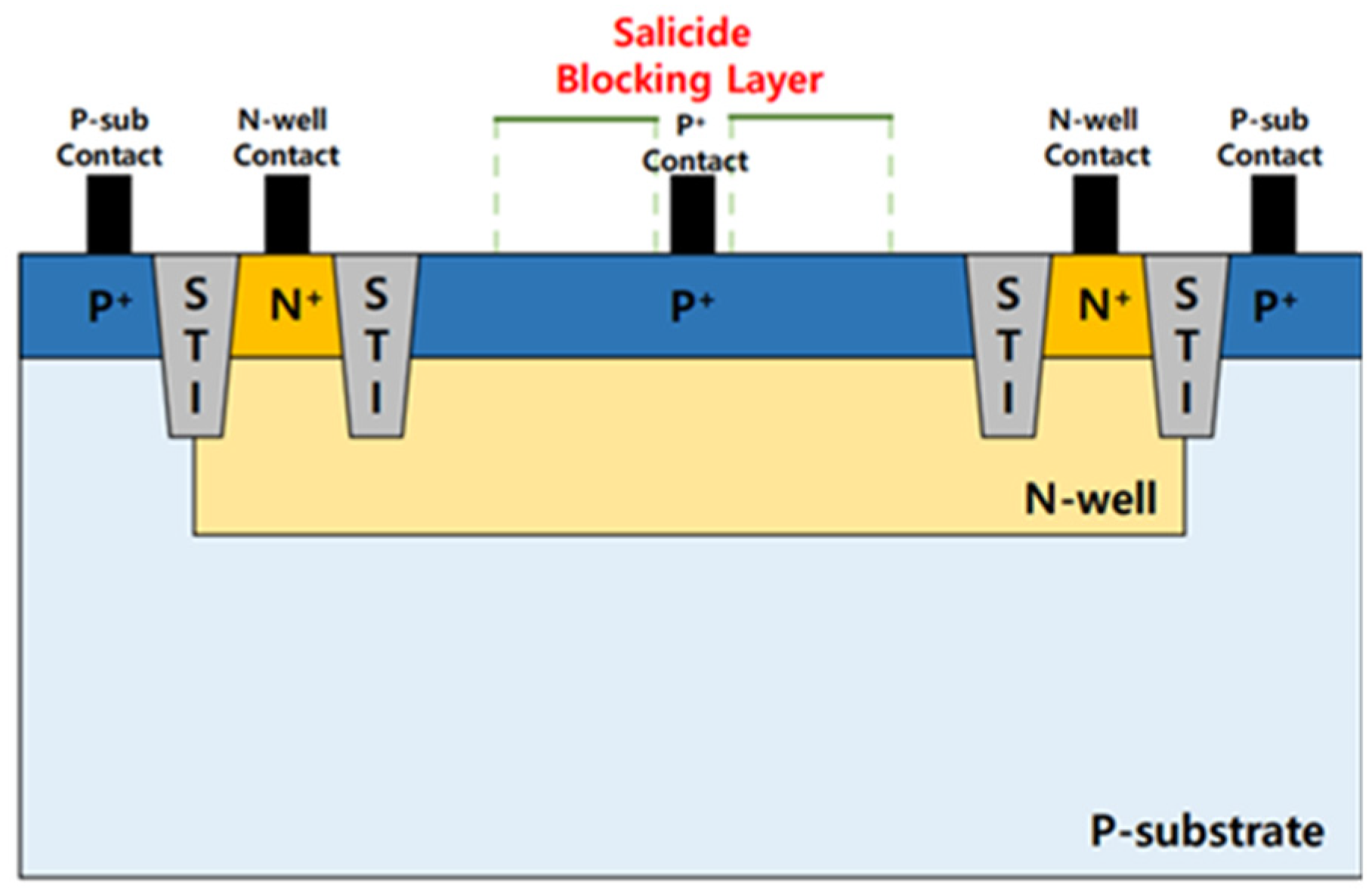
Figure 2 illustrates the cross-sectional view of the on-chip CMOS P+/NW APD formed by a P+/NW junction and an NW/P-substrate junction. Here, the avalanche multiplication is initiated by a hole in the P+/NW junction [4,5]. The P+ contacts shown in the mid-region are connected to the front-end TIA, thereby excluding the slow diffusion currents contributed from the P-substrate, and thus providing the characteristics of high responsivity and large bandwidth. Additionally, shallow trench isolation (STI) is located between two active areas as guard rings and penetrates deeper than the P+/NW junction. Then, the electric field can be distributed uniformly at the edge of the junction. Therefore, the STI can prevent premature edge breakdown, although it may decrease the responsivity of the P+/NW APD [6]. The P+ source and drain regions should be covered by the salicide blocking layer to form an optical window. Yet, the P+ contacts should be open because the salicidation process reduces the contact’s resistivity [7]. In addition, the area occupied by the P+ contacts should be small enough not to degrade the responsivity.

2.2. P+/Deep N-Well APD

Figure 3 shows the cross-sectional view of the on-chip CMOS APD based on the P+/DNW junction, where the slow diffusion currents from the P-substrate are eliminated by using a DNW. Hence, the near-infrared (NIR) sensitivity can be greatly improved because the depletion region is formed deeper and wider than other structures. However, it should be noted that the premature edge breakdown might occur, provided that the depletion region is formed way below STI. Furthermore, the responsivity is considerably lower than in other structures, which is confirmed by the measured results.

2.3. P+/N-Well/Deep N-Well APD

Figure 4 illustrates the cross-sectional view of the on-chip CMOS P+/NW/DNW APD, where the avalanche multiplication is also initiated by a hole at the P+/NW junction. The premature edge breakdown can be prevented by the STIs. Additionally, the addition of a DNW improves the NIR sensitivity because it decreases the number of holes spreading into the P-substrate. Moreover, the photocurrents generated in the P-substrate can be excluded, owing to the built-in potential barrier between the DNW and the P-substrate.
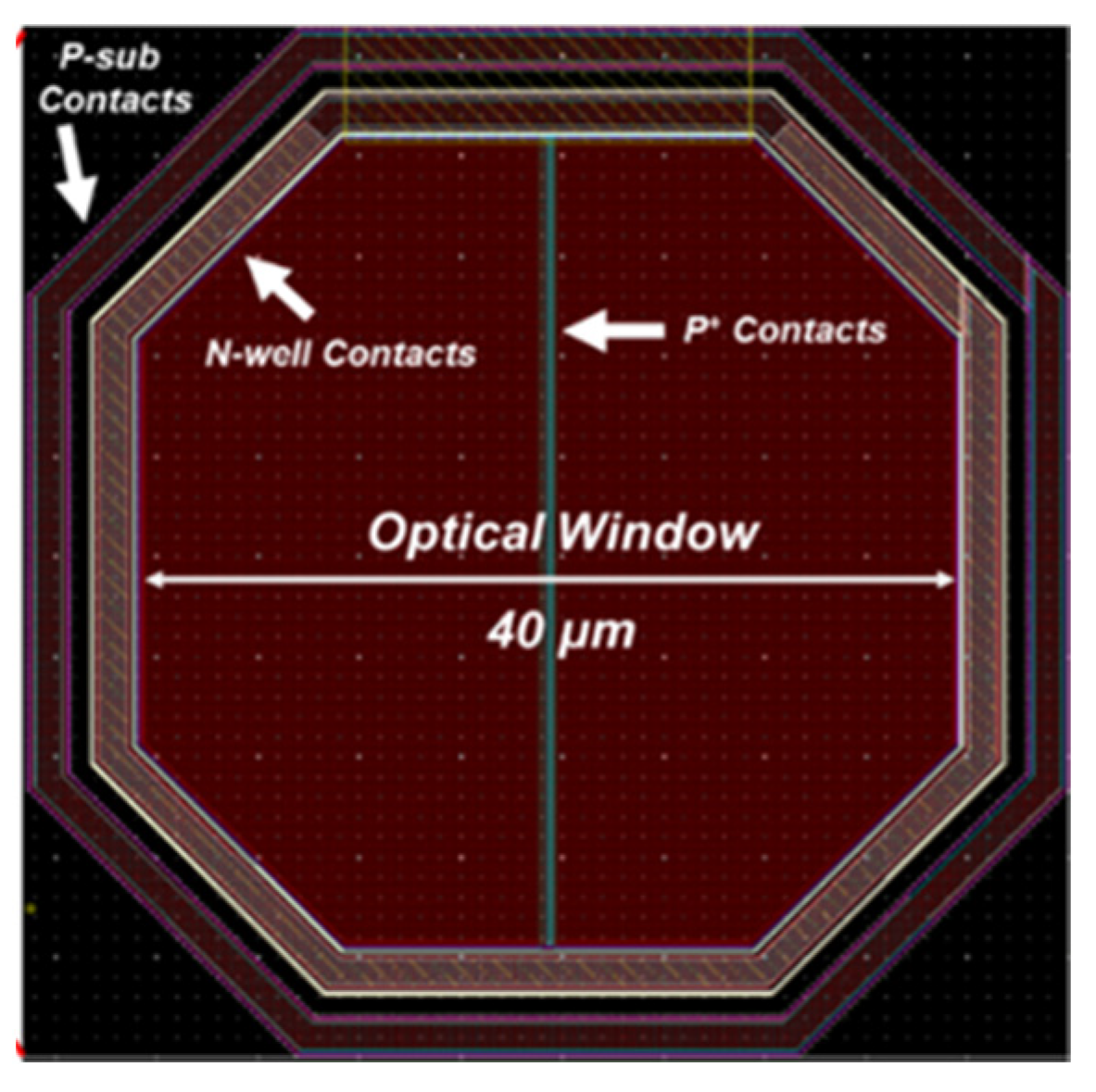
Figure 5 depicts the layout of an on-chip CMOS APD, where the P+ source and drain regions should be covered by the salicide blocking layer to form an optical window. However, the P+ contacts in the middle of the optical window should not be blocked because the salicidation process reduces the contact’s resistivity [6]. The diagonal length of the optical window is 40 µm, such that the APD provides a total depletion capacitance (CPD) of 490 fF and a photodetection bandwidth of 1.7 GHz at the reverse bias of 10.25 V. The octagonal shape is preferred to minimize the feasible damage from the edge breakdown. For HSPICE simulation purposes, the equivalent modeling of the on-chip APD comprises an ideal current source with a parasitic capacitance of 490 fF.

2.4. Measured Results

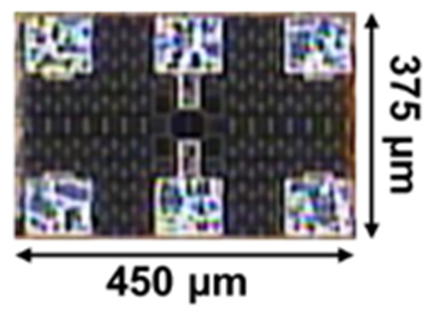
These three types of on-chip APDs were implemented by using a TSMC 0.18 μm 1P6M RF CMOS process. Figure 6 shows an example of chip photographs for three on-chip APDs, where each area occupies 375 × 450 μm2, including I/O pads.
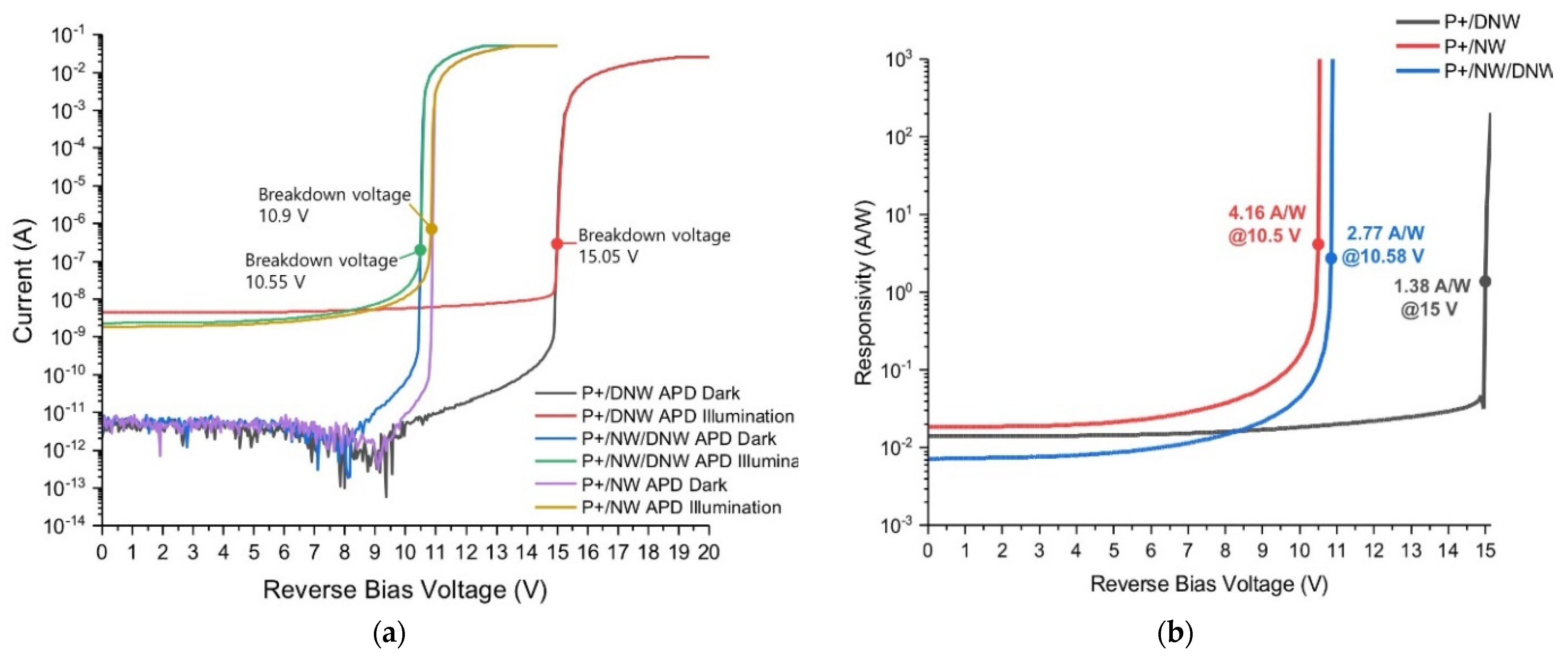
Figure 7 and Figure 8 demonstrate the measured current-voltage (I–V) characteristics of each APD and the measured responsivity versus the reverse bias voltages under the conditions of both dark and optical illuminations. It is clearly seen that both the dark current and the illumination current increase dramatically at the breakdown voltage due to the avalanche multiplication process.
The breakdown voltages are measured to be 10.9 V for P+/NW APD, 15.05 V for P+/DNW APD, and 10.55 V for P+/NW/DNW APD, respectively. Here, the inserted optical power (Popt) was set to −30 dBm. Then, the responsivity (R) of each APD is estimated by,
R = I i l l u m i n a t i o n I d a r k P o p t ,
where Popt is the incident optical power, and Iillumination and Idark represent the measured currents under the illumination and the dark conditions.
Additionally, it is clearly seen that the measured responsivity is 2.77 A/W at 10.85 V for P+/NW APD, 1.38 A/W at 15 V for P+/DNW APD, and 4.16 A/W at 10.5 V for P+/NW/DNW APD, respectively.

3. Voltage-Mode Optoelectronic Receiver (V-OER)

3.1. Experimental Methods

An optoelectronic optical receiver IC with the suggested on-chip APDs was realized in a TSMC 180 nm CMOS process to verify the feasibilities for the applications of short-range LiDAR sensors. As a front-end transimpedance amplifier (TIA), a conventional voltage-mode feedforward input circuit (VFIC) is exploited in this work since it can provide low-noise high-gain performance [5]. Figure 8 shows the block diagram of the voltage-mode optoelectronic receiver (V-OER) which consists of an APD as an optical detector, a VFIC as a TIA to convert the generated photocurrents to electrical voltages, a single-to-differential (S2D) converter for differential signaling, a differential gain stage for gain boosting, and a cross-coupled inverter post-amplifier (CI-PA) for offset cancellation. An output buffer (OB) is inserted not only for 50 Ω impedance matching, but also for the effective isolation of the V-OER circuit from the following time-to-digital converter (TDC) that is typically employed to estimate the time interval between the transmitted pulses and the received echo pulses [9,10].
In the VFIC, a voltage-mode inverter (INV) input stage with a feedback resistor (RF) is merged with a feedforward common-source amplifier of which the gate node is connected to the gates of the INV input stage [4,5]. The CI-PA consists of four inverters and two diode-connected output buffers, where the output voltages (VON and VOP) can be enhanced by merging the input signals (OUTN and OUTP) with other small portions of another path. However, circuit designs should be carefully conducted to match g m n / v g s with g m p / v g s because the amplitude mismatches between two outputs might occur in the cases of short-distance detection, where gmn and gmp represent the transconductance of NMOS and PMOS transistors, respectively.

3.2. Measured Results

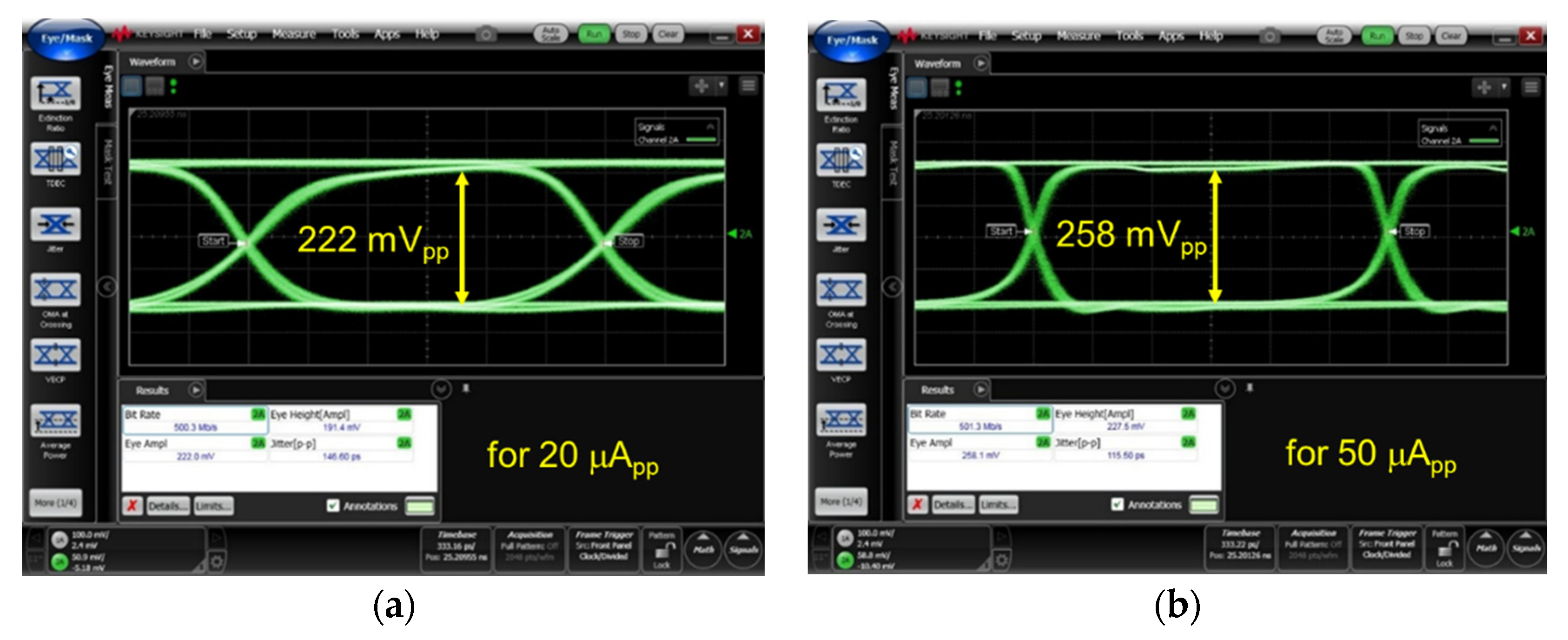
Firstly, the implemented V-OER IC demonstrated the electrically measured eye-diagrams, where the eyes of the V-OER IC were wide and clean at a data rate up to 500 Mb/s with the input currents of 20 μApp and 50 μApp, respectively. The single-ended output amplitude of each eye-diagram was measured with a 50 Ω termination, where amplitudes acquired were similar to those demonstrated in [5].
Secondly, the electrically measured output noise of the V-OER IC revealed that the equivalent noise current spectral density was 4.54 pA / Hz , which corresponds to the optical sensitivity of −35.5 dBm for the BER of 10−12 with the APD responsivity of 2.77 A/W. Here, it is noted that the inherent noise voltage of the utilized oscilloscope (i.e., Agilent DCA 86100D) was measured to be 0.75 mVRMS.
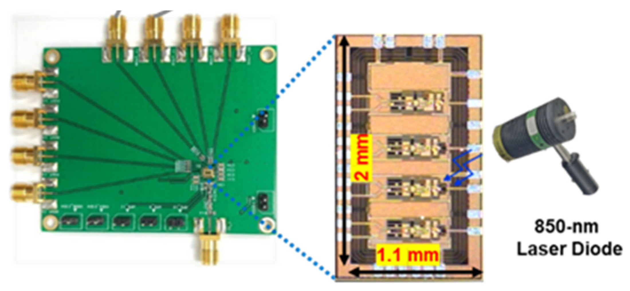
Figure 9 depicts a PC-board module for optical testing, in which on-chip APDs were integrated on the same die of the V-OER IC. The four-channel V-OER array IC occupies the total area of 2.0 × 1.1 mm2, including I/O pads. For optical testing, an 850 nm laser source driver (Seed LDD, Notice Korea Ltd., Anyang, Republic of Korea) with a laser diode (Qphotonics, Ann Arbor, MI, USA) was utilized to generate light pulses.
Figure 10 demonstrates the electrically measured eye-diagrams of the V-OER at 500 Mb/s with different input currents of 20 μApp and 50 μApp, in which a singled-ended output was measured with a 50 Ω termination. Hence, each output corresponds to the transimpedance gain of 91.6 dBΩ and 85.2 dBΩ, respectively.
Additionally, the output noise voltage of the V-OER IC was measured with the inherent background noise of the oscilloscope (Agilent DCA 86100D). Thereby, the input-referred average noise current spectral density is estimated to 4.54 pA / Hz , which corresponds to the optical sensitivity of −29.5 dBm for bit-error-rate (BER) of 10−12 to satisfy the maximum signal-to-noise ratio (SNR) of 14.
Figure 11 demonstrates the optically measured pulse responses, where the light pulses were generated by utilizing an 850 nm laser source driver. It is clearly seen that the V-OER IC with the P+/NW/DNW APD yields the largest output pulses.
Table 1 compares the performance of the realized V-OER IC with the prior parts for the applications of short-range LiDAR sensors. Ref. [4] demonstrated an optoelectronic receiver IC for home-monitoring purposes, which consisted of an on-chip P+/NW APD, a feedforward TIA, and a limiting amplifier. However, the measured results showed poorly recovered optical pulses, i.e., 8 mVpp amplitude with a 25 ms pulse width. Ref. [11] suggested a differential shunt-feedback (SF) TIA employing an off-chip APD (with 40-A/W responsivity). Even though it achieved very high transimpedance gain and a very large maximum detectable input current, AC coupling capacitors and bias resistors were mandatory for the interconnection between the off-chip APD and the receiver. Additionally, it required a separate TDC IC so that the maximum input dynamic range could be achieved. Ref. [12] presented a frequency-compensated inverter TIA that could demonstrate very-low-noise current spectral density. However, it revealed high power dissipation and mandated a large reverse voltage of 200 V for the off-chip APD to achieve 50 A/W responsivity characteristics. Ref. [13] realized a shunt-feedback (SF) TIA with an off-chip APD, providing a very low-power solution. Furthermore, it could recover a narrow pulse width of 2 ns. Yet, the chip area was quite large.
The V-OER IC exploits an on-chip APD to realize a small chip area and provide a low minimum detectable current and a large signal-to-noise ratio (~10 in this work). However, it is clearly seen that the input dynamic range is very limited—to 26.4 dB (i.e., the max. input current of 50 μApp).

4. Proposed Current-Mode Optoelectronic Receiver (C-OER)

Voltage-mode TIAs can be preferred for long-range LiDAR sensors because of their low-noise characteristics. In particular, inverter TIAs (INV-TIAs) have been frequently exploited because of their inherent advantages such as easy design, no additional bias circuitry, high gain, low noise, etc. However, they may suffer from considerable degradation of bandwidth and noise performance because the photodiode capacitance (Cpd) may vary significantly depending upon the amplitudes of the incoming input currents [10]. Hence, we employ a current-mode TIA in this work as a front-end circuit to facilitate the aforementioned issues of the photodiode capacitance.
Basically, a current-mode TIA functions as a current-buffer, provides a small input resistance, and thus helps to isolate the photodiode capacitance from the determination of the circuit bandwidth. Common-gate architecture is a conventional example of a current-mode TIA, which however suffers from the significant loss of currents because the input resistance (~1/gm) cannot be indefinitely reduced [10]. To the contrary, the symmetric current-conveyor input buffer (CCIB) architecture is another example of a current-mode TIA, which can prevent the loss of input currents effectively since the modified cascode input configuration yields a large output resistance.
Figure 12 illustrates the block diagram of the proposed current-mode optoelectronic receiver (C-OER), which consists of an on-chip APD to generate photocurrents, a parallel arrangement of five current conveyor input buffers (CCIBs) that can separate the parasitic photodiode capacitance from the cascode inverter stage (CIS) effectively, a single-to-different (S2D) converter for differential signaling to improve common-mode rejection ratio characteristics, a second-stage differential amplifier (DIFF) for further gain-boosting and improved output symmetry, a cross-coupled inverter-based post-amplifier (CI-PA) to boost the output swing and reduce the mismatches between differential pulses, and an output buffer (OB) for 50 Ω impedance matching.
Figure 13a depicts the schematic diagram of a single CCIB stage with a modified NMOS cascode circuit (M1~M4) incorporated into its PMOS counterpart (M5~M8). Consequently, half (i.e., iPD,n) of the input current flows through the NMOS cascode circuit (M1 and M2), while the other half (i.e., iPD,p) flows into the PMOS cascode circuit (M5 and M6). Therefore, the total input photocurrent (iPD) from the photodiode can be almost symmetrically split into two paths. Furthermore, the two currents (iPD,n and iPD,p) are mirrored to the circuit, comprising M3, M4, M7, and M8. The mirrored currents can be summed and flow out of the feedback resistor (RF) in the following CIS. Consequently, a positive transimpedance gain can be provided, which is the opposite to the case of the previous V-OER.
According to small signal analysis, the input resistance of the CCIBs varies with respect to the number of the switched-on blocks. When only CCIB#3 is turned on, the input resistance (Rin,3) is given by,
R i n , 3 = 1 g m 2 | | 1 g m 5 1 2 g m ,
where gm2 and gm5 represent the transconductance of M2 and M5, respectively. Provided that gm2 = gm5 = gm, the input resistance becomes equal to 1/2gm.
When other two CCIB blocks (#2 and #4) are added to CCIB#3 with the switch turned on, the new input resistance (Rin,2) is given by,
R i n , 2 = R i n , 3 | | R i n , p a r a l l e l 1 2 g m | | 1 2 g m | | 1 2 g m = 1 6 g m
All the CCIB blocks are turned on simultaneously, the input resistance (Rin) is given by,
R i n = R i n , 2 | | R i n , p a r a l l e l 1 6 g m | | 1 2 g m | | 1 2 g m = 1 10 g m
Therefore, it is clearly seen that the CCIB stage provides a very low input resistance of 1/10gm, hence helping to isolate the photodiode capacitance from the bandwidth determination more effectively than the V-OER. Additionally, it yields a large output resistance of ~(1/2)gmro2, thereby preventing the loss of the input current signals more efficiently.
Figure 13b shows the schematic diagram of the cascode inverter stage (CIS) with a feedback resistor array (FRA) that comprises five resistors (RF1~RF3) and four switches (M17~M20). The FRA conducts the function of automatic gain control (AGC). Among the five resistors in the FRA, RF1 should always be connected, while the other four resistors (RF2 and RF3) are turned on via thick-gate NMOS switches (M17~M20). These thick-gate NMOS switches are designed to operate in pairs and are controlled by a feedforward voltage generator (FVG) that consists of two-stage cascaded amplifiers and an on-chip MIM capacitor (CMIM) for low-pass filtering, as shown in Figure 13c. Thereby, the transimpedance gain can be tuned automatically within the duration of a narrow single pulse at the different input voltages of VB1 and VB2, respectively.
Based on the output voltage (IB_OUT) of the CCIB stage, the FVG generates 3.3 V DC voltages (FVG_OUT) to turn the NMOS switches on in the FRA. When the FVG turns all the NMOS switches on, the CIS produces the lowest transimpedance gain. When the FVG is turned off, only the feedback resistor RF1 is activated and thus the CIS amplifies the input currents with the highest transimpedance gain.
Small signal analysis indicates that the transimpedance gain of the CIS is given by,
Z T , i n v A i n v 1 + A i n v R F , E Q R F , E Q ,
where Ainv is the voltage gain of the CIS, and RF,EQ represents the equivalent feedback resistance of the FRA [10].
The input resistance of the CIS is given by,
R i n , I T S = R F A i n v + 1 R F , t o t g m 2 r o 2 ,
where the non-dominant pole occurs at the input node of the CIS. The output pole also becomes non-dominant because of its small capacitance [10]. Therefore, the bandwidth (f-3dB) is nearly determined at the input node of the CCIB stage, i.e.,
f 3 d B 1 10 π R i n ( C p d + 2 C g s , n + 2 C g s , p ) ,
where Rin is the input resistance of the CCIB stage as defined in (3), Cpd is the photodiode capacitance, Cgs,n is the gate-source capacitance of NMOS transistors (M2 and M4), and Cgs,p is the gate-source capacitance of PMOS transistors (M5 and M7), respectively [10].
The input-referred equivalent noise current spectral density of the five CCIB blocks is roughly given by,
i 2 e q 5 i 2 d 2 + i 2 d 5 + i 2 d 4 + i 2 d 7 g m 4 2 · ω 2 C t o t 2 + ω 2 C t o t 2 5 g m 4 2 · i 2 R F , E Q + i 2 d 16 + i 2 d 13 g m 16 2 · 1 R F , E Q 2 + ω 2 C 1 2 ,
where i 2 d i i = 2,4 , 5,7 represents the thermal noise current spectral density of Mi (i=2,4,5,7), i 2 R F , t o t is the thermal noise current of RF,EQ, C 1 ( = C g s 13 + C g s 16 ) is the input capacitance of the CIS, and C t o t ( = 5 C i n + C p d ) represents the total capacitance at the input node of the CCIB that comprises the input capacitance C i n = C g s 2 + C g s 4 + C g s 5 + C g s 7 of the CCIB and the photodiode capacitance (Cpd).
Here, it is assumed that gm2 = gm5, gm4 = gm7, gm13 = gm16, i 2 d 2 = i 2 d 5 , i 2 d 4 = i 2 d 7 , and i 2 d 13 = i 2 d 16 . Therefore, Equation (7) is simply approximated by,
i 2 e q 10 i 2 d 2 + ω C t o t g m 4 2 10 i 2 d 4 + i 2 R F , E Q 5 + 2 i 2 d 16 5 · ω C 1 g m 16 2 = 40 K T Γ g m 2 + 8 K T Γ ω C t o t g m 4 2 5 g m 4 + 1 10 Γ R F , E Q + g m 16 5 2 ω ω T 2 40 K T Γ g m 2 + ω 2 C t o t 2 g m 4
where K is the Boltzmann constant, T is the absolute temperature, Γ is the noise factor of MOSFET. Under the assumption that gm2 = gm4, the input capacitance ( C i n ) should be roughly equal to ( C p d 5 ) to minimize the noise current spectral density.
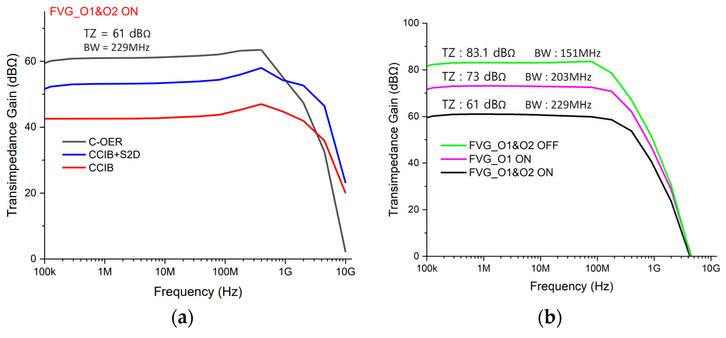
Post-layout simulations were performed for the proposed C-OER by using the model parameters of a TSMC 180 nm CMOS technology. Figure 14a shows the frequency response with the FVG modules turned on, achieving the transimpedance gain of 61 dBΩ and the bandwidth of 229 MHz. Figure 14b illustrates that the C-OER obtains the transimpedance gain of 73 dBΩ and a bandwidth of 203 MHz when only the FVG_O1 module is turned on. The largest transimpedance gain of 83.1 dBΩ and a bandwidth of 151 MHz are obtained when the FVGs are turned off.
Figure 15 depicts the simulated pulse responses of the C-OER at different input current levels of 5 μApp~1.0 mApp, which corresponds to the input dynamic range of 46 dB. Moreover, it is clearly seen that the output voltages can be saturated with the input currents of 300 μApp and above.

5. Measured Results of the Proposed C-OER

5.1. Experimental Methods

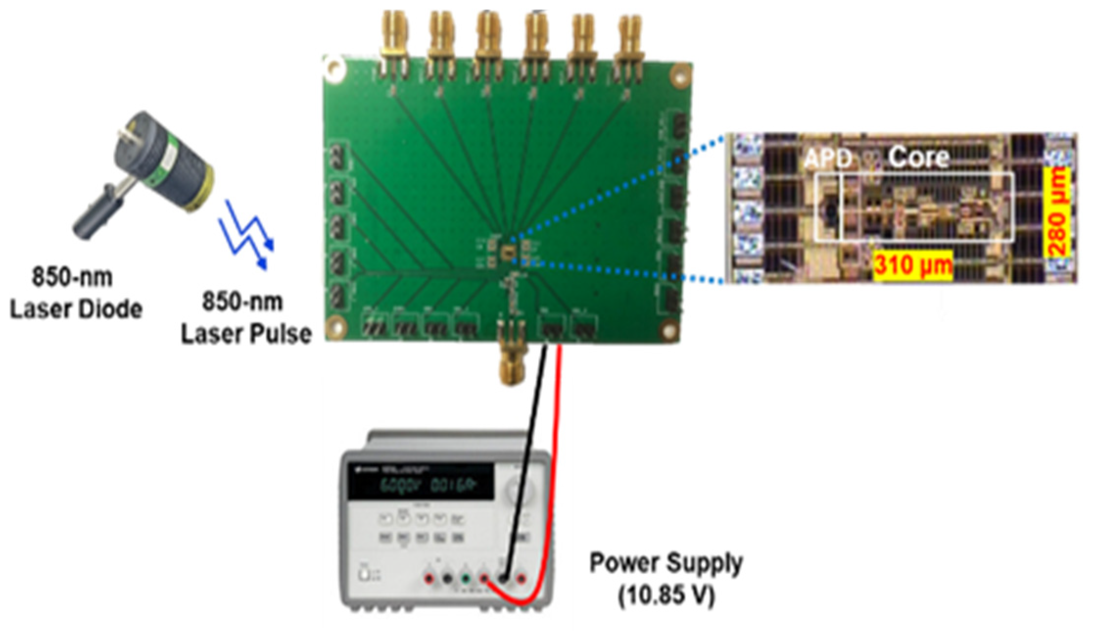
Test chips of the proposed C-OER IC were implemented in the same CMOS process. Figure 16 depicts the chip photograph of the C-OER IC and a PC-board module for optical testing, where an 850 nm laser source driver (Seed LDD, Notice Korea Ltd., Anyang-si, Republic of Korea) with a laser diode (Qphotonics, Ann Arbor, MI, USA) was utilized to generate light pulses. The chip core occupies the area of 0.087 mm2, and the DC measurements reveal the power dissipation of 47.8 mW from a 1.8 V supply.

5.2. Measured Results

Figure 17 demonstrates the optically measured pulse responses of the proposed C-OER IC for two different on-chip APDs with two different input pulses, where it is clearly seen that the C-OER integrated with the P+/NW APD exhibits relatively much larger output voltages than the case with the P+/DNW APD. Here, it is noted that the P+/NW/DNW APD was not integrated in this C-OER IC even with its highest responsivity because this might saturate the output voltages even at a much smaller input current than 1 mApp, i.e., the limited input dynamic range.
Therefore, the P+/NW APD would be the most appropriate detector, not only to extend the input dynamic range further, but also to recover the weak input currents of 5 μApp well enough.
Table 2 compares the performance of the C-OER IC with the previously reported CMOS receivers for short-range LiDAR sensors. Ref. [14] suggested a current-mirror (CM) input configuration with a shunt-feedback (SF) topology, which could successfully attain high transimpedance gain and wide dynamic range. However, the AGC function was carried out by an external field programmable gate array (FPGA). Ref. [15] merged a voltage-mode feedforward input configuration with a negative feedback AGC circuit comprising four switches so as to extend the dynamic range. However, it exploited off-chip APDs and the AGC circuit could not recover the input pulses within a single-pulse width. Ref. [16] proposed a capacitive feedback (CF) topology to obtain nanoampere low-noise currents. However, the manual gain control was required for low-gain and high-gain modes, and the maximum current detectable in the loop was limited to 250 μApp. Ref. [17] achieved a wide bandwidth with a current-amplifier-based feedback configuration (CAF) by a pole-zero cancellation technique. Nevertheless, the AGC function was conducted by using an external control. Yet, the detectable current range was limited from 23 μApp to 83 μApp.
In this proposed C-OER IC, we have realized the variable AGC mechanism within a narrow single-pulse width by employing FRA feedforward gain control. Consequently, the input dynamic range is extended much further than the V-OER, i.e., the maximum and minimum detectable currents of 1 mApp, and 5 μApp, respectively.

6. Conclusions

We have demonstrated the realization of a conventional voltage-mode optoelectronic receiver (V-OER) with three different on-chip APDs by utilizing a TSMC 180 nm RF CMOS process in order to confirm the feasibility of the CMOS on-chip APDs. However, the V-OER IC showed the inherent characteristics of the limited dynamic range. Then, we have presented the C-OER IC, in which a current-conveyor input buffer was employed to deliver the input photocurrents with no loss and to acquire a positive transimpedance gain with automatic gain control within a narrow single-pulse width. Implemented in the same TSMC 180 nm CMOS process, the optically measured results demonstrate the vividly large output pulses and conclusively confirm that the proposed C-OER provides a highly efficient solution for short-range LiDAR sensors.

Author Contributions

Conceptualization, S.-M.P.; methodology, J.-E.J., M.-J.L. and S.-M.P.; validation, Y.H., J.-E.J. and M.-J.L.; writing—original draft preparation, Y.H., J.-E.J. and S.-M.P.; writing—review and editing, X.Z., Y.C., S.C., J.-E.J., M.-J.L. and S.-M.P.; visualization, Y.H., J.-E.J., Y.C. and S.C.; supervision, S.-M.P.; project administration, S.-M.P.; funding acquisition, S.-M.P. All authors have read and agreed to the published version of the manuscript.

Funding

This work was supported by the National Research Foundation of Korea (NRF) grant funded by the Korea government (MSIP) (No. 2020R1A2C1008879). Additionally, this research was supported by the MSIT (Ministry of Science and ICT), Korea, under the ITRC (Information Technology Research Center) support program (IITP-2020-0-01847) supervised by the IITP (Institute for Information and Communications Technology Planning and Evaluation). In addition, this work was supported by the National Research Foundation (NRF), Korea, under project BK21 FOUR. The EDA tool and chip fabrication were supported by the IC Design Education Center.

Institutional Review Board Statement

Not applicable.

Informed Consent Statement

Not applicable.

Data Availability Statement

Not applicable.

Acknowledgments

The EDA tool and chip fabrication were supported by the IC Design Education Center.

Conflicts of Interest

The authors declare no conflict of interest.

References

  1. Han, J.; Choi, B.; Seo, M.; Yun, J.; Lee, D.; Kim, T.; Eo, Y.; Park, S.M. A 20-Gb/s Transformer-Based Current-Mode Optical Receiver in 0.13-μm CMOS. IEEE Trans. Circuits Syst. II Express Briefs 2010, 57, 348–352. [Google Scholar]
  2. Lee, D.; Han, J.; Han, G.; Park, S.M. An 8.5-Gb/s fully integrated CMOS optoelectronic receiver using slope-detection adaptive equalizer. IEEE J. Solid-State Circuits 2010, 45, 2861–2873. [Google Scholar] [CrossRef]
  3. Zimmermann, H.; Heide, T. A monolithically integrated 1-Gb/s optical receiver in 1-μm CMOS technology. IEEE Photonics Technol. Lett. 2001, 13, 711–713. [Google Scholar] [CrossRef]
  4. Joo, J.-E.; Lee, M.-J.; Park, S.M. A CMOS optoelectronic receiver IC with an on-chip avalanche photodiode for home-monitoring LiDAR sensors. Sensors 2021, 21, 4364. [Google Scholar] [CrossRef] [PubMed]
  5. Hu, Y.; Joo, J.-E.; Lee, M.-J.; Park, S.M. An Optoelectronic Transimpedance Amplifier in 180-nm CMOS for Short-range LiDAR Sensors. J. Semicond. Technol. Sci. 2022, 22, 275–281. [Google Scholar] [CrossRef]
  6. Lee, M.-J.; Choi, W.-Y. Performance comparison of two types of silicon avalanche photodetectors based on N-well/P-substrate and P+/N-well junctions fabricated with standard CMOS technology. J. Opt. Soc. Korea 2011, 15, 1–3. [Google Scholar] [CrossRef] [Green Version]
  7. Lee, M.-J.; Choi, W.-Y. Effects of parasitic resistance on the performance of silicon avalanche photodetectors in standard CMOS technology. IEEE Electron Device Lett. 2015, 37, 60–63. [Google Scholar] [CrossRef]
  8. Lee, M.-J.; Choi, W.-Y. Area-dependent photodetection frequency response characterization of silicon avalanche photodetectors fabricated with standard CMOS technology. IEEE Trans. Electron Devices 2013, 60, 998–1004. [Google Scholar] [CrossRef]
  9. Park, Y.; Park, S.M. A dual-feedback folded-cascode fully differential transimpedance amplifier in 65-nm CMOS. J. Semicond. Technol. Sci. 2020, 20, 281–287. [Google Scholar] [CrossRef]
  10. Yoon, D.; Joo, J.-E.; Park, S.M. Mirrored Current-Conveyor Transimpedance Amplifier for Home Monitoring LiDAR Sensors. IEEE Sens. J. 2020, 21, 5589–5597. [Google Scholar] [CrossRef]
  11. Kurtti, S.; Jansson, J.-P.; Kostamovaara, J. A CMOS receiver–TDC chip set for accurate pulsed TOF laser ranging. IEEE Trans. Instrum. Meas. 2019, 69, 2208–2217. [Google Scholar] [CrossRef] [Green Version]
  12. Wang, X.; Ma, R.; Li, D.; Zheng, H.; Liu, M.; Zhu, Z. A low walk error analog front-end circuit with intensity compensation for direct ToF LiDAR. IEEE Trans. Circuits Syst. I Regul. Pap. 2020, 67, 4309–4321. [Google Scholar] [CrossRef]
  13. Zheng, H.; Ma, R.; Liu, M.; Zhu, Z. A linear-array receiver analog front-end circuit for rotating scanner LiDAR application. IEEE Sens. J. 2019, 19, 5053–5061. [Google Scholar] [CrossRef]
  14. Zheng, H.; Ma, R.; Liu, M.; Zhu, Z. High Sensitivity and Wide Dynamic Range Analog Front-End Circuits for Pulsed TOF 4-D Imaging LADAR Receiver. IEEE Sens. J. 2018, 18, 3114–3124. [Google Scholar] [CrossRef]
  15. Hong, C.; Kim, S.-H.; Kim, J.-H.; Park, S.M. A linear-mode LiDAR sensor using a multi-channel CMOS transimpedance amplifier array. IEEE Sens. J. 2018, 18, 7032–7040. [Google Scholar] [CrossRef]
  16. Cho, H.-S.; Kim, C.-H.; Lee, S.-G. A high-sensitivity and low-walk error LADAR receiver for military application. IEEE Trans. Circuits Syst. I Regul. Pap. 2014, 61, 3007–3015. [Google Scholar] [CrossRef]
  17. Chen, R.Y.; Yang, Z.-Y. CMOS transimpedance amplifier for gigabit-per-second optical wireless communications. IEEE Trans. Circuits Syst. II Express Briefs 2015, 63, 418–422. [Google Scholar] [CrossRef]
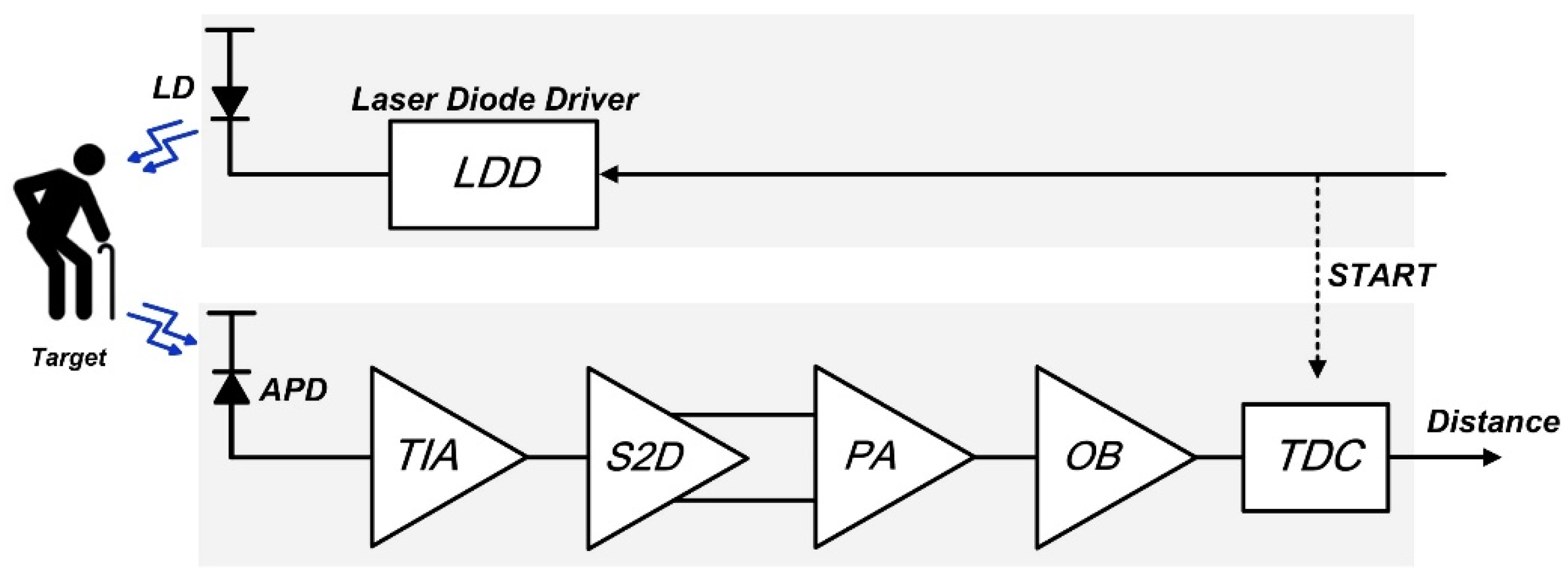
Figure 1. Block diagram of a typical LiDAR sensor.
Photonics 10 00746 g001
Figure 2. Cross-sectional view of a P+/NW APD [4,5].
Photonics 10 00746 g002
Figure 3. Cross-sectional view of a P+/DNW APD.
Photonics 10 00746 g003
Figure 4. Cross-sectional view of a P+/NW/DNW APD.
Photonics 10 00746 g004
Figure 5. Layout of an on-chip APD.
Photonics 10 00746 g005
Figure 6. An example of on-chip APDs’ photograph.
Photonics 10 00746 g006
Figure 7. (a) Measured I-V curves and (b) Measured responsivities of the three on-chip APDs.
Photonics 10 00746 g007
Figure 8. Block diagram of the voltage-mode optoelectronic receiver (V-OER) with an on-chip APD.
Photonics 10 00746 g008
Figure 9. Chip photo of the V-OER IC in a test module with three CMOS APDs.
Photonics 10 00746 g009
Figure 10. Electrically measured eye-diagrams of the V-OER for 223-1 PRBS input currents at 500-Mb/s data rates: (a) 20 μApp and (b) 50 μApp, respectively.
Photonics 10 00746 g010
Figure 11. Optically measured pulse responses of the V-OER with three different APDs for (a) 5 ns and (b) 50 ns input pulses, respectively.
Photonics 10 00746 g011
Figure 12. Block diagram of the proposed C-OER.
Photonics 10 00746 g012
Figure 13. Schematic diagrams and the specific parameters of (a) CCIB, (b) CIS, and (c) FVG blocks.
Photonics 10 00746 g013
Figure 14. Simulated gain variations (a) with both FVGs turned on, (b) with FVG turn on and off, respectively.
Photonics 10 00746 g014
Figure 15. Simulated pulse responses of the proposed C-OER IC: (a) with small (5~100 μApp), (b) with large (0.2~1 mApp) input currents, respectively.
Photonics 10 00746 g015
Figure 16. Chip photo of the C-OER IC and its test module.
Photonics 10 00746 g016
Figure 17. Optically measured pulse responses of the proposed C-OER IC with two different APDs for (a) 50 ns and (b) 100 ns input pulses.
Photonics 10 00746 g017
Table 1. Performance comparison with previously reported voltage-mode CMOS TIAS.
PARAMETERS[4][11][12][13]V-OER
CMOS technology (nm)180350180180180
APDOn-chipOff-chipOff-chipOff-chipOn-chip
Input configurationVCFSFSF with FCSFVCF
Bandwidth (MHz)790230281450608
TZ gain (dBΩ)93.41008610095.1
Noise current spectral density (pA/sqrt(Hz))126.324.682.594.54
Min. detectable current (mApp)6.74
(SNR = 10)
1.0
(SNR = 5)
2.0
(SNR = 25)
2.5
(SNR = 5)
2.38
(SNR = 10)
Single-pulse width25 ms3 ns3 ns2 ns5 ns
Optically measured pulse (mVpp)8200110300200
Power dissipation (mW)56.5 (w/OB)180 (w/TDC)200 (w/PA)6.6 (w/o OB)39.3 (w/OB)
Core area (mm2)0.09142.204.080.068
VCF: voltage-mode CMOS feedforward, SF: shunt feedback, FC: frequency compensation, SNR: signal-to-noise ratio.
Table 2. Performance Comparison with Previously Reported CMOS Receivers for LiDAR Sensors.
PARAMETERS[14][15][16][17]V-OERC-OER
CMOS technology (nm)180180350180180180
Supply (V)3.31.83.31.8/3.31.81.8/3.3
APDOn-chipOff-chipOn-chipOff-chipOn-chipOn-chip
Input configurationCM + SFVCFCFCAFVCFCCIB
Output signalingsingle-endeddifferentialsingle-endeddifferentialdifferentialdifferential
Bandwidth (MHz)1537201601000608151~229
TZ gain (dBΩ)10676.378~11056.8~69.395.161~83.1
Gain controlExternalAutoExternalExternalNoAuto
Max. detectable current (mApp)5.01.10.0220.0830.051.0
Min. detectable current (mApp)0.5
(SNR = 5)
1.14
(SNR = 12)
0.053
(SNR = 3.3)
23
(SNR = 14)
2.38
(SNR = 10)
5.0
(SNR = 14)
Power dissipation (mW)16.5(w/o OB)29.8796.6(w/o OB)39.3(w/OB)47.8
Core area (mm2)1.2 × 1.135.0 × 1.11.0 × 1.20.1 × 0.0750.0680.28 × 0.31
CM: current-mirror, CF: capacitive feedback.
Disclaimer/Publisher’s Note: The statements, opinions and data contained in all publications are solely those of the individual author(s) and contributor(s) and not of MDPI and/or the editor(s). MDPI and/or the editor(s) disclaim responsibility for any injury to people or property resulting from any ideas, methods, instructions or products referred to in the content.