1. Introduction
Terahertz (THz) waves are rays with a frequency range of 0.1–10 THz, the region of the electromagnetic spectrum between millimeter waves and infrared optics. [
1]. Research in THz technology has focused on detection, communication, and imaging. Due to the lack of efficient terahertz devices, the rich THz spectrum resources have not been fully exploited and have become a research hotspot in academia [
2,
3,
4,
5]. As one of the application devices of the THz system, the THz absorber has also attracted extensive attention from the scientific community and has become a key to promoting the application of THz technology [
6,
7].
In the field of THz electromagnetic waves, metamaterials are a new type of artificial composite electromagnetic material. The electricity, magnetic permeability, and permittivity of metamaterials can be controlled [
8,
9]. In recent years, utilizing the unique electromagnetic properties of metamaterials has become a new hotspot in the research of THz absorbers. Metamaterials break through and broaden the electromagnetic properties of existing materials in nature. Terahertz devices using metamaterials avoid the thickness limitation of traditional quarter-wavelength devices and greatly reduce the volume of devices. Their unique properties can effectively improve the performance of the THz absorber and even make it possible to design new breakthrough devices [
10,
11,
12].
Since the discovery of graphene [
13], 2D materials have become the star materials in the field of electromagnetic metamaterials, attracting the attention of scholars from all over the world. 2D materials such as graphene, MoS
2, and black phosphorus have unique electronic and optical properties and support surface plasmons, so they are widely used as metamaterials in THz absorbers [
14,
15,
16]. The 2D material is applied as a metamaterial for the absorber and can be used to provide flexible tunability. The frequency-selective surfaces can enhance the interaction between THz and 2D material atomic layers. At the same time, the tuneable characteristics of the 2D material can, in turn, control the resonant response of the frequency-selective surfaces. Thus, the 2D material and the frequency-selective surfaces are interacting and strengthening each other. 2D material absorbers are usually composed of subwavelength structural units, which are arranged in a certain way to achieve the modulation of electromagnetic waves. At present, 2D materials are used as metamaterials for absorbers, mainly in the form of monolayers or multilayers, such as monolayer–dielectric–monolayer–dielectric. In absorbers using monolayer 2D materials, most of them have multi-band characteristics [
17,
18,
19]. For example, the nanoribbon structure of graphene was used to achieve three absorption peaks in [
20]. In the absorbers of multilayered structures, some have broadband frequency characteristics and some have multi-band characteristics [
21,
22,
23,
24]. For example, a three-layered structure of graphene and TOPAS was used to achieve broadband absorption at 3.5 THz to 6 THz [
25]. In the literature [
26], a three-layered structure of graphene and TOPAS was also used to achieve three absorption peaks at 3 THz, 5 THz, and 7 THz, by corresponding to one resonance point per layer. Through multilayered 2D materials and dielectric materials, the absorbers can be matched with air impedance in a wider frequency range to obtain broadband characteristics. In this way, it can also match the air impedance at multiple frequency points to achieve multi-band characteristics. There are also fractal structures, which are useful for implementing multi-bands. Fractal element surfaces exhibit enhanced absorbance by increasing their order [
27,
28]. In the current study of multi-band absorbers of 2D materials, the distribution of peaks was mainly concentrated in the high frequency band of THz [
17,
20,
29,
30]. In addition, many absorbers used complex graphic structures, which increased the complexity of manufacturing.
Based on the current research status and demand for development, we adopted a new approach to designing metamaterial terahertz absorbers by stacking two two-dimensional materials. The material properties of the MoS2 and graphene-stacked structures were investigated. A complementary frequency-selective surface (FSS) structure was used for the absorber, and its equivalent circuit model was analysed. In addition, the effect of the absorber structure on performance was investigated through a series of numerical simulations. A comparative study of 2D materials with different layers and combinations was also carried out.
2. Structures and Theoretical Model
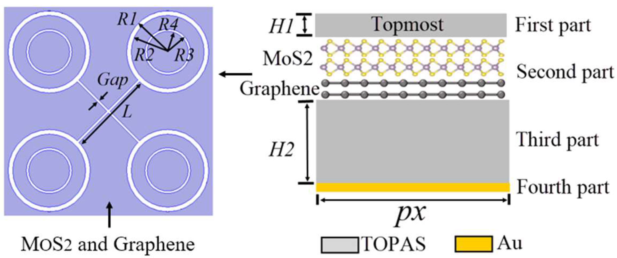
The unit cell of the MoS
2 and graphene-stacked structure absorber is presented in
Figure 1. The structure period is
px ×
px, where
px is the side length of the square unit. The THz absorber array consists of four parts. The first and third parts are made of thermoplastic olefin polymer of amorphous structure (TOPAS) material, with thickness values of
H1 and
H2. The second part is the metamaterial of the absorber. Unlike conventional 2D material absorbers, the second part is composed of 2 layers of MoS
2 stacked with 2 layers of graphene. The complementary frequency-selective surface consists of crossed linear slot units and circular slot units, and the multi-frequency characteristics are achieved by the coupling response between the different units. The detailed geometrical parameters are defined in
Figure 1. The fourth part is Au with a thickness of 1 µm, which functions as a reflecting layer.
The surface conductivity of 2D material consists of intra-band transition conductivity and inter-band transition conductivity, which is described by the Kubo equation model [
31].
In the THz band, the conductivity of the inter-band transition is close to zero due to the Pauli exclusion principle, and contributes little to the overall conductivity. Therefore, the 2D material conductivity equation can be approximated as the Drude model for metal. At room temperature (T = 300 K), the conductivity of MoS
2 (
) and graphene (
) can be expressed as:
where
i is an imaginary unit,
e is the electron charge, and
m* is effective electron mass. For n-type doped MoS
2,
m* = 0.53 m
e, and m
e is free electron mass. Intrinsic relaxation time of MoS
2 = 0.17 ps.
n is the carrier concentration; the value of
n can be adjusted by doping. In the paper,
n = 1 × 10
19 m
−2.
is the reduced Planck’s constant and
is the Fermi energy of graphene in Equation (3). As
n of MoS
2, the value of
also can be adjusted by doping. The Fermi energy of graphene
is set at 0.7 ev in the paper. Intrinsic relaxation time of graphene
= 1 ps.
The relative permittivity is the basic parameter of the absorbing material. In the THz band, the relative permittivity is a complex quantity; the real part represents the capacitance, and the imaginary part represents the loss. According to the previous Drude model, the relative permittivity of MoS
2 (
) and graphene (
) can be expressed, respectively, as:
where the monolayer thickness of MoS
2 = 0.65 nm and the monolayer thickness of graphene
= 0.35 nm.
is the dielectric constant in free space (
= 8.85 × 10
−12 F/m). According to Equations (4) and (5) and combined with the above parameters, the relative permittivity curves of MoS
2 and graphene were obtained (
Figure 2). From the comparison of the coordinates of the real part in the figure, it can be seen that the real part of the relative permittivity of MoS
2 was larger than that of graphene in the range of 1 THz. The imaginary parts of the relative permittivity of the two materials were relatively close. Different carrier concentrations and different Fermi energies had a greater impact on the relative permittivity of MoS
2 and graphene in the range of 1 THz. When greater than 2 THz, the real part of the relative permittivity of MoS
2 and graphene began to approach a constant value, while the imaginary part tended towards zero.
In the absorber structure of
Figure 1, different thicknesses of TOPAS material are used to cover the top and bottom of the 2D materials. TOPAS is a cyclic olefin copolymer (COC) resin, an ultra-pure and crystal-clear technical material. TOPAS (loss angle tangent of 0.00007) can maintain a constant refractive index and very small absorption at THz frequency. Therefore, TOPAS is very suitable as a dielectric substrate material for THz absorbers; the relative permittivity of TOPAS is 2.35 [
32]. Au is used as the substrate of the absorber; the relative permittivity of Au can be described using the Drude model. In the model, the plasma frequency of Au ω
p = 4.35 π × 10
15 rad/s and the collision frequency of Au γ = 3.19 π × 10
13 rad/s [
33].
The calculation of the absorber’s absorption is the total input energy minus the reflected output, and then minus the transmitted energy. Therefore, the absorption rate is: A = 1 − |S11|2 − |S21|2; S11 is the reflection parameter of the absorber, and S21 is the transmission parameter of the absorber. Since the thickness of Au is 1 μm, it is much thicker than skin depth. The Au substrate acts as a mirror to provide zero transmission. Therefore, the final absorption rate is A = 1 − |S11|2.
In general, the resonance characteristics of the metamaterial absorber can be analysed using equivalent circuit theory. The equivalent circuit was determined by the structural and electromagnetic parameters of the absorber.
Figure 3a depicts the distribution of the electromagnetic characteristics in the FSS plane of the absorber. The four capacitors (C01, C02, C03, and C04) were generated by the outer circular slots located at the corners of the cell. C05 was generated by the two crossed slot lines at the centre of the cell. Their values were all determined by the difference of
R1–
R2 and the width of the slots (
Gap), respectively. The equivalent inductance L0 in
Figure 3a was determined by the length of the contour of the entire structure, with a total length of (2π
R1 +
L) ×4. C1–C4 were the capacitive effects generated by the inner circular slot, which were affected by the difference of
R3–
R4. L1–L4 were the inductive effects generated by the inner ring. Their inductance values were related to the circumference of the inner ring (π
R2 + π
R3).
Figure 3b shows the overall equivalent circuit of the FSS. Since it was a complementary FSS structure, the capacitor and inductor formed a resonant circuit with a parallel structure in the equivalent circuit. In
Figure 3a, certain patterns had the same dimensions, so their equivalent capacitance values or inductance values were also equal. Since slots had the same width, we set C01=C02=C03=C04=
C0 and C1=C2=C3=C4=
C. At the same time, we set L1=L2=L3=L4=
L due to the lengths of the equivalent inductors being equal. The final simplified equivalent circuit is shown in
Figure 3c. The crossed slot lines and the outer circular slots were equivalent to one-quarter
C0 in series with C05 and then in parallel with L0. The four inner circular slots were equivalent to 4 times
C in parallel with one-quarter
L.
R was the equivalent circuit loss. With the equivalent circuit, the values of inductance and capacitance can be adjusted in the design to vary the resonant frequency of the circuit, creating passband and resistance band characteristics at different frequency points. This provided the initial values for the absorber design.
In the current preparation process of 2D materials, a large area of MoS2 and graphene can be obtained using CVD technology. Therefore, in the preparation of the absorber, we first covered the 1 µm thickness of gold square substrate with H2 thickness of TOPAS material. Then, using tools such as 3MTM Scotch tape or glass carriers, the MoS2 and graphene that had been grown using CVD equipment were transferred to the target substrate to complete the 2D material stacking. Then, electron beam lithography was used to obtain the required pattern mask. The next step was to use plasma etching technology to complete the hollowing out of the graphics. Finally, on the top layer, a layer of TOPAS with H1 thickness was covered to complete the preparation of the absorber.
3. Simulation and Discussion
According to the structural description and the principle analysed in the previous section, the numerical simulation of the electromagnetic field was performed using COMSOL Multiphysics software. The software is based on the finite element method (FEM) algorithm. In the numerical simulation, the top and bottom were set as perfectly matched layers, and the surroundings of the absorber cell were set as periodic boundary conditions.
The absorber structure was square and periodic in the x and y directions, with the periodic structure parameter px = 92 μm. The thicknesses of TOPAS in the first and third parts were H1 = 10 μm, H2 = 30 μm, respectively. In the graph, the width of the crossover linear slot Gap = 1.0 μm and the length L = 37.5 μm. The radii of the outer circular slots were R1 = 18 μm and R2 = 16 μm, and the radii of the inner circular slots were R3 = 10 μm and R4 = 9 μm.
The results of the numerical simulation of the absorber are shown in
Figure 4. There were three absorption peaks between 0.2 and approximately 3.2 THz. Among them, the absorption was better than 99.5% at 0.6 THz and 2.5 THz, and 95.4% at 1.5 THz. In
Figure 4b, the imaginary parts of the three frequency points were 34 Ω, −11 Ω, and −49 Ω, which were close to 0. The real part impedances of the 0.6 THz and 2.5 THz frequency points were 400 Ω, 354 Ω, which were very close to the air impedance of 375 Ω. The real part impedance of 1.5 THz was 583 Ω, therefore, the absorption of 1.5 THz was lower than that of 0.6 THz and 2.5 THz.
Table 1 compares the data on trip-band absorbers reported in the literature. The metamaterials of these absorbers used Au, graphene, etc. A comparison of the results shows that the structure of MoS
2 stacked with graphene had excellent absorption properties.
The electric field distributions on the surface of the 2D material were analysed in different polarisation modes of TM and TE. In
Figure 5, the electric field distributions at 0.6 THz, 1.5 THz, and 2.5 THz are shown in TM mode. The electric fields at the three frequencies were concentrated on the crossed linear slots, outer circular slots, and inner circular slots, respectively. At 0.6 THz, the electric field distribution was concentrated on the crossed linear slots. The electric field distribution in the inner circular slot was left–right symmetrical at 2.5 THz because the electric field propagated along the horizontal direction in the TM mode. At 1.5 THz, the electric field distribution was different from that of the other two frequency points. It was mainly distributed in the outer circular slot, while both the crossed linear slot and the inner circular slot exhibited some distribution. Therefore, the absorption of 1.5 THz was lower than that of the other two frequencies.
In
Figure 6, the electric field distributions at 0.6 THz, 1.5 THz, and 2.5 THz are shown for TE mode. At 0.6 THz, the electric field distribution was approximately the same in the TM and TE models because the linear slots of the structures were crossed. Compared with
Figure 5a, at the intersection of two linear slot segments, the maximum electric field was distributed on both lateral sides of the intersection in TM mode. This was due to the different propagation directions of the electric field in TM and TE modes. In the TE mode, the electric field propagated along the vertical direction, so the maximum electric field was distributed on the longitudinal sides of the intersection in
Figure 6a. Similarly, in TE mode, the electric field distributions at 1.5 THz and 2.5 THz were closed to the up–down symmetrical structure. At 1.5 THz in TE mode, as in TM mode, the electric field distribution was also not only concentrated in the outer circular slots, so the absorption was the same as in TM mode.
Different from the absorber structure of monolayer 2D material, the absorber used two layers of MoS
2 stacked with two layers of graphene. The absorber properties were investigated by changing the order of 2D material stacking. In
Figure 7, the structures of MMGG (MoS
2 + MoS
2 + graphene + graphene), GGMM (graphene + graphene + MoS
2 + MoS
2), MGMG (MoS
2 + graphene + MoS
2 + graphene), GMGM (graphene + MoS
2 + MoS
2 + graphene), and MGGM (MoS
2 + graphene + graphene + MoS
2) were simulated separately. As can be seen in the graph of the data simulation results, the stacking order of the 2D materials had no effect on the absorber’s performance.
After the stacking order was investigated, the absorber characteristics were compared under different layers and different combinations. In the curves of
Figure 8, the two-layered MoS
2 characteristics were close to the original absorber characteristics, which basically overlapped, especially at 0.6 THz. From monolayer MoS
2 to monolayer MoS
2 stacked with monolayer graphene, and then to two-layered MoS
2, the frequency of absorption peaks gradually increased, and the absorption also increased, eventually forming each absorption peak. Compared with other curves, the absorption properties of two-layered graphene were quite different. However, the addition of graphene changed the impedance matching of the overall absorber and improved the absorption characteristics of the absorber.
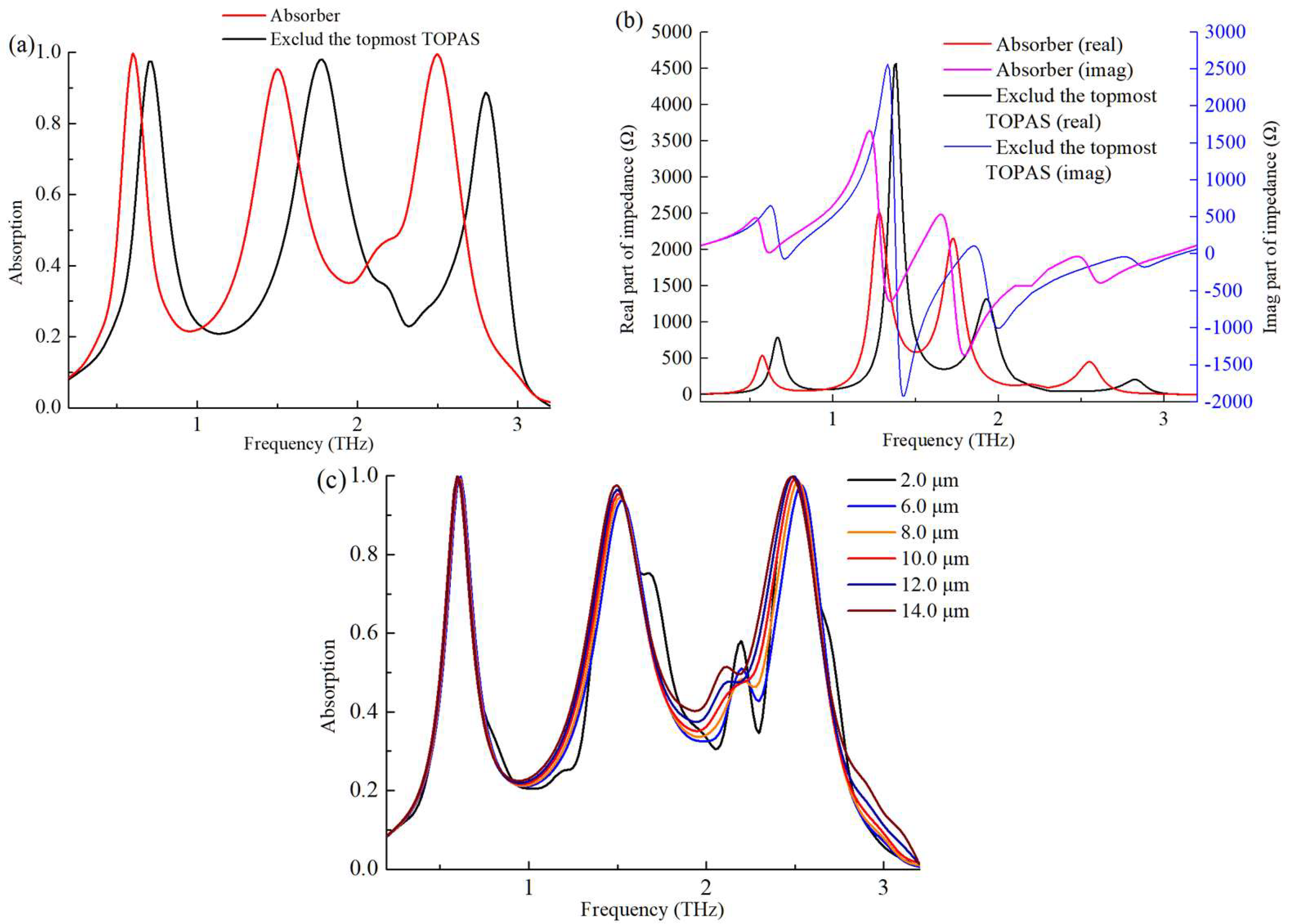
In the design of the absorber, an additional layer of dielectric was added to the top layer. Because 2D materials were stacked together by van der Waals forces between layers, the topmost TOPAS reinforced the stack of 2D materials and protected them from oxidation by moisture, air, etc. It can be seen from
Figure 9a, that the increase of the topmost dielectric changed the vertical electrical length of the space, and the peak of the absorption moved to the lower frequency. The topmost dielectric changed the impedance matching of the absorber (
Figure 9b). It had a relatively large influence on the imaginary impedance of the absorber at 1.5 THz. Additionally, at 2.5 THz, it had a greater impact on the real part of the impedance of the absorber. When changing the thickness of the topmost dielectric layer (2~14 μm) (
Figure 9c), the absorption of 0.6 THz remained essentially unchanged. As the thickness increased, the absorption increased slightly, and the frequency was gradually red-shifted. At the same time, between the two frequencies, around 2 THz, the absorption also started to gradually increase. Therefore, we can fine-tune the peak absorption frequency in a small range by changing the thickness of topmost TOPAS.
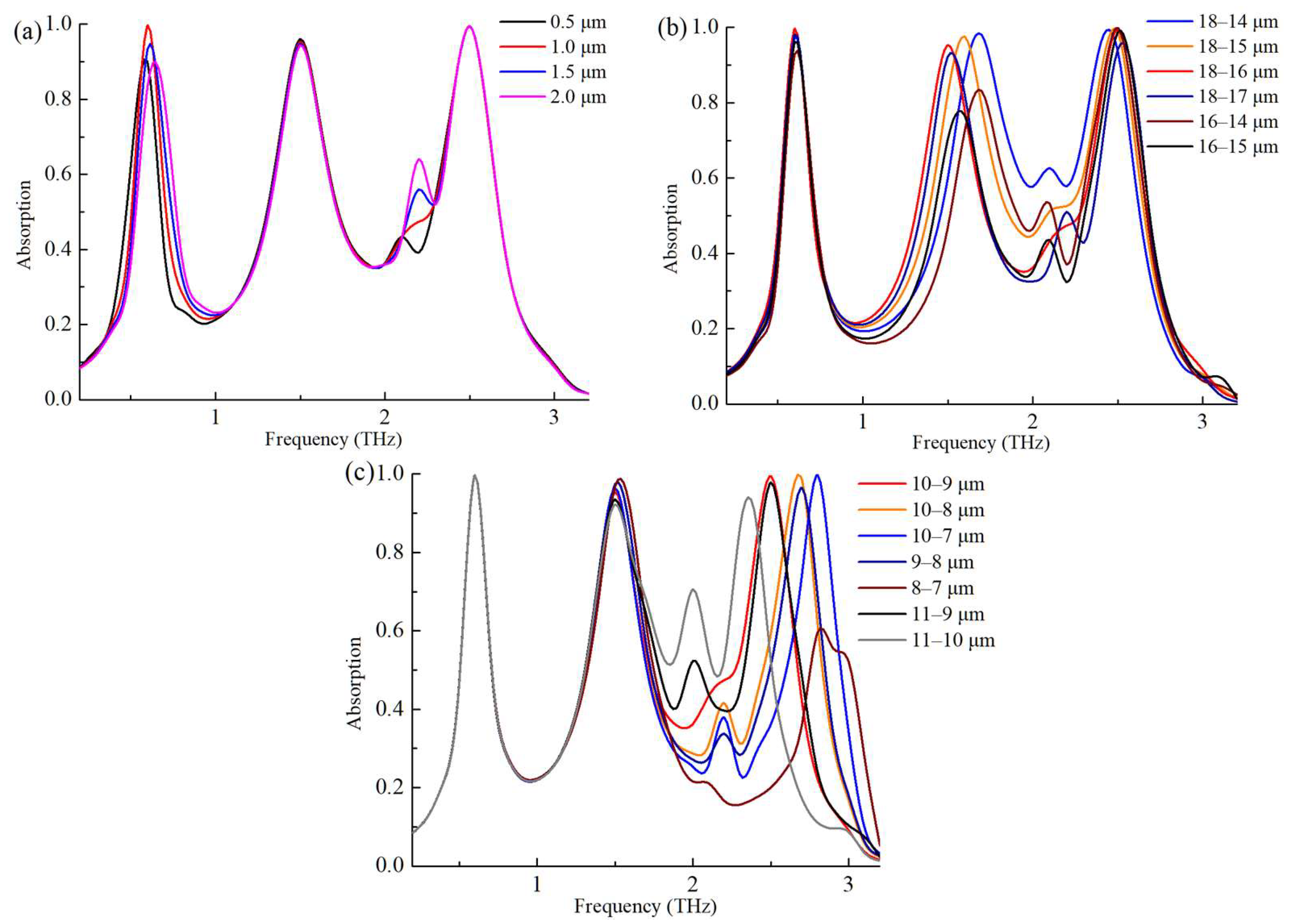
After the analysis of the 2D material layers and the topmost dielectric structure, the effect of each pattern part on the performance of the absorbers was investigated by varying the dimensions of the 2D material pattern (
Figure 10). Firstly, the width of the crossed linear slot was changed. From the previous analysis, crossed linear slots mainly affected the absorption of the 0.6 THz absorber. When the width of the crossed linear slot was varied from 0.5 μm to 2 μm, the absorption of the 0.6 THz absorber reached its maximum at 1 μm. Additionally, as the width changed, there was a small effect at 1.5 THz and 2.5 THz. It was consistent with the results of the previous electric field distribution diagram. When the size of the outer circular slot at the four corners was changed, the greatest effect was on the absorption at 1.5 THz. As can be seen from the curves at 1.5 THz, the frequency of absorption was blue-shifted as the width of the outer circular slot increased (18–16 μm, 18–15 μm, 18–14 μm). The inner diameter of the outer circular slot determined the frequency of the absorption. For example, 18–15 μm had the same absorption frequency as 16–15 μm, and 18–14 μm had the same absorption frequency as 16–14 μm. The size of the outer circular slot had little effect on the third absorption at 2.5 THz. The absorption at 2.5 THz was mainly affected by the size of the inner circular slot, as shown in
Figure 10c. Similar to the effect of the outer circular slot, the absorption was blue-shifted as the inner circular slot width increased (10–9 μm, 10–8 μm, 10–7 μm). The same inner diameter in the inner circular slot had the same absorption frequency (10–9 μm vs. 11–9 μm, 10–8 μm vs. 9–8 μm, 8–7 μm vs. 10–7 μm). Both the outer and inner circular slot dimensions had significant effects on the frequency band between two absorption frequencies.
From Equations (2) and (3), it can be seen that the carrier concentration (
n) and the chemical potential (
EF) were the parameters that affected the absorption characteristics of MoS
2 and graphene, respectively. In the current 2D material preparation process, parameters such as the carrier concentration of MoS
2 and the chemical potential of graphene could be changed by chemical doping, electrostatic doping, and other methods. When the carrier concentration of MoS
2 increased from 2 × 10
18 m
−2 to 12 × 10
18 m
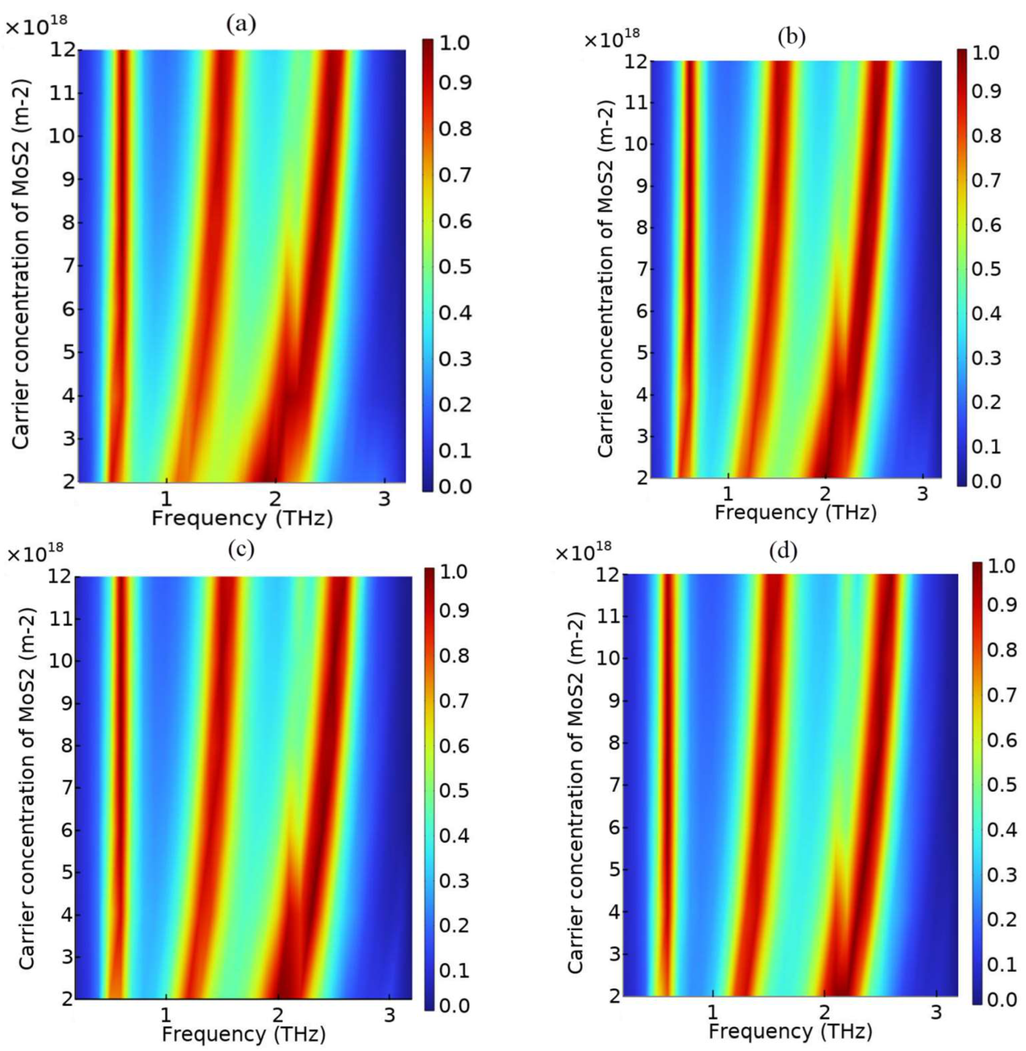
−2, the variation of the absorption was studied for the chemical potential of graphene (
EF) at 0.5 ev, 0.7 ev, 0.9 ev and 1.2 ev. In many studies involving multi-band absorbers of monolayer 2D materials, adjusting the carrier concentration of MoS
2 or the chemical potential of graphene had a significant effect on each absorbing peak in the absorber. This situation was significantly different from that shown in
Figure 11. In
Figure 11, as the carrier concentration of MoS
2 increased, the absorption at high frequencies was blue-shifted, that is, it moved to a higher frequency. Among the three frequencies, the highest frequency (2.5 THz) had the most obvious change, followed by the middle frequency (1.5 THz), and the absorption of the low frequency (0.6 THz) basically remained unchanged. From the comparison of
Figure 11a–d, it can be found that the smaller the chemical potential of graphene, the larger the absorption-frequency-shifted range. Compared with absorbers using only one 2D material, the stack of two 2D materials could simultaneously adjust more material parameters, increasing the degree of freedom. In the preparation of the absorber, the absorption frequency was changed by changing the doping characteristics of MoS
2 and graphene, thus making the absorber tuneable in a wider range.
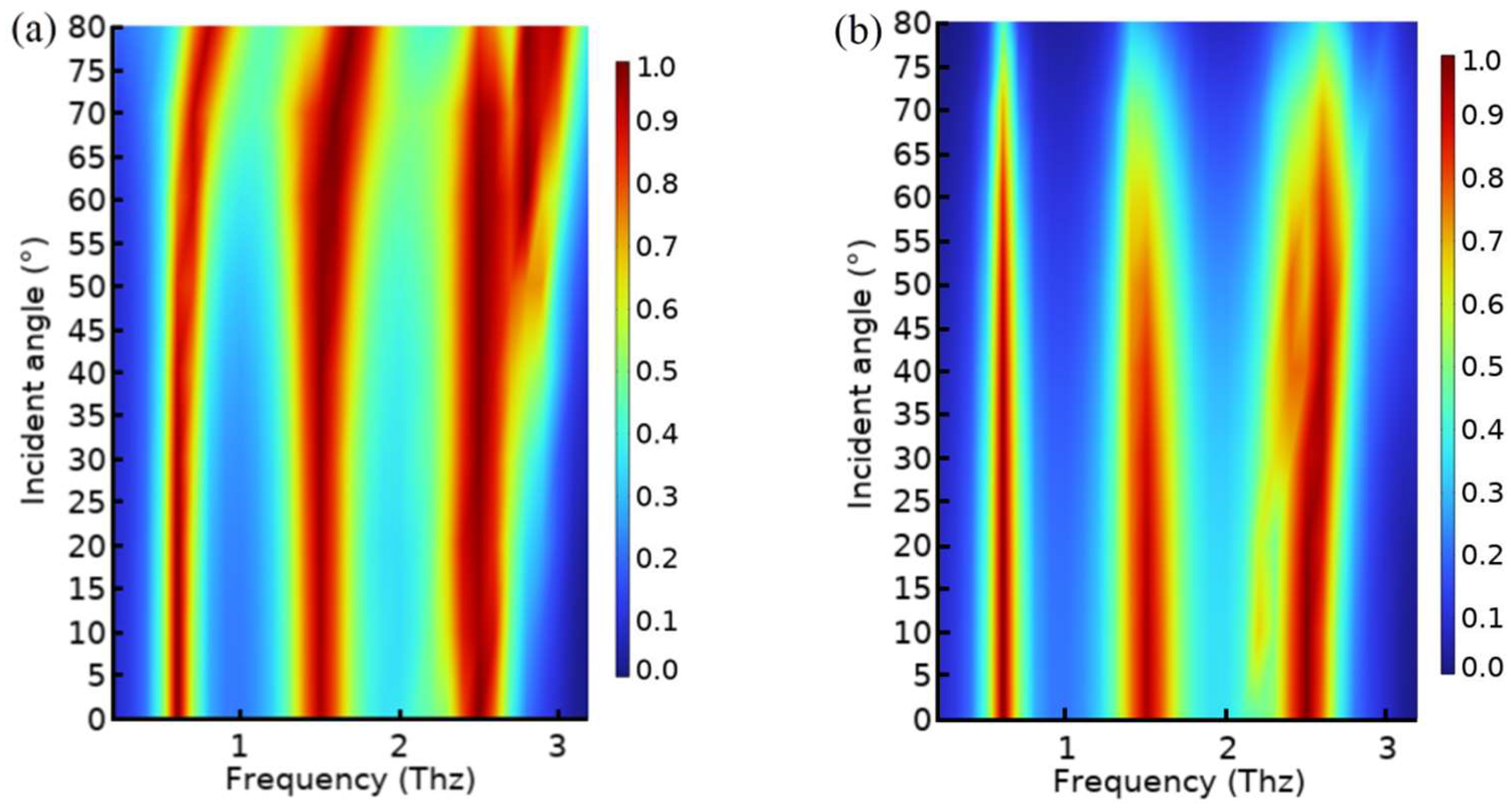
The above analysis analysed the characteristics of the absorber under the 0° incident angle electromagnetic wave in TM mode. Since TM mode and TE mode differ in their electromagnetic wave transmission, the effects of different incidence angles on absorption in TE and TM modes were investigated separately. In TM mode (
Figure 12a), 0.6 THz can maintain high absorption in the range of incident angles from 0° to 45°. Both 1.5 THz and 2.5 Hz had better absorption characteristics in the incidence angle range of 0° to 70°. Additionally, in TE mode, the incident angle range of 0.6 THz was better than 1.5 THz and 2.5 THz. The absorption of two high-frequency points was greatly affected by the angular variation.
After comparing the effects of incidence angle in different modes, the effects of different polarisation angles on the absorber’s performance were also compared. It can be seen in
Figure 13, that the absorber performance did not change in the range of 0° to 90° for the polarisation angle in both modes.
