Article

Solar Cell Detection and Position, Attitude Determination by Differential Absorption Imaging in Optical Wireless Power Transmission

Laboratory for Future Interdisciplinary Research of Science and Technology (FIRST), Institute of Innovative Research (IIR), Tokyo Institute of Technology, R2-39, 4259 Nagatsuta, Midori-ku, Yokohama 226-8503, Japan
*
Author to whom correspondence should be addressed.
Photonics 2023, 10(5), 553; https://doi.org/10.3390/photonics10050553
Submission received: 17 March 2023 / Revised: 12 April 2023 / Accepted: 29 April 2023 / Published: 10 May 2023

Abstract

:
In optical wireless power transmission, position, size, and attitude of photovoltaic device (PV) must be determined from light source. A method proposed in the previous report is based on selective absorption characteristics of PV, and it is detected by differentiating images of strongly absorbable wavelength and one not. In this study, using two infrared wavelengths, two kinds of targets were detected by differential absorption imaging. One was a GaAs substrate which simulates diffuse rear surface, and the other was a real GaAs PV. It was found that the substrate’s reflective characteristic was diffuse, and the solar cell’s was mainly non-diffuse and accompanied by small diffuse component supporting wide-angle reflection. Using this feature, the position of the GaAs solar cell could be determined within a wide range of angle. Its attitude could also be determined with an accuracy of ±10 degrees to its normal. The position of diffuse GaAs substrate could be determined within a wide range of angles, and its attitude determination was proposed by exploiting its varying apparent size with tilt angle. Broad reflection characteristics of the GaAs substrate enabled attitude determination for a wide-angle range, and determination around normal would be erroneous.

1. Introduction

In the coming wireless society [1], Optical Wireless Power Transmission (OWPT) is expected to play an important role [2,3,4]. Since it irradiates light beam to photovoltaic device (PV) from light source, it has advantage of transmitting power to a long-distance target [5,6,7,8]. To increase power generation efficiency to irradiated power, sophisticated beam alignment and shaping combined with some relaxation strategy [9,10] is necessary. Moreover, PV’s position, size, and attitude must be accurately determined from the light source. Therefore, detecting solar cells’ position and attitude are essential building blocks of the operational OWPT system. However, studies regarding them are not so many so far. In former researches, PV detection are studied by means of image processing of its outline or specific markers [11,12]. It is reported that detection became unstable in case of varying background illumination by weather or time [11].
Thus, robust detection of PV is one of critical technical challenges in OWPT. In the method proposed previously, robustness is achieved by utilizing intrinsically built-in feature of PV. PV is detected by differentiating images of wavelength which is strongly absorbed by it (hereafter λ O N ) and one which is not (hereafter λ O F F ). During this differentiation, the unnecessary background is subtracted. Differential technique is widely used in many technical areas both in signal and image processing [13,14,15]. This technique was applied to solar cell detection in OWPT [16]. A proof-of-concept study was conducted utilizing λ = 532 nm and Si substrate as a target. In this study, following the previous one, detection and determination of position, area and attitude of GaAs substrate and real GaAs PV were investigated utilizing two infrared wavelengths 850 nm ( λ O N ), and 940 nm ( λ O F F ).
Two options would be expected for rear surface treatment of solar cells. One is diffuse, and the other is non-diffuse. Angle dependence of detection were analyzed for both options and attitude determination were proposed. GaAs substrate showed broad diffuse reflection characteristic. On the other hand, PV showed sharp angular dependence of reflection. The existence of solar cells could be detected within a wide angle range for both targets. Regarding attitude detection, normality of PV could be detected within ±10 degrees. For a diffuse GaAs substrate, attitude determination based on apparent width of the target was investigated and experimentally validated.
The structure of this paper is as follows. Detection experiments of GaAs substrate, including determining its center coordinates and area, are reported in Section 2. The ‘threshold equation’ is derived in Section 3, which connects signal electron number and minimum grayscale level of differential absorption image at the threshold. In Section 4, real thin-film GaAs solar cell detection experiments are reported. Angular characteristics of GaAs substrate and solar cell detection are reported and discussed in Section 4 and Section 5. Finally, in Section 6, the outcomes of this study are summarized.

2. GaAs Target Detection by Means of Infrared Differential Imaging

2.1. Configuration of Experimental Apparatus

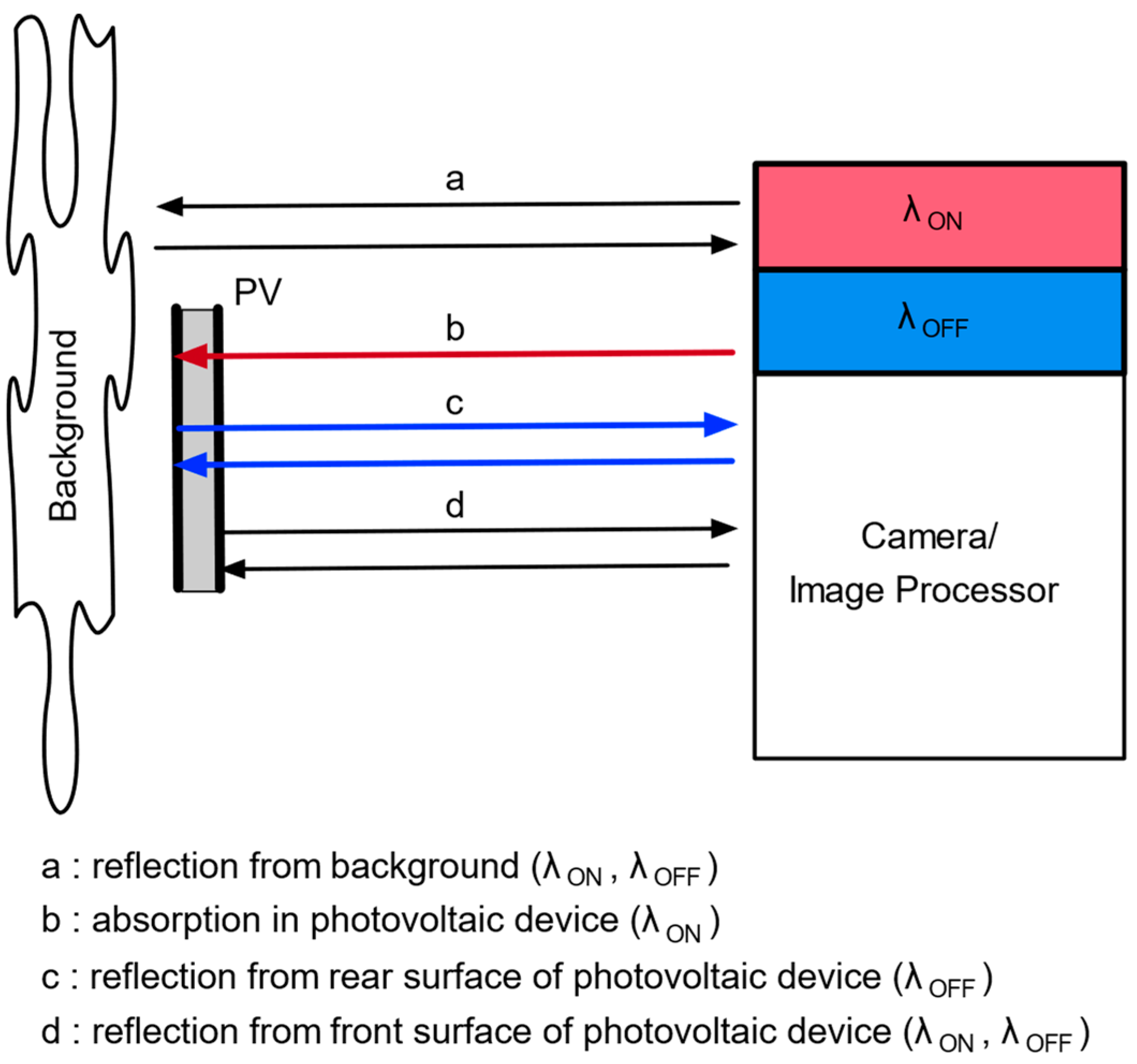
PV detection by differential absorption imaging utilizes selective absorption characteristics of PV between two different wavelengths. The principle of solar cell detection by differential imaging is described in Figure 1 and [16] in detail.
In the previous study, experiments were conducted with λ = 532 nm, and differential images were generated from Si substrate and frost glass images [16]. Then, determination of X and Y center coordinates, and area of the Si substrate were discussed, including their accuracies. In this study, similar experiments were conducted using more realistic targets. In many PV, semiconductors such as Si or GaAs are utilized, and differential absorption imaging takes advantage of the wavelength dependence of absorption of semiconductors. Absorbable wavelength λ O N should be set below and non-absorbable wavelength λ O F F should be above the bandgap wavelength of semiconductors. Two wavelengths should be close enough so that the two wavelengths experience almost the same background, and the image-capturing camera in Figure 1 should have sensitivity for both wavelengths. In the experiments in this study, the Si sensor camera was exploited like in the previous one, GaAs was chosen as the target material, and λ O N , λ O F F were selected as 850 nm and 940 nm, respectively.
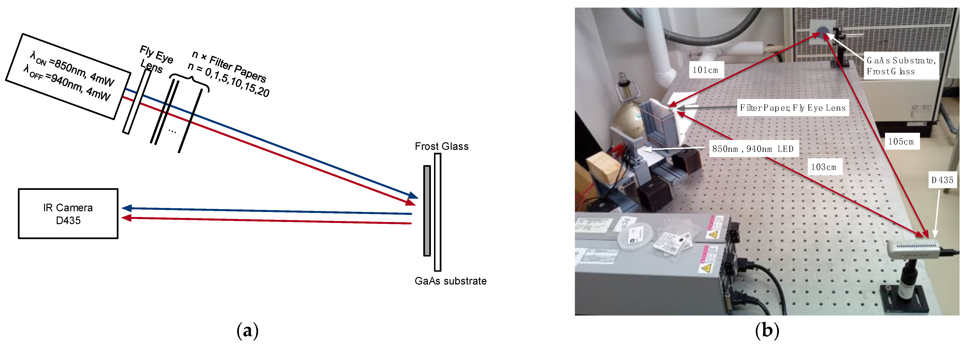
Figure 2 shows configuration and layout of this experiment. The transmitter assembly consists of series-connected two LEDs for both 850 nm and 940 nm. Emitting power of individual LED is calculated as 2 mW from the data sheets [17,18]. For the infrared camera, Intel D435TM [19] depth camera was used, and one of its two infrared output streams (left channel) was inputted to the image processor (PC). As for software running on the image processor, D435 SDK [20], Python [21] and Open CV [22] were used to control the camera. Irradiated power onto the target is controlled by changing the number of filter papers, which has scattering and reflection characteristics, in front of the fly eye lens in Figure 2a. In this paper, such ‘power control status’ is denoted as P0, P1, etc. P0 means that fly eye lens with no filter paper, and P1 means that fly eye lens and 1 (one) filter paper, etc.
Regarding parameters setting of D435, gain was set to 240, and image size of raw data was set to 640 × 480 px throughout this study. Other internal parameters were not changed from their default values.
Images were captured by varying exposure times as 25, 50, 100, 250, 500, 1000, 2500, 5000, 10,000, 25,000, 50,000, 100,000, 200,000 μs, and power control status as P0, P1, P5, P10, P15. Captured 640 × 480 px images were trimmed down to 34 × 33, 51 × 49, 68 × 66, 102 × 99, 170 × 165, 238 × 231, 324 × 330, 324 × 480, 640 × 480 px (non-trimmed). Differential and binarized images were generated for all combinations of the parameter sets, and GaAs substrate images were extracted from the binarized images. For image processing of the captured images, MathematicaTM [23] was used.

2.2. GaAs Substrate Detection by Means of Infrared Imaging

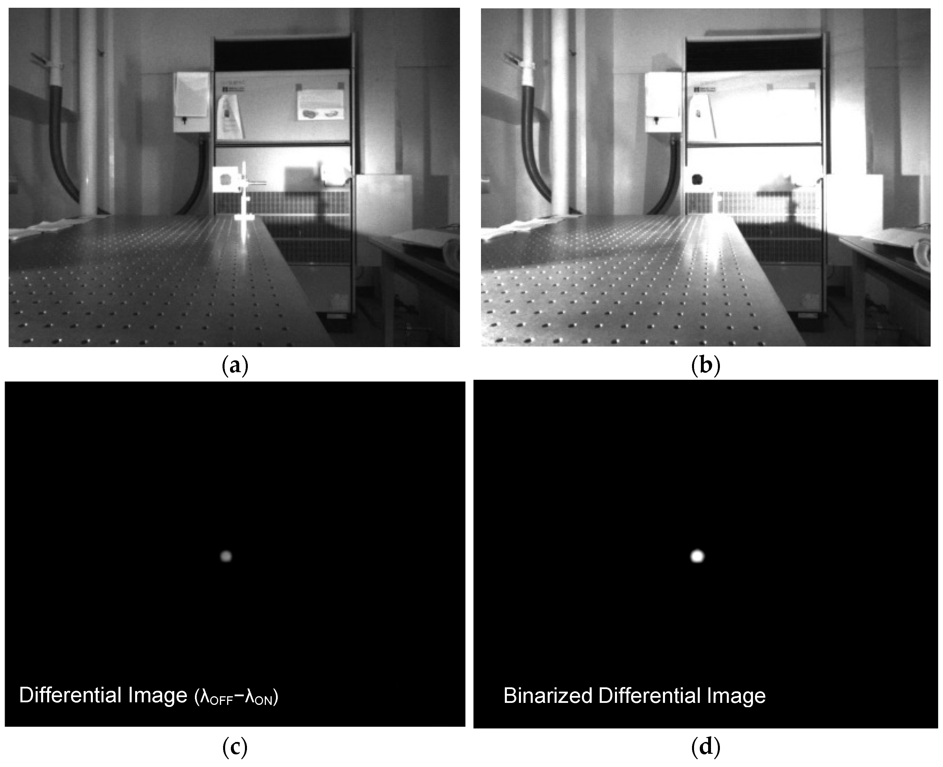
Infrared GaAs images captured by the measurement system are shown in Figure 3 (Exposure time 200,000 μs, P0).
Comparing λ O F F image (Figure 3a) with that of λ O N (Figure 3b), the latter is brighter than the former due to the wavelength dependence of the camera’s sensitivity. Instead of applying brightness correction, the grayscale level of each pixel in the differential image ( g s d i f f ) is calculated by Equation (1), which can be referred to as ‘over subtraction’. This formula does not affect the target region in which λ O F F image is expected to be brighter than λ O N . On the other hand, it eliminates unnecessary background in which λ O N image is expected to be brighter than λ O F F .
g s d i f f = g s O F F g s O N , g s O F F g s O N 0 , g s O F F < g s O N
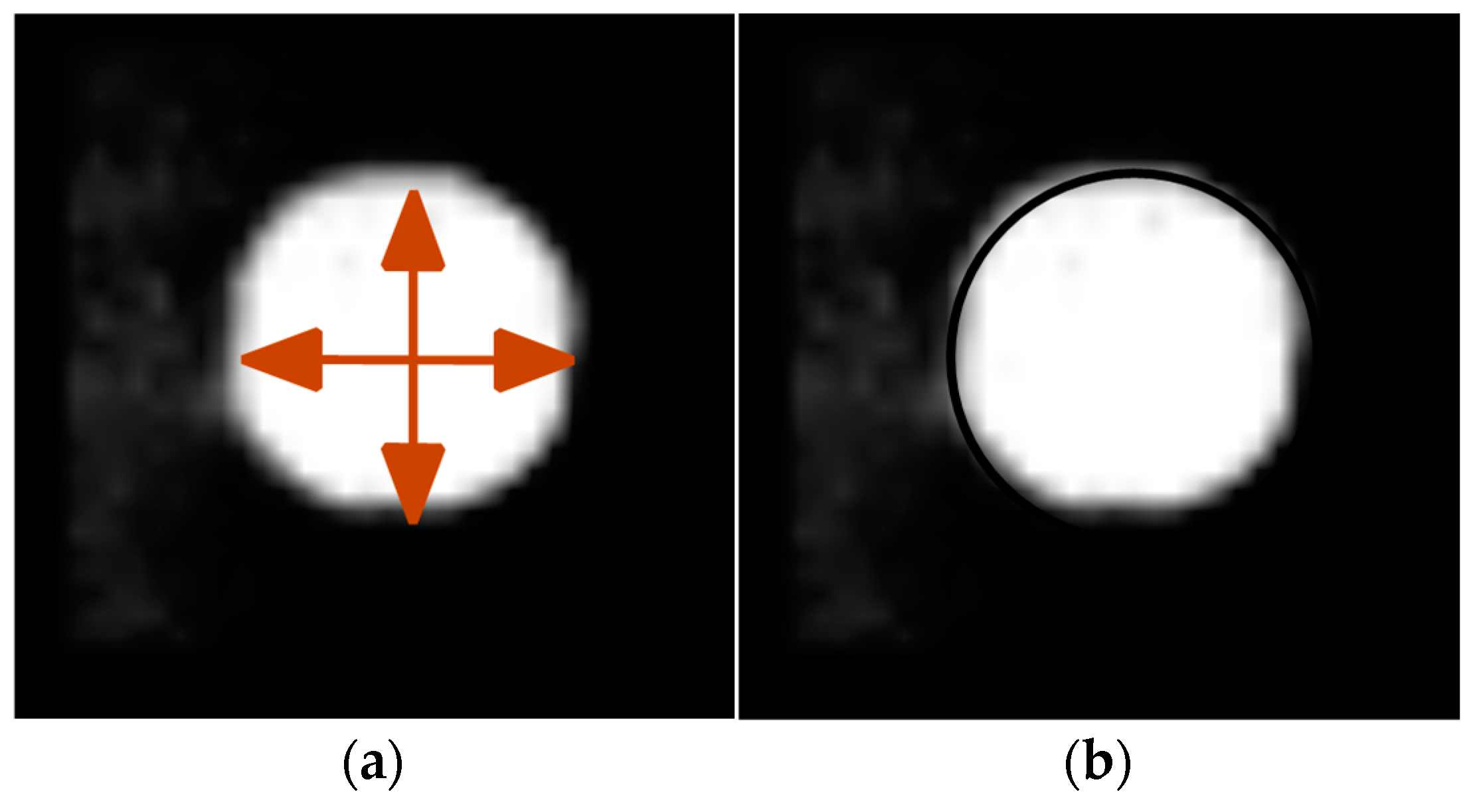
The threshold of binarization is determined by Otsu algorithm [24] like in [16]. Specification of target GaAs substrate is that manufacturer AXT Inc. Fremont, CA, USA [25], n-type, carrier concentration 2 ~ 3 × 10 18   c m 3 , diameter 2”, thickness 350   μ m , surface orientation (001). Detection of the target by differentiation and binarization is demonstrated in Appendix A. The center coordinates and the area, as shown in Figure 4, are estimated from each detected GaAs image.
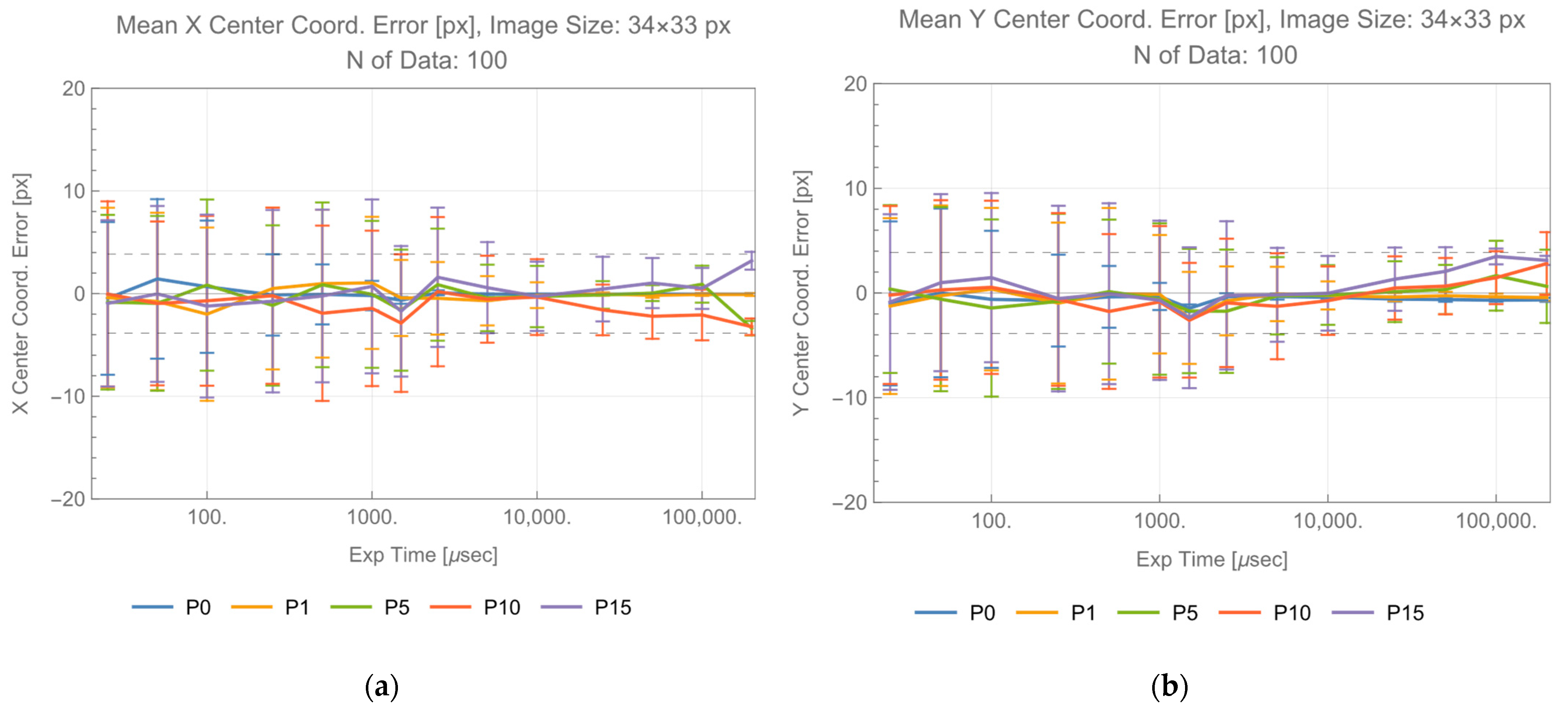
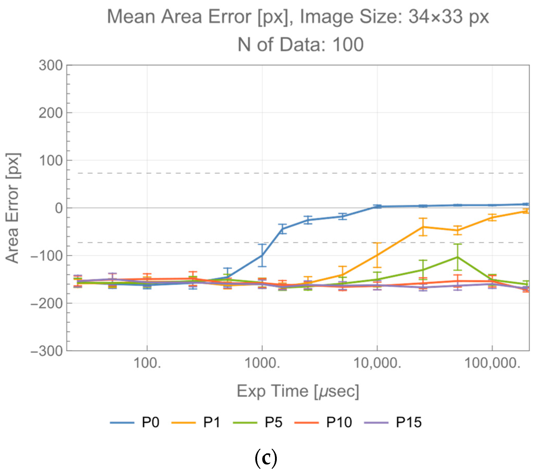
Figure 5 is an excerpt from data reduction products, whose image size is 34 × 33 px. After estimating the center coordinates and the area from each image, their mean values with 1 (one) σ error is plotted in the figure. System requirements for the center coordinates and the area can be calculated by the method described in [16]. Assume OWPT is a cooperative configuration in which the transmitter and receiver cooperate to align their attitude with each other. The irradiated beam size is 50 % of the receiver size at its entrance, as in the case of utilizing a fly-eye lens module [7,26,27]. The requirement for misalignment is determined by power generation ratio calculation [7].
Assuming the power generation ratio = 80% is the limiting case, the requirement for the center coordinate is given by 0.718 × G a A s   r a d i u s / 2 . The radius of the GaAs substrate was directly read from the captured images, and its mean value was 7.6 px. The requirement for the center coordinates is 3.86 px. The requirement for the area is ±0.4 S, where S is the area of the substrate. The mean value of the substrate area was 181.94 px. The requirement for the area becomes ±72.78 px. These requirements are included in Figure 5 as horizontal dashed lines. It can be seen from Figure 5 that requirements are accommodated, and the target is detectable.

3. Comparison of GaAs Substrate Detection by Infrared Imaging with Si Substrate Detection by Visible Light Detection

From the data in Figure 5, both X, and Y center coordinates are within the requirements limit for every exposure time of P0 and P1. The areas are within them for exposure time longer than 1000 μs for P0, and 15,000 μs for P1. Data using visible light are included in [16]. Comparing these threshold exposure time of detectability, ratio of infrared to visible is constant regardless of power control status, as shown in Table 1.
The number of signal electrons generated in image capturing camera is calculated as Equation (2) proposed in [16],
N s = λ / h c η r η t η Q P t F R ρ A r E x p / π R 2
where η Q : quantum efficiency of the camera sensor, η r : efficiency of camera optics, ρ : diffuse reflectivity of the target, h c / λ : photon energy of the incident beam, E x p : e x p o s u r e t i m e , P t : incident beam power, A t r : area of irradiated beam at the target point, η t : efficiency of transmitter optics (including intensity reduction due to fly eye lens and filter papers), R : distance to the target, A S C : Area of the target, and F R is defined in Equation (3).
F R 1 f o r   A S C A T R A S C / A t r f o r   A S C < A t r
The ratio of the threshold exposure time of visible to the one of infrared is evaluated using Equation (2). Regarding signal electron number of infrared, one for λ = 940 nm is necessary for evaluation. The parameters, F R , η r , η t , A t r , A r , R can be regarded as same between the two experiments. The other parameters are distinguished by adding subscripts ‘532’ for parameters included in λ = 532 nm experiment and ‘940’ for λ = 940 nm. Then,
N s 532 N s 940 = 532 η Q 532 P t 532 ρ 532 E x p 532 940 η Q 940 P t 940 ρ 940 E x p 940
Each parameter is evaluated as follows.
  • Exposure time
From the data of the two experiments,
E x p 532 E x p 940 = 12 ~ 13
2.
Quantum efficiency
Since the quantum efficiency data of the Si sensor inside D435 is not disclosed, this parameter should be evaluated by other available CMOS sensor data. Several commercial CMOS sensor data are compiled in the datasheets [28]. The ratio of quantum efficiency of CMOS sensor at λ = 532 nm to λ = 940 nm looks roughly varying from 4:1 to 10:1, and
η Q 532 η Q 940 = 7
is adopted as the mean value.
3.
Power
Since λ = 532 nm experiments, its power was 5 mW [16], power can be evaluated as
N s 532 N s 940 = 5   m W 4   m W = 1.25
4.
Diffuse reflectivity
It is evaluated as
ρ 532 ρ 940 = 1.7 ~ 2.75
Details are described in Appendix B.
From the series of evaluations above,
N s 532 N s 940 = 0.65 ~ 1.13
Since this ratio is close to 1 (one), the threshold number of electrons for GaAs and Si substrate detection would be conjectured as constant regardless of wavelength ( N s t h r e s h o l d N s 532 = N s 940 ) . On the other hand, N s t h r e s h o l d would be proportional to the grayscale threshold level, identified as the binarization threshold.
Differential intensity ( I d i f f ) is defined as follows.
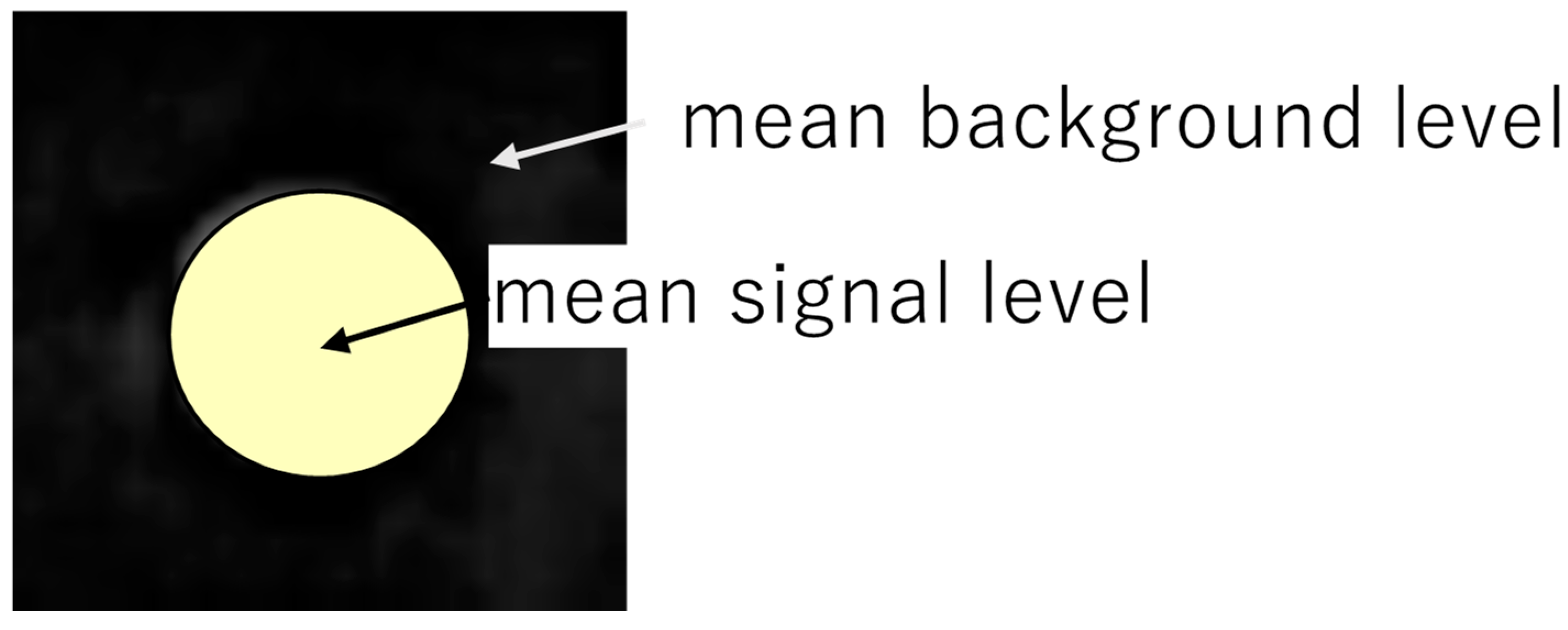
I d i f f = I T G T I B G
where I T G T is mean level inside the target region in Figure 6, and I B G is mean background level. As a result, I d i f f is mean signal level inside the target region.
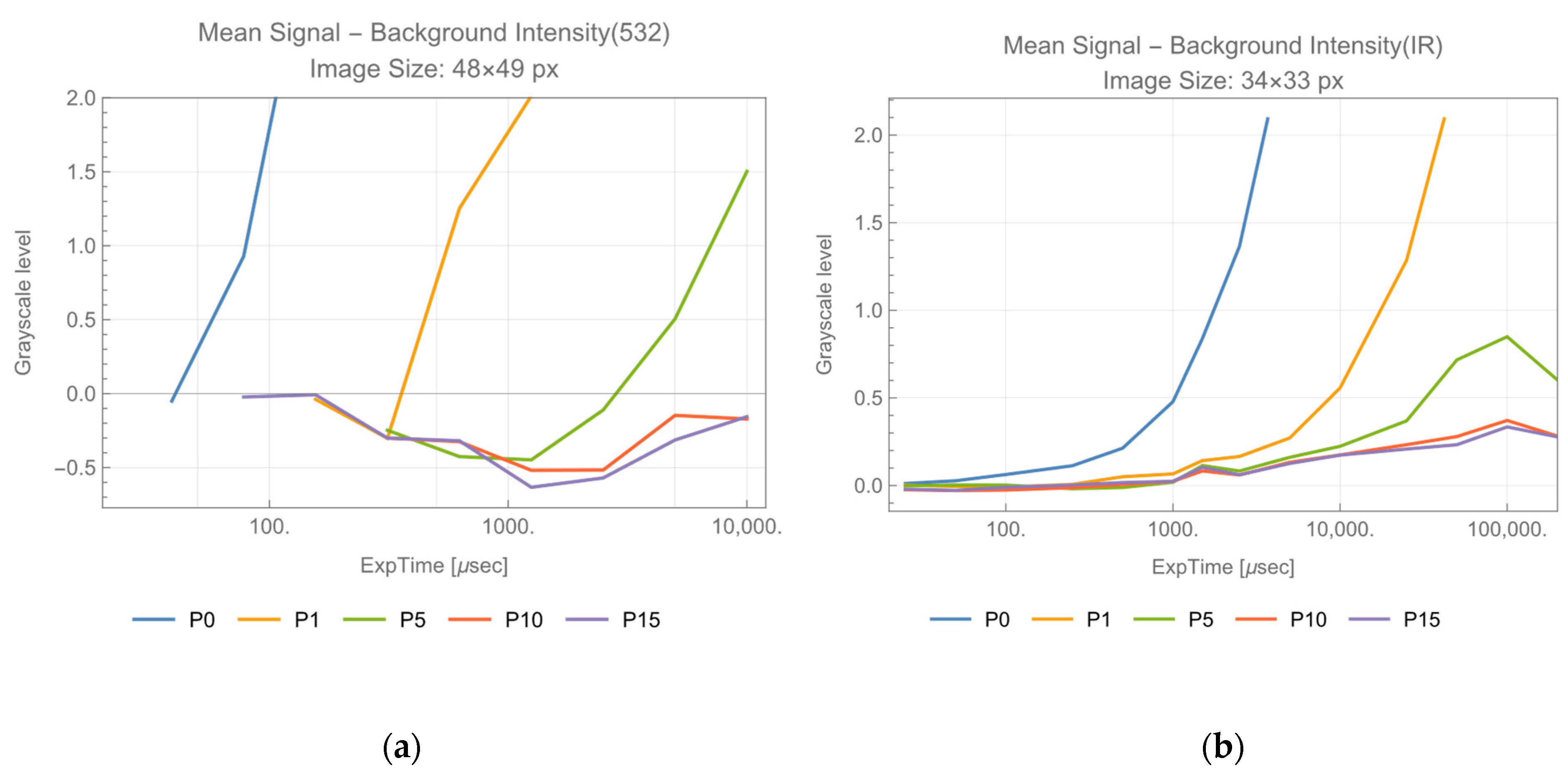
Considering sensor output is 8-bit grayscale, I d i f f is normalized by 1/255, which is the minimum resolution of 8-bit. Figure 7 shows the normalized I d i f f plot against exposure time.
These plots show that threshold exposure time of both visible and infrared experiments correspond to the unit value 1 (one) in the longitudinal axis. The above discussions show that threshold signal electron number and threshold differential intensity are constants between the two experiments. This suggests that the following ‘threshold equation’ holds at the threshold of target detection regardless of wavelength used in the two differential absorption imaging experiments.
K λ / h c η r η t η Q P t F R ρ A r E x p / π R 2 t h r e s h o l d = Δ I d i f f
Here, Δ I d i f f represents threshold differential intensity which is identified as binarization threshold and whose minimum value is 1 (one) bit of grayscale level (1/255 for 8 bit), and K represents coefficient to transform signal electron number to a grayscale level which also depends on configuration of measurement system. All parameters on the left-hand side of Equation (11) are for λ O F F . The generalized form of the equation is obtained by including a term for λ O N which is negligible in these experiments.
K λ / h c η r η t η Q P t ρ A r λ O F F K λ / h c η r η t η Q P t ρ A r λ O N F R E x p / π R 2 t h r e s h o l d = Δ I d i f f
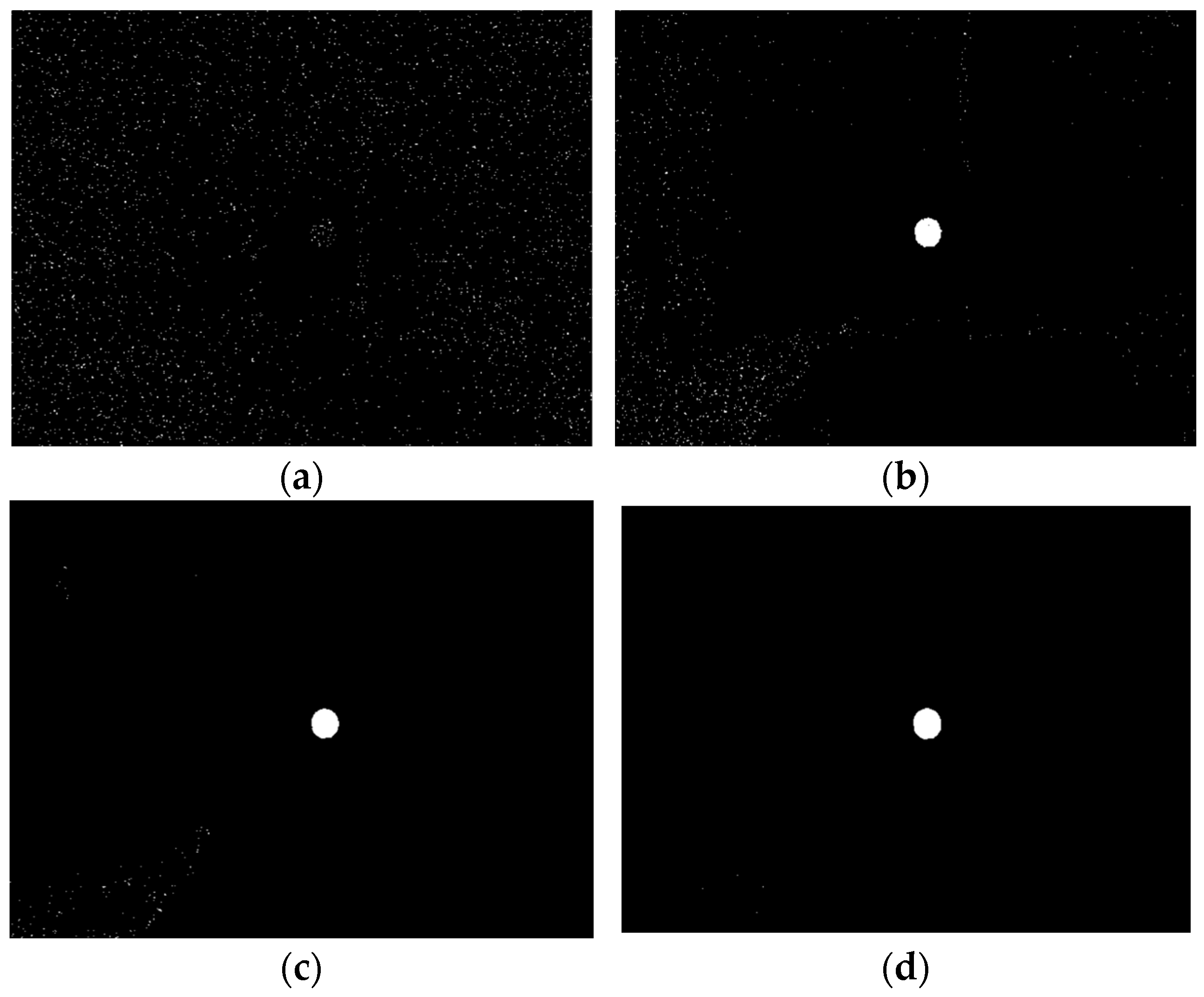
The first term of Equation (12) in the left-hand side parenthesis represents the parameters for λ O F F and the second one represents λ O N . A set of parameters on the left-hand side of Equation (11) or (12) determines the threshold differential intensity (maximally settable binarization threshold) on the right-hand side. The right-hand side of the threshold requires the necessary parameters in the left-hand side to support the binarization threshold to be set. It should be noted that Equations (11) and (12) are defined by mean noise value in a certain region and noise is generated randomly within such regions. Consider that noise covers uniformly over the entire image of λ O F F and λ O N .This case would occur with a long exposure time. Differentiating λ O F F and λ O N images by Equation (1) would cause noise reduction in the resultant differential image. This is observed in Figure 8. It shows images of various exposure time with constant binarizing threshold of 1/255. It is seen that increments of exposure time cause noise reduction. In Figure 8a, whose exposure time is 500 μs, a tiny white dot of noise is spread over the entire image, and the GaAs image cannot be seen. As exposure time increases in Figure 8b,c, such noise decreases gradually, and the GaAs image appears at the center. Finally, in Figure 8d, only GaAs image can be seen. In this case, the second term of Equation (11) would be ignorable, and a globally clear noiseless image can be generated even for differential intensity Δ I d i f f = 1/255. Long exposure time causes noise reduction even for non-trimming images.
In case that noise would not cover the entire image, such noise would remain in some regions in the differential image after differentiation. This case would occur in a short exposure time. In such a case, there would be two strategies to avoid the noise effect. One is to increase Δ I d i f f from 1/255 to an appropriate value. This causes an impact on the system parameters on the left-hand side of Equation (12), such as an increment of irradiation power. The other option would be trimming images to an appropriate size in which the target size dominates the entire image. For example, in Figure 7, images were trimmed to 48 × 49 px for visible and 34 × 33 px for infrared. For short exposure time data in Figure 7, this trimming looks helpful to reduce noise and make Δ I d i f f minimum. However, the larger the size of the images, the noisier the resultant images become. This phenomenon was observed in the experiments in [16]. For longer exposure time data in Figure 7, both long exposure time and trimming effects would have cooperatively caused noise reduction in the resultant images.
Exposure time should be determined by system requirements, especially by its real-time requirement. It would be necessary to estimate the noise remaining in the differential images according to the determined exposure time and develop plans of Δ I d i f f setting. Equations (11) and (12) provide logic for such system design strategies.

4. GaAs Solar Cell Detection by Means of Infrared Differential Absorption Imaging and Its Attitude Determination

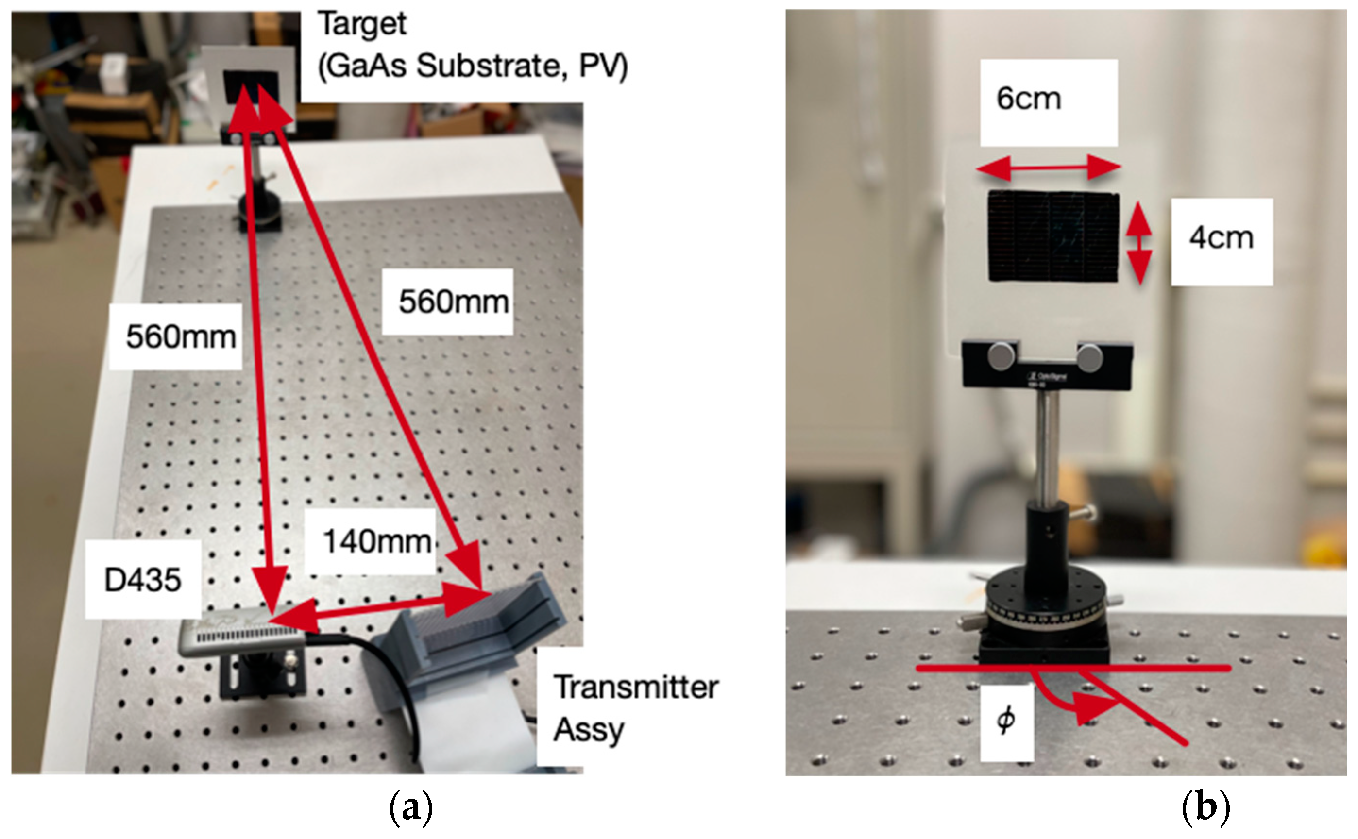
A real thin film GaAs solar cell detection experiments were conducted (Manufacturer Advanced Technology Institute, Tokyo, Japan [29], five cell series connected). The GaAs solar cell size is 6 cm × 4 cm. Its front surface is GaAs solar cell, and its rear surface is a copper electrode. The solar cell is fixed on a rotatable stage, and its rotation angle ϕ is set to 90 degrees when it faces normal to the camera.
During trial phase, strong non-diffuse reflection was observed near the solar cell normal and weak diffuse reflection from large angles. From exposure time point of view, a short exposure time would be enough to detect vital components near the normal, and a long one would be necessary to detect weak components in large angles. Considering the noise reduction effect described in the last section, large angle components are expected to be detected by setting long exposure time and global binarization threshold of Δ I d i f f = 1/255. Regarding the detection of strong components near the normal, there are two options. One is to increase the binarization threshold, since such reflection is due to high reflectivity in the left-hand side of Equation (12), Δ I d i f f can be increased accordingly. Another option is that Δ I d i f f is kept globally at its minimum 1/255. Since the solar cell detection algorithm in these experiments is that the connected component with the maximum area in the binarized image is regarded as the solar cell, the area of the connected solar cell image generated by strong reflection would become dominant even in the noisy image of short exposure time. In such a case, the solar cell image would be detected even with short exposure time and minimum Δ I d i f f . The second option looked simpler and was tried. Δ I d i f f was kept globally 1/255 for every exposure time, and the solar cell was successfully detected.
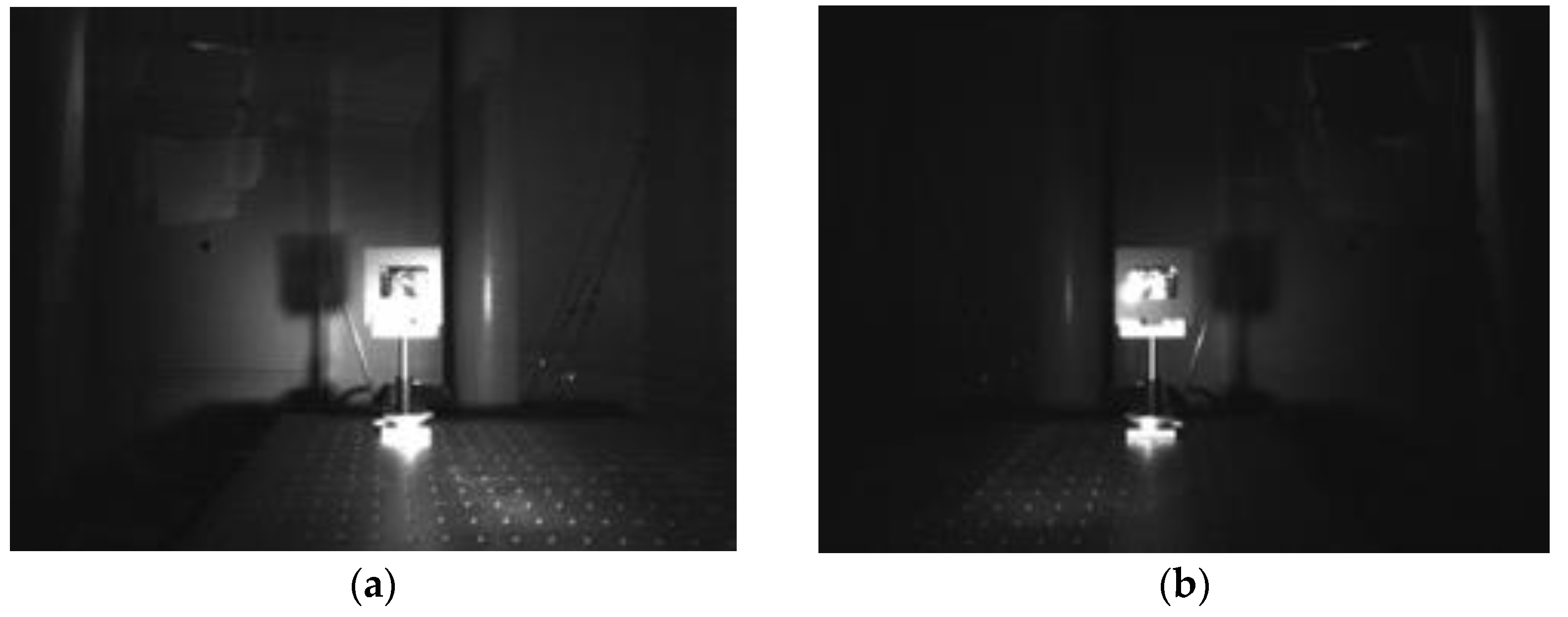
Experiments were conducted for various angles of the rotatable stage shown in Figure 9. They are 50, 60, 70, 75, 80, 85, 90, 95, 100, 105, 110, 115, 120, 130, and 140 degrees. An excerpt of λ O N image (a) and λ O F F (b) are shown in Figure 10 (Exposure time 25,000 μs, P0, ϕ = 95 degrees).
The solar cell was detected in two image sizes. One is 82 × 83 px, the same size as the background frost glass. The other is non-trimmed 640 × 480 px. The solar cell was detected successfully in both image sizes. Appendix C includes a data set of 82 × 83 px. The center coordinates, and the area was determined. An excerpt from the data reduction products is shown in Figure 11. In this case, 82 × 83 px images were used for determination.
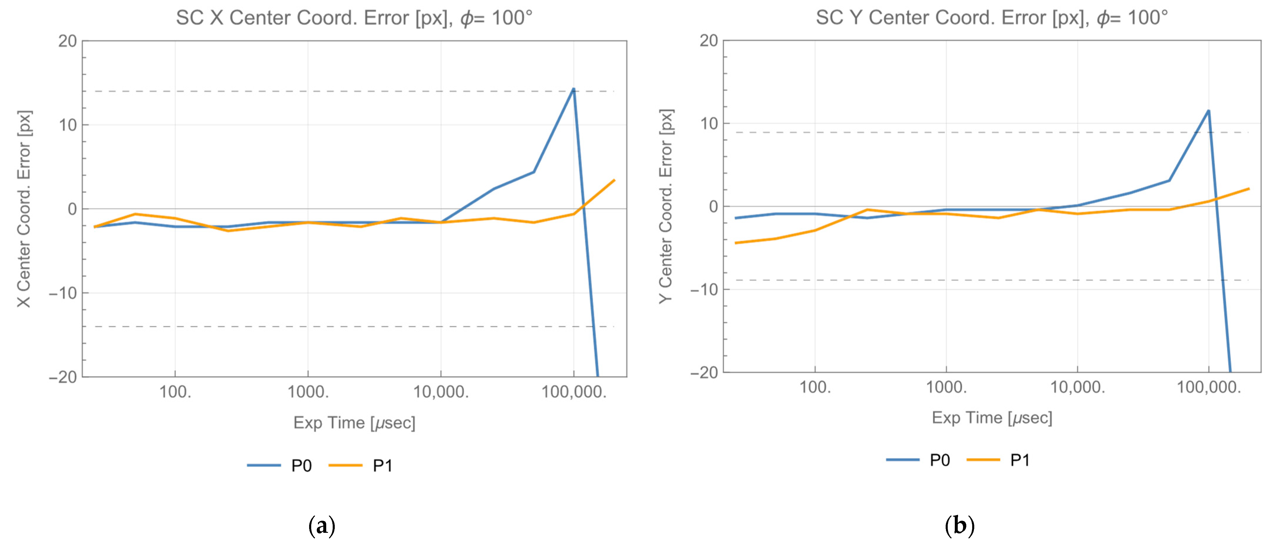
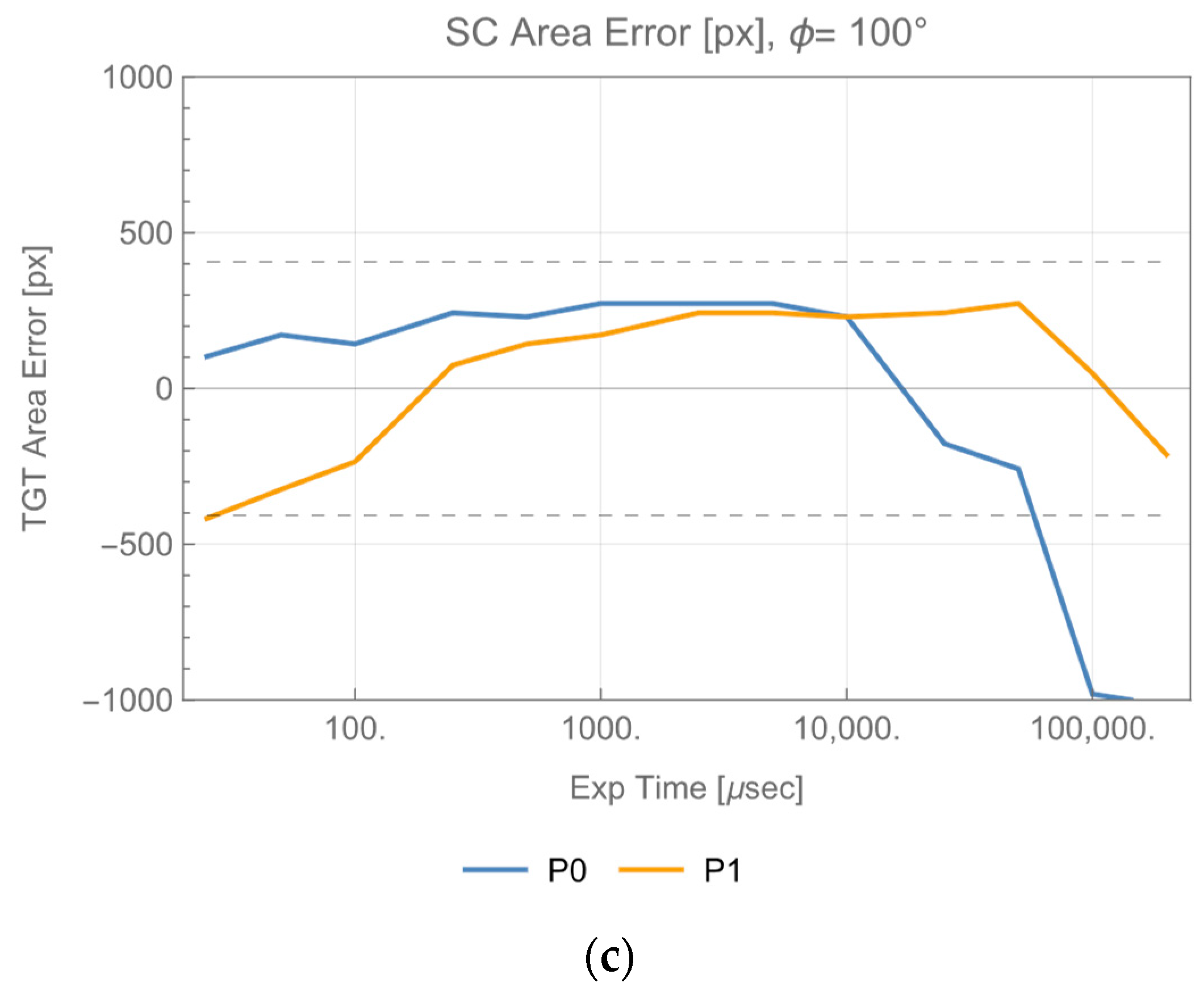
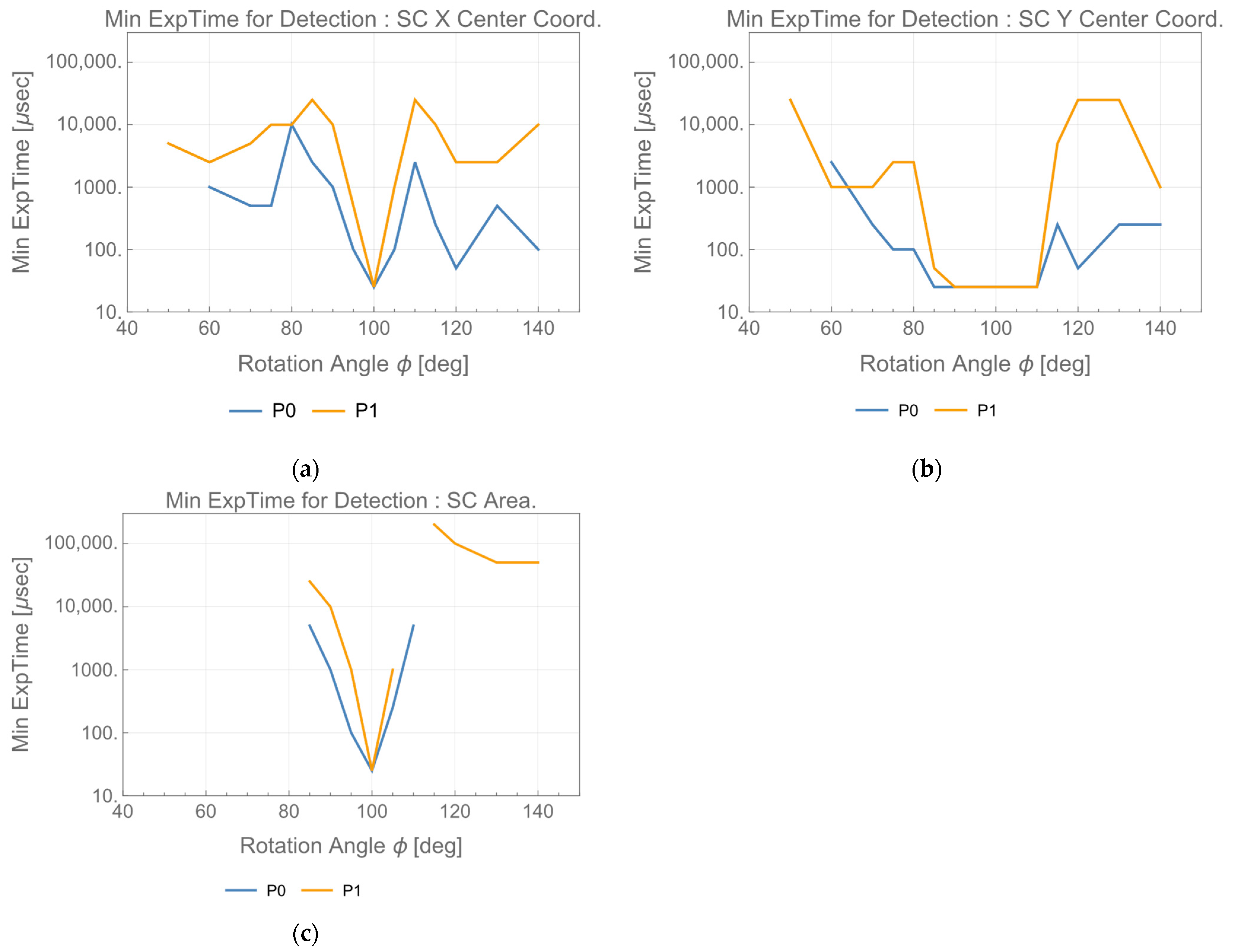
In Figure 11, the requirements shown as horizontal dashed lines were calculated like the GaAs substrate case. The values vary with the angle ϕ. In the case of ϕ = 100 degrees, the requirements for the X, Y center coordinates are 41.5 and 43.5 px, respectively, and the requirements for the area are 803.5 px. These requirements are different from the requirements plotted in Figure 5. This is because the experiment layout of Figure 9 for this solar cell detection differs from Figure 2 for the GaAs substrate. All the requirements are stably accommodated from exposure time = 25 μs. In case of prolonged exposure time, accommodation fails. This reflects the situation that both λ O N and λ O F F images are saturated, and solar cell images cannot be detected by differentiating the two images. Appropriate exposure time should be set to avoid such saturation. Generally, the minimum exposure time which accommodates the requirements depends on the rotation angle ϕ . Figure 12 shows the angular dependence of the minimum exposure time, accommodating the requirements.
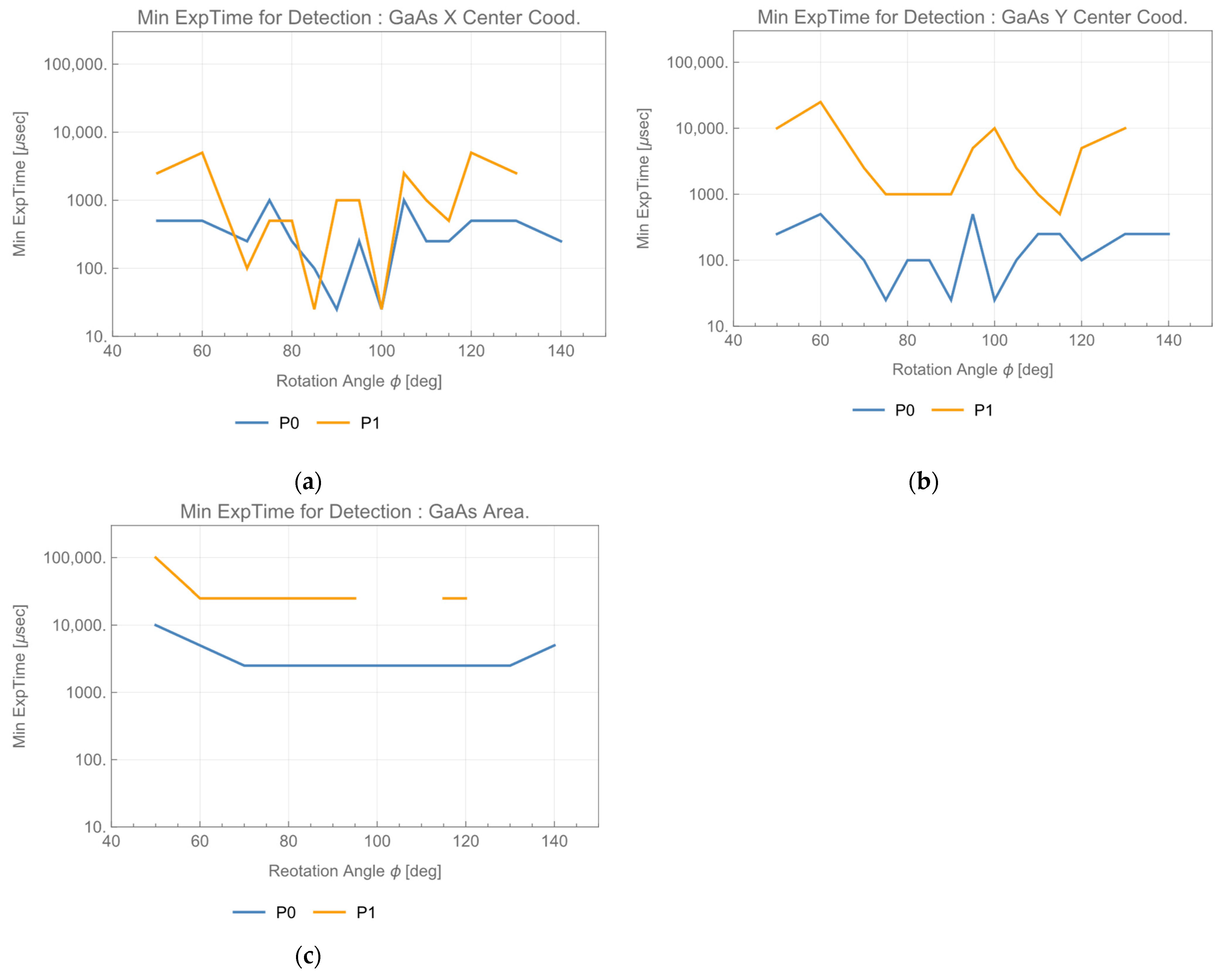
In addition to non-diffuse, rear surface treatment of solar cells has diffuse options. To investigate the attitude determination of this case, similar experiments were conducted using GaAs substrate. GaAs substrate could be stably detected within the range of 50~140 degrees. Like Figure 12, the angular dependence of minimum exposure time, which accommodates the requirements, is plotted in Figure 13. In the case of ϕ = 100 degrees, requirements are calculated as 43.1 and 46.4 px for X, and Y center coordinates, respectively and 1017.4 px for the area. Also, in this case, the binarization threshold was set to 1/255 regardless of image size.

5. Discussion

All the plots in Figure 12 have concave-shaped peaks around ϕ = 100 degrees. This shows that the rear surface of the GaAs solar cell has non-diffuse reflection characteristic. The peak angle corresponds to the angle that the incident beam is reflected to the camera. This can be calculated by using the dimensions in Figure 9a. Figure 12 shows that the X, Y coordinates can be determined within the range of ϕ = 50~140 degrees. On the other hand, the area determination is limited within the range of ±10 degrees around ϕ = 100 degrees. The fact that the weak large-angle reflection is detected means that small diffuse reflection component accompanies the main non-diffuse one. Exploiting this feature, determination of the solar cell normal would be feasible. Detectability criteria proposed in [16] require that the X, Y center coordinate and the area should simultaneously accommodate the system requirements. For the GaAs solar cell, these criteria are satisfied in the area near the normal of the solar cell. For a cooperative OWPT, in which a transmitter and a receiver mutually align their attitude with each other, such alignment would be initiated and performed with solar cell X, Y coordinates information. The area criterion and, finally, the detectability criteria would come to be satisfied in the region near the normal. For a non-cooperative OWPT with a large transmitter-receiver tilt angle, detection of the solar cell is limited to X, Y center coordinates.
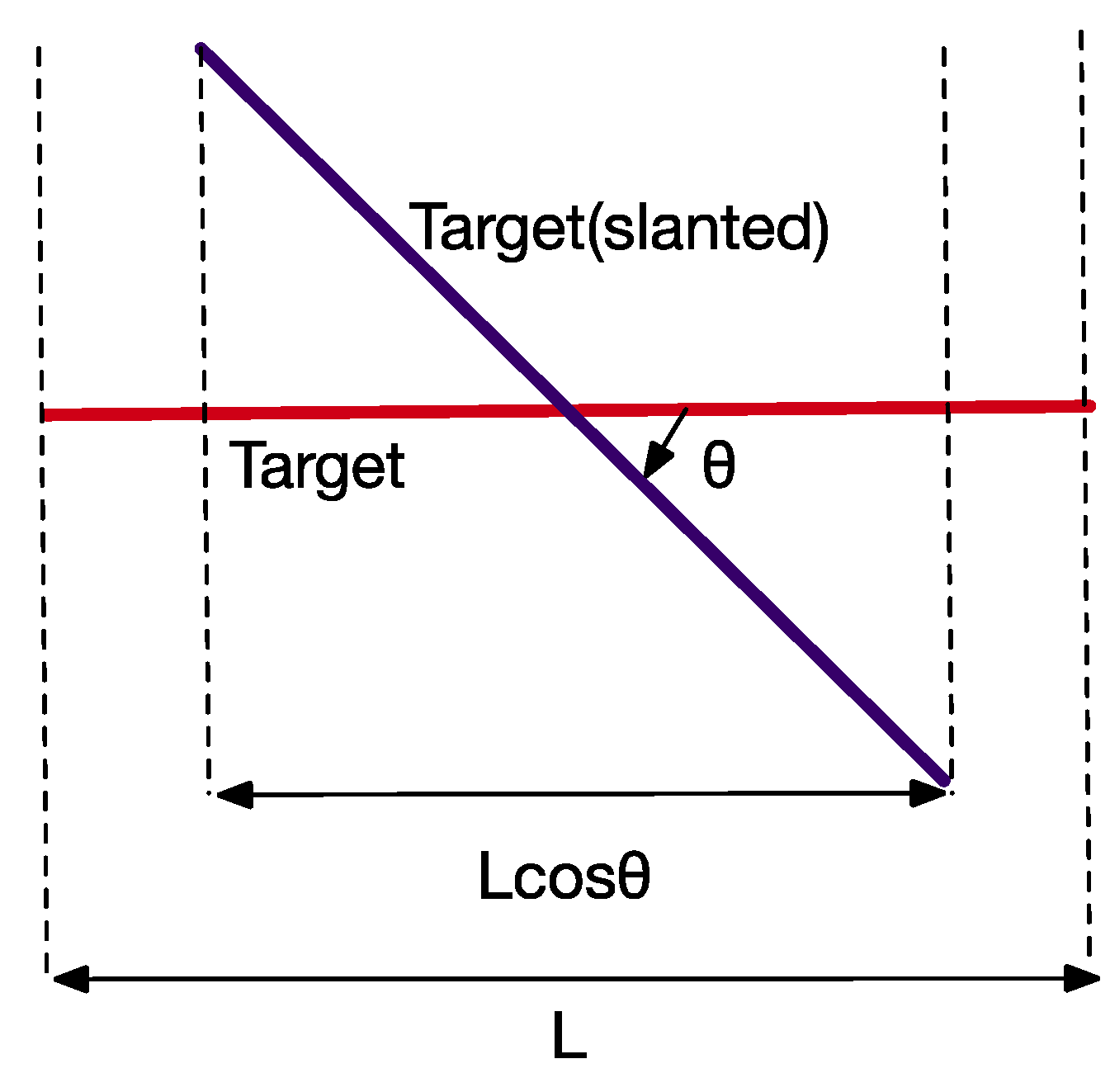
In the case of the GaAs substrate, requirements for the X, Y center coordinates and the area are accommodated within a wide angular range. Any sharp concave-shaped peaks are not noticeable in Figure 13. This suggests that there is no non-diffuse component in reflection from the GaAs substrate. Attitude determination exploiting such a wide angular detection range was investigated. The method utilizes the apparent width of a target of width L, which varies as L c o s θ with the tilt angle θ ( = ϕ 90   d e g ) in Figure 14. Details are described in Appendix D.
.
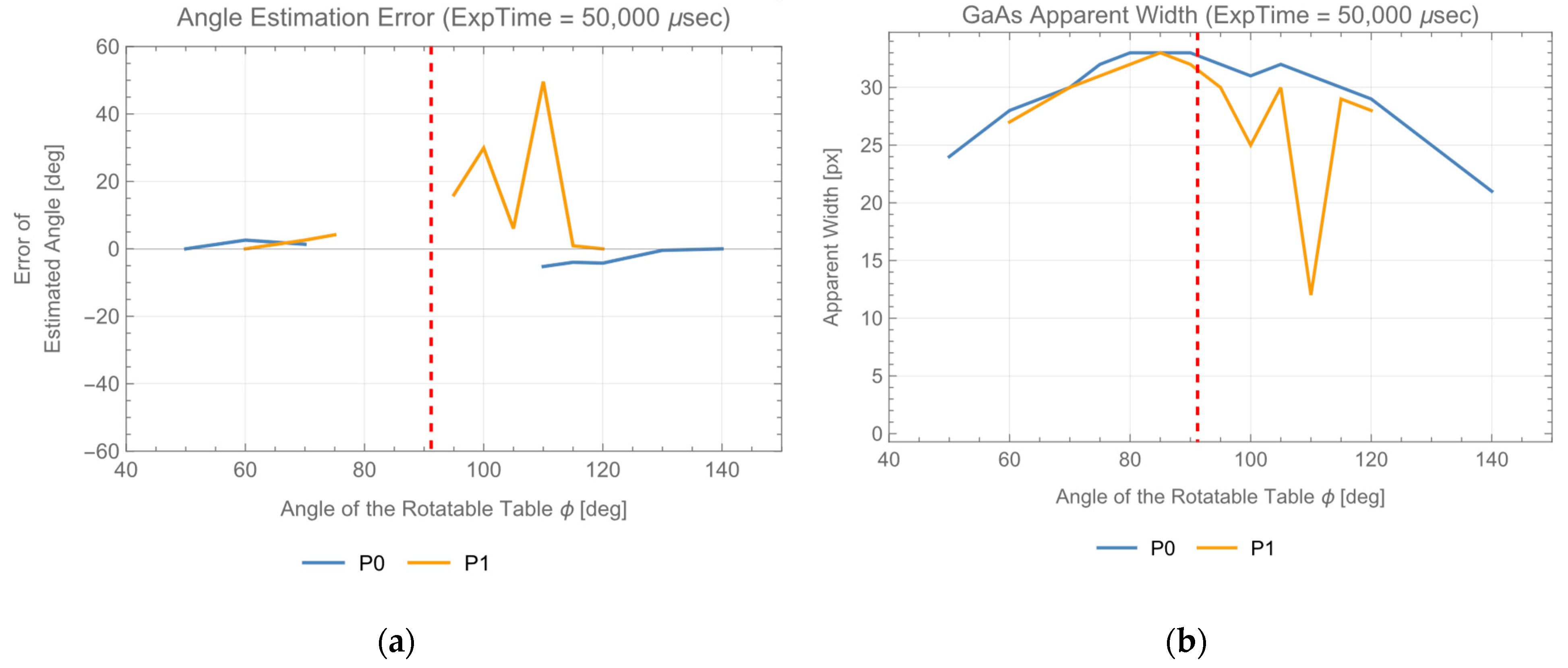
The attitude determination error is shown in Figure 15a, and the estimated apparent width of the GaAs substrate is shown in Figure 15b. The angular center of the rotatable stage is estimated as ϕ = 91.2 degrees from P0 data and 91.8 degrees from P1 data. They are included in Figure 15 as a vertical red dashed line. Attitude determination fails or becomes erroneous within about ±20 degrees near the normal. Excluding this difficulty, the diffuse target’s detectability criteria would be satisfied within a wide angular range from the normal regardless of cooperative or non-cooperative OWPT. One of the reasons for this near-normal difficulty in the diffuse experiment is that variation of the apparent width becomes small near the angular center of the rotatable stage. The other would be that Fresnel reflection from the front surface becomes saturated or dominant, and this causes difficulty in observation of reflected λ O F F beam from the rear surface. In the region around the normal, its attitude determination may cause an error of about ±20 degrees. Compared with the requirement of ±645 mrad (37 degrees) within 100 m target-receiver distance based on the power generation ratio [7], this error is still within the requirement.
In Figure 15b, the width of the GaAs substrate is stably determined in the P0 image except for a little increment of error at 100 degrees. Therefore, failure of attitude determination in the range 75~105 degrees would be caused by the small variation of apparent width. Regarding P1 data, the error became large in the 100~110 degrees range due to failure of determination of the apparent width. By the way, Figure 12 shows the non-diffuse reflection characteristics of the rear surface of the real GaAs solar cell, and strong reflection from the rear surface is observed in the 90~110 degrees range. Since the layouts are the same for the two experiments, both angular ranges are quite similar. Even though non-diffuse solid reflection comes from the rear surface, which helps solar cell detection, a parallel reflection comes from the front surface in the GaAs substrate experiment. Such strong reflection caused difficulty in observing reflection from the rear surface. As a result, determination of the apparent width would have failed. Irradiation by the transmitter assembly used in the experiments causes strong non-diffuse reflection from the front surface. Its effect does not appear uniformly over the entire GaAs substrate, but causes a mottled pattern of saturation. These degrades observation of rear surface reflection in some partial areas. For example, in P0 data, apparent width was successfully estimated by incomplete information from the area where reflection from the rear surface was observed. However, in P1, due to lower irradiation (reflection) level than in the P0, the estimation failed. This would be the reason that causes the significant difference in apparent width determination in P0 and P1 at ϕ = 110 degrees. The front surface of the GaAs substrate used in the experiments is not anti-reflection treated. The issue coming from the strong non-diffuse reflection of the front surface would be improved by anti-reflection treatment. On the other hand, failure of attitude determination below 90 degrees would come from the small apparent width variation like in P0.

6. Conclusions

In this study, a GaAs substrate simulating a solar cell and a real thin-film GaAs solar cell were detected using two infrared wavelengths 850 nm and 940 nm. The ‘threshold equation ‘, which holds at threshold regardless of wavelength, was derived and verified by experimental data.
In OWPT, there would be non-diffuse and diffuse options for the rear surface treatment of solar cell that affects the reflection of λ O F F . The real GaAs solar cell used in the experiments mainly has a non-diffuse reflection characteristic accompanied by diffuse one. In this case, since the center coordinates can be determined within a wide angular range, the existence of the solar cell can be determined. The area of the solar cell can be determined within ±10 degrees around its normal. Its normality can be detected by exploiting this feature. For diffuse targets, the GaAs substrate used in these experiments, both the center coordinates and the area can be determined within a wide angular range. Therefore, attitude can be determined accurately for a large angle from its normal.
One of the issues in solar cell detection using differential absorption imaging is the difficulty of observing λ O F F reflection from its rear surface in the presence of strong λ O N and λ O F F reflection from its front surface. It should be recommended for solar cells for OWPT use that front surface reflection should be reduced for both λ O N and λ O F F . For both non-diffuse and diffuse targets, surface anti-reflection treatment improves this issue.
There would be an OWPT system which utilizes other solar cell materials. Wavelengths used in differential imaging and detail of reflection characteristics of solar cells in this report would be different in other state-of-the-art solar cell materials. However, even though each parameter takes a different value in other OWPT systems, experiments and analyses conducted in this report are still applicable. This study would be a step towards operational OWPT social infrastructure.
Author Contributions

Conceptualization, K.A. and T.M.; methodology, K.A. and T.M.; formal analysis, K.A.; investigation, K.A. data curation, K.A.; software, K.A.; writing—original draft preparation, K.A.; writing—review and editing, T.M.; project administration, T.M.; funding acquisition, T.M. All authors have read and agreed to the published version of the manuscript.

Funding

This work was partially supported by the Tsurugi-Photonics Foundation (No. 20220502) and the Takahashi Industrial and Economic Research Foundation (No. I2-003-13). In addition, part of this paper is based on the project commissioned based on the Mechanical Social Systems Foundation and Optoelectronics Industry and Technology Development Association (“Formulation of strategies for market development of optical wireless power transmission systems for small mobilities”).

Institutional Review Board Statement

Not applicable.

Informed Consent Statement

Not applicable.

Data Availability Statement

Not applicable.

Acknowledgments

We thank Kenta Moriyama and members in the T. Miyamoto Lab for discussion and assistance.

Conflicts of Interest

The authors declare no conflict of interest.

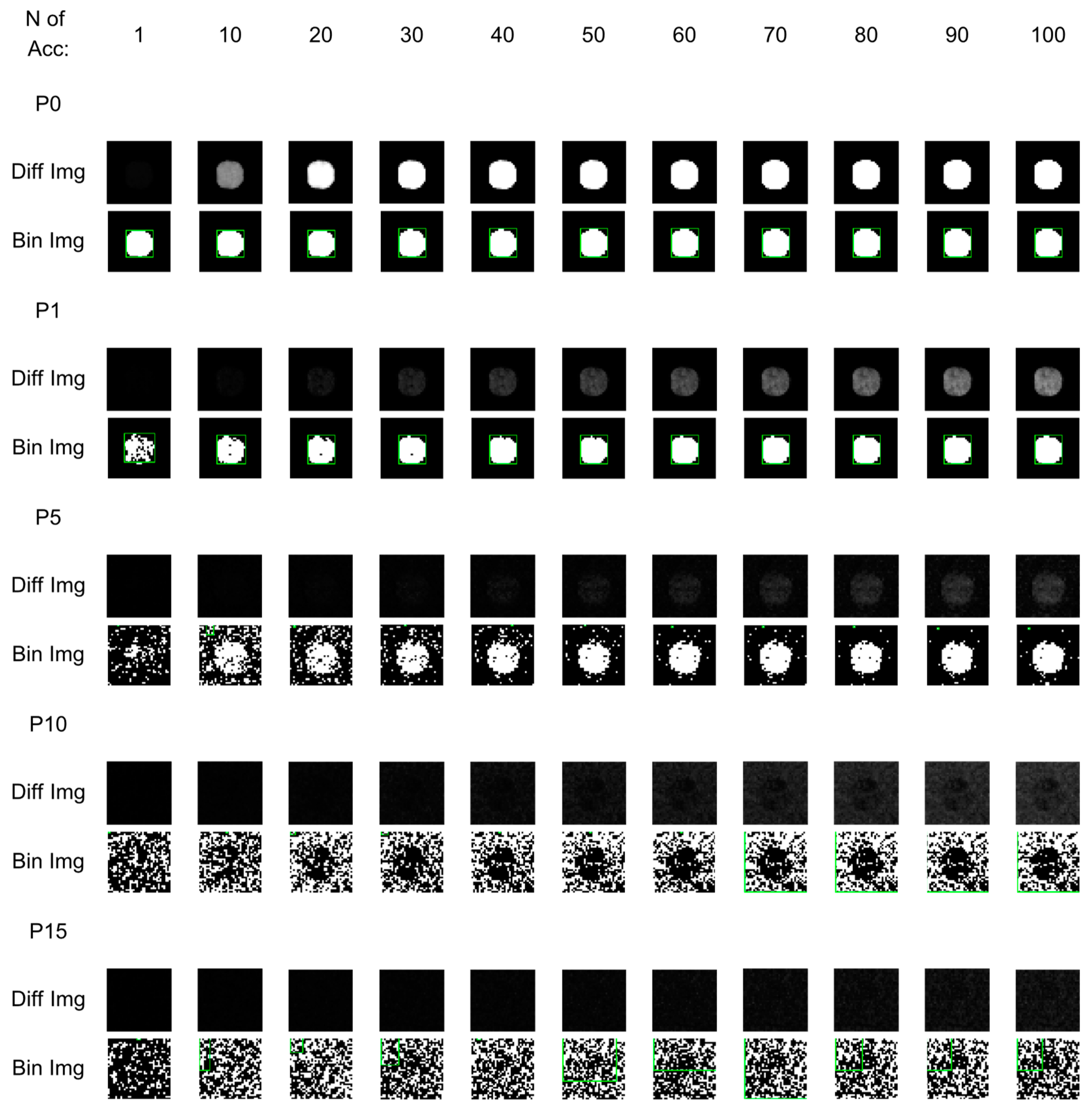
Appendix A. Excerpt from Data Reduction Products (Example of Differential Image, Binarized Image of GaAs Substrate)

Figure A1. Example of differential, binarized image of GaAs substrate. Upper row: Differential image, Lower row: Binarized image, trimming size: 34 × 33 px, Exposure time: 25,000 μs, Horizontal: Number of accumulation (from left to right: 1, 10, 20, 30, 40, 50, 60, 70, 80, 90, 100 times) Highlight in the binarized image represents boundary rectangle of connected components which has the largest area.
Photonics 10 00553 g0a1

Appendix B. Estimation of Diffuse Reflectivity of Si, GaAs Substrate

In the experiments of differential absorption imaging using visible light, λ O N image was generated by irradiating λ = 532 nm to a Si substrate attached to a frost glass. Similarly, simulated λ O F F image was generated by irradiating the same beam to the frost glass. Si image was generated from a differential image of these two. On the other hand, in infrared experiments, λ O N image was generated by irradiating λ = 850 nm to a GaAs substrate attached to a frost glass. λ O F F image was generated by irradiating λ = 940 nm beam to the same target. Both visible and infrared images, brightness at the position of Si or GaAs in λ O N image is negligibly low because λ O N would be strongly absorbed by these substrates.
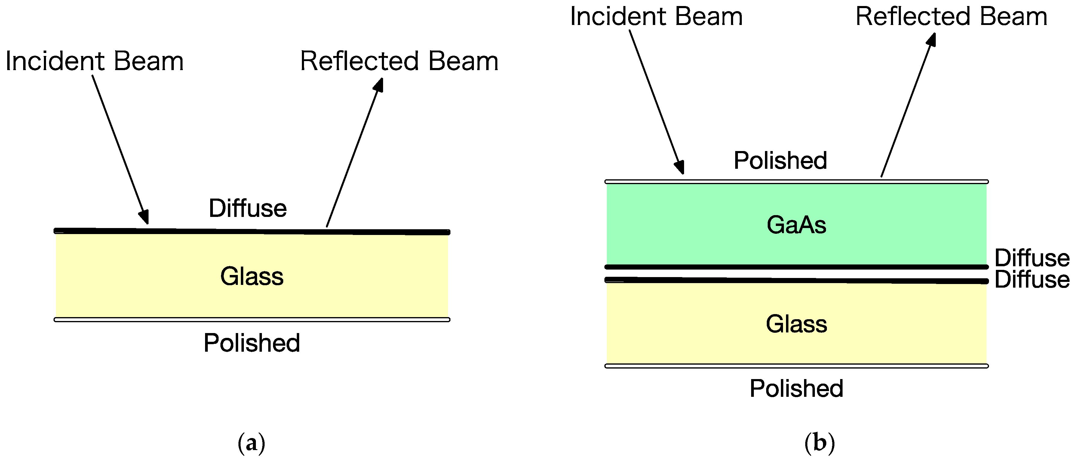
Brightness at the position of these substrates in λ O F F image affects contrast in differential images. It is affected by the frost glass diffuse reflectivity in the visible light experiments, shown in Figure A2a. In infrared experiments, it is affected by reflectivity of the composite target of a GaAs and a frost glass shown in Figure A2b, each material consists of diffuse and polished surfaces. This appendix estimates the reflectivity of such targets for λ = 532 nm and λ = 940 nm based on the Fresnel reflection formula and assumption of Lambertian diffuse surface. The following notation is used throughout this section. When the entrance surface of the ray is polished (P) and the exit surface is diffuse (D), such medium is denoted as ‘PD’. Using such notation, medium in Figure A2a is denoted as DP and composite media in Figure A2b is denoted as ‘PDDP’.
Figure A2. Samples used in the experiments (a) Frost glass sample used in visible experiments; (b) GaAs/Frost glass sample used in infrared experiments.
Photonics 10 00553 g0a2
  • Reflectivity model ( R D P ) of material of DP surfaces
Assume that light enters the medium of index n t whose front surface is diffuse and rear surface is polished from the medium of the index n i with incident angle θ i , and that absorption in each medium is negligible. A light ray entering the front surface is randomly reflected and transmitted (diffused) in various directions. Each diffused ray is Fresnel reflected at the rear surface. Instead of tracing each ray, the reflectivity model is constructed such that the diffuse reflection of the front surface and the Fresnel reflection of diffused ray at the rear surface are replaced by mean values of each ray’s reflectivity over the whole beam.
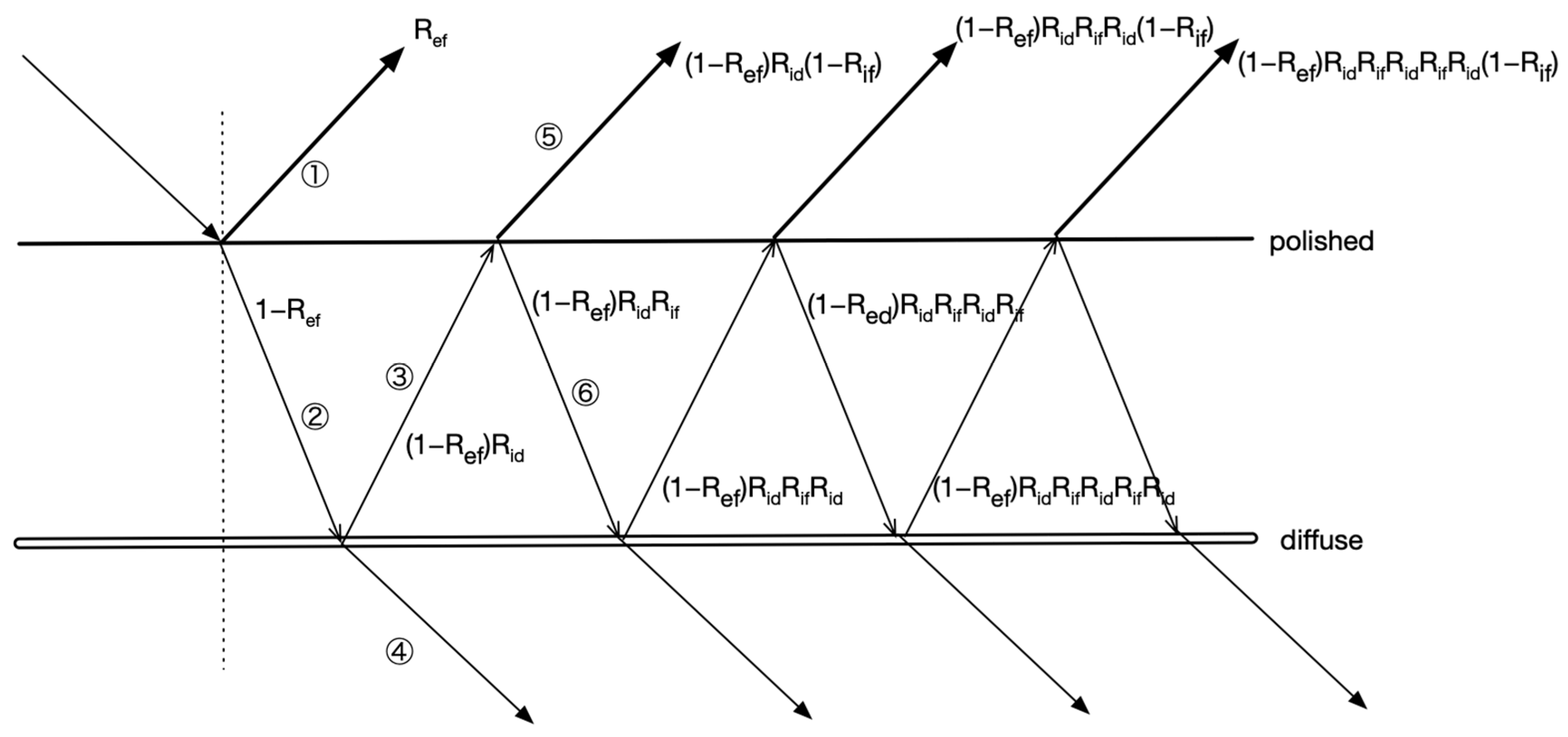
In Figure A3, the ray entering the front surface is divided by a component diffusely reflected at the front surface ① and a component which transmits to the inside of the medium ②. Then, ② is divided by a component which is Fresnel reflected at the rear surface ③ and a component which escapes to the outside of the medium ④. ③ is divided by a component that escapes to the outside ⑤ and a component that is diffusely reflected inside the medium ⑥.
Figure A3. Reflectivity model of DP surface.
Photonics 10 00553 g0a3
2.
Diffuse reflectivity model ( R e d , R i d )
The diffuse surface is modeled as a set of many micro facets, and each facet reflects rays following the Fresnel formula. Each facet has its tilt angle to the surface normal, and the tilt angle is distributed as Gaussian like models in [30,31]. Diffuse reflectivity is calculated by averaging the Fresnel reflectivity of each facet. Fresnel (power) reflectivity averaged over p, s polarization is denoted as R n i , n t , θ i . Then, R e d n i , n t , R i d n t , n i in Figure A3 can be written as
R e d n i , n t = 0 π 2 R n i , n t , θ e x p θ 2 2 σ 2 d θ / 0 π 2 e x p θ 2 2 σ 2 d θ
R i d n t , n i = 0 π 2 R n t , n i , θ e x p θ 2 2 σ 2 d θ / 0 π 2 e x p θ 2 2 σ 2 d θ
3.
Reflectivity model of diffused rays ( R i f )
Assume the radiance of diffusely transmitted ray is Lambertian. The model is constructed such that diffused ray with random incident angle is Fresnel reflected.
R i f n t , n i = 0 π 2 R n t , n i , θ c o s θ s i n θ d θ / 0 π 2 c o s θ s i n θ d θ
4.
Calculation of reflectivity model ( R D P )
R D P can be calculated by summing all components escaping from the front surface in Figure A3.
R D P n i , n t = R e d + 1 R e d R i f 1 R i d + 1 R e d R i f R i d R i f 1 R i d + 1 R e d R i f R i d R i f R i d R i f 1 R i d + = R e d + 1 R e d R i f 1 R i d / 1 R i d R i f
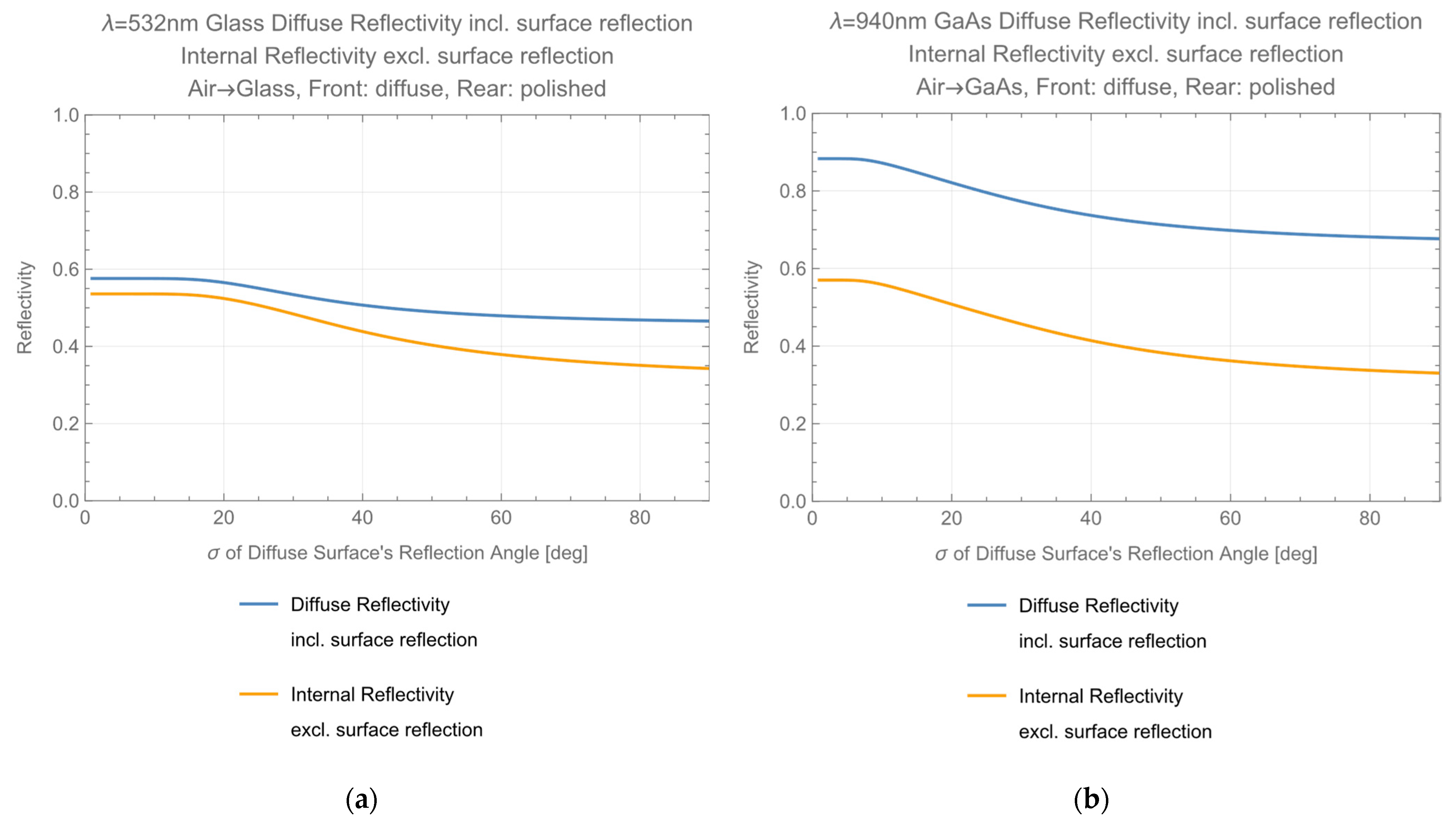
Figure A4 shows calculation for glass ( λ = 532   n m , n i = 1, n t = 1.5), for GaAs ( λ = 940   n m , n i = 1, n t = 3.54) with σ as parameter. In Figure A4, ‘Diffuse Reflectivity’ refers to the calculation of R D P , and ‘Internal Reflectivity’ refers to the second term of R D P . The difference between ‘Diffuse Reflectivity’ and ‘Internal Reflectivity’ in GaAs is larger than glass. This reflects a difference of index between glass and GaAs.
Figure A4. Reflectivity model of DP surface R D P (a) Glass; (b) GaAs..
Photonics 10 00553 g0a4
5.
The reflectivity model ( R P D ) of the material consists of PD surfaces
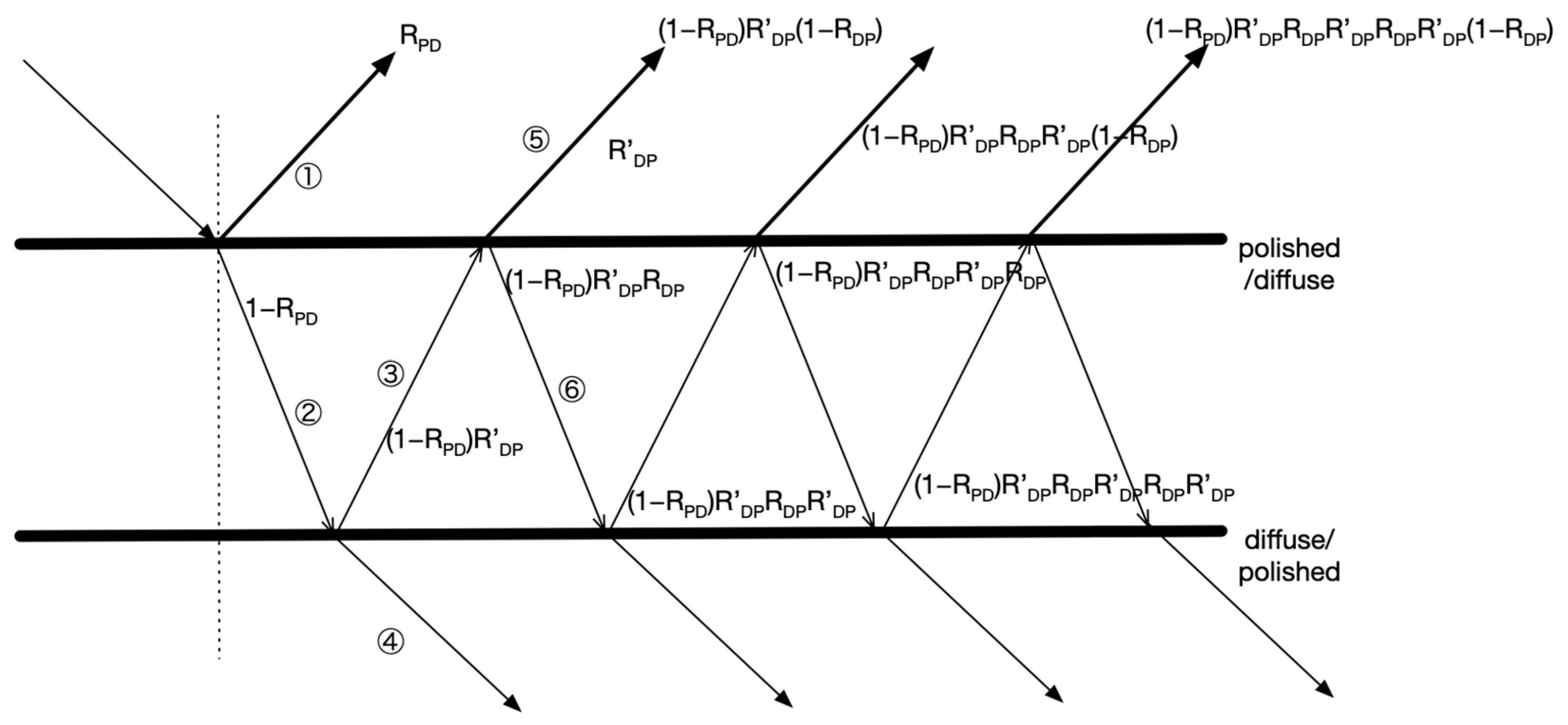
The model can be constructed similarly. Reflectivity model R P D of PD surface is obtained by summing over components escaping from the front surface in Figure A5.
R P D n t , n i , θ = R e f + 1 R e f R i d 1 R i f + 1 R e f R i d R i f R i d 1 R i f + 1 R e f R i d R i f R i d R i f R i d 1 R i f + = R e f + 1 R e f R i d 1 R i f / 1 R i f R i d
R e f is Fresnel reflectivity at the polished front surface, R i f is the internal Fresnel reflection of diffused rays at the polished front surface described in Equation (A3).
R e f = R n i , n t , θ
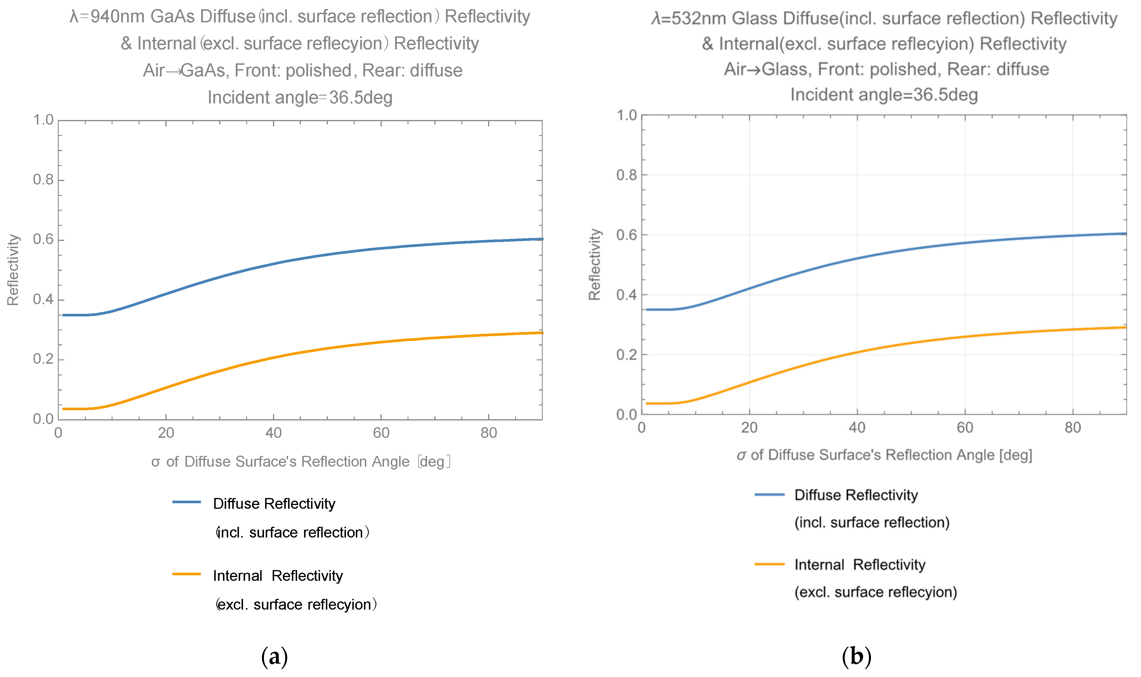
Figure A6 shows the calculation for glass and GaAs. Since the entrance surface is polished, reflectivity depends on the incident angle—the incident angle θ = 36.5 degrees following the infrared experiments.
Figure A5. Reflectivity model of PD surface.
Photonics 10 00553 g0a5
Figure A6. Reflectivity model of PD surface R P D (a) Glass; (b) GaAs.
Photonics 10 00553 g0a6
Like R D P , the difference between ‘Diffuse Reflectivity’ and ‘Internal Reflectivity’ in GaAs is larger than in glass. Especially in GaAs, it should be noted that the main part of ‘Diffuse Reflectivity’ comes from surface reflection and the internal reflection part is within 10~20% range for σ = 20~40 degrees.
6.
Reflectivity model ( R P D D P ) of PDDP composite surface
To simulate infrared experiments, assume the ray enters composite medium from the air of index n i = 1. The medium consists of medium1 and medium2. The medium1 (index n t ) has a PD surface, and the medium2 (index n t ) has a DP surface.
The reflectivity of medium1 is denoted as R P D . Similarly, the reflectivity of medium2 is denoted as R D P in case that ray enters from a diffuse surface. There would be rays that escaped from the polished surface of medium2 and reenters. Such rays’ contributions are ignored.
Considering Figure A3 and Figure A5, the reflectivity of composite media R P D D P can be calculated from Figure A7 and expressed as,
R P D D P n i , n t , θ = R P D n i , n t , θ + 1 R P D n i , n t , θ R D P n i , n t 1 R D P n i , n t / 1 R D P n i , n t R D P n i , n t
Figure A7. Reflectivity model of composite PDDP surfaces.
Photonics 10 00553 g0a7
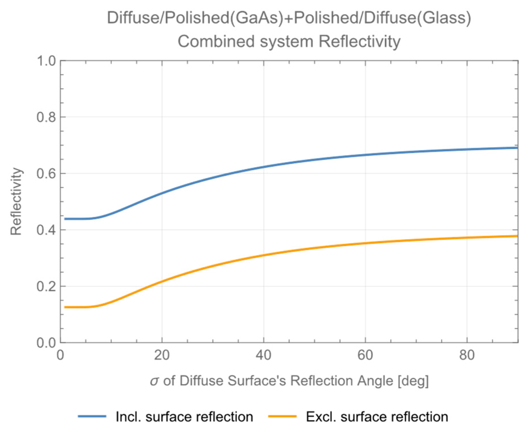
Figure A8 shows the reflectivity calculation of composite media consisting of GaAs PD and glass DP surface. Calculations are for both cases of including Fresnel reflection from the front surface and excluding such Fresnel components.
Figure A8. The reflectivity of composite media consisting of GaAs PD and glass DP surfaces.
Photonics 10 00553 g0a8
7.
The ratio of diffuse reflectivity of visible experiments to infrared
ρ 532 in (8) is identified as R D P ( G l a s s ) and ρ 940 as R P D D P G a A s / G l a s s . From Figure 11, R P D D P ( G a A s / G l a s s ) = 0.2~0.3 within σ = 20~30 degrees range [30]. Since R D P ( G l a s s ) = 0.5~0.55, therefore, their ratio is estimated to be
ρ 532 ρ 940 = R D P G l a s s R P D D P G a A s / G l a s s 1.7 ~ 2.75

Appendix C. Excerpt from Data Reduction Products (Example of Differential Image, Binarized Image of GaAs Solar Cell)

Figure A9. Examples of solar cell detection. From upper row to lower row: λ O N image, λ O F F image, Differential image, Binarized image, Trimming size: 82 × 83 px, Power control status P0. The binarization threshold was set to 1/255. Exposure time: 25, 50, 100, 250, 500, 1000, 2500, 5000, 10,000, 25,000, 50,000, 100,000, 200,000 μs. The binarized image’s highlight represents the boundary rectangle of connected components which has the largest area. This example shows the case of the rotatable stage angle ϕ = 100 degrees, and the solar cell is stably detected from exposure time 25 μs.
Photonics 10 00553 g0a9

Appendix D. Attitude Determination by Mean of Variation of Apparent Width of Target

The attitude of the detected GaAs substrate is determined using a variation of its apparent width. Assume the full width of the target is L 0 , then, apparent with is L 0 c o s θ for tilt angle θ in Figure 14, and this is equal to the observed target width L o b s ( θ ) .
L o b s θ = L 0 c o s θ
Even though L o b s θ cannot be distinguished from L o b s θ in this attitude determination method, the state of tilt angle θ and that of tile angle θ are equivalent from the transmitter’s beam shaping point of view. This does not cause any difficulty in actual operation when the transmitter’s optical axis is parallel to the receiver’s.
In the experiments conducted, since these two axes are not parallel, the experiment system does not have exact symmetry. Due to this asymmetry, strong surface reflection occurs at around ϕ 110 ( θ 20) degrees described in Section 5.
Since L o b s θ includes observation error, it generally does not coincide with L 0 c o s θ . When θ varies from 0 (zero), variation of the apparent width L 0 c o s θ is small near θ = 0 . The variation becomes larger with increment of θ . In the case of P0, the GaAs substrate was detected within ϕ = 50~140 degrees angular range. At both endpoints ϕ = 50, 140 degrees, detection of such variation would become more accurate than near the center whose variation is smaller. Therefore, it is assumed that the determination of the apparent width at ϕ = 50, 140 degrees are accurate enough and that the following equations hold with enough accuracy.
L o b s 50 ° ϕ 0 = L 0 c o s 50 ° ϕ 0
L o b s 140 ° ϕ 0 = L 0 c o s 140 ° ϕ 0
Here ϕ 0 is the exact center angle of the rotatable stage.
From (A10) and (A11),
L o b s 50 ° ϕ 0 / L o b s 140 ° ϕ 0 = c o s 50 ° ϕ 0 / c o s 140 ° ϕ 0
The left-hand side is ratio of the apparent width of the target at ϕ = 50 degrees to the one at ϕ = 140 degrees, and this is determined by the experiment data. From (A10) or (A11) and (A12), L 0 can be estimated. From the P0 experiment data, estimations are ϕ 0 = 91.9 degrees and L 0 = 31.9 px. In P1 data, GaAs substrate was detected within ϕ = 60~120 degrees angular range. In this case, estimations are ϕ 0 = 91.8 degrees and L 0 = 31.9 px. Using these estimations and the determined value of the apparent width L o b s ϕ ϕ 0 , ϕ ^ can be estimated as,
ϕ ^ = c o s 1 L o b s ϕ ϕ 0 / L 0 θ ϕ ϕ 0 c o s 1 L o b s ϕ ϕ 0 / L 0 θ ϕ 0 ϕ + ϕ 0 where   θ x = 1   f o r   x 0 0   f o r   x < 0
Figure 15a shows the plot for ϕ ^ ϕ .

References

  1. Frolova, E.; Dobroskok, N.; Morozov, A. Critical Review of Wireless Electromagnetic Power Transmission Methods. In Proceedings of the International Scientific and Practical Conference “Young Engineers of the Fuel and Energy Complex: Developing the Energy Agenda of the Future” (EAF 2021), Saint-Petersburg, Russia, 10–11 December 2021; Atlantis Press International B.V: Amsterdam, The Netherlands, 2022. [Google Scholar] [CrossRef]
  2. Liu, Q.; Xiong, M.; Liu, M.; Jiang, Q.; Fang, W.; Bai, Y. Charging A Smartphone Over the Air: The Resonant Beam Charging Method. IEEE Internet Things J. 2022, 9, 13876–13885. [Google Scholar] [CrossRef]
  3. The Wireless Power Company. Wi-Charge. Available online: https://www.wi-charge.com (accessed on 9 May 2022).
  4. PowerLight Technologies. Available online: https://powerlighttech.com/ (accessed on 23 May 2022).
  5. Landis, G.A. Laser Power Beaming for Lunar Polar Exploration. In Proceedings of the AIAA Propulsion and Energy 2020 Forum, Virtual Event, 24–28 August 2020; American Institute of Aeronautics and Astronautics: Reston, VA, USA, 2020. [Google Scholar] [CrossRef]
  6. Wang, J.-X.; Zhong, M.; Wu, Z.; Guo, M.; Liang, X.; Qi, B. Ground-based investigation of a directional, flexible, and wireless concentrated solar energy transmission system. Appl. Energy 2022, 322, 119517. [Google Scholar] [CrossRef]
  7. Baraskar, A.; Yoshimura, Y.; Nagasaki, S.; Hanada, T. Space solar power satellite for the Moon and Mars mission. J. Space Saf. Eng. 2022, 9, 96–105. [Google Scholar] [CrossRef]
  8. Lee, N.; Blanchard, J.T.; Kawamura, K.; Weldon, B.; Ying, M.; Young, S.A.; Close, S. Supporting Uranus Exploration with Deployable ChipSat Probes. In Proceedings of the AIAA SCITECH 2022 Forum, San Diego, CA, USA & Virtual, 3–7 January 2022; American Institute of Aeronautics and Astronautics: Reston, VA, USA, 2022. [Google Scholar] [CrossRef]
  9. Asaba, K.; Miyamoto, T. System Level Requirement Analysis of Beam Alignment and Shaping for Optical Wireless Power Transmission System by Semi–Empirical Simulation. Photonics 2022, 9, 452. [Google Scholar] [CrossRef]
  10. Asaba, K.; Miyamoto, T. Relaxation of Beam Irradiation Accuracy of Cooperative Optical Wireless Power Transmission in Terms of Fly Eye Module with Beam Confinement Mechanism. Photonics 2022, 9, 995. [Google Scholar] [CrossRef]
  11. Putra, A.W.S.; Kato, H.; Maruyama, T. Infrared LED marker for target recognition in indoor and outdoor applications of optical wireless power transmission system. Jpn. J. Appl. Phys. 2020, 59, SOOD06. [Google Scholar] [CrossRef]
  12. Imai, H.; Watanabe, N.; Chujo, K.; Hayashi, H.; Yamauchi, A.A. Beam-Tracking Technology Developed for Free-Space Optical Communication and Its Application to Optical Wireless Power Transfer. In Proceedings of the 4th Optical Wireless and Fiber Power Transmission Conference (OWPT2022), Yokohama, Japan, 18–21 April 2022. [Google Scholar]
  13. Differential Absorption Lidar|Elsevier Enhanced Reader. Available online: https://reader.elsevier.com/reader/sd/pii/B9780123822253002048?token=ACBBE2F8761774F5628FC13C0F6B8E339140949E50BF9DE9F5063F95873CC081FB2353E862E10CA4576416252562C600&originRegion=us-east-1&originCreation=20220824035349 (accessed on 24 August 2022).
  14. Dual-Wavelength Measurements Compensate for Optical Interference|7 May 2004. Available online: https://www.biotek.com/resources/technical-notes/dual-wavelength-measurements-compensate-for-optical-interference/ (accessed on 24 August 2022).
  15. Herrlin, K.; Tillman, C.; Grätz, M.; Olsson, C.; Pettersson, H.; Svahn, G.; Wahlström, C.-G.; Svanberg, S. Contrast-enhanced radiography by differential absorption, using a laser-produced X-ray source. Investig. Radiol. 1997, 32, 306–310. [Google Scholar] [CrossRef] [PubMed]
  16. Asaba, K.; Moriyama, K.; Miyamoto, T. Preliminary Characterization of Robust Detection Method of Solar Cell Array for Optical Wireless Power Transmission with Differential Absorption Image Sensing. Photonics 2022, 9, 861. [Google Scholar] [CrossRef]
  17. OS13CA5111A. Opto Supply. Available online: https://www.optosupply.com/uppic/20211028118028.pdf (accessed on 29 December 2022).
  18. OSI5FU511C-40. Akizuki Denshi. Available online: https://akizukidenshi.com/download/OSI5FU5111C-40.pdf (accessed on 29 December 2022).
  19. Intel. Intel® RealSenseTM D400 Series Data Sheet Revision 013 April 2022; Intel: Santa Clara, CA, USA, 2022. [Google Scholar]
  20. Intel® RealSenseTM. Intel® RealSenseTM Depth and Tracking Cameras. Available online: https://www.intelrealsense.com/sdk-2/ (accessed on 24 August 2022).
  21. Welcome to Python.org. Python.org. Available online: https://www.python.org/ (accessed on 24 August 2022).
  22. Open CV. OpenCV. Available online: https://opencv.org/ (accessed on 23 August 2022).
  23. Wolfram Mathematica: Modern Technical Computing. Available online: https://www.wolfram.com/mathematica/ (accessed on 15 August 2022).
  24. Otsu, N. A Threshold Selection Method from Gray-Level Histograms. IEEE Trans. Syst. Man Cybern. 1979, 9, 62–66. [Google Scholar] [CrossRef]
  25. Corporate Profile|AXT, Inc. Available online: http://axtinc.gcs-web.com/ (accessed on 14 February 2023).
  26. Mori, N. Design of Projection System for Optical Wireless Power Transmission using Multiple Laser light sources, Fly-eye lenses, and Zoom lens. In Proceedings of the 1st Optical Wireless and Fiber Power Transmission Conference OWPT2019, Yokohama, Japan, 23–25 April 2019; p. OWPT-4-02. [Google Scholar]
  27. Katsuta, Y.; Miyamoto, T. Design, simulation and characterization of fly-eye lens system for optical wireless power transmission. Jpn. J. Appl. Phys. 2019, 58, SJJE02. [Google Scholar] [CrossRef]
  28. Industrial Cameras: Spectral Sensitivity. The Imaging Source. Available online: https://s1-dl.theimagingsource.com/api/2.5/packages/publications/whitepapers-cameras/wpspectsens/a5cb0f39-fea8-56ae-8e04-ec20ab4e72c9/wpspectsens_1.30.en_US.pdf (accessed on 29 December 2022).
  29. Rocket ya Jinkoueisei Tou No Utyukaihatsu to Jinkoueisei Uchiage Sservice No Sentangijyutukaihatu Kenkyujyo Utyukaihatsu. Available online: https://www.ati-space.com/ATI.files/company.htm (accessed on 15 February 2023).
  30. Oren, M.; Nayar, S.K. Generalization of Lambert’s reflectance model. In Proceedings of the 21st Annual Conference on Computer Graphics and Interactive Techniques—SIGGRAPH ’94, Orlando, FL, USA, 24–29 July 1994; ACM Press: New York, NY, USA, 1994; pp. 239–246. [Google Scholar] [CrossRef]
  31. Torrance, K.E.; Sparrow, E.M. Theory for Off-Specular Reflection From Roughened Surfaces. JOSA 1967, 57, 1105–1114. [Google Scholar] [CrossRef]
Figure 1. Principle of differential absorption imaging.
Photonics 10 00553 g001
Figure 2. The configuration and layout of the experiment (a) Configuration; (b) Layout of the experiment.
Photonics 10 00553 g002
Figure 3. Infrared GaAs substrate image (a) λ O F F image; (b) λ O N image; (c) Differential image; (d) Binarized image.
Photonics 10 00553 g003
Figure 4. (a) Center coordinates of the target; (b) Area.
Photonics 10 00553 g004
Figure 5. An example of estimation of the center coordinates and the area of GaAs substrate (a) X center coordinate; (b) Y center coordinate; (c) Area.
Photonics 10 00553 g005aPhotonics 10 00553 g005b
Figure 6. Mean signal level ( I T G T ) and mean background level ( I B G ).
Photonics 10 00553 g006
Figure 7. The normalized I d i f f against exposure time (a) data from visible experiments; (b) data from infrared experiments.
Photonics 10 00553 g007
Figure 8. Noise reduction in Binarized Images by Increment of Exposure Time (a) Exposure Time 500 μs; (b) Exposure Time 5000 μs; (c) Exposure Time 50,000 μs; (d) Exposure Time 200,000 μs.
Photonics 10 00553 g008
Figure 9. Layouts and target of the experiments (a) Layout of the Experiments; (b) GaAs Solar Cell.
Photonics 10 00553 g009
Figure 10. Example of captured images (a) λ O N image; (b) λ O F F .
Photonics 10 00553 g010
Figure 11. Determination example of the center coordinates and the area of GaAs solar cell (a) X center coordinate; (b) Y center coordinate; (c) Area.
Photonics 10 00553 g011aPhotonics 10 00553 g011b
Figure 12. Angular dependence of the minimum exposure time for real GaAs solar cell detection, which accommodates the requirements (a) X center coordinate; (b) Y center coordinate; (c) Area.
Photonics 10 00553 g012
Figure 13. Angular dependence of the minimum exposure time for GaAs substrate detection, which accommodates the requirements (a) X center coordinate; (b) Y center coordinate; (c) Area.
Photonics 10 00553 g013
Figure 14. Varying apparent with of target with tilt angle θ .
Photonics 10 00553 g014
Figure 15. Attitude determination of diffuse GaAs substrate (a) Attitude determination error; (b) Estimated apparent width of the GaAs substrate.
Photonics 10 00553 g015
Table 1. The threshold exposure time of visible and infrared experiments.
Power Control
Status
Threshold Exposure Time
in Visible Experiments
Threshold Exposure Time
in Infrared Experiments
Ratio
(Infrared/Visible)
P078 μs1000 μs12.8
P11250 μs15,000 μs12.0
P510,000 μs
Disclaimer/Publisher’s Note: The statements, opinions and data contained in all publications are solely those of the individual author(s) and contributor(s) and not of MDPI and/or the editor(s). MDPI and/or the editor(s) disclaim responsibility for any injury to people or property resulting from any ideas, methods, instructions or products referred to in the content.