Article

Analog Wavelength Locking in an Optical Single-Sideband Transmitter of a Millimeter-Wave Radio-Over-Fiber Link Featuring a Micro-Ring Resonator and a Heat-Pump-Controlled Laser

1
Laboratory of Fundamentals of Electrical Engineering and Electromagnetics, Faculty of Electrical Engineering, University of Ljubljana, Tržaška Cesta 25, 1000 Ljubljana, Slovenia
2
Laboratory of Photovoltaics and Optoelectronics, Faculty of Electrical Engineering, University of Ljubljana, Tržaška Cesta 25, 1000 Ljubljana, Slovenia
3
Radiation and Optics Laboratory, Faculty of Electrical Engineering, University of Ljubljana, Tržaška Cesta 25, 1000 Ljubljana, Slovenia
*
Author to whom correspondence should be addressed.
Photonics 2023, 10(12), 1341; https://doi.org/10.3390/photonics10121341
Submission received: 20 October 2023 / Revised: 24 November 2023 / Accepted: 1 December 2023 / Published: 5 December 2023
(This article belongs to the Section Optical Communication and Network)

Abstract

:
This paper presents a novel approach to addressing the issue of temperature-induced instability in an optical, single-sideband transmitter based on a micro-ring resonator (MRR) suitable for millimeter-wave (mmW) radio-over-fiber (RoF) communications. We propose utilizing the drop port of the MRR to provide a feedback signal to the closed-loop control (CLC) system. The latter serves to maintain the optimal alignment between the laser’s carrier and the MRR’s resonant wavelength, thus mitigating the adverse effects of chromatic-dispersion-induced power fading at the receiving end. Since the feedback information is extracted from the otherwise-wasted resonant energy at the drop port, the control system does not compromise the delicate optical signal at the through port. A CLC was synthesized, designed, and prototyped to provide real-time wavelength tuning of the heat-pump-controlled laser based on the feedback signal. Experimental evaluations demonstrate that the wavelength of the laser could be successfully locked to the MRR’s resonance with a wavelength dither of less than 0.004 nm (~491 MHz). This allowed us to limit the power-penalty deterioration to less than 2 dB for a RoF link with a 2.5-km standard telecommunication single-mode fiber (SMF), a modulation frequency of 37.8 GHz, and a carrier wavelength of 1563.97 nm (~191.820 THz). The proposed solution offers an alternative approach for the carrier and the MRR’s resonant wavelength interlocking without the need for complex photonics like thermo-optic or electro-optic structures to control the temperature or phase velocity, respectively.

1. Introduction

Radio-over-fiber (RoF) links assisted by integrated microwave photonics (MWP) are expected to play an important role in the fifth generation (5G) and beyond [1]. With the ever-increasing demand for higher bandwidths, technologies have moved toward higher-frequency bands, such as the millimeter-wave (mmW) bands [2]. Unfortunately, wireless transmission in the mmW range is limited by the attenuation caused by the non-transparent obstacles and absorption in the atmosphere [3]. Therefore, among other reasons, fiber-based communication is envisioned in certain parts of the future-generation radio access network (RAN) [4,5]. Nevertheless, the well-known advantages of fiber optics, such as low attenuation, extensive bandwidth, immunity to electromagnetic interference, and compatibility with microwave photonic systems, come at a price. When signals in the mmW frequency range are transmitted over standard, single-mode fiber (SMF) in analog RoF (A-RoF) format, such as Intermediate Frequency over Fiber (IFoF) or Radio-Frequency over Fiber (RFoF), the non-zero chromatic dispersion at telecom wavelengths causes group velocity dispersion (GVD). In an intensity-modulated A-RoF link, given its typical double-sideband spectral profile, this causes a relative phase shift between both sidebands and effectively presents us with an unfavorable frequency- and length-dependent power fading [6]. While there are several ways [6,7,8] to mitigate this issue, introducing a two-color signal, such as an optical single-sideband (OSSB) signal [9,10] or an optical double-sideband (ODSB) signal with a suppressed carrier (SC) [11,12,13,14,15], is a robust and universal solution that does not depend on the fiber’s length and can therefore be applied to various optical network topologies, e.g., point-to-multipoint. A wide variety of techniques for establishing a two-color spectral profile has been proposed and demonstrated. However, with advances in photonic-integrated-circuit (PIC) manufacturability, photonic solutions are becoming increasingly attractive. One such example is a simple add/drop micro-ring resonator (MRR) [16], exhibiting a multi-stopband filter response in the input-through direction, which can be used to suppress one of the sidebands in an ODSB modulation scheme, as demonstrated in our previous publication [17]. Several other research papers also report on similar approaches, while using the somewhat more complex MRR-based photonic structures [18,19,20].
This paper further investigates a solution employing an MRR to suppress one of the sidebands and addresses the inherent, yet undesirable, temperature instability of the MRR and its optical transfer function (OTF). MRRs are highly susceptible to temperature fluctuations, with a typical temperature dependence in the range of tens of pm/K for silicon-on-insulator technology [21]. This causes the resonant wavelength(s) to shift over time, worsening the sideband-suppression ratio (SBSR), which reintroduces the power fading. Researchers have investigated different approaches to overcome the challenges of MRR temperature dependence [22]. Existing approaches mostly fall into two categories: (1) approaches that permanently reduce the temperature dependence of MRRs to very low or near-zero values by altering their structural and/or material properties, so-called athermal solutions, and (2) the ones that actively control their instantaneous material and/or geometric properties by means of thermo-optic- (TO) [23,24] or electro-optic- (EO) effect-enabling elements. While athermal solutions might effectively eliminate the temperature dependence of the MRR, it might not guarantee its relative wavelength alignment with the laser of an RoF transmitter. Solutions from the second category rely on some kind of feedback information, reflecting the state of the MRR’s OTF, which is then processed by the control system, acting on the tuning mechanism, e.g., the integrated heaters. The feedback information can be extracted in a few different ways, i.e., either by directly sensing the local temperature of the PIC [25], by monitoring the optical power at the drop port [26,27,28,29,30] or, less conveniently, tapping it from the through port [31], or even analyzing the BER [32] resulting from the instantaneous alignment of the OTF. While the latter metric reflects the transmitter’s performance most relevantly in telecommunication terms, it requires a complex, high-speed monitoring and control system. There is yet another potential approach to extracting the feedback information that relies on detecting the phase response of the MRR’s OTF. Unfortunately, such an approach requires precise interferometric measurements that need to be implemented at the scale of a PIC. With the feedback signal sorted, a variety of mechanisms for tuning the OTF accordingly has been proposed and demonstrated. Some are employing integrated resistive heaters [26,27,33], then others indirectly control the temperature by adjusting the bias current of the diode junction [31,34] (applicable to carrier injection micro-ring modulators) and then there are also some solutions that rely on the EO effect [35,36].
Our solution would fall into the second category, while tackling the challenge from a different angle. Since only the relative alignment of the carrier wavelength and the MRR’s OTF are important for maintaining the maximum SBSR, we propose tuning the carrier wavelength, e.g., of a heat-pump-controlled laser, instead. Unlike some other approaches monitoring the MRR’s temperature, we extract the feedback signal by continuously measuring the optical power at the drop port, which directly reflects the state of the wavelength’s (mis)alignment. An advantage is that this approach does not rely on complex photonic structures, enabling the manipulation of the MRR’s characteristics. Rather, it employs a basic add/drop MRR with no additional features and a common distributed feedback (DFB) laser, an inherently necessary device, with heat-pump-enabled wavelength tuning. To the best of our knowledge, no research has been conducted to address this challenge, respectively.
The rest of this paper is organized as follows. In Section 2, a theoretical background of the dispersion-induced power penalty (PP), an MRR-enabled mitigation approach, the MRR’s temperature dependence and a proposed solution to the latter are presented. A potential solution, i.e., a closed-loop control (CLC) system, is synthesized, designed and the corresponding prototype manufactured to accommodate the experimental evaluation followed in Section 3. There, the evaluation metrics are declared, the experimental setup(s) are described, and the acquired results are presented. In Section 4, we evaluate the significance of the results and their implications. Finally, in Section 5, we conclude the paper and give possible future directions for research and practical applications.

2. Theory, Requirements and Synthesis

2.1. Dispersion-Induced Power Fading

With many unbeatable advantages as a transmission medium, SMF, similar to any waveguide (WG) system, is prone to dispersion. Besides WG dispersion, which is also present in other (hollow) WG structures, in optical fibers the material itself is also dispersive (wavelength-dependent refractive index). In a standard telecommunications fiber (e.g., G.652), both terms effectively cancel out at a wavelength of 1310 nm, whereas at an increasingly exploited wavelength of 1550 nm, such a fiber exhibits a non-zero dispersion with a dispersion coefficient of D 17   p s / ( n m k m ) . This results in a so-called group velocity dispersion (GVD)—different frequency components experience different delays—causing the effect of pulse broadening and intersymbol interference in digital communications or RF power fading when radio-over-fiber communications are considered. This paper focuses on the latter manifestation of essentially the same phenomenon.
Power fading can (analytically) be represented by the PP function (of two variables, i.e., fiber length L and modulation frequency f R F ), which is basically given as the ratio of the optical powers at the receiving end and that from the transmitting end of the RoF link, as per Equation (13) in [8]
P P 0 d B = 10 log 10 cos 2 π λ 2 c 0 D f R F 2 L ,
where λ stands for the laser carrier wavelength and c 0 is the speed of light in vacuum. Note that all the wavelengths mentioned in this paper are expressed as the wavelengths in free space. Figure 4 in [17] shows the PP function in a 2D color plot, showing multiple regions (i.e., combinations of L and f R F ) with extensive attenuation of the RF signal due to the unfavorable PP value. Clearly, as this arises from two interfering sidebands, eliminating one of the two sidebands overcomes the issue. This can be approached by employing an appropriate optical bandstop filter such as an MRR on a PIC, e.g., [37].

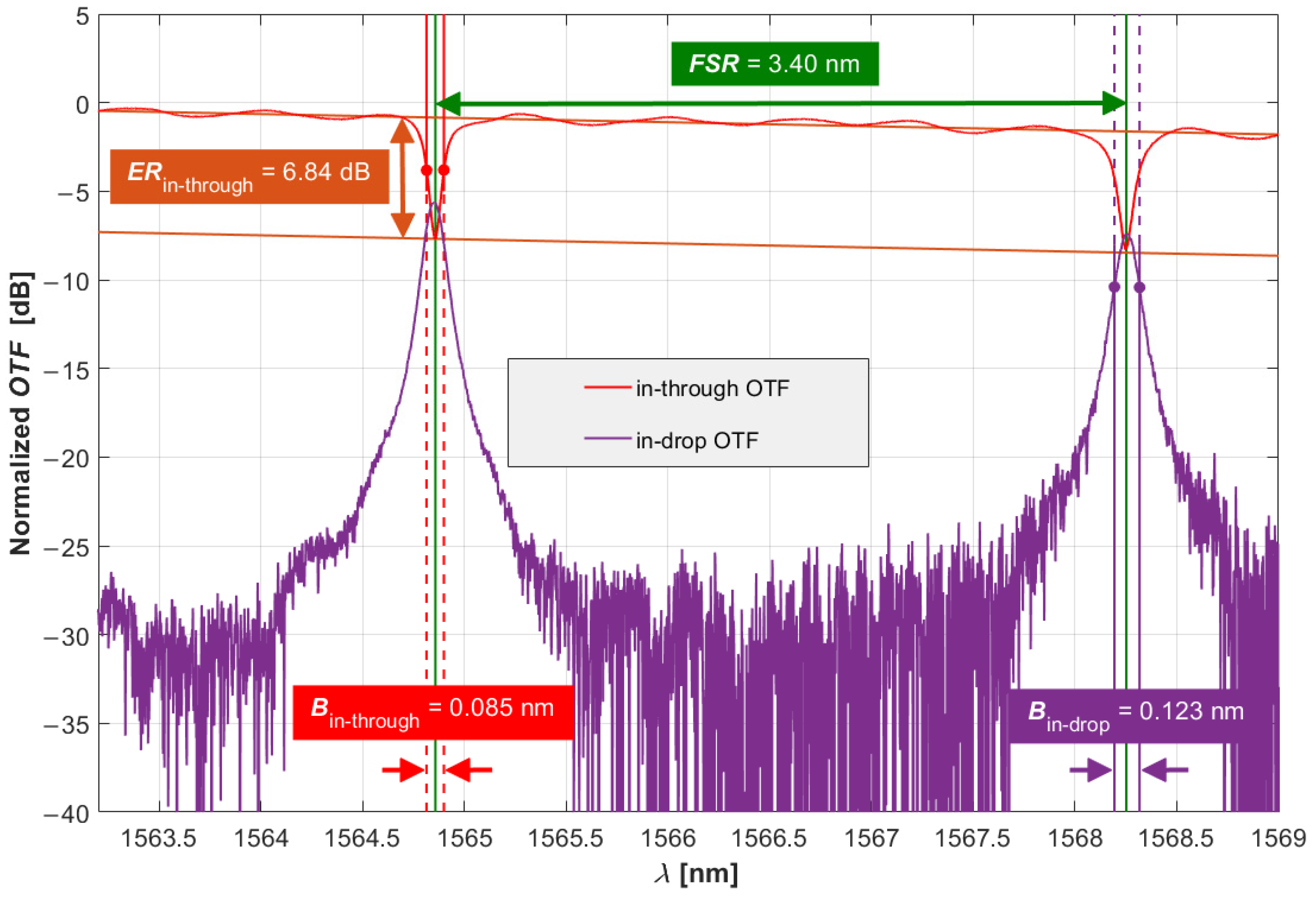
2.2. Micro-Ring Resonator as a Bandstop Filter

While there are multiple approaches to overcoming chromatic-dispersion-induced power fading in RoF links, this paper investigates an approach from the rapidly expanding field of MWP. With well-known advantages such as the independence of the radio frequency, excessive bandwidth capabilities, low attenuation, immunity to EMI, reconfigurability, MWP offers new solutions for RF signal (in the microwave and mmW ranges) generation, detection and/or processing. Furthermore, with integrated photonics and narrow bandwidth laser sources coherent applications became possible. An example of interest is the integrated silicon photonic add/drop MRR as an optical (multi)band stop/pass filter. Such a filter exhibits a periodic filter response with resonances spanned by the free spectral range (FSR) parameter. Modern silicon photonics technology allows for MRRs with high FSR values, which effectively eliminates the often-unwanted periodicity within a certain wavelength range.
We already proposed and investigated the application of a basic single add/drop MRR to establish a nearly two-color (i.e., OSSB) signal that is renowned for its robustness to chromatic dispersion [17]. A significant decrease in power fading was achieved; we managed to limit the ripple in the frequency-dependent PP function to 3   d B within the bandwidth of B = 20   G H z and down to 4   d B in the length-dependent PP function. However, we noticed the possibly unfavorable property of thermal dependence and foresaw future activities in that direction.

2.2.1. MRR Temperature Dependence Management

Silicon photonic components exhibit large thermal drifts due to the high thermo-optic coefficient of silicon ( 1.87 10 4 / K at a wavelength of 1500 nm) [38]. This means that MRRs also exhibit significant thermal drift of their resonances. Silicon-on-insulator (SOI) MRRs typically exhibit a temperature-dependent wavelength shift of the order of tens of p m / K [39]. During our previous experimental work, we observed a degradation of the SBSR over time, which can be attributed to the described thermal drift of the MRR.
Several approaches can be taken to tackle the temperature dependence of PIC components. We can use thermoelectric coolers to externally stabilize the temperature of the chip. However, such an approach is not very practical in terms of upscaling and for commercial applications. A standard procedure in silicon photonics is to co-integrate micro-heaters along with optical components on a PIC to precisely tune the temperature of each individual component [24]. The drawback of this approach is that it introduces additional complexity into the design and fabrication of the chip. It is also possible to exploit materials with a thermo-optic coefficient that is the opposite of Si as the WG cladding to achieve athermal operation of the components [40]. Several studies on athermal MRRs have been published, such as in [21], where the temperature dependence was reduced to 5 pm/K, as well as in [41]. The problem with this approach is that it requires the use of a different material than SiO2 as the WG cladding, which also increases the complexity of the fabrication process. We can also employ different architectures that require a complex design, such as coupling an MRR with an MZI to compensate for the temperature drift and achieve athermal operation of the MRR [41].
In the previously conducted research we chose to control this issue by manually adjusting the laser wavelength for the maximum SBSR. While this was acceptable at the experimental level, this problem needs to be tackled more conclusively for scalable application. Therefore, in this paper, we propose a novel approach to the laser carrier and the MRR’s resonant-wavelength interlocking.
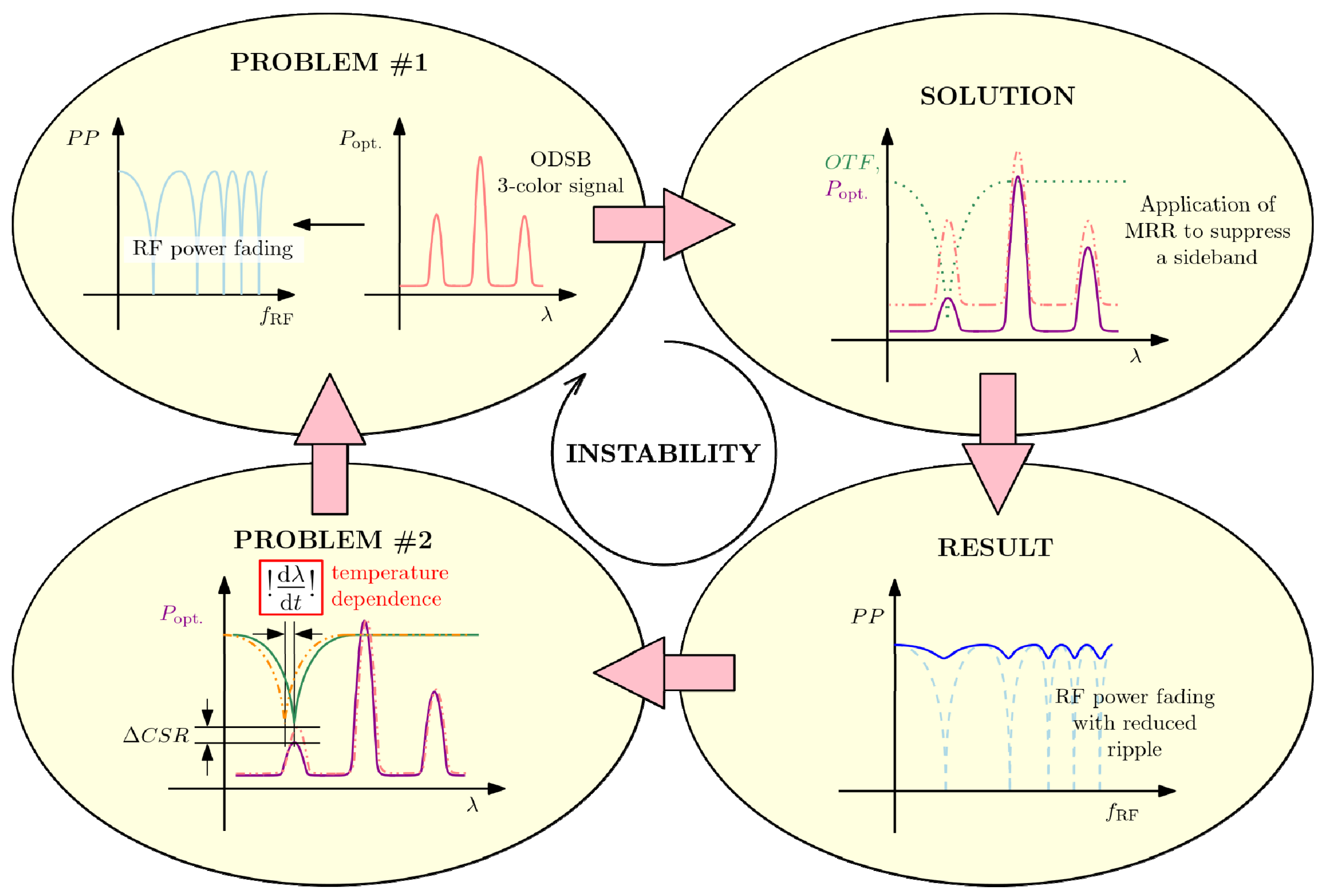
Figure 1 shows a cyclic causation diagram. The primary problem (#1) is addressed by the MRR-enabled sideband suppression, causing the undesired RF power fading to reduce to an acceptable level. Unfortunately, due to the temperature dependence of a PIC and its hosted MRR (problem #2), the solution becomes ineffective over time and the primary problem is invoked once again. We can then repeat the tuning procedure we took in the first place to realign the system, but the issue will arise again. We conclude that the system is indeed unstable due to the temperature dependence of the MRR.

2.2.2. DFB Wavelength Tuning by TEC

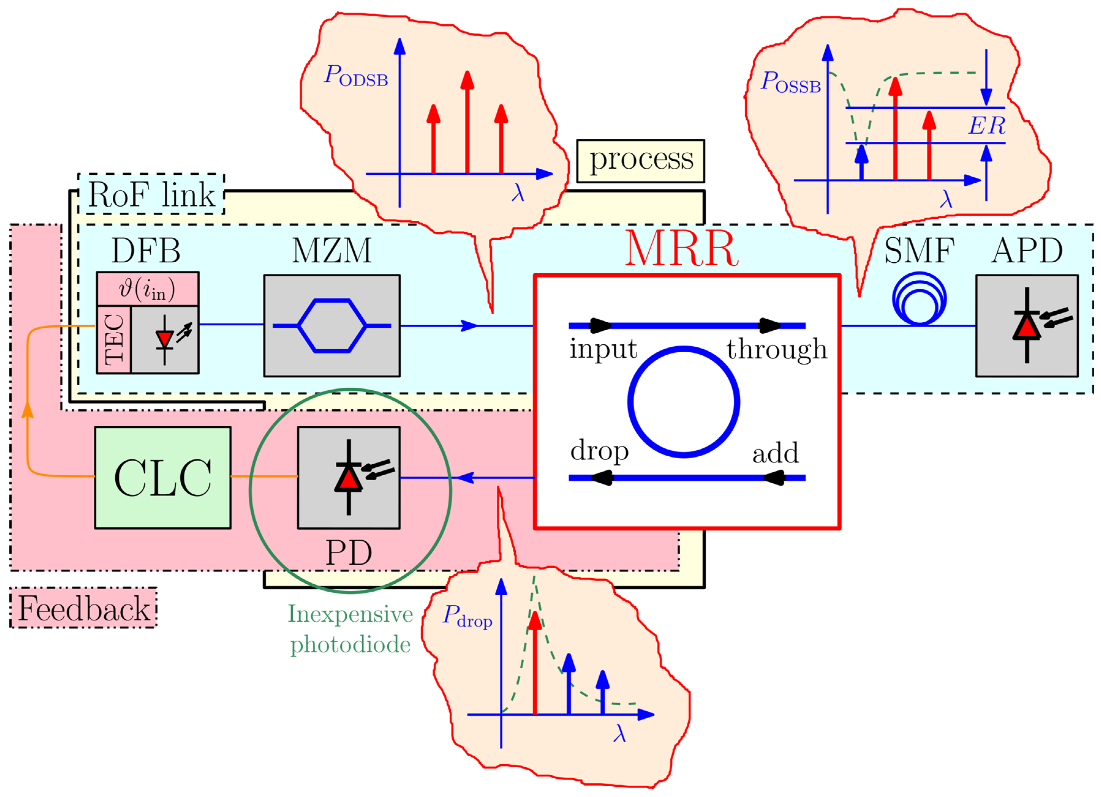
Instead of tuning the laser source and/or the MRR to a fixed absolute wavelength, we could also seek to tune one to the other, i.e., to tune a laser for its optimal (relative) alignment with one of the MRR’s resonances or vice versa. As a mechanism for tuning a DFB laser in terms of wavelength, we established an approach that involves a thermoelectric cooling (TEC) element, also known as a Peltier heat pump. This mechanism serves as the basis for all the experimental work reported in this paper. As anticipated in Figure 2, the proposed system is time dependent, thus the tuning should be continuous. This calls for a CLC system.

2.3. Closed-Loop Control (CLC)

2.3.1. Limitations and Requirements

We propose a concept that recycles the resonant energy, coupled into the otherwise unused drop port, to provide feedback to a CLC system. Namely, when the (un)desired sideband is most suppressed at the through port, most of its energy is coupled into the drop port. The task of the CLC system is to maintain the relative alignment of the laser-source’s wavelength and the MRR’s resonance such that one of the sidebands is accurately aligned with the resonance. We will now elucidate the closed-loop topology connected between the input and the drop port of the MRR, as marked by the underlying yellow polygon in 
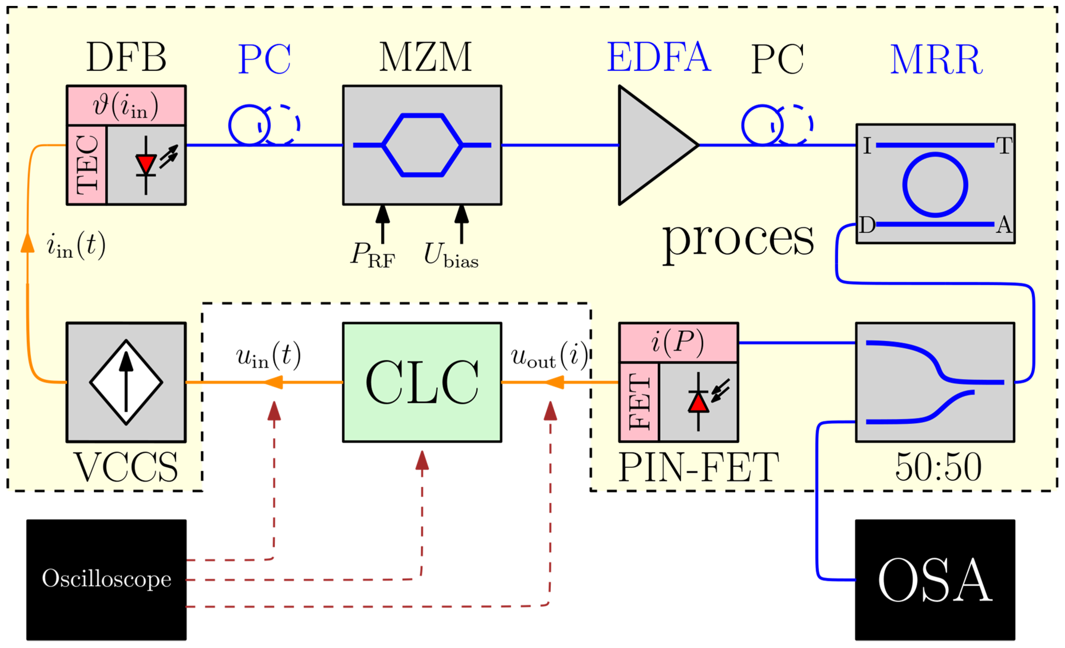
Figure 2. The blue polygon marks the part of the topology constructing the RoF link, while the pink polygon denotes the feedback topology. At the input of the MRR the signal features a typical ODSB spectral profile, whereas at the through and drop ports the signals have one of their sidebands suppressed or isolated, respectively. Note, that a real, i.e., a lossy, MRR has a finite ER, which is one of the limitations to the performance of MRR-enabled OSSB RoF links.

2.3.2. The Process

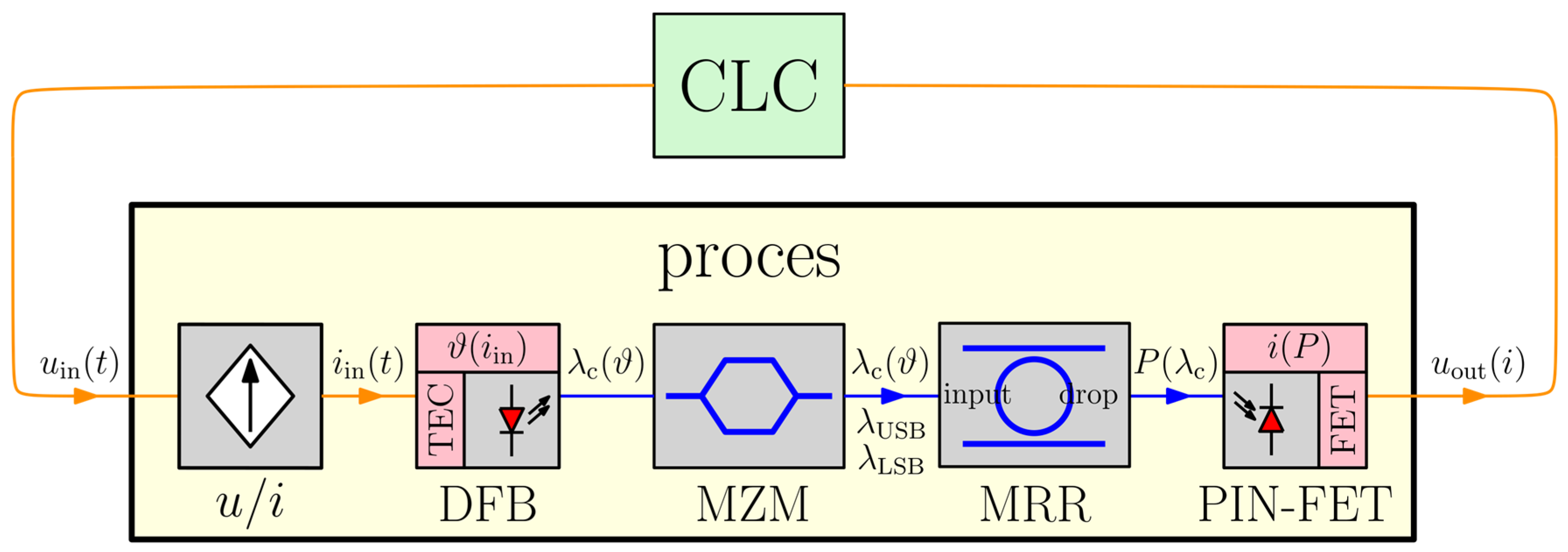
To set the ground for designing a CLC system, we must first understand the system to be tuned/controlled, i.e., the process. Figure 3 breaks down the closed-loop topology and shows the building blocks of the process.
The process begins with the voltage-controlled current source i u i n that drives the TEC elements. Its time constant should be significantly greater than that of the TEC element, which is expected to be the slowest element in the chain.
The TEC element converts the electrical current i i n (not to be confused with the laser-supply current) into heat and temperature ϑ T E C ( i i n ) change, resulting in the carrier-wavelength λ c ( ϑ T E C ) 
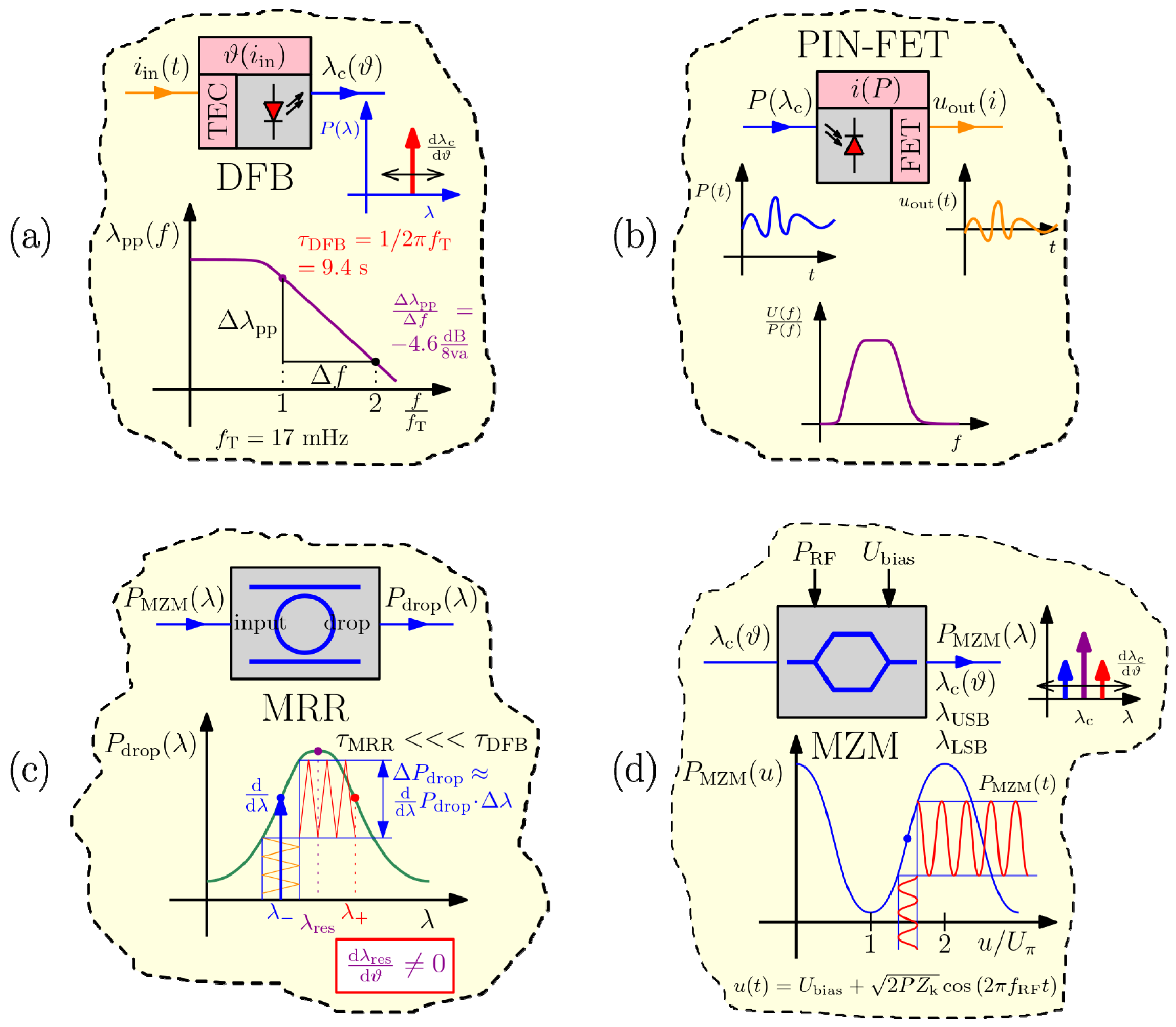
change at the laser output. The corresponding 2-port model (shown in Figure 4a) with i i n at the input and the optical power spectrum concentrated around λ c i i n at the output turns out to be a low-pass filter, featuring a 3 dB bandwidth ( B ) in the millihertz range and thus a relatively large time constant τ in the range of a few seconds. For the laser used in our experiments, these two parameters were measured at B = f C 17   m H z and τ D F B = 1 / 2 π f C 9.4   s , where f C represents the cutoff frequency. Additionally, we measured the slope ( Δ λ p p / Δ f 4.6   d B / o c t a v e ) to enable the extrapolation of the attenuation for higher modulation frequencies f . It must be noted that extrapolation can only be applied as a rough estimation, as the system is not linear. The mathematical approximation of the laser’s output power spectrum is as follows:
P D F B λ , λ c = P D F B , 0   δ [ λ λ c ]
where P D F B , 0 is the output optical power of the laser, λ is an independent variable, and λ c is a variable parameter, subject to tuning.
This carrier is subsequently modulated by the RF signal at the Mach–Zehnder modulator (MZM) (Figure 4b), which in the first approximation introduces a 3-color (higher-order harmonics are neglected, assuming the MZM is biased at the quadrature point) signal to the MRR’s input. All three resulting wavelength components are subject to temperature fluctuations λ c ϑ T E C ,   λ U S B = λ c Δ λ ,   λ L S B = λ c + Δ λ , where Δ λ λ c 2 c 0 f R F , where c 0 is the speed of light in vacuum and f R F is the RF modulation frequency. The corresponding power spectrum is:
P M Z M λ δ λ λ 0 + 1 C S R δ λ λ L S B + δ λ λ U S B ,
where C S R stands for the carrier-to-sideband ratio (CSR).
At the drop port of the MRR (Figure 4c) we obtain a modified 3-color signal P d r o p , affected by the MRR’s OTF H M R R ( λ λ r e s ) with multiple passbands spanned around the maximum transmission points at λ λ r e s k F S R ; k Z , where the observed resonance is a function of the MRR’s temperature λ r e s ( ϑ M R R ) . This temperature comes from environmental variations as well as from the self-induced heating of the system during normal operation, and is responsible for our system’s instability. Hence, the need for a CLC.
Finally, we capture the optical power spectrum at the low bandwidth PIN-FET module (Figure 4d), converting it to an electrical near direct current (DC) and voltage u o u t ( i o u t ) , while ignoring the other mixing products falling into the RF domain and beyond. Such a device basically functions as a power meter, measuring the sum of powers for all three frequency components, where the resulting voltage u o u t is proportional to the incident optical power P .
Since the time constants of the other components are several orders of magnitude smaller than those of the TEC-driven DFB laser, we can conclude that the combined time constant of the system is approximately τ p r o c e s s τ D F B .

2.3.3. Closed-Loop Control Synthesis

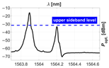
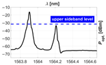
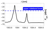
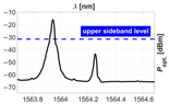
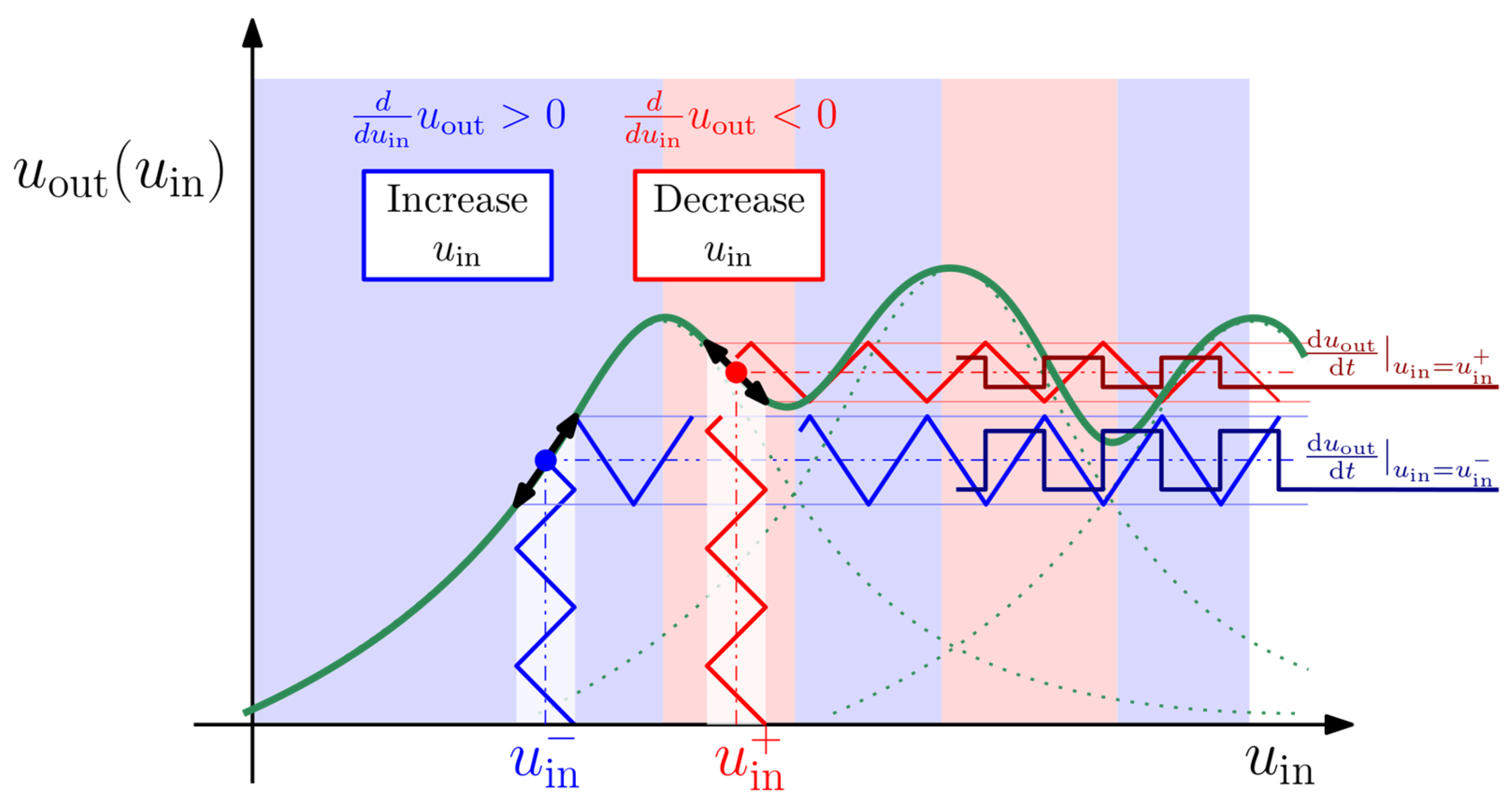
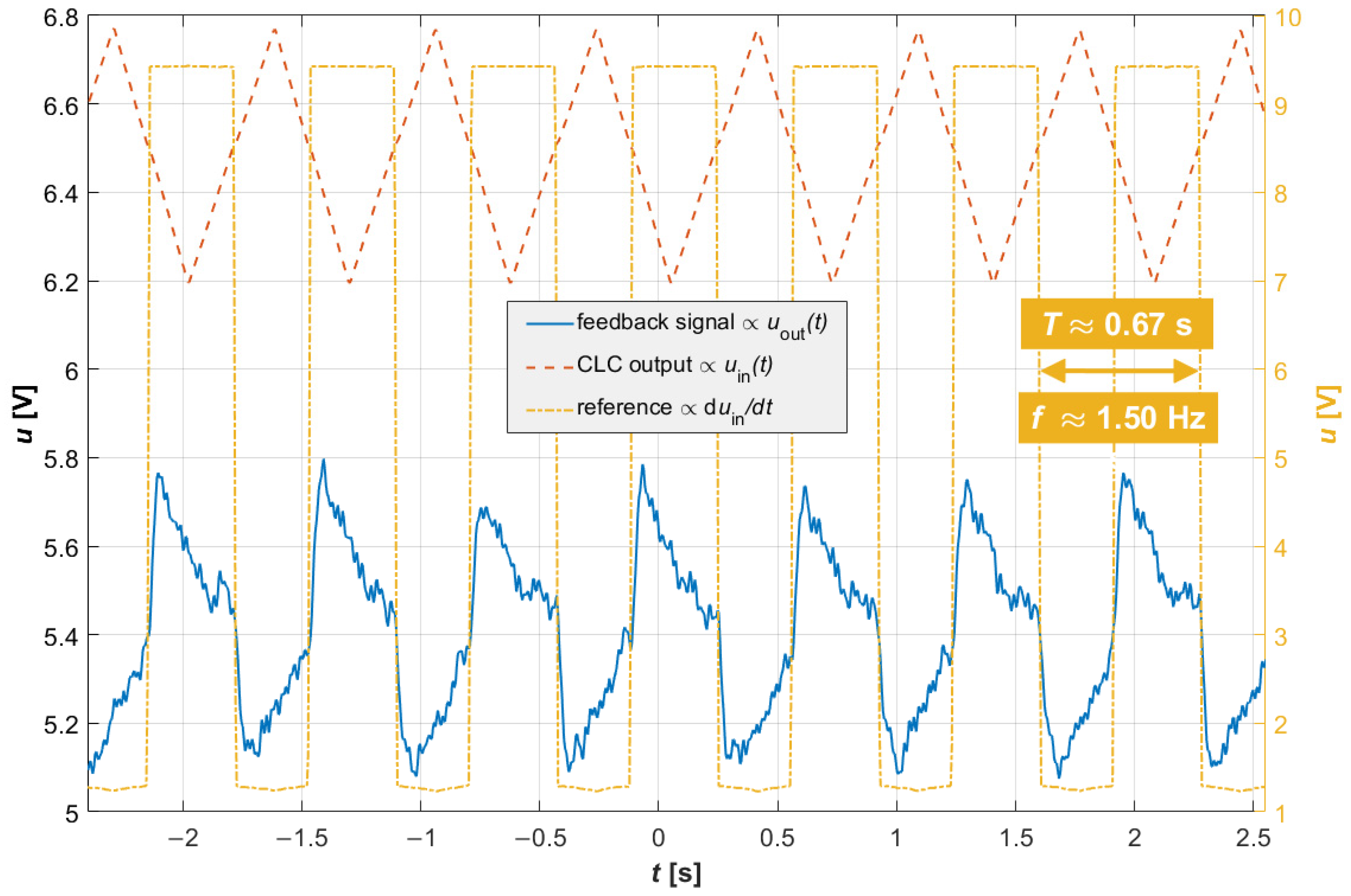
As the laser is chirped in wavelength, the photodiode measures a wavelength-dependent optical power, similar to that shown in Figure 5. The three maxima correspond to the three colors of the ODSB signal, as they pass by the MRR’s resonance. Unfortunately, the prominence of the three maxima depends on several factors, such as an MRR’s OTF and the modulation frequency (hence a shift of the sidebands from the carrier) and on a CSR. It might also be the case that the three maxima merge into one, which is unfavorable. For the CLC system to work, the maxima must be pronounced as the change in the derivative sign, which tells us whether we are on the rising d d t > 0 or falling d d t < 0 edge of a local maximum.
The input voltage signal consists of a manually set bias voltage U m a n , a slow-changing yet dynamic bias voltage from the integrator U i n t and a triangle wave voltage u ( t ) of a certain frequency and amplitude. The latter is intended for continuous sensing of the derivative sign. Given the desired near-DC behavior of U i n t , we will merge it together with U m a n into a single DC term U , which yields:
u i n t = U + u ( t )
The included DC component U sets the bias wavelength, which through the CLC system’s operation should tend towards the local maximum. To aim for one of the extreme (left or right) local maxima rather than the global maximum (in the middle), as desired, we can either set the initial bias (wavelength) point to their vicinity or involve a more advanced system that initially performs a sweep over wider range of wavelengths to locate the desired local maximum.
When any of the three spectral components approaches the MRR’s resonance, the varying wavelength is converted to amplitude variations, which are then captured by the PIN-FET photodiode and eventually converted back to an electrical (voltage) signal of similar (triangular) shape.
u o u t t = U ~ + u ~ ( t )
In principle, this is similar to the principle of slope detection from radio communications. Since the slope of the filter d P / d λ is roughly the opposite on each side of the MRR resonance, the resulting voltage signal reverses in phase as the maximum point is passed. This means that the derivatives of the input signal d u i n d t and the output signal d u o u t d t match in sign when a color approaches from the left side, and mismatch when it approaches from the right side. Both are approximately square waves. Now, if the product d u i n d t d u o u t d t is taken, we should ideally get either a positive or a negative DC voltage, which indicates whether U , and hence λ c , should be increased or decreased. The DC component U ~ is actually a measurement of the average received optical power by the photodiode and is not relevant to our CLC system’s operation, since it operates with respect to the derivative of the signal. Therefore, in the current implementation documented later on, U ~ is filtered out by the DC block capacitor of the PIN-FET module.
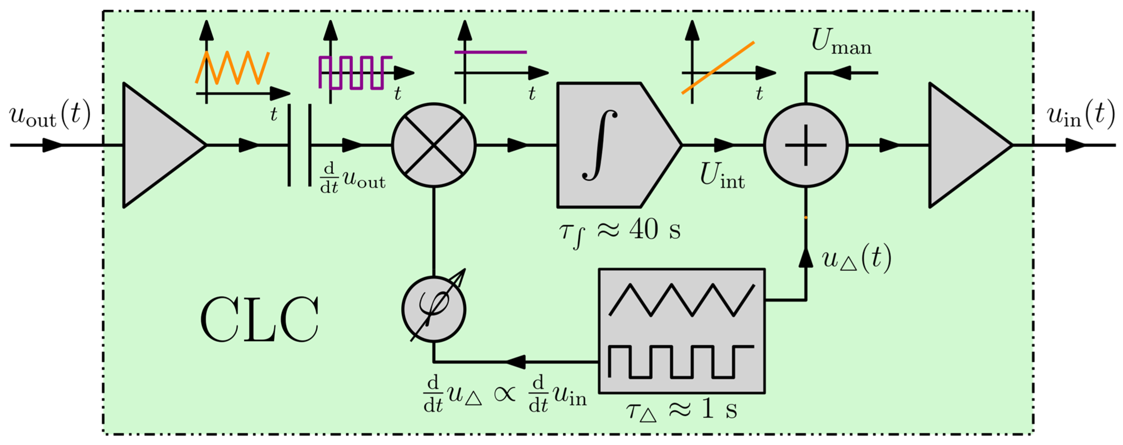
Figure 6 shows the block diagram of the proposed CLC system. Let us assume that the integrator’s output is neutral right after the startup. At this point, the signal u i n comes solely from the triangle-wave generator. As this signal from the input u i n propagates through the process, we obtain either an in-phase or out-of-phase triangle wave signal at the output u o u t . Then, the derivative is taken d u o u t d t and multiplied by the derivative of the original triangle wave d u d t . If these two are in-phase, the product is positively biased, while when out-of-phase, the product is negatively biased. This causes the integrator to chirp either up or down. In practice, there can be an additional phase shift at u o u t , which might need to be compensated by adding a relative phase shift to the reference signal d u d t . When the maximum point is reached, the product loses the DC component; therefore, the output of the integrator remains constant, as required. To determine the time constants of these building blocks we must consider the following. First, the exciting triangle wave signal should be slow enough not to be filtered out by the low-pass response of a TEC element. Therefore, we propose a time constant in a similar range, about τ 1   s . The integrator, on the other hand, should be slow enough to be filtered out by the high-pass filter at the input, i.e., τ   τ .

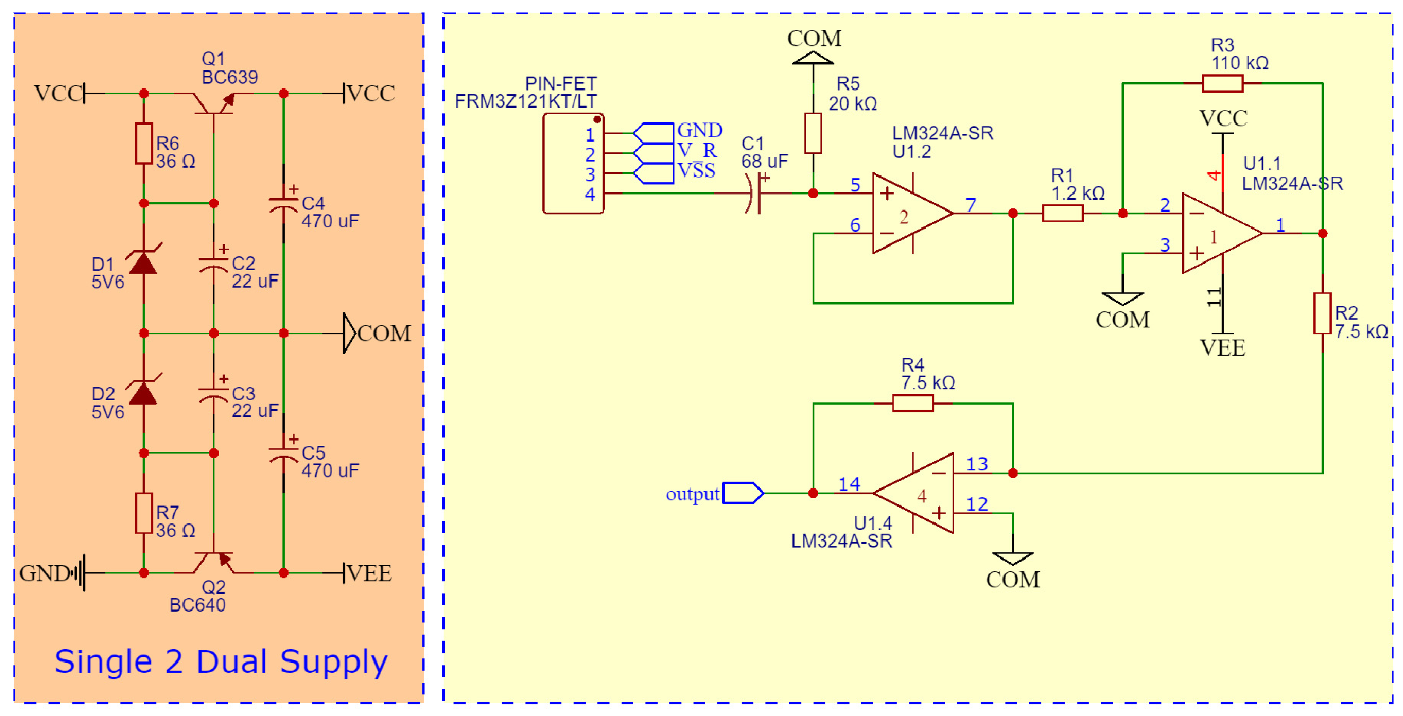
2.4. Practical Implementations

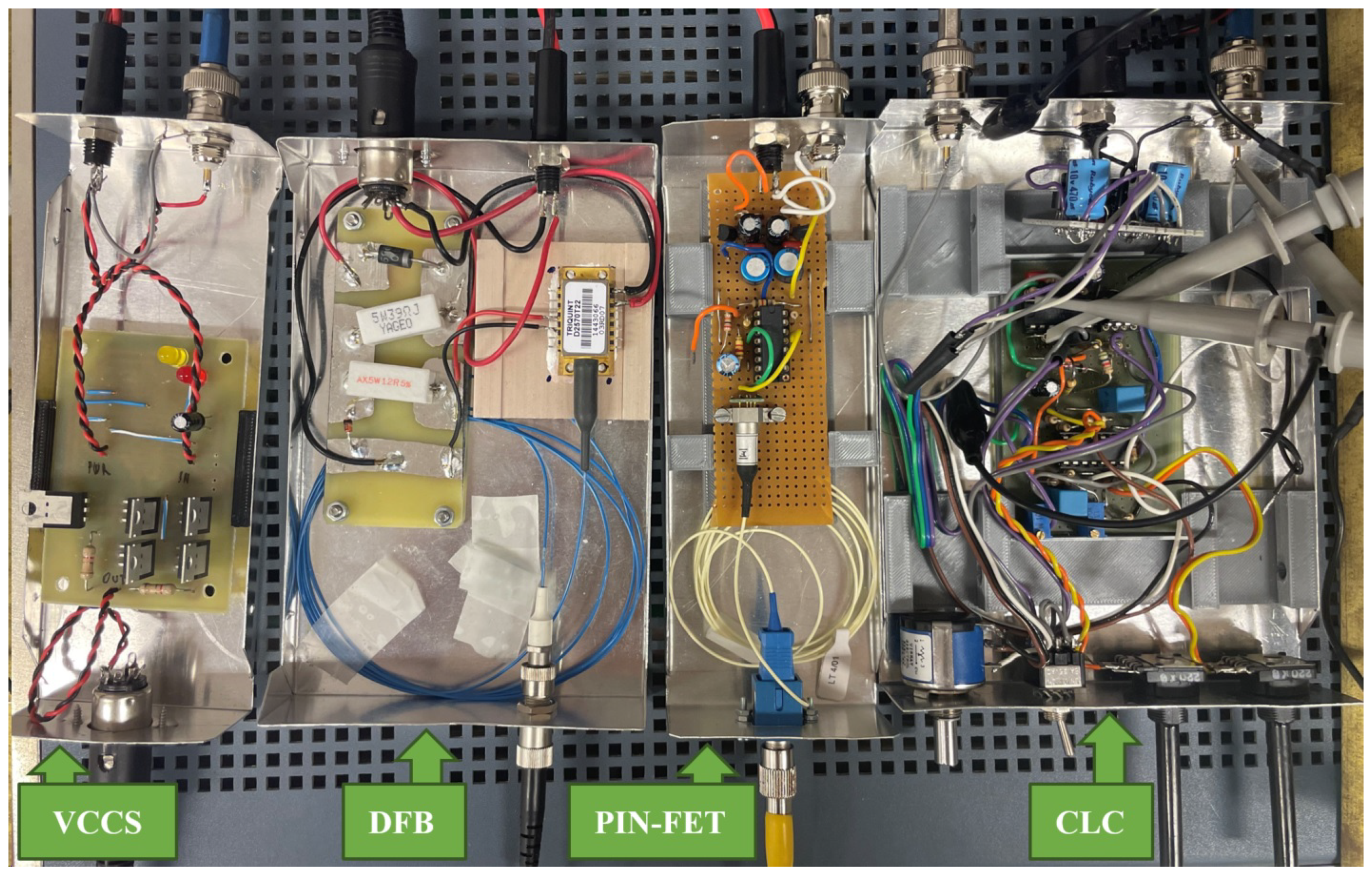
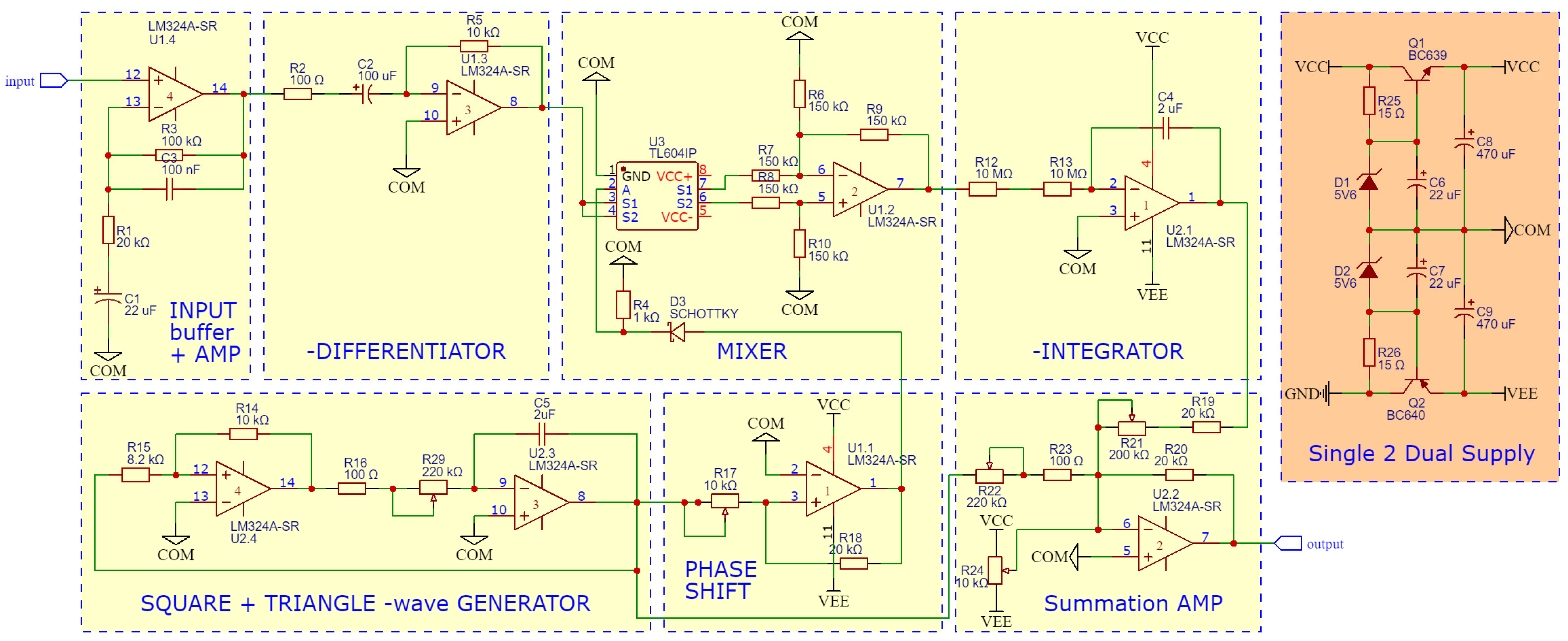
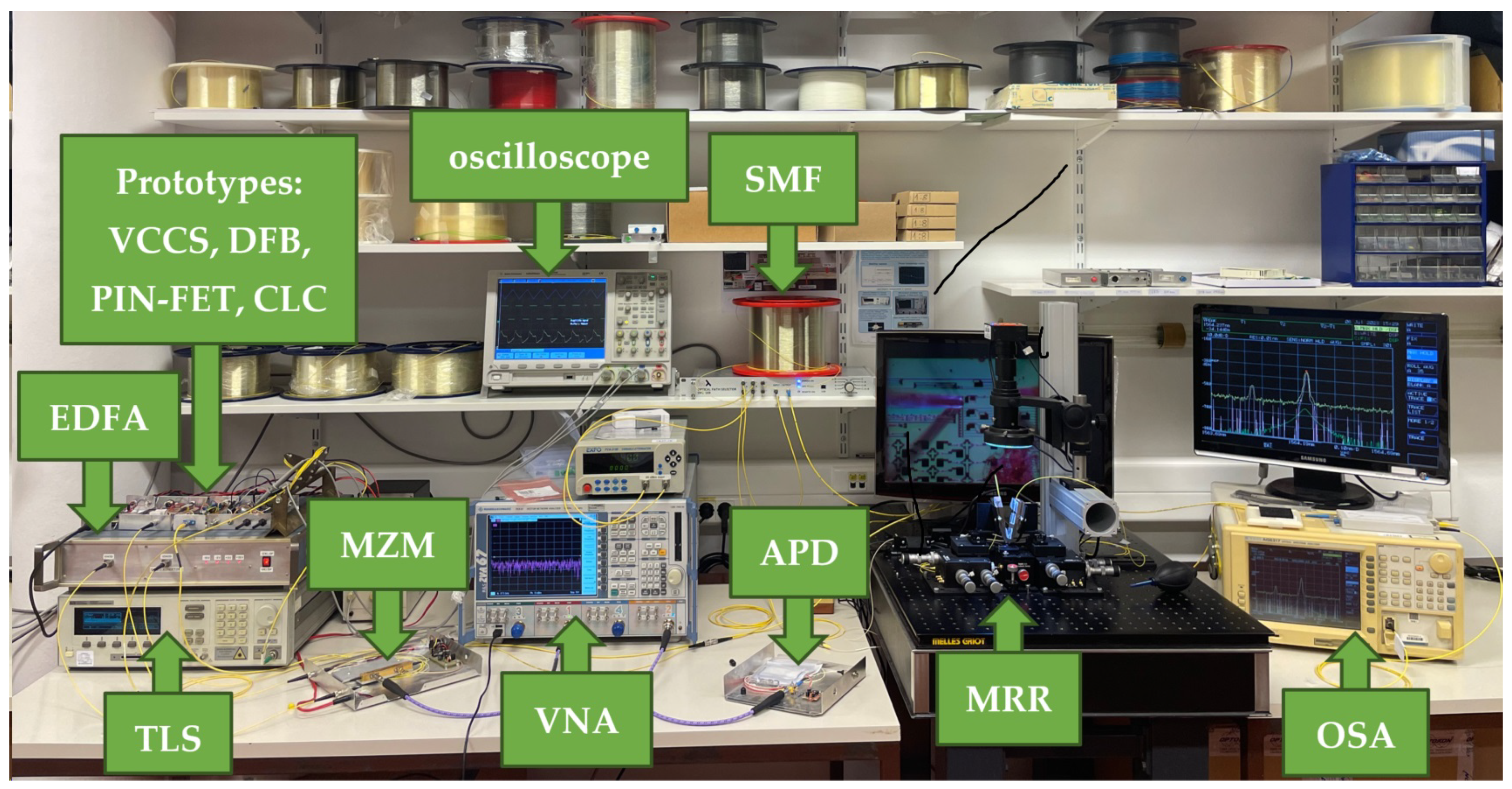
We designed and built a prototype of the CLC system to establish the environment for an experimental evaluation of the proposed concept. The CLC prototype was built from several generic operational amplifiers (LM324), a CMOS switch (TL604), and other discrete components (capacitors, resistors, potentiometers, diodes, transistors). To enable our measurements, given the low optical powers in the system, we also assembled a sensitive PIN-FET receiver, and a voltage-controlled current source (VCCS) to drive the TEC element.

2.4.1. Closed-Loop Control (CLC)

The CLC prototype was manufactured with through-hole technology elements as there are no high-frequency requirements for this part of the system. Figure 7 is a schematic with the orange block showing the power-supply adapter and the yellow block implementing the concept from the block diagram in Figure 6. The input buffer stage is designed as an active band-pass filter with approximately 14 dB of gain. The lower cut-off frequency is set to block the (near) DC term U ~ , while the upper cut-off frequency limits the bandwidth to reduce the higher-frequency noise. The mixer is built of a differential amplifier and a CMOS switch, which is triggered by a rectified square-wave voltage. So, in this case, the mixing behavior is achieved by multiplying the signal from the differentiator by −1 or 1, alternately. The square and triangle -wave generator is realized as a combination of a Schmitt-trigger circuit and an integrator op-amp circuit, where the trimmer R29 adjusts the frequency. The tunable phase shift is achieved with an additional Schmitt-trigger circuit with adjustable threshold (R17) that is triggered by a triangle-wave output from the generator. A summation amplifier combines all the signals, while letting their magnitudes be varied by means of R21, R22 and R24.

2.4.2. PIN-FET

As an inexpensive photodetector we employed a PIN-FET module FUJITSU FRM3Z121KT/LT consisting of an InGaAs PIN photodiode and a GaAs IC preamplifier. We designed an additional circuit (Figure 8) to supply it with electricity as well as to filter and further amplify the received signal. The gain is set to nearly 40 dB.

2.4.3. Voltage-Controlled Current Source (VCCS)

The VCCS was designed as a single-supply device with a reference (zero) voltage biased to 6 V, i.e., half of the 12 V supply voltage. This is an H-bridge circuit with additional current-control circuitry. The voltage-to-current conversion slope was measured at approximately i i n / u i n 86   m A / V .
Figure 9 shows the laboratory-built prototypes that were synthesized, designed, and manufactured to accommodate the experimental evaluation of the proposed concept. In the photograph, viewed from left to right, these are the VCCS, the DFB module, the PIN-FET module, and the CLC prototype.

3. Evaluation and Results

3.1. Evaluation Metrics

The evaluation is carried out in two consecutive steps, i.e., Step 1 and Step 2, with an appropriate variation of the experimental setup. The two setups will, from this point onwards, be referred to as setups Variant 1 and Variant 2.

3.1.1. Step 1: Optical Wavelength Dither

First, we will show that the system can be successfully stabilized, i.e., the sideband wavelength can be locked to the MRR’s resonant wavelength with a residual wavelength misalignment Δ λ = λ x S B λ r e s ε λ , constrained by the limits of ± ε λ . The parameter ε λ depends on the configuration of the CLC, i.e., the amplitude and the frequency of the triangle-wave excitation, and it cannot be expected to vanish completely. The objective of this first step is to optimize the parameters of the CLC for the minimal dither, while still maintaining the locked state, and to measure its value ε λ . The corresponding experimental setup variant will be referred to as Variant 1.

3.1.2. Step 2: RF Power Penalty

In the second step, we evaluate the performance of the RoF link with the inherent power fading mitigated by means of a single integrated add/drop MRR while considering the above dither. In particular, we will measure the PP function for several misalignments Δ λ within the range governed by the dither ε λ . Finally, we will present the deterioration of the PP at a specific frequency f 0 as a function of misalignment Δ λ :
Δ P P f 0 , Δ λ d B = P P f 0 , 0 d B P P f 0 , Δ λ [ d B ]
The frequency f 0 corresponds to the first extreme value (dip) in the PP function for the RoF link under consideration when uncompensated. This depends on the fiber-dispersion properties, the fiber length, and the carrier wavelength. Concrete values will be presented further on. The corresponding experimental setup variant is referred to as Variant 2.

3.2. Experimental Setup

All the experiments were carried out in a laboratory environment. The sensitive optical components such as the MRR and the coupling fiber pigtails were suspended on a mechanically isolated optical table. The MRR was coupled through vertical coupling with the SMF pigtails. Optical polarization controllers were included in the setup to optimize the performance of polarization-sensitive devices such as the MZM and MRR. Since polarization-dependent grating couplers were used as the couplers between the PIC and the optical fibers, which can only effectively couple TE polarized light, the polarization needs to be precisely tuned for efficient coupling. To eliminate the need to tune the polarization, we can rely on polarization-maintaining fibers, employ a polarization-diversity approach [42] or use a polarization-insensitive MRR [43].

3.2.1. Setup: Variant 1

Variant 1 contains the setup from Figure 3 with some additional measurement and miscellaneous equipment to enable the evaluation. In the electrical part, we used an oscilloscope to perform time-domain measurements at several points to confirm the intended behavior of our prototyped components. In the optical part we coupled out half of the optical power just after the MRR drop port to observe the wavelength spectrum in real time with an optical spectrum analyzer (OSA). This enabled us to measure the wavelength dither.
Figure 10 shows a block diagram of setup Variant 1 with the following components, viewed from left to right: A VCCS, a heat-pump-controlled DFB laser (tunable between 1563.5 and 1565.5 nm), an optical polarization controller (PC), a MZM, an erbium-doped fiber amplifier (EDFA), another PC, a PIC with the MRR under consideration coupled to the input and the drop port, a 50:50 optical coupler of which one output is connected to the OSA and the other to a PIN-FET receiver, and finally a CLC system whose output is connected back to the input of the VCCS. A tunable RF modulation frequency is provided by the VNA.

3.2.2. Setup: Variant 2

This variation is customized for high-resolution (and thus slow) measurements of the optical spectrum using the OSA and the radio-frequency spectrum using a vector network analyzer (VNA). We replaced the DFB laser with a tunable laser source (TLS), featuring a resolution of 0.001 nm (~123 MHz), to enable accurate adjustment of the wavelength. The CLC system is excluded from this setup, as we are looking into the effect of the wavelength dither for several discrete points, one at the time. We will refer to these as misalignments of the carrier wavelength and the MRRs resonance. A photodiode terminating the RoF link is a high-performance avalanche photodiode (APD) with a bandwidth exceeding 40 GHz.
Figure 11 shows a block diagram of setup Variant 2 including the following components starting from the left: a TLS, an optical polarization controller (PC), a MZM, an EDFA, another PC, an MRR on a PIC, a 2.512   k m SMF, a 50:50 fiber coupler to provide an optical signal to both the OSA and the APD terminated by a VNA.
The particular length of the fiber is chosen in such a way that the first dip in the power-penalty function is encountered, given the intended mmW frequency f 0 . This should demonstrate that even at relatively short distances the chromatic-dispersion-related effects might need to be considered and addressed.
In Figure 12 there is a photograph of our experimental environment in the laboratory, accommodating both of the above-depicted setup variations.

3.3. Results

In this subsection, we present the results acquired using the methods presented in the previous subsections. Before revealing the main results evaluating the performance of the wavelength-locking system, we will quantitatively present certain important parameters of our setup and the corresponding building blocks.
We used the MRR6 from the same PIC that accommodates the previously investigated MRR3. MRR6 features a FSR of 3.40 nm (~417 GHz), an in-through extinction ratio of E R i n t h r o u g h = 6.84   d B , a FWHMs or bandwidths of B i n t h r o u g h = 0.085   n m (~10.4 GHz) and B i n d r o p = 0.1234   n m (~15.1 GHz) in the in-through and in-drop OTFs, respectively. With its in-drop extinction ratio E R i n d r o p exceeding 20   d B , the MRR6 proved suitable for the wavelength-locking application. The OTFs when terminated at the through port (red line), and when terminated at the drop port (purple line), are presented in Figure 13.
The exact wavelength of sidebands is determined by both the carrier wavelength and the mmW modulation-frequency setting. Given the properties of MRR6, the targeted mmW frequency of around 39 GHz and the DFB laser’s tuning range, we chose a carrier wavelength of λ c = 1563.97   n m (~191.820 THz) and mmW frequency f 0 = 37.8   G H z . These two parameters are relevant to all the measurement results presented later on.

3.3.1. Optical Wavelength Dither

To evaluate the wavelength dither, we first manually adjusted the CLC system to roughly align the sideband with the MRR resonant peak. Next, we let our CLC system lock the wavelength more precisely, while adjusting the frequency and amplitude of the modulation signal for the minimum working dither. Note that the optical power of the sideband is greater than that of the carrier, which can be seen on its left. Whether this actually happens or not depends on several factors, such as the RF gain of the MZM (also dependent on its bias setting), the ER of the MRR, the polarization control, etc. However, this is a requirement for the system to work as otherwise the system would tend to align the carrier—rather than the sideband—with the MRR’s resonance. After meeting this requirement, we performed three measurements, which we show graphically in Figure 14 below. We captured the instantaneous optical spectrum (red solid line) and, given the time constant of our CLC system, we performed a max-hold optical spectrum measurement with a duration of T = 300   s τ   (blue dash-dotted line)—significantly longer than that of the integrator in the CLC system. To confirm the alignment with the MRR’s resonance, we also captured the input-drop MRR OTF and included it in the same graph (orange dashed line). The resulting dither was evaluated at ε λ = B b l u e B o r a n g e / 2 0.0038   n m (~466 GHz).
The resonant wavelength in Figure 13 differs from that in Figure 14. This is because before the latter measurement was performed the system had been running for some time (and therefore resonance shifting) to confirm the successful long-term locking.
The locking state was achieved and the measurements performed with the CLC set to a frequency of f 1.5   H z , as can also be seen from the Figure 15. This figure shows the oscillogram with voltage measurements at several points of the CLC circuit. The red dashed line presents the voltage signal u i n controlling the VCCS, the orange dash-dotted line shows the rectangular signal with the phase corrected and fed to the input of the mixer, and finally the blue solid line presents the signal measured after the buffer amplifier at the input of the CLC. This last is actually the feedback signal that is essential for our concept of wavelength locking.

3.3.2. RF Power Penalty

First, we measured the optical powers at several (marked) points A–E (Figure 11) along the path of the optical signal propagation and present them together with the RF power setting at the output (point Z) of the VNA in Table 1.
The careful reader will notice the excessive drop in the optical power after the MZM (point B). This is due to the lower-than-typical bias voltage that was employed to achieve the small-enough CSR for the wavelength locking to have worked.
To determine the performance of the RoF link, we examined the optical power spectrum of an OSSB signal with a varying SBSR and the RF transfer functions (TF), i.e., the s 21 measurement, for several (mis)alignments of the carrier wavelength Δ λ = ± n δ λ with a discrete step of δ λ = 0.01 and n = 0 ,   1 ,   2 ,   3 10 . Note that when the carrier wavelength is misaligned, the SBSR deteriorates and the PP at the intended RF, visible on the TF, intensifies.
In the Table 2, we show pairs of graphs—referring to the optical power spectrum of the transmitted OSSB signal and the corresponding RF TF of the RoF link shown in Figure 11—for the first five misalignments from the optimal to shorter wavelengths.
The following graph (Figure 16a) combines all the RF TF measurements for the red-shifted and blue-shifted wavelengths. If we now acquire the values at a critical frequency f 0 , where without the MRR there would have been an extreme power penalty P P f 0   d B , we obtain the following graph (Figure 16b). It relates the PP deterioration to the wavelength misalignment. Given the dither evaluated at ε λ 0.0038   n m < 0.01   n m , we can conclude that Δ P P f 0 , Δ λ Δ λ < ε λ < 2   d B .

4. Discussion

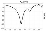
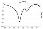
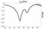
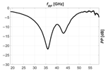
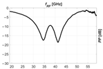
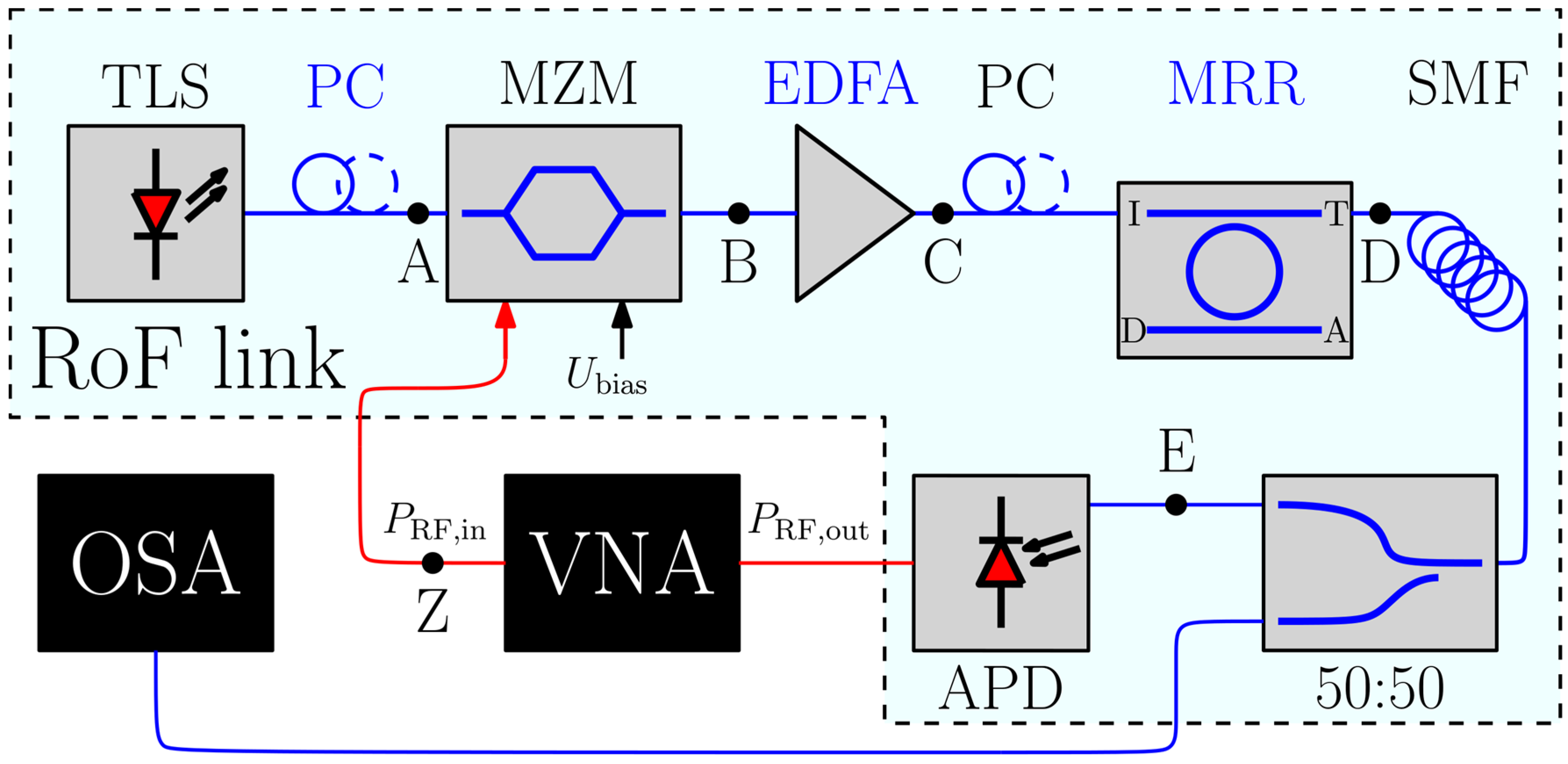
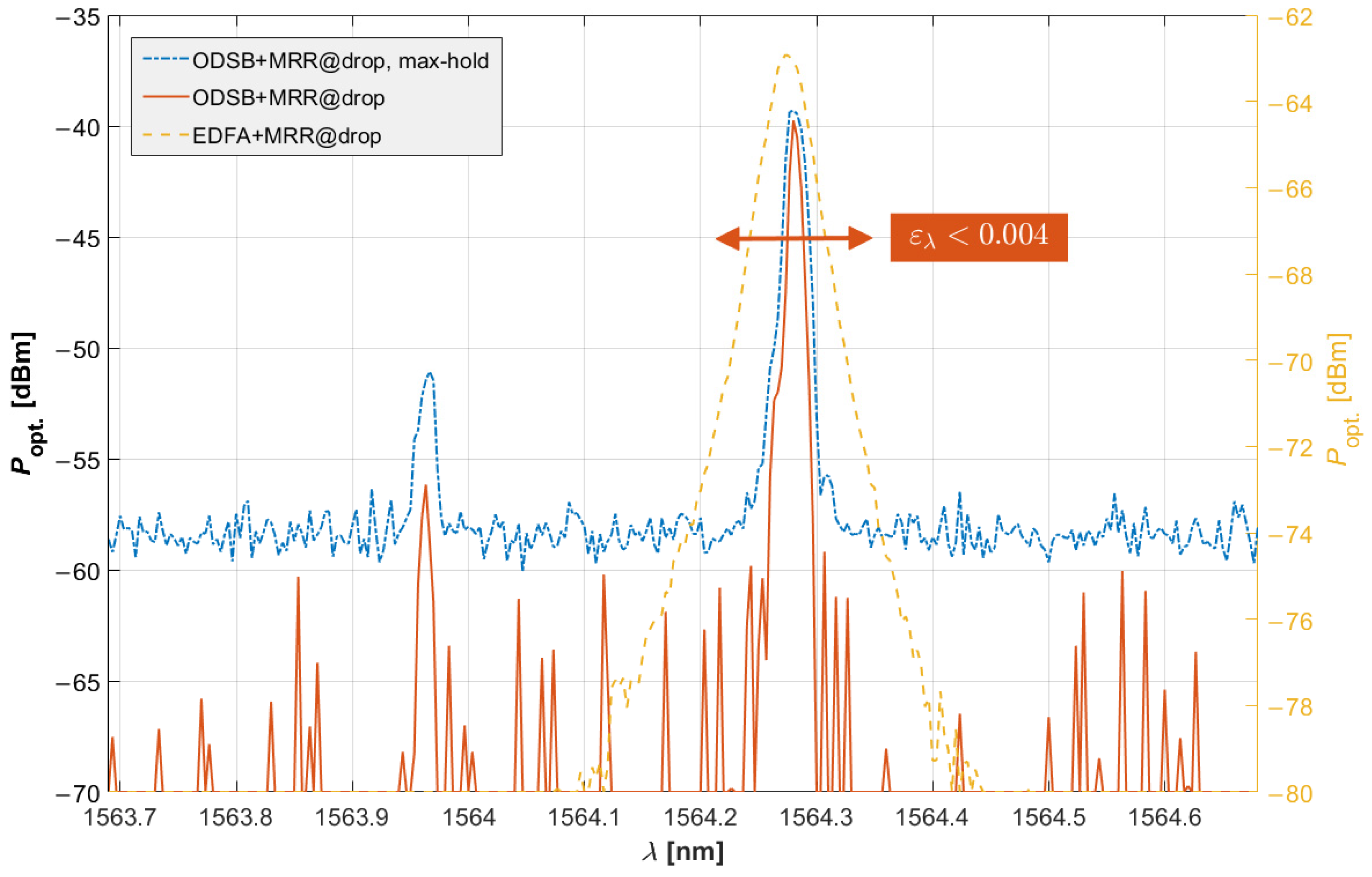
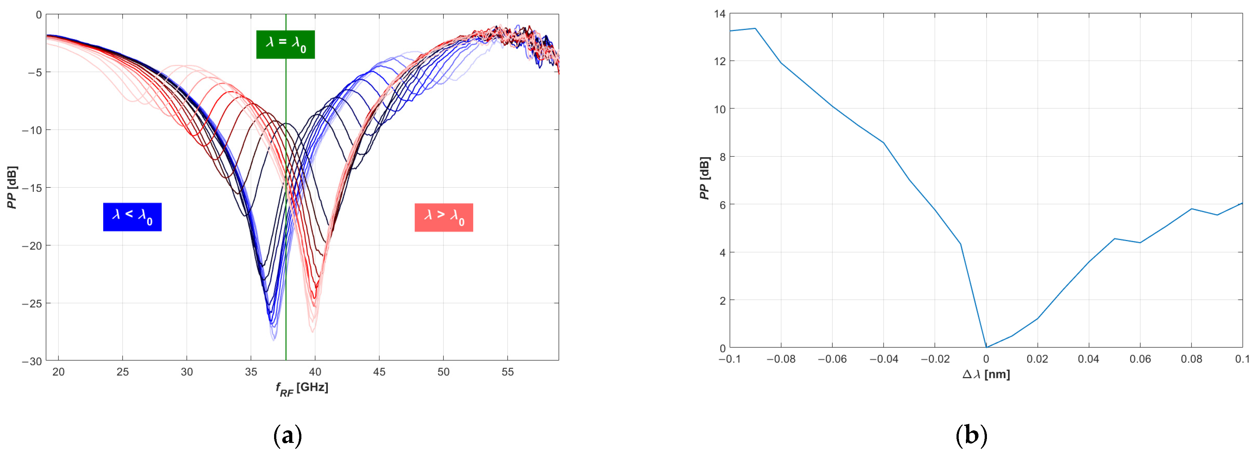
In this section, we discuss in detail the presented measurements and the results of the study, which addresses the novel approach of using an MRR and a heat-pump-controlled laser to achieve analog wavelength locking in mmW RoF links. This approach offers a potential solution to mitigate the wavelength-drift issues causing the PP deterioration, which is critical to maintaining the signal integrity in communication systems. Experimental validation of the effectiveness of the MRR in wavelength locking is a notable contribution of the work, representing an advance over conventional wavelength-stabilization techniques.
In our experimental work (Step 1), we have shown that the carrier wavelength and the selected MRR resonance can be successfully interlocked using a purely analog CLC system in conjunction with a heat-pump-controlled DFB laser. While this challenge has been well addressed by a number of researchers, as presented in the introduction of this paper, our concept is the first to approach the challenge by employing the integrated Peltier heat pump of an ordinary DFB laser module in a so-called butterfly package. Advantageously, our approach removes the need for complex photonic structures with enabled thermal management. It also allows for direct relative wavelength interlocking and is immune not only to the MRR’s temperature instability but also to that of the laser. The locking mechanism involves a (triangle-wave) modulation (in the referenced papers also referred to as dithering) signal causing an unavoidable, yet minimizable and acceptable wavelength dither. The latter is also inherent to and considered in some solutions by other researchers. The experimental setup we developed enabled us to effectively interlock the wavelengths while minimizing the dither to less than 0.004 nm (~491 MHz). Among other building blocks, this result depends on the characteristics of the MRR. The latter also influence the extent of the PF mitigation by its extinction ratio in the input-through direction. Accordingly, as clear from Figure 16, the PP function does not reach zero even at the target frequency f 0 . Though this alone does not obstruct our wavelength-locking concept, as the performance of the locking is determined by the wavelength dither and the resulting PP deterioration (measured at < 2   d B ), rather than by the absolute PP number at f 0 . Excessive dither amplitude might also increase the unwanted behavior, where the CLC system hops between the states with either the sidebands or the carrier being aligned with the MRR’s resonance. Some key performance parameters of our wavelength locking system are summarized in the Table 3 and compared to a few referenced solutions.
However, from a more general perspective these potential disadvantages could be lessened by carefully choosing or even designing a purposeful MRR when aiming at a high-performance end-product development and manufacturing. The next steps in this research should be lowering the time constant of the process and thereby allowing for a faster-responding CLC and determining the criterion for a suitable MRR resonator for this task.

5. Conclusions

This paper addressed the challenge of an SOI MRR’s temperature dependence, compromising the performance of an MRR-enabled mmW OSSB RoF transmitter. The varying ambient or in-system-induced temperature changes the relative alignment of the laser (carrier) and the MRR’s resonant wavelengths. Therefore, we identified the need for a closed-loop control system to stabilize the transmitter by means of wavelength interlocking. We presented the underlying theory and proposed a concept for the CLC system. Based on this concept, we designed and manufactured several prototype devices constructing or assisting the CLC system. We established the experimental setup to quantitatively evaluate the performance of the proposed system. Using our CLC system, we successfully locked the carrier wavelength of the TEC-driven DFB laser with an unavoidable wavelength dither of less than 0.004   n m (~491 MHz). Considering the latter and the parameters of our system (such as fiber length, RF-modulation frequency range, and MRR characteristics) we managed to keep the power-penalty deterioration under 2 dB. While this paper focused on proving the stabilization concept, it should be noted that for a dedicated application the MRR might need to be carefully selected or designed, given the actual parameters of the RoF link under consideration (i.e., intended channel bandwidth, required link budget, etc.). Therefore, we expect that a purposefully designed MRR should offer better performance, which should be investigated in future research.

Author Contributions

Conceptualization, K.V.B. and M.V.; methodology, K.V.B.; software, K.V.B.; validation, B.B., A.D. and K.V.B.; formal analysis, K.V.B.; investigation, K.V.B. and A.D.; resources, B.B. and A.D.; data curation, K.V.B.; writing—original draft preparation, K.V.B. and A.D.; writing—review and editing, B.B. and A.D.; visualization, K.V.B.; supervision, B.B.; project administration, K.V.B., A.D. and B.B.; funding acquisition, B.B. All authors have read and agreed to the published version of the manuscript.

Funding

This work was supported by the Slovenian Research and Innovation Agency under grants J2-3048, J2-50072 and research core funds P2-0415 and P2-0246.

Institutional Review Board Statement

Not applicable.

Informed Consent Statement

Not applicable.

Data Availability Statement

Data are contained within the article.

Acknowledgments

We thank W. Bogaerts from Photonics Research Group of Ghent University for providing silicon PICs with MRRs.

Conflicts of Interest

The authors declare no conflict of interest. The funders had no role in the design of the study; in the collection, analyses, or interpretation of data; in the writing of the manuscript; or in the decision to publish the results.

References

  1. Batagelj, B.; Capmany, J.; Udvary, E.G. 5th-Generation Mobile Access Networks Assisted by Integrated Microwave Photonics. In Proceedings of the 2019 International Workshop on Fiber Optics in Access Networks (FOAN), Sarajevo, Bosnia and Herzegovina, 2–4 September 2019; pp. 1–6. [Google Scholar]
  2. Hilt, A. Throughput Estimation of K-zone Gbps Radio Links Operating in the E-band. Inf. Midem 2022, 52, 29–39. [Google Scholar]
  3. Rappaport, T.S.; MacCartney, G.R.; Samimi, M.K.; Sun, S. Wideband Millimeter-Wave Propagation Measurements and Channel Models for Future Wireless Communication System Design. IEEE Trans. Commun. 2015, 63, 3029–3056. [Google Scholar] [CrossRef]
  4. Asha, D.S. A comprehensive review of Millimeterwave based radio over fiber for 5G front haul transmissions. Indian J. Sci. Technol. 2021, 14, 86–100. [Google Scholar]
  5. Beas, J.; Castanon, G.; Aldaya, I.; Aragón-Zavala, A.; Campuzano, G. Millimeter-Wave Frequency Radio over Fiber Systems: A Survey. IEEE Commun. Surv. Tutor. 2013, 15, 1593–1619. [Google Scholar] [CrossRef]
  6. Ilgaz, M.A.; Vuk Baliž, K.; Batagelj, B. A flexible approach to combating chromatic dispersion in a centralized 5G network. Opto-Electron. Rev. 2023, 28, 35–42. [Google Scholar]
  7. Kasthuri, P.; Prakash, P.; Madhan, M.G. Performance Analysis of Dispersion Compensation Schemes with Delay Line Filter. Inf. Midem 2020, 50, 285–292. [Google Scholar]
  8. Zakrzewski, Z. Optical Channel Selection Avoiding DIPP in DSB-RFoF Fronthaul Interface. Entropy 2021, 23, 1554. [Google Scholar] [CrossRef]
  9. Loayssa, A.; Benito, D.; Garde, M. Single-sideband suppressed-carrier modulation using a single-electrode electrooptic modulator. IEEE Photon.-Technol. Lett. 2001, 13, 869–871. [Google Scholar] [CrossRef]
  10. Smith, G.; Novak, D.; Ahmed, Z. Overcoming chromatic-dispersion effects in fiber-wireless systems incorporating external modulators. IEEE Trans. Microw. Theory Tech. 1997, 45, 1410–1415. [Google Scholar] [CrossRef]
  11. Sampath, K.I.A.; Takano, K.; Maeda, J. Peak-to-Average Power Ratio Reduction of Carrier-Suppressed Optical SSB Modulation: Performance Comparison of Three Methods. Photonics 2021, 8, 67. [Google Scholar] [CrossRef]
  12. Middleton, C.; DeSalvo, R. High performance microwave photonic links using double sideband suppressed carrier modulation and balanced coherent heterodyne detection. In Proceedings of the MILCOM 2009–2009 IEEE Military Communications Conference, Boston, MA, USA, 18–21 October 2009; pp. 1–6. [Google Scholar]
  13. Zhu, Z.; Zheng, X.; Xu, G.; Guo, Y.; Zhang, H. A Super-Tripling Technology Used in Radio-Over-Fiber Systems for Multiservice Wireless Signals within a Millimeter-Wave Band. IEEE Photon.-Technol. Lett. 2009, 21, 1520–1522. [Google Scholar] [CrossRef]
  14. Wang, X.; Liu, Z.; Wang, S.; Sun, D.; Dong, Y.; Hu, W. Photonic radio-frequency dissemination via optical fiber with high-phase stability. Opt. Lett. 2015, 40, 2618–2621. [Google Scholar] [CrossRef] [PubMed]
  15. Nikas, T.; Bogris, A.; Syvridis, D. Double sideband suppressed carrier modulation for stable fiber delivery of radio frequency standards. Opt. Commun. 2017, 382, 182–185. [Google Scholar] [CrossRef]
  16. Bogaerts, W.; De Heyn, P.; Van Vaerenbergh, T.; De Vos, K.; Selvaraja, S.K.; Claes, T.; Dumon, P.; Bienstman, P.; Van Thourhout, D.; Baets, R. Silicon microring resonators. Laser Photonics Rev. 2012, 6, 47–73. [Google Scholar] [CrossRef]
  17. Vuk Baliž, K.; Debevc, A.; Krč, J.; Batagelj, B. Power-fading-mitigation approach in an intensity-modulated radio-over-fiber link using a single integrated micro-ring resonator. Opt. Fiber Technol. 2022, 73, 103008. [Google Scholar] [CrossRef]
  18. Chew, S.X.; Yi, X.; Song, S.; Li, L.; Bian, P.; Nguyen, L.; Minasian, R.A. Silicon-on-Insulator Dual-Ring Notch Filter for Optical Sideband Suppression and Spectral Characterization. J. Light. Technol. 2016, 34, 4705–4714. [Google Scholar] [CrossRef]
  19. Pandey, A.; Selvaraja, S.K. Broadly tunable wideband optical single sideband generation using self-coupled silicon resonator. Opt. Express 2019, 27, 8476–8487. [Google Scholar] [CrossRef]
  20. Cheng, W.; Lin, D.; Wang, P.; Shi, S.; Lu, M.; Wang, J.; Guo, C.; Chen, Y.; Cang, Z.; Tian, Z.; et al. Tunable bandpass microwave photonic filter with largely reconfigurable bandwidth and steep shape factor based on cascaded silicon nitride micro-ring resonators. Opt. Express 2023, 31, 25648–25661. [Google Scholar] [CrossRef]
  21. Teng, J.; Dumon, P.; Bogaerts, W.; Zhang, H.; Jian, X.; Han, X.; Zhao, M.; Morthier, G.; Baets, R. Athermal Silicon-on-insulator ring resonators by overlaying a polymer cladding on narrowed waveguides. Opt. Express 2009, 17, 14627–14633. [Google Scholar] [CrossRef]
  22. Padmaraju, K.; Bergman, K. Resolving the thermal challenges for silicon microring resonator devices. Nanophotonics 2014, 3, 269–281. [Google Scholar] [CrossRef]
  23. Cao, H.; Li, H.; Dai, D. Ultra-high-efficiency tunable silicon photonic filter. In Proceedings of the SPIE-CLP Conference on Advanced Photonics 2022, Hangzhou, China, 21–23 November 2022; pp. 80–83. [Google Scholar]
  24. Pintus, P.; Hofbauer, M.; Manganelli, C.L.; Fournier, M.; Gundavarapu, S.; Lemonnier, O.; Gambini, F.; Adelmini, L.; Meinhart, C.; Kopp, C.; et al. PWM-Driven Thermally Tunable Silicon Microring Resonators: Design, Fabrication, and Characterization. Laser Photonics Rev. 2019, 13, 1800275. [Google Scholar] [CrossRef]
  25. DeRose, C.T.; Watts, M.R.; Trotter, D.C.; Luck, D.L.; Nielson, G.N.; Young, R.W. Silicon microring modulator with integrated heater and temperature sensor for thermal control. In Proceedings of the Conference on Lasers and Electro-Optics, San Jose, CA, USA, 16–21 May 2010; p. CThJ3. [Google Scholar]
  26. Padmaraju, K.; Logan, D.F.; Zhu, X.; Ackert, J.J.; Knights, A.P.; Bergman, K. Integrated thermal stabilization of a microring modulator. Opt. Express 2013, 21, 14342–14350. [Google Scholar] [CrossRef] [PubMed]
  27. Padmaraju, K.; Logan, D.; Bergman, K.; Ackert, J.; Knights, A. Wavelength locking of microring resonators and modulators using a dithering signal. In Proceedings of the 39th European Conference and Exhibition on Optical Communication (ECOC 2013), London, UK, 22–26 September 2013. [Google Scholar]
  28. Jayatilleka, H.; Murray, K.; Guille, M.A.; Caverley, M.; Hu, R.; Jaeger, N.A.F.; Chrostowski, L.; Shekhar, S. Wavelength tuning and stabilization of microring-based filters using silicon in-resonator photoconductive heaters. Opt. Express 2015, 23, 25084–25097. [Google Scholar] [CrossRef] [PubMed]
  29. Agarwal, S.; Ingels, M.; Pantouvaki, M.; Steyaert, M.; Absil, P.; Van Campenhout, J. Wavelength Locking of a Si Ring Modulator Using an Integrated Drop-Port OMA Monitoring Circuit. IEEE J. Solid-State Circuits 2016, 51, 2328–2344. [Google Scholar] [CrossRef]
  30. Nandi, R.; Ruparelia, V.; Kuppireddy, V.R.; Som, I.; Sharma, P.K.; Chatterjee, A.; Aboketaf, A.; Hedges, C.; Pike, C.; Pavlik, F.; et al. Thermal Stabilization of Micro-ring Modulator using a Monolithically Integrated Analog Feedback Circuit. In Proceedings of the 24th European Conference on Integrated Optics, Enschede, Holand, 19–21 April 2023. [Google Scholar]
  31. Padmaraju, K.; Chan, J.; Chen, L.; Lipson, M.; Bergman, K. Thermal stabilization of a microring modulator using feedback control. Opt. Express 2012, 20, 27999–28008. [Google Scholar] [CrossRef]
  32. Zortman, W.A.; Lentine, A.L.; Trotter, D.C.; Watts, M.R. Bit-Error-Rate Monitoring for Active Wavelength Control of Resonant Modulators. IEEE Micro 2012, 33, 42–52. [Google Scholar] [CrossRef]
  33. Zhu, X.; Padmaraju, K.; Luo, L.-W.; Yang, S.; Glick, M.; Dutt, R.; Lipson, M.; Bergman, K. Fast Wavelength Locking of a Microring Resonator. IEEE Photon.-Technol. Lett. 2014, 26, 2365–2368. [Google Scholar] [CrossRef]
  34. Sun, J.; Wang, W.; Li, Z. A CMOS-Compatible Carrier-Injection Plasmonic Micro-Ring Modulator with Resonance Tuning by Carrier Concentration. Photonics 2022, 9, 272. [Google Scholar] [CrossRef]
  35. Yin, Y.-X.; Zhang, X.-P.; Yin, X.-J.; Li, Y.; Xu, X.-R.; An, J.-M.; Wu, Y.-D.; Liu, X.-P.; Zhang, D.-M. High-Q-Factor Tunable Silica-Based Microring Resonators. Photonics 2021, 8, 256. [Google Scholar] [CrossRef]
  36. Zhu, Q.; Qiu, C.; He, Y.; Zhang, Y.; Su, Y. Self-homodyne wavelength locking of a silicon microring resonator. Opt. Express 2019, 27, 36625–36636. [Google Scholar] [CrossRef]
  37. Perentos, A.; Cuesta-Soto, F.; Canciamilla, A.; Vidal, B.; Pierno, L.; Losilla, N.S.; Lopez-Royo, F.; Melloni, A.; Iezekiel, S. Modulation depth enhancement in radio-over-fiber systems using a Si3N4 ring resonator notch filter for optical carrier reduction. In Proceedings of the 2012 IEEE Photonics Conference (IPC), Burlingame, CA, USA, 23–27 September 2012; pp. 580–581. [Google Scholar]
  38. Frey, B.J.; Leviton, D.B.; Madison, T.J. Temperature-dependent refractive index of silicon and germanium. In Optomechanical Technologies for Astronomy; International Society for Optics and Photonics: Orlando, FL, USA, 2006. [Google Scholar]
  39. Zhang, H.; Huang, B.; Zhang, Z.; Cheng, C.; Zhang, Z.; Zhang, H.; Min, C.; Chen, R.; Chen, H. Monolithic Integration of CMOS Temperature Control Circuit and Si3N4 Microring Filters for Wavelength Stabilization within Ultra Wide Operating Temperature Range. IEEE J. Sel. Top. Quantum Electron. 2020, 26, 8200407. [Google Scholar] [CrossRef]
  40. Ye, W.N.; Michel, J.; Kimerling, L.C. Athermal High-Index-Contrast Waveguide Design. IEEE Photon.-Technol. Lett. 2008, 20, 885–887. [Google Scholar] [CrossRef]
  41. Guha, B.; Kyotoku, B.B.C.; Lipson, M. CMOS-compatible athermal silicon microring resonators. Opt. Express 2010, 18, 3487–3493. [Google Scholar] [CrossRef] [PubMed]
  42. Fukuda, H.; Yamada, K.; Tsuchizawa, T.; Watanabe, T.; Shinojima, H.; Itabashi, S.-I. Silicon photonic circuit with polarization diversity. Opt. Express 2008, 16, 4872–4880. [Google Scholar] [CrossRef] [PubMed]
  43. Xu, D.-X.; Janz, S.; Cheben, P. Design of polarization-insensitive ring resonators in silicon-on-insulator using MMI couplers and cladding stress engineering. IEEE Photon.-Technol. Lett. 2006, 18, 343–345. [Google Scholar] [CrossRef]
Figure 1. Cyclic causation diagram showing the inherent and unwanted instability of the MRR-enabled power-fading mitigation concept. As “problem #1” is treated by the “solution” brought by the MRR’s OTF (dotted green line) the original ODSB signal (dash-dotted pink line) is modified into the OSSB signal (solid purple line). This yields the “result”-ing signal with a reduced power ripple in the power-penalty function (solid blue line) compared to the non-treated result (dashed turquoise line). Due to MRR’s temperature dependence (“problem #2”) its OTF (solid green line) detunes over time (dash-dot-dotted orange line) degrading the carrier-to-sideband ratio (CSR).
Photonics 10 01341 g001
Figure 2. Block diagram showing a RoF link (turquoise polygon), a feedback topology (pink polygon), the process (beige polygon) under closed-loop control and the add/drop MRR enabling the sideband suppression and thereby limiting the power fading.
Photonics 10 01341 g002
Figure 3. The process with its constituent parts: A voltage-controlled current source (VCCS), a DFB, a Mach–Zehnder modulator (MZM), an MRR and a PIN-FET receiver.
Photonics 10 01341 g003
Figure 4. Building blocks of the process under closed-loop control: (a) A heat-pump-controlled DFB laser and the corresponding low-pass behavior, (b) a MZM, its modulation characteristic and the spectral profile of the signal at its output, (c) a MRR employed in the input-drop direction, its optical transfer function and the slope detection principle, and (d) PIN-FET as a near DC power meter.
Photonics 10 01341 g004
Figure 5. Characteristic of the process, input triangle sensing signal, output triangle sensing signals and their derivatives at two complementary bias points.
Photonics 10 01341 g005
Figure 6. A block diagram for the proposed CLC system comprising an input buffer, a differentiator, a mixer, an integrator, a summing amplifier, a triangle- and square-wave generator, an adjustable phase shifter.
Photonics 10 01341 g006
Figure 7. CLC schematic with building blocks (yellow) corresponding to those in the block diagram of Figure 6. The orange building block represents a single-to-dual voltage source adapter.
Photonics 10 01341 g007
Figure 8. PIN-FET schematic (yellow) and a single-to-dual voltage source adapter.
Photonics 10 01341 g008
Figure 9. Photograph of the laboratory-built prototype devices.
Photonics 10 01341 g009
Figure 10. Setup Var. 1.
Photonics 10 01341 g010
Figure 11. Setup Var. 2.
Photonics 10 01341 g011
Figure 12. Photograph of the experimental setup.
Photonics 10 01341 g012
Figure 13. MRR6′s optical transfer functions in the in-through (red curve) and in the in-drop (purple curve) directions.
Photonics 10 01341 g013
Figure 14. OTF of the MRR6 from input to drop port, the instantaneous spectral power density measured at the drop port and the corresponding max-hold measurement.
Photonics 10 01341 g014
Figure 15. Oscillogram showing voltages at several control points of the CLC system.
Photonics 10 01341 g015
Figure 16. (a) Combined PP measurements for wavelength misalignments in the range −1 to 1 nm with an increment of 0.1 nm; (b) PP deterioration at a critical frequency and those wavelengths.
Photonics 10 01341 g016
Table 1. Power measurements at several points along the optical path and an RF power setting at the output of the VNA.
PointABCDEZ
P o p t   [ d B m ] 3.6−17.19.6−5.0−8.8N/A
P R F   [ d B m ] N/AN/AN/AN/AN/A13
Table 2. Received RF power spectrum for several misalignments of carrier wavelength.
Δ λ  [nm]−0.04−0.03−0.02−0.010
SBSRPhotonics 10 01341 i001Photonics 10 01341 i002Photonics 10 01341 i003Photonics 10 01341 i004Photonics 10 01341 i005
PPPhotonics 10 01341 i006Photonics 10 01341 i007Photonics 10 01341 i008Photonics 10 01341 i009Photonics 10 01341 i010
Table 3. Key performance parameters of the proposed wavelength locking system in comparison with related work.
ParameterRelies on
Complicated
PIC Design
Insensitive to
Laser Wavelength Variations
Allows for
Closed-Loop
Operation
Resonance
Alignment
Precision
Analog Solution
Reference []
TO effectPN junction Explicit feedbackImplicit feedback
This paper XDP <4 pm @ 1564 nm
<491 MHz
X
[25]X T<8000 MHzN/R
[26]X XDP N/RX
[27]X XDP <0.04 KX
[29]X XDP <10 pm @ 1555 nm
<1241 MHz
[30]X XDP N/RX
[31] XXTP N/R
[32]X XBER N/R
[33]X XDP N/RX
[36]X XSHL <15 pm @ 1544 nm
<1861 MHz
N/R—not reported; DP—feedback acquired from the drop port of MRR; TP—feedback signal tapped from the through port; T—feedback provided by temperature sensing; BER—feedback in form of bit-error-rate value; SHL—self homodyne locking method is used to provide the feedback. In column Resonance alignment precision bold text denotes the actual reported values by the referenced papers, other is derived.
Disclaimer/Publisher’s Note: The statements, opinions and data contained in all publications are solely those of the individual author(s) and contributor(s) and not of MDPI and/or the editor(s). MDPI and/or the editor(s) disclaim responsibility for any injury to people or property resulting from any ideas, methods, instructions or products referred to in the content.

