Article

Design of a Passive Silicon-on-Insulator-Based On-Chip Optical Circulating Network Supporting Mode Conversion and High Optical Isolation

1
Department of Photonics & Graduate Institute of Electro-Optical Engineering, College of Electrical and Computer Engineering, National Yang Ming Chiao Tung University, Hsinchu 30010, Taiwan
2
Department of Photonics & Graduate Institute of Electro-Optical Engineering, College of Electrical and Computer Engineering, National Chiao Tung University, Hsinchu 30010, Taiwan
3
Department of Photonics, Feng Chia University, Taichung 40724, Taiwan
*
Author to whom correspondence should be addressed.
Photonics 2023, 10(11), 1278; https://doi.org/10.3390/photonics10111278
Submission received: 20 October 2023 / Revised: 12 November 2023 / Accepted: 14 November 2023 / Published: 18 November 2023

Abstract

:
Over the past few decades, on-chip photonic integrated circuits based on silicon photonics (SiPh) platforms have gained widespread attention due to the fact that they offer many advantages, such as high bandwidth, low loss, compact size, low power consumption, and high integration with different photonic devices. The demand for high-speed and high-performance SiPh devices is driven by the significant increase in demand for Internet traffic. In photonic integrated circuits, controlling optical signals to make them circulate in a specific direction is a highly researched area of study. However, achieving a purely passive on-chip optical circulating network on a SiPh platform is very challenging. Therefore, we propose and demonstrate, through simulations, an on-chip optical circulator network on a silicon-on-insulator (SOI) platform. The proposed device can also support mode conversion. The proposed on-chip optical circulating network consists of two kinds of tailor-made multi-mode interferometer (MMI) structures and waveguide crossings. Through the optical power division and mode combination capabilities of the MMI, an optical circulating network supporting high optical isolation and mode conversion is achieved. The proposed optical circulating network has a loss of 1.5 dB at each output port, while maintaining a high isolation of 35 dB in the transmission window from 1530 nm to 1570 nm.

1. Introduction

Over the past few decades, on-chip photonic integrated circuits based on silicon photonics (SiPh) platforms have gained widespread attention due to the fact that they offer many advantages, such as high bandwidth, low loss, compact size, low power consumption, and high integration with different photonic devices [1,2,3,4,5]. The demand for high-speed and high-performance SiPh devices is driven by the significant increase in demand for Internet traffic. In addition to communication and data center applications, SiPh devices are increasingly being utilized in sensing/bio-sensing [6], biomedical [7], and automotive [8] applications, as well as artificial intelligence/machine learning (AI/ML) [9]. Furthermore, thanks to advancements in semiconductor processing technologies, various high-performance on-chip photonic circuits tailored for specific functions can be manufactured at a high yield and low cost [10]. Nowadays, SiPh leverage a mature complementary metal oxide semiconductor (CMOS) manufacturing and design ecosystem that has been shown to be cost-effective at scale to build large integrated photonics systems. In order to increase the transmission capacity of SiPh devices, different optical multiplexing techniques can be utilized. Different optical multiplexing techniques, such as polarization division multiplexing (PolDM) [11], mode-division multiplexing (MDM) [12,13,14,15,16], wavelength division multiplexing (WDM) [17,18], orbital angular momentum (OAM) multiplexing [19,20,21], and non-orthogonal multiple access (NOMA) [22], can all be achieved in SiPh-based on-chip integrated circuits.
Increasing transmission capacity and improving spectral efficiency are important research directions in interconnection and system-on-chip networks. However, as the complexity of integrated photonic chip designs continues to increase, crosstalk among different optical components becomes severe. In order to increase capacity while simultaneously reducing the functional disruption caused by crosstalk and interference, optical circulators with the ability to control specific optical transmission directions are required [23]. Furthermore, optical circulators have garnered significant attention due to their special application functionalities in photonic crystal integrated circuits. Currently available optical circulators are made up of bulks optics, including Faraday rotators, wave plates, polarization beam splitters, etc. For the realization of photonic integrated circuits, it is highly desirable to develop a SiPh waveguide-based optical circulator, which can be monolithically integrated with other photonics devices on the same SiPh platform. Currently, on the silicon photonics platform, optical circulators are mostly realized through methods such as Mach–Zehnder interferometers (MZIs) [24], micro-ring structures combined with magneto-optic materials [25,26], or magnetophotonic crystals (MPCs) [27,28]. However, achieving passive, all-silicon optical circulators on a silicon-on-insulator (SOI) platform still presents multiple challenges.
In this work, through simulations, we propose and demonstrate a passive SiPh-based on-chip optical circulating network on an SOI platform. The proposed SiPh-based on-chip optical circulating network also supports MDM. MDM is a promising technology to increase the transmission capacity of fiber communication systems [29,30], and can also be utilized in optical sensing systems for enhancing measurement accuracy and facilitating multiple parameter measurements [31]. It is worth noting that polarization beam splitters (PBSs) and MDM devices can achieve polarization and mode multiplexing/de-multiplexing. However, these MDM multiplexing/de-multiplexing devices usually require an extensive mode conversion length in the asymmetric directional coupler (ADC) structure [12]. The proposed optical circulating network consists of two kinds of tailor-made multi-mode interferometer (MMI) structures and waveguide crossings. Through the optical power division and mode combination capabilities of the MMI, an optical circulating network supporting high optical isolation and mode conversion is achieved. The proposed optical circulating network has a loss of 1.5 dB at each output port, while achieving a high isolation of 35 dB in the transmission window from 1530 nm to 1570 nm. The proposed on-chip optical circulating network has several advantages. It is fully passive, and no active control is needed. It is compact and has dimensions of 140 μm × 300 μm. The proposed device is based on a standard SOI platform with a 2 μm buried oxide layer (BOX) and a 220 nm top silicon layer. It also complies with the design rules of most silicon photonics fabrication foundries, such as IMEC® (Leuven, Belgium).

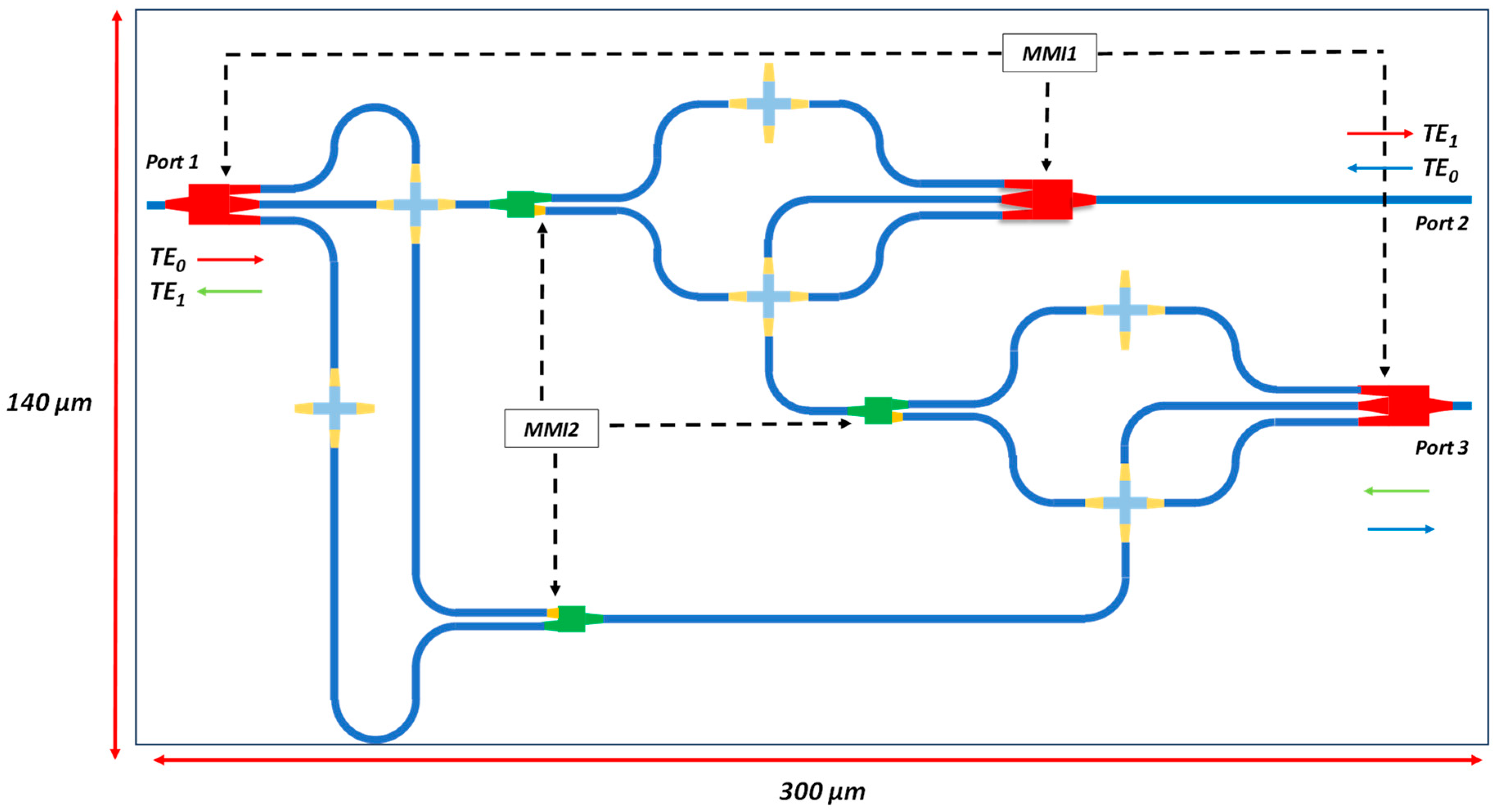
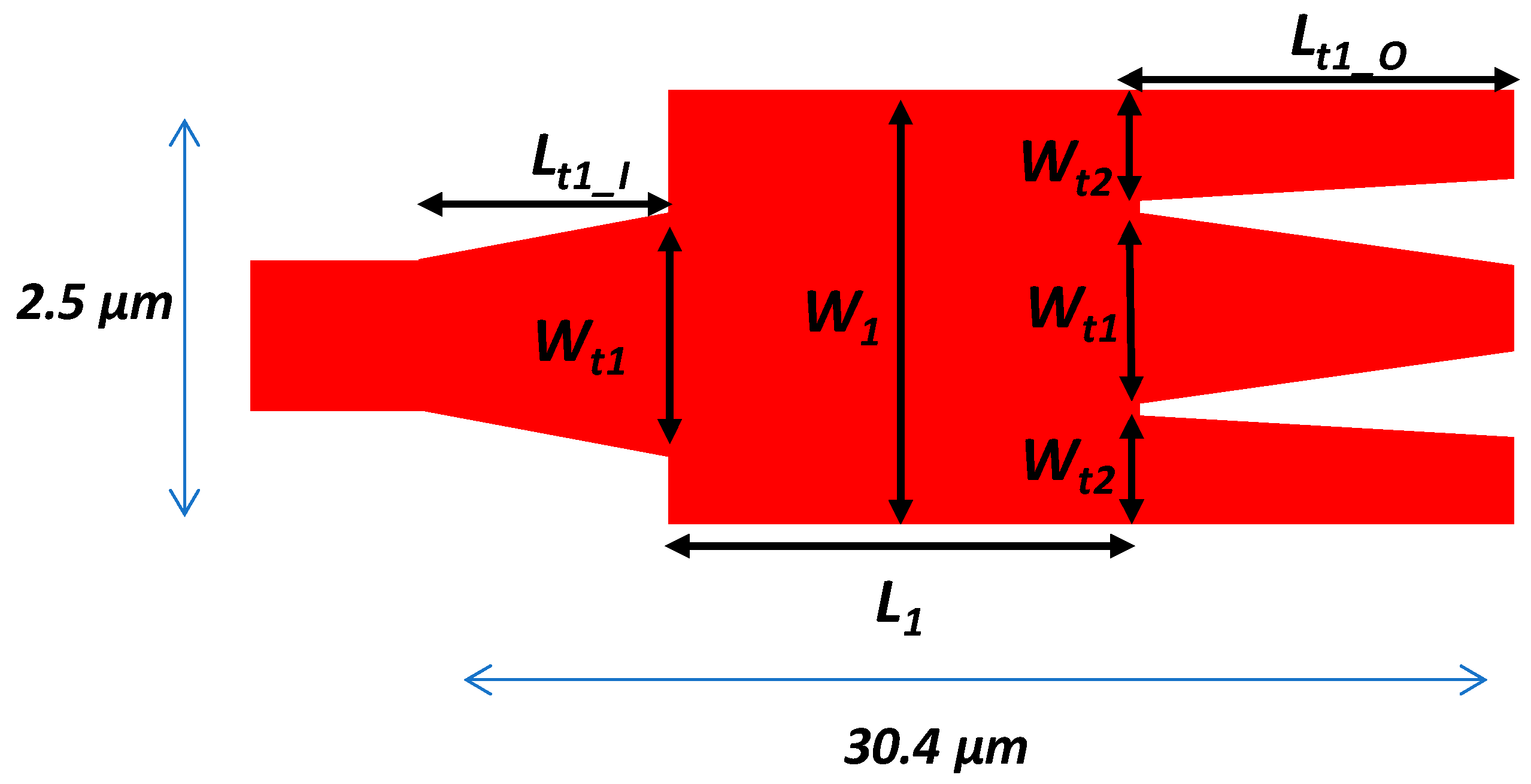
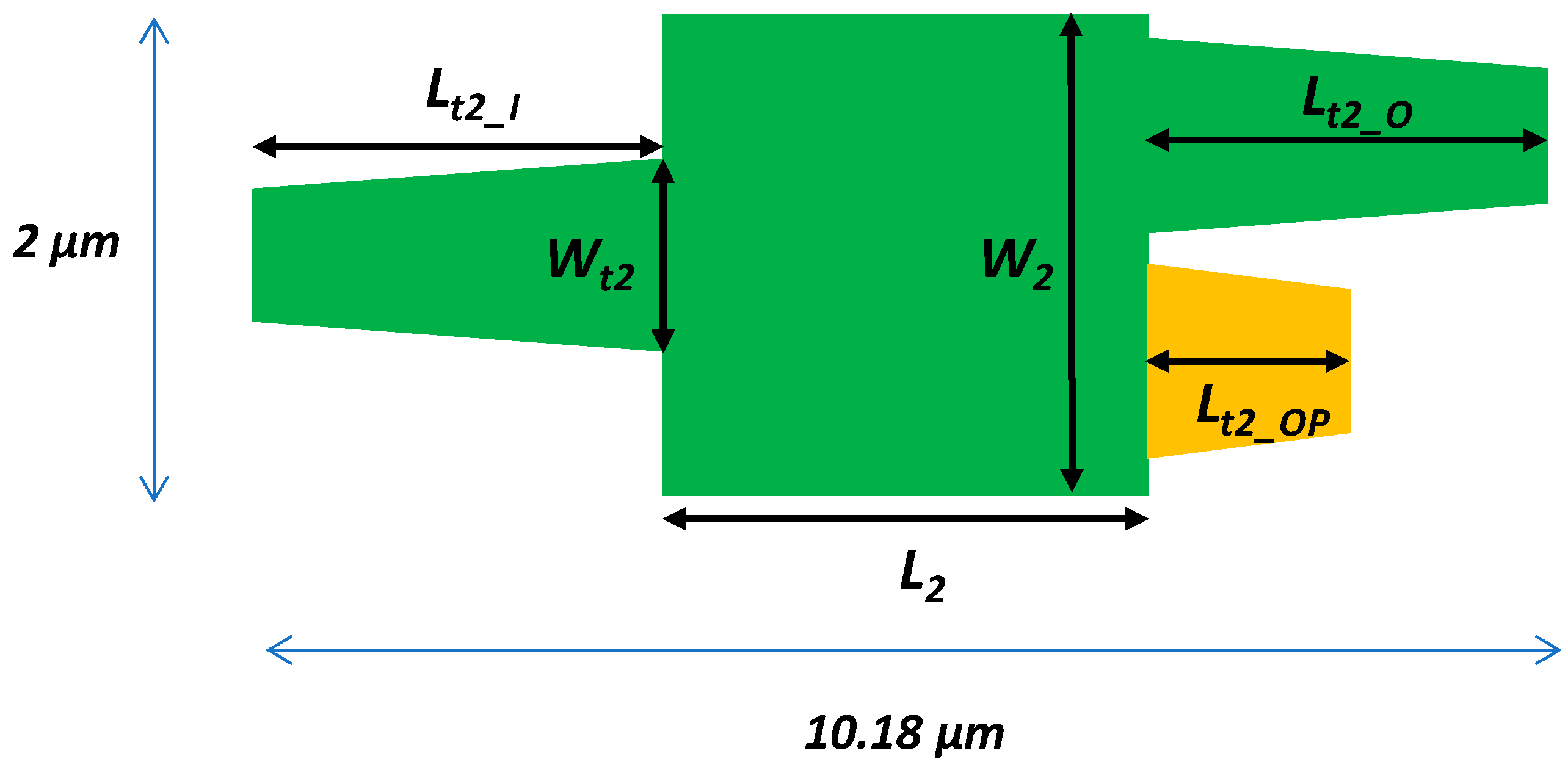
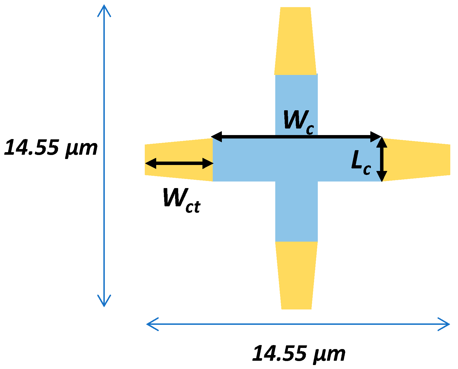
2. Proposed Optical Circulating Network Architecture

The schematic diagram of the proposed SiPh-based optical circulating network is shown in Figure 1. This network employs 1 × 3 MMI1 (in red) at different input/output ports. In addition, it employs 1 × 2 MMI2 (in green) and waveguide crossings (in yellow and light blue). The design of the device is based on an SOI platform with a 2 μm BOX, and the silicon component thickness is 220 nm. This is compatible with most silicon photonics fabrication foundries. The overall dimensions of the component are 140 μm × 300 μm, as shown in Figure 1. In this study, we evaluate the performance of the optical circulating network via an Ansys® Lumerical® Finite-Difference Time-Domain (FDTD) simulation.
As shown in Figure 1, the optical circulating direction is from Port 1 to Port 2 (red arrows); from Port 2 to Port 3 (blue arrows); and from Port 3 to Port 1 (green arrows). The operation principle of the proposed device is detailed as follows. First of all, the optical signal input at Port 1 of the device will be launched into MMI1. By designing the proper parameters of the MMI1, no mode conversion occurs when the transverse electric zero mode (TE0) propagates through the first MMI1 from left to right. Then, the optical signal will be launched into MMI2 via a waveguide crossing. MMI2 will equally power divide the signal into two output ports. The use of different taper lengths at MMI2 is to provide different phase shifts for the two output TE0 signals. The two TE0 signals, propagating in the upper and lower arms, will then be combined in the second MMI1, which is positioned at a 180° rotation with respect to the first MMI1. The two TE0 signals will mode combine to be a TE1 signal and then output at Port 2 of the device. Hence, signal transmission and mode conversion from Port 1 to Port 2 is achieved. When the TE0 optical signal is input at Port 2 of the device, similarly, it will be launched into MMI1, and no mode conversion occurs. Then, the optical signal will be launched into MMI2 via a waveguide crossing. This MMI2 will also equally power divide the signal into two output ports. The two TE0 signals, propagating in the upper and lower arms, will be combined in the third MMI1 at Port 3, which has the same orientation as the second MMI1. Hence, the signal launched at Port 2 will transmit to Port 3 and will be blocked at Port 1, achieving optical circulation.
Figure 2 illustrates the design of the 1 × 3 MMI1. The optical power division and mode combination capabilities can be achieved using self-imaging inside the multi-mode interference region [32,33]. Inside the MMI, the field at position z along the propagation direction can be represented in Equation (1),
ψ x , z = υ C υ φ υ x   e i β υ Z = υ C υ φ υ x   exp [ i υ ( υ + 2 ) π 3 L π Z ]   e i β 0 Z
where L π = π β 0 β 1 is the beat length between the zero and first-order modes, and β is the propagation constant of that mode. C υ is the excitation coefficient, and φ υ x is the normalized mode profile. We can observe that when the inputted electric field enters the TE0 mode at x = 0, it will reappear symmetrically at Z = 3 L π 4 . Similarly, when TE1 light is inputted at x = 0, it will generate an antisymmetric image at Z = 3 L π 4 . On both sides of the waveguides, it will split into two TE0 modes with a phase difference of π. The design parameters of MMI1 after optimization by the simulation are W1 = 2.5 μm, L1 = 10.4 μm, Wt1 = 1.2 μm, Lt1-I = 8 μm, and Lt1-O = 12 μm. In MMI1, the width of the taper is Wt1 = 1.2 μm, which is about half of the width of the MMI, W1 = 2.5 μm. The width of the interconnected waveguides after the taper is 0.4 μm.
After the TE0 mode passes through the first MMI1, in order to successfully enter the second MMI1 for mode combination, it is necessary to power divide the TE0 mode at the top and bottom ports. Here, we utilize a 1 × 2 MMI for beam splitting. Figure 3 illustrates the design parameters of 1 × 2 MMI2, where W2 = 2 μm, L2 = 3.18 μm, Wt2 = 0.6 μm, Lt2-I = 3 μm, Lt2-O = 4 μm, and Lt2-OP = 1.2 μm. In addition, in order to achieve the required phase difference for the mode combination in the second MMI1, different taper lengths are used at the output as a phase shifter to generate a phase difference of π.
In the proposed optical circulating network, the bent waveguide sections are configured with a bend radius of 10 µm. In addition, after passing through MMI2, in order to maintain the same optical paths in the upper and lower arms, a dummy waveguide crossing is employed in the upper arm. In the crossing section, the design is based on the principle of multimode interference [34], with the design parameters shown in Figure 4, where Wc = 8.55 µm, Wt = 1.8 µm, and Wct = 3 µm.

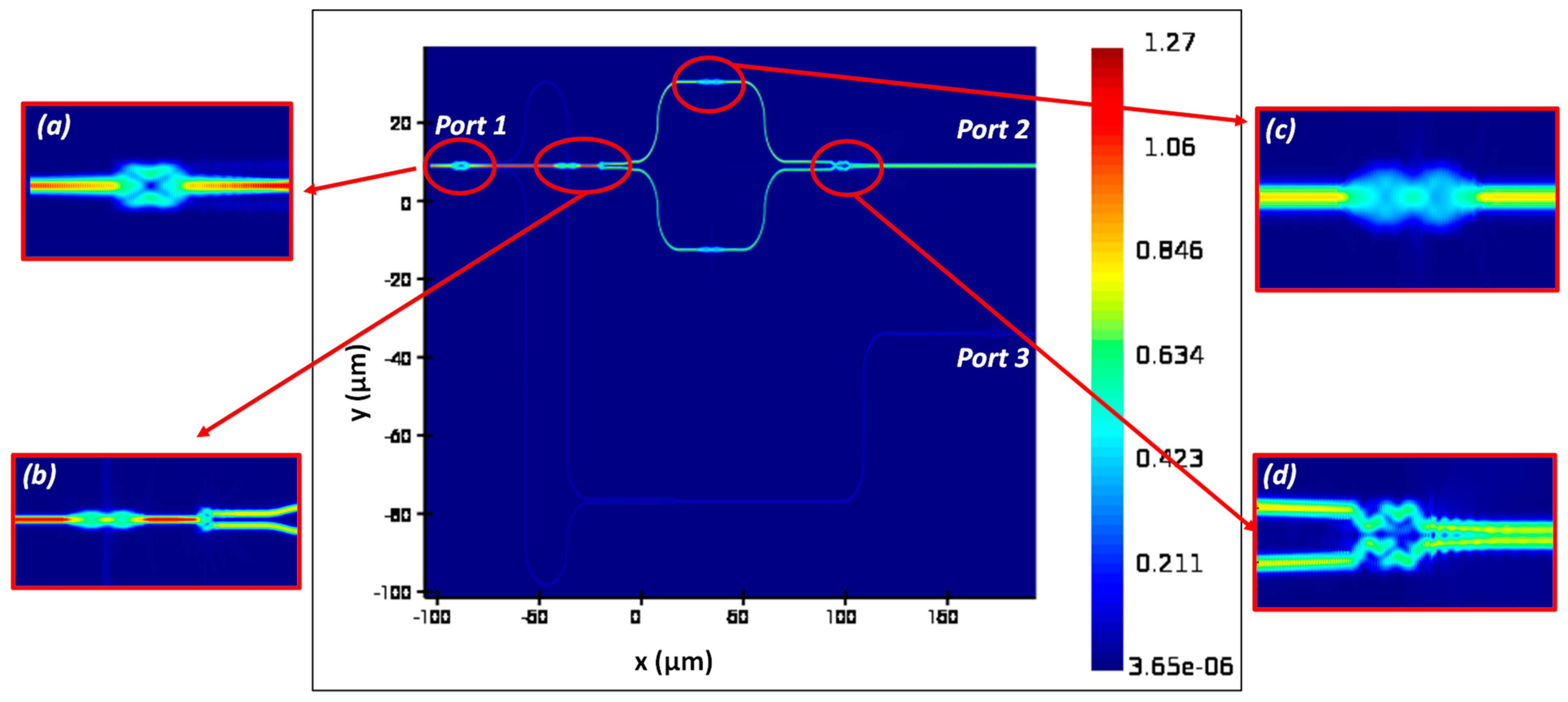
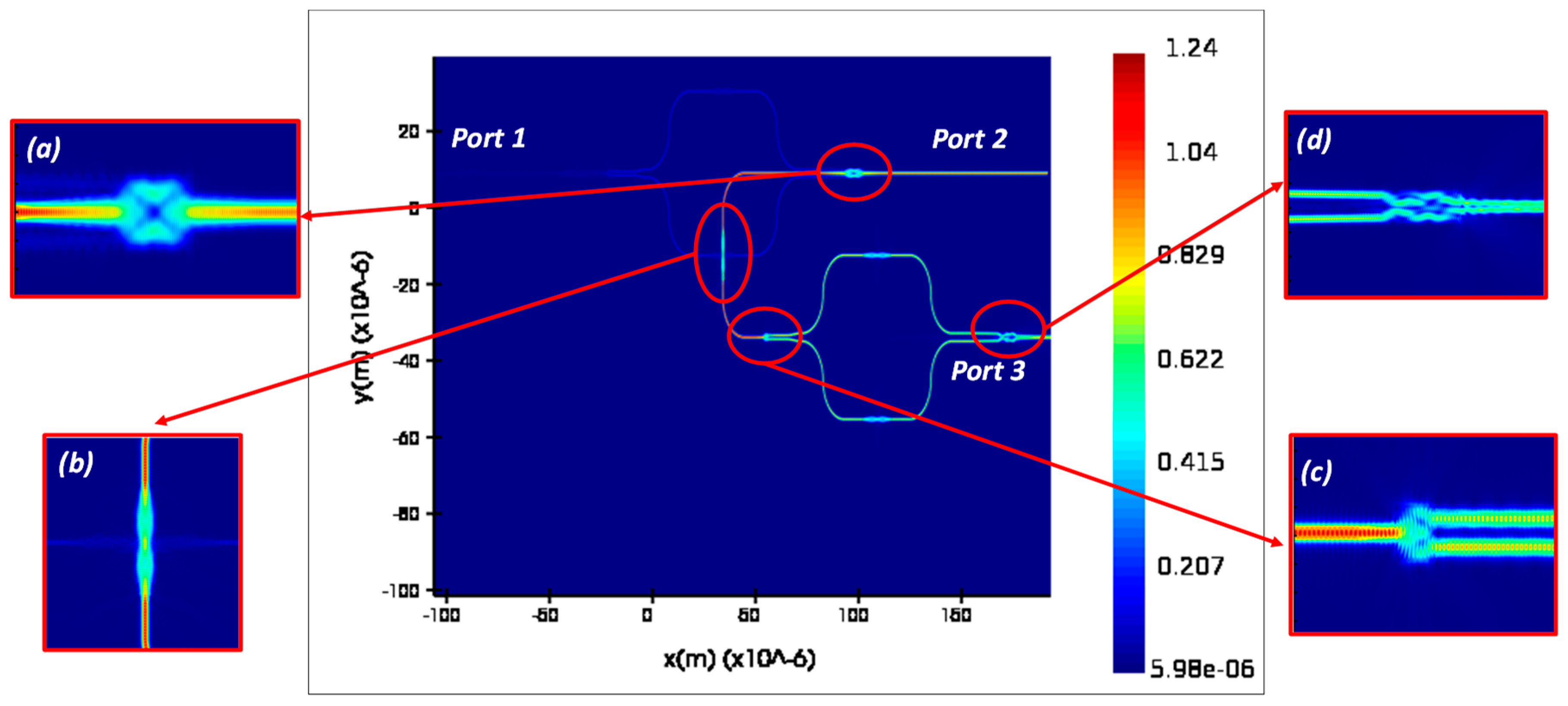
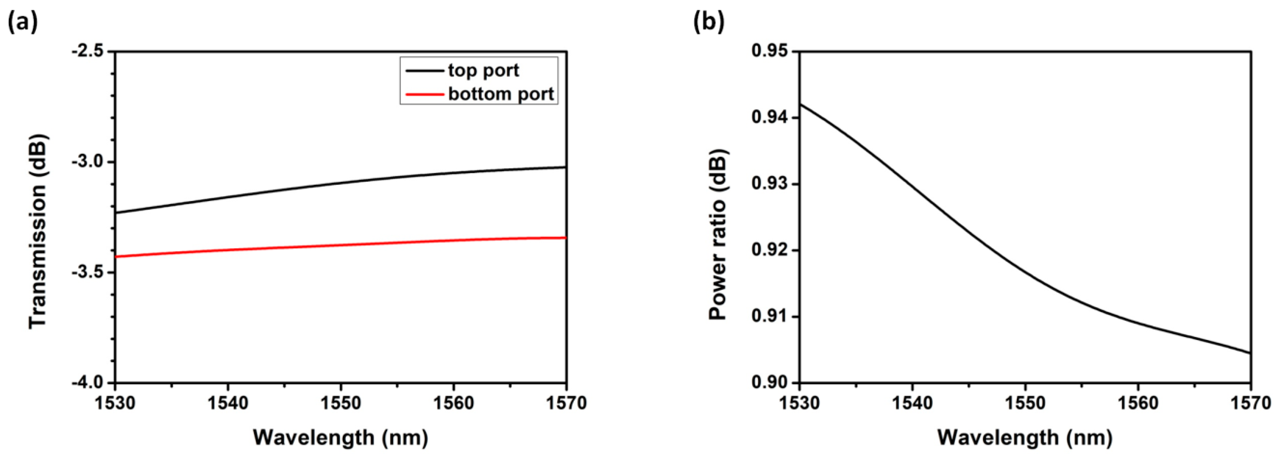
3. Demonstration, Results, and Discussion

Figure 5 illustrates the FDTD simulation results of the entire optical circulating network when an optical signal is launched from Port 1 and output at Port 2. In this work, the simulations are performed in 3D FDTD using the commercially available simulation software Lumerical®. Figure 5 and Figure 6 present the electric field (E-field) propagations obtained via simulation. The simulation is carried out in a 3D model using the effective refractive index of the materials for the simulation. The simulations in Figure 5 and Figure 6 are performed by launching the Lumerical® built-in broadband light source at a wavelength range of 1530 to 1570 nm. Insets of Figure 5a–d, respectively, reveal different components inside the optical circulating network, including the first MMI1 that allows the TE0 mode optical signal to pass through, the MMI2 for power division, the waveguide crossing, and the second MMI1 for mode combination. Similarly, Figure 6 illustrates the simulated FDTD field pattern when the optical signal is launched from Port 2 and output at Port 3. Figure 6 also illustrates a negligible optical signal at Port 1. As discussed above, the optical circulating direction is from Port 1 to Port 2; Port 2 to Port 3; and Port 3 to Port 1. Figure 5 and Figure 6 illustrate the optical circulation from Port 1 to Port 2 and Port 2 to Port 3, respectively. Without loss of generality, the proposed network also supports optical circulation from Port 3 to Port 1, achieving similar results as illustrated in Figure 6.
Next, we analyze each component separately. Figure 7a shows the transmission spectrum of the “straight pass” 1 × 3 MMI1 without any mode conversion, when the optical signal is launched at the single input port and measured at the middle output port, at TE0 mode in the C-band wavelength (1530–1570 nm). A very good transmission can be observed in the whole C-band wavelength, with the highest transmission loss being 0.25 dB. In addition, Figure 7a shows the transmission spectrum when the same design of MMI1 is used for TE1 mode generation. Good transmission can also be observed in the whole C-band wavelength, with the highest transmission loss being ~0.4 dB. Figure 7b shows the crosstalk of MMI1 measured at the top and bottom output ports. Both the top (in black) and bottom (in green) curves overlap, illustrating the symmetric performances of the two output ports. In addition, a high isolation of ~20 dB can be observed at the middle output port with respect to both the top and bottom ports in the 40 nm wavelength range, illustrating low crosstalk. The proposed optical circulating network is designed to reduce the footprint of the entire structure; hence, we optimize the device in the C-band wavelength window. Therefore, while the results obtained via simulation may not show the best transmission performance at the particular wavelength of 1550 nm, the parameters obtained within the C-band wavelength range should be considered the optimal results.
We will now study the fabrication error tolerance of the MMI. As illustrated in Figure 2, the width W1 of the rectangular region in MMI1 varies with different additional widths of ΔW, and the widths of the tapers are adjusted accordingly. Figure 8a shows the fabrication tolerance of the “straight pass” 1 × 3 MMI1 without any mode conversion (TE0 to TE0) when the optical signal is launched at the single input port and measured at the middle output port. We can observe that the transmission variation is within 0.8 dB when the fabrication error is ±0.1 μm. Figure 8b shows the fabrication tolerance of the 1 × 3 MMI1 when it is used for TE1 mode generation (TE0 to TE1) when 2 TE0 optical signals are launched at the top and bottom ports on the right-hand side of Figure 2 and measured at the single output port on the left-hand side of Figure 2. We can observe that the transmissions vary significantly. At a 1550 nm wavelength, the transmission variation is 3 dB when the fabrication error is ±0.1 μm.
In SOI platforms, there are two common choices for patterning the silicon: electron-beam lithography (EBL) [35] and deep-ultraviolet (DUV) lithography [36]. EBL is implemented by writing the design directly onto the resist via an electron beam. This can provide high-precision and high-accuracy (i.e., sub-10 nm [35]) patterning. However, EBL is not suitable for the high-volume manufacturing of devices due to low processing speeds and high cost. In contrast, DUV lithography performs patterning using masks, which expose the resist via exposures. Hence, DUV lithography demonstrates high speed and low cost for mass production. However, DUV lithography has a relatively large minimum feature size and fabrication error. In [36], the minimum feature of an SOI device using DUV lithography is ~100 nm. Therefore, in Figure 8a,b, we outline the fabrication errors from ±50 nm to ±100 nm.
Figure 9a shows the transmission spectrum of MMI2. As discussed in Figure 3 above, a phase shift must be implemented at the output ports of MMI2 in order to have successful mode combination in the second MMI1. This phase shift is accomplished using different taper lengths. As the bottom output port has a much shorter taper length, there is an additional power loss of approximately 0.2–0.3 dB at the bottom output port, as shown in Figure 9a. An intrinsic 3 dB loss is also observed at each output port due to optical power division. The output power contrast ratio (i.e., the ratio of power output from the two paths of the 1 × 2 MMI after passing through the phase shifter) between the two ports is approximately 1:0.92 at a wavelength of 1550 nm, as shown in Figure 9b. In addition, successful optimization has been achieved in the waveguide crossing, and the output port loss is <0.14 dB in the C-band window, as shown in Figure 10a. Figure 10b shows the power leakage measured at the top and bottom ports of the waveguide crossing when the TE0 mode input is launched at the left/right port. Low transmission of <−39 dB can be observed at both the top and bottom ports of the waveguide crossing in the 40 nm wavelength range, illustrating negligible optical signal leakage.
Finally, we evaluate the entire proposed optical circulating network. Figure 11a shows the transmission spectra of the proposed optical circulating network when the optical signal is launched at Port 1 and measured at Port 2, or when the optical signal is launched at Port 2 and measured at Port 3. We can observe that the transmission losses at each output port remain at around 1 to 2 dB within the C-band wavelength range. In addition, we also evaluate optical isolation. Figure 11b shows the optical isolation of the proposed optical circulating network when the optical signal is launched at Port 1 and measured at Port 3, or when the optical signal is launched at Port 2 and measured at Port 2. Very good isolation of >35 dB can be observed in both cases. Figure 11a shows the transmission spectra of the entire optical circulating network from Port 1 to Port 2, and from Port 2 to Port 3, while Figure 11b shows the corresponding reflection spectra of the entire optical circulating network. Some ripples can be observed in both spectra. This is because the proposed optical circulating network is designed to reduce the footprint of the entire structure while satisfying the constraints of the component manufacturing process specifications, as well as achieving acceptable transmission/isolation performances. Hence, sharp bends are unavoidable at several locations in the device, and these bends produce ripples. The ripples in the transmission and reflection spectra could be reduced by lengthening the entire device so that sharp bends can be avoided.
The primary function of the device is to perform optical circulation. The optical circulating direction is from Port 1 to Port 2, or from Port 2 to Port 3. The 1 × 3 MMI1 alone can also be utilized as the MDM multiplexer/de-multiplexer. For the multiplexing operation, by launching TE0 at the middle port at right-hand side of Figure 2, it will “straight pass” to the output port on the left-hand side of Figure 2. Then, 2 TE0 optical signals are launched at the top and bottom ports on the right-hand side of Figure 2, and a TE1 signal is produced at the left-hand side of Figure 2. As a result, MDM multiplexing of TE0 and TE1 can be achieved. Similarly, for the de-multiplexing operation, both TE0 and TE1 optical signals are launched from the left-hand side of Figure 2, and TE0 will be obtained in the middle output port, while the TE1 down-converted TE0 signal will be observed at both the top and bottom output ports on the right-hand side of Figure 2. The proposed optical circulating network has potential to be used in optical fiber networks to separate the upstream and downstream signal transmissions. In addition, it has potential to be used in an optical add-drop multiplexer (OADM) for signal add/drop.

4. Conclusions

Increasing transmission capacity and improving spectral efficiency are important research directions in interconnection networks and system-on-chip networks. However, as the complexity of integrated photonic chip designs continues to increase, the crosstalk among different optical components becomes severe. In order to increase capacity while simultaneously reducing the functional disruption caused by crosstalk and interference, optical circulating components with the ability to control specific optical transmission directions are required. Currently available optical circulators are made up of bulk optics, including Faraday rotators, wave plates, polarization beam splitters, etc. However, achieving passive, all-silicon optical circulators on an SOI platform still presents many challenges. Through simulation, we proposed and demonstrated a passive SiPh-based optical circulating network on an SOI platform. The proposed device is made up of two MMI structures and waveguide crossings. The “straight pass” operation of 1 × 3 MMI1 has a low transmission loss of <0.25 dB and a high isolation of 20 dB at both the top and bottom ports in the 40 nm wavelength range. When the MMI1 is in mode combination operation, a transmission loss of <0.4 dB is observed. The 1 × 2 MMI2 has an intrinsic 3 dB loss at each output port due to optical power division. As the bottom output port of MMI2 has a much shorter taper length for the realization of phase shift, there is an additional power loss of approximately 0.2–0.3 dB at the bottom output port. The waveguide crossing has a loss of <0.14 dB in the C-band window, and a low transmission of <−39 dB at both the top and bottom ports. Finally, the entire optical circulating network has a loss of 1.5 dB at each output port, while demonstrating a high isolation of 35 dB in the C-band transmission window from 1530 nm to 1570 nm. Moreover, the proposed on-chip optical circulating network has several advantages. It is fully passive, and no active control is needed. It is compact, with dimensions of 140 μm × 300 μm. The proposed device also complies with the design rules of most silicon photonics fabrication foundries. In order to achieve broader operating bandwidths, the effective refractive index of the device could be modified. This can be achieved by increasing the waveguide height [37] or employing sub-wavelength waveguide structures [38].

Author Contributions

All authors contributed to the study conception and design. Material preparation, data collection, and analysis were performed by Y.-Z.L., J.-W.C., C.-H.Y. and C.-W.C. The first draft of the manuscript was written by Y.-Z.L., and all authors commented on previous versions of the manuscript. All authors have read and agreed to the published version of the manuscript.

Funding

This work was supported by National Science and Technology Council, Taiwan, under Grant NSTC-112-2221-E-A49-102-MY3, NSTC-110-2221-E-A49-057-MY3.

Institutional Review Board Statement

Not applicable.

Informed Consent Statement

Not applicable.

Data Availability Statement

The data presented in this study are available from the first author upon request.

Conflicts of Interest

The authors declare no conflict of interest.

References

  1. Soref, R. The Past, Present, and Future of Silicon Photonics. IEEE J. Sel. Top. Quantum Electron. 2006, 12, 1678–1687. [Google Scholar] [CrossRef]
  2. Jalali, B.; Fathpour, S. Silicon Photonics. J. Lightw. Technol. 2006, 24, 4600–4615. [Google Scholar] [CrossRef]
  3. Dai, D.; Liang, D.; Cheben, P. Next-generation silicon photonics: Introduction. Photon Res. 2022, 10, NGSP1–NGSP3. [Google Scholar] [CrossRef]
  4. Tsang, H.K.; Liu, Y. Nonlinear optical properties of silicon waveguides. Semicond. Sci. Technol. 2008, 23, 064007. [Google Scholar] [CrossRef]
  5. Tsang, H.K.; Chen, X.; Cheng, Z.; Zhou, W.; Tong, Y. Subwavelength Silicon Photonics. In Silicon Photonics IV: Innovative Frontiers; Topics in Applied Physics; Springer: Cham, Switzerland, 2021; Volume 139, pp. 565–572. [Google Scholar]
  6. Shahbaz, M.; Butt, M.A.; Piramidowicz, R. Breakthrough in Silicon Photonics Technology in Telecommunications. Bio-sensing, and Gas Sensing. Micromachines 2023, 14, 1637. [Google Scholar] [CrossRef]
  7. Hashemi, H. A Review of Silicon Photonics LiDAR. In Proceedings of the 2022 IEEE Custom Integrated Circuits Conference (CICC), Newport Beach, CA, USA, 21–24 April 2024; pp. 1–8. [Google Scholar]
  8. de Lima, T.F.; Shastri, B.J.; Tait, A.N.; Nahmias, M.A.; Prucnal, P.R. Progress in neuromorphic photonics. Nanophotonics 2017, 6, 577–599. [Google Scholar] [CrossRef]
  9. Sajan, S.C.; Singh, A.; Sharma, P.K.; Kumar, S. Silicon Photonics Biosensors for Cancer Cells Detection—A Review. IEEE Sensors J. 2023, 23, 3366–3377. [Google Scholar] [CrossRef]
  10. Siew, S.Y.; Li, B.; Gao, F.; Zheng, H.Y.; Zhang, W.; Guo, P.; Xie, S.W.; Song, A.; Dong, B.; Luo, L.W.; et al. Review of Silicon Photonics Technology and Platform Development. J. Light. Technol. 2021, 39, 4374–4389. [Google Scholar] [CrossRef]
  11. Li, C.; Dai, D. Compact polarization beam splitter for silicon photonic integrated circuits with a 340-nm-thick silicon core layer. Opt. Lett. 2017, 42, 4243–4246. [Google Scholar] [CrossRef]
  12. Dai, D.; Wang, J.; Shi, Y. Silicon mode (de)multiplexer enabling high capacity photonic networks-on-chip with a sin-gle-wavelength-carrier light. Opt. Lett. 2013, 38, 1422–1424. [Google Scholar] [CrossRef]
  13. Li, C.-L.; Jiang, X.-H.; Hsu, Y.; Chen, G.-H.; Chow, C.-W.; Dai, D.-X. Ten-channel mode-division-multiplexed silicon photonic integrated circuit with sharp bends. Front. Inf. Technol. Electron. Eng. 2019, 20, 498–506. [Google Scholar] [CrossRef]
  14. Stern, B.; Zhu, X.; Chen, C.P.; Tzuang, L.D.; Cardenas, J.; Bergman, K.; Lipson, M. On-chip mode-division multiplexing switch. Optica 2015, 2, 530–535. [Google Scholar] [CrossRef]
  15. Hsu, Y.; Chuang, C.-Y.; Wu, X.; Chen, G.-H.; Hsu, C.-W.; Chang, Y.-C.; Chow, C.-W.; Chenb, J.; Lai, Y.-C.; Yeh, C.-H.; et al. 2.6 Tbit/s On-Chip Optical Interconnect Supporting Mode-Division-Multiplexing and PAM-4 Signal. IEEE Photon-Technol. Lett. 2018, 30, 1052–1055. [Google Scholar] [CrossRef]
  16. Chen, G.-H.; Tsai, J.-F.; Peng, C.-W.; Kuo, P.-C.; Chen, C.-J.; Chow, C.-W.; Yeh, C.-H.; Lai, Y.; Liu, Y. Compact Mode Division MUX/DEMUX Using Enhanced Evanescent-Wave Coupling on Silicon-on-Insulator (SOI) Platform for 11-Tbit/s Broadband Transmission. IEEE Access 2020, 8, 219881–219890. [Google Scholar] [CrossRef]
  17. Liu, Y.; Wang, X.; Yao, Y.; Du, J.; Song, Q.; Xu, K. Silicon photonic arrayed waveguide grating with 64 channels for the 2 µm spectral range. Opt. Lett. 2022, 47, 1186–1189. [Google Scholar] [CrossRef]
  18. Liu, S.; Hu, H.; Ma, X.; Dong, R.; Fang, Q.; Chen, H. Low-crosstalk silicon-photonics arrayed waveguide gratings integrated with micro-ring filter. Front. Phys. 2022, 10, 1018589. [Google Scholar] [CrossRef]
  19. Liu, J.; Li, S.; Ding, Y.; Chen, S.; Du, C.; Mo, Q.; Morioka, T.; Yvind, K.; Oxenløwe, L.K.; Yu, S.; et al. Orbital angular momentum modes emission from a silicon photonic integrated device for km-scale data-carrying fiber transmission. Opt. Express 2018, 26, 15471–15479. [Google Scholar] [CrossRef]
  20. Jian, Y.H.; Chow, C.W. Design and analysis of a compact micro-ring resonator signal emitter to reduce the uniformi-ty-induced phase distortion and crosstalk in orbital angular momentum (OAM) division multiplexing. Opt. Exp. 2023, 31, 810–825. [Google Scholar] [CrossRef]
  21. Stepanov, I.V.; Fatkhiev, D.M.; Lyubopytov, V.S.; Kutluyarov, R.V.; Grakhova, E.P.; Neumann, N.; Khonina, S.N.; Sultanov, A.K. Wavelength-Tunable Vortex Beam Emitter Based on Silicon Micro-Ring with PN Depletion Diode. Sensors 2022, 22, 929. [Google Scholar] [CrossRef]
  22. Lin, Y.-Z.; Chow, C.-W.; Yu, T.-W.; Jian, Y.-H.; Hung, T.-Y.; Chen, J.-W.; Yeh, C.-H. Flexible Data Rate Allocation Using Non-Orthogonal Multiple Access (NOMA) in a Mode Division Multiplexing (MDM) Optical Power Splitter for System-on-Chip Networks. Sensors 2023, 23, 7259. [Google Scholar] [CrossRef]
  23. Fujii, Y. High-isolation polarization-independent optical circulator. J. Light. Technol. 1991, 9, 1238–1243. [Google Scholar] [CrossRef]
  24. Mitsuya, K.; Shoji, Y.; Mizumoto, T. Demonstration of a Silicon Waveguide Optical Circulator. IEEE Photon-Technol. Lett. 2013, 25, 721–723. [Google Scholar] [CrossRef]
  25. Jalas, D.; Petrov, A.Y.; Eich, M. Optical three-port circulators made with ring resonators. Opt. Lett. 2014, 39, 1425–1428. [Google Scholar] [CrossRef]
  26. Liu, L.; Dong, J.; Gao, D.; Zheng, A.; Zhang, X. On-chip passive three-port circuit of all-optical ordered-route transmission. Sci. Rep. 2015, 5, 10190. [Google Scholar] [CrossRef]
  27. Wang, Q.; Ouyang, Z.; Tao, K.; Lin, M.; Ruan, S. T-shaped optical circulator based on coupled magneto-optical rods and a side-coupled cavity in a square-lattice photonic crystal. Phys. Lett. A 2012, 376, 646–649. [Google Scholar] [CrossRef]
  28. Śmigaj, W.; Romero-Vivas, J.; Gralak, B.; Magdenko, L.; Dagens, B.; Vanwolleghem, M. Magneto-optical circulator designed for operation in a uniform external magnetic field. Opt. Lett. 2010, 35, 568–570. [Google Scholar] [CrossRef]
  29. Richardson, D.J.; Fini, J.M.; Nelson, L.E. Space-division multiplexing in optical fibres. Nat. Photonics 2013, 7, 354–362. [Google Scholar] [CrossRef]
  30. Kuo, P.-C.; Tong, Y.; Chow, C.-W.; Tsai, J.-F.; Liu, Y.; Chang, Y.-C.; Yeh, C.H.; Tsang, H.K. 4.36 Tbit/s Silicon Chip-to-Chip Transmission via Few-Mode Fiber (FMF) using 2D Sub-wavelength Grating Couplers. In Proceedings of the Optical Fiber Communications Conference and Exhibition, OFC 2021, San Francisco, CA, USA, 6–10 June 2021; p. M3D.6. [Google Scholar]
  31. Weng, Y.; Ip, E.; Pan, Z.; Wang, T. Advanced spatial-division multiplexed measurement systems propositions—From telecommunication to sensing applications: A review. Sensors 2016, 16, 1387. [Google Scholar] [CrossRef]
  32. Kawaguchi, Y.; Tsutsumi, K. Mode multiplexing and demultiplexing devices using multimode Interference couplers. Electron. Lett. 2002, 38, 1701–1702. [Google Scholar] [CrossRef]
  33. Soldano, L.B.; Pennings, E.C.M. Optical multi-mode interference devices based on self-imaging: Principles and applica-tions. J. Lightw. Technol. 1995, 13, 615–627. [Google Scholar] [CrossRef]
  34. Johnson, M.; Thompson, M.G.; Sahin, D. Low-loss, low-crosstalk waveguide crossing for scalable integrated silicon pho-tonics applications. Opt. Exp. 2020, 28, 12498–12507. [Google Scholar] [CrossRef]
  35. Hu, W.; Sarveswaran, K.; Lieberman, M.; Bernstein, G.H. Sub-10 nm electron beam lithography using cold development of poly(methylmethacrylate). J. Vac. Sci. Technol. B Microelectron. Nanometer Struct. 2004, 22, 1711–1716. [Google Scholar] [CrossRef]
  36. Lin, S.; Hammood, M.; Yun, H.; Luan, E.; Jaeger, N.; Chrostowski, L. Computational lithography for silicon photonics de-sign. IEEE J. Sel. Top. Quantum Electron. 2020, 26, 8201408. [Google Scholar] [CrossRef]
  37. Lv, D.; Wu, L.; Liu, C.; Li, A.; Wang, R.; Wu, A. Broadband and Low-Loss Silicon Photonic Directional Coupler for Signal Power Tapping on the 3 μm SOI Waveguide Platform. Photonics 2023, 10, 776. [Google Scholar] [CrossRef]
  38. Li, C.; Zhang, M.; Xu, H.; Tan, Y.; Shi, Y.; Dai, D. Subwavelength silicon photonics for on-chip mode-manipulation. PhotoniX 2021, 2, 11. [Google Scholar] [CrossRef]
Figure 1. Schematic diagram of the proposed optical circulating network and mode converter architecture: MMI: multi-mode interferometer. The optical circulating direction is from Port 1 to Port 2 (red arrows); Port 2 to Port 3 (blue arrows); and Port 3 to Port 1 (green arrows).
Photonics 10 01278 g001
Figure 2. Schematic diagram of the MMI1 design.
Photonics 10 01278 g002
Figure 3. Schematic diagram of the MMI2 design.
Photonics 10 01278 g003
Figure 4. Schematic diagram of the waveguide crossing design.
Photonics 10 01278 g004
Figure 5. FDTD simulation results for the proposed optical circulating network from Port 1 to Port 2. Insets: (a) the first MMI1 input, (b) the MMI2 and phase shifter, (c) waveguide crossing, (d) the second MMI1.
Photonics 10 01278 g005
Figure 6. FDTD simulation results for the proposed optical circulating network from Port 2 to Port 3. Insets: (a) the MMI1, (b) waveguide crossing, (c) the MMI2, (d) the second MMI1.
Photonics 10 01278 g006
Figure 7. (a) Transmission spectrum of the “straight pass” 1 × 3 MMI1 without any mode conversion (TE0 to TE0) when optical signal is launched at the single input port and measured at the middle output port. Transmission spectrum MMI1 is used for TE1 mode generation (TE0 to TE1). (b) Crosstalk of MMI1 is measured at the top, middle, and bottom output ports.
Photonics 10 01278 g007
Figure 8. Fabrication tolerance of the (a) “straight pass” MMI1 without any mode conversion (TE0 to TE0) when optical signal is launched at the single input port and measured at the middle output port; (b) MMI1 is used for TE1 mode generation (TE0 to TE1) when 2 TE0 optical signals are launched at the top and bottom ports and measured at the single output port on the other side.
Photonics 10 01278 g008
Figure 9. Performance of the 1 × 2 MMI2 for mode combination. (a) Transmission spectrum when optical signal is launched at a single input port and measured at both output ports. (b) Output power contrast ratio between the two ports.
Photonics 10 01278 g009
Figure 10. Performance of the waveguide crossing. (a) Transmission spectrum when optical signal is launched at the input port and measured at both output ports. (b) Power leakage measured at the top and bottom ports of the waveguide crossing.
Photonics 10 01278 g010
Figure 11. Performance of the entire proposed optical circulating network. (a) Transmission spectrum of the proposed optical circulating network when optical signal is launched at Port 1 and measured at Port 2; or when optical signal is launched at Port 2 and measured at Port 3. (b) The corresponding isolation.
Photonics 10 01278 g011
Disclaimer/Publisher’s Note: The statements, opinions and data contained in all publications are solely those of the individual author(s) and contributor(s) and not of MDPI and/or the editor(s). MDPI and/or the editor(s) disclaim responsibility for any injury to people or property resulting from any ideas, methods, instructions or products referred to in the content.

