Abstract
The growth of nanoscale columnar AlxGa1-xN/AlN heterostructures on the surface of silicon substrates using plasma-activated nitrogen molecular-beam epitaxy was investigated in this work. Silicon substrates include atomic-smooth cSi substrate, Si substrate with a transition layer of porous silicon porSi/cSi and a hybrid substrate involving a silicon carbide layer grown with matched substitution of the atoms on the surface of porous silicon SiC/porSi/cSi. A complex analysis performed using a set of structural and spectroscopic techniques demonstrated that the epitaxial growth of the nuclear AlN layer on all types of the substrates in a N-enriched environment resulted in the formation of AlxGa1-xN/AlN heterostructures with a Ga-polar surface, which was realized only on the SiC/porSi/cSi substrate. The layer of AlxGa1-xN on cSi and porSi/cSi substrates was in the state of disordered alloy with an excess of gallium atom content. It was shown that a great difference in the lattice parameters of a substrate–film pair resulted not only in the appearance of a number of various defects but also in a considerable effect on the chemical process of the formation of the alloys, in our case, the AlxGa1-xN alloy. It was shown that nanoscale columns of AlxGa1-xN formed on SiC/porSi/cSi substrate were inclined relative to the c-axis, which was connected with the features of the formation of a SiC layer by the matched substitution of the atoms on the porous Si substrate, resulting in the formation of the inclined (111) SiC facets at the boundary of the (111) Si surface and pores in Si. Optical studies of the grown samples demonstrated that the optical band-to-band transition for the AlxGa1-xN alloy with Eg = 3.99 eVB was observed only for the heterostructure grown on the SiC/porSi/cSi substrate. A qualitative model is proposed to explain the difference in the formation of AlxGa1-xN layers on the substrates of cSi, porSi/cSi and SiC/porSi/cSi. The results obtained in our work demonstrate the availability of using SiC/porSi/cSi substrates for the integration of silicon technology and that used for the synthesis of nanoscale columnar AlxGa1-xN heterostructures using plasma-activated molecular-beam epitaxy with a nitrogen source.
1. Introduction
Active development of the approaches for the epitaxial growth of heterostructures on the basis of semiconductor compounds and nitrides of III-rd elements in the periodic table (AIIIN) has made it possible to design and produce devices with a wide range of applications: ultra-high frequency transistors with a high electron mobility (HEMT), light-emitting diodes (LEDs) operating in UV, visible and IR spectral ranges, detectors for voltage-modulated light sources and so on [1,2,3]. It is supposed that in the future, AIIIBV will be able to replace Si as the material of a channel in a new type of field-effect transistor on the basis of nanowires or even in tunnel field-effect transistors [4,5,6].
Therefore, the integration of AIIIN semiconductor materials with silicon chips intended for signal processing opens a wide field for the appearance of new functional devices [7,8]. In particular, the formation of electromagnetic radiation sources on the basis of nitride compounds formed on silicon substrates would probably enhance the facilities of silicon photonics and start optical data transmission just inside the microelectronic chips [9]. The development of epitaxial technologies for the integration of AIIIN compounds and silicon drastically changes our ideas about photonics in the future [10].
The absence of polarity for Si substrates allows the growth of both Ga- and N-polar structures based on GaN on these structures. Most of the instrument structures are usually known to use 2D Ga-polar heterostructures grown with vapor phase epitaxy from metal–organic substances (VPE-MOS) [11] since they usually show the best morphological and electrophysical characteristics. However, there exists a whole range of applications where N-polar compounds show certain advantages [12,13]. Therefore, this is the reason that recently more and more attention has been drawn to the problems of controlling polarity during the epitaxial synthesis of AIIIN compounds. We have previously shown the possibility of growing GaN layers with Ga- and N-polarity on silicon substrates with molecular-beam epitaxy using plasma-activated nitrogen (MBE-PA). Moreover, a potential possibility has been shown for the separation of the top thick Ga-polar GaN layer grown with chloride–hydride epitaxy from SiC/Si(111) substrate, using an etching intermediate GaN layer from the opposite side with N-polarity, synthesized with the MBE-PA technique.
However, the problems of monolithic integration of photon devices based on nitrides of the third group in the periodic table with silicon substrates are not solved yet. Recently performed investigations demonstrate that some of these fundamental problems can be solved in principle with the use of AIIIN nanoscale structures (nanowhiskers, nanocrystals, nanocolumns) which are epitaxially grown on lattice-mismatched substrates such as silicon and sapphire; they have relatively high crystal quality due to the efficient relaxation of the elastic stresses due to 3D island growth [14].
MBE PA technology is known to provide different stoichiometric growth conditions characterized by the ratio of the flow intensities of third group atoms (FIII) and activated nitrogen (FN), coming in at the growth surface and forming AIIIN layers, with nanocolumnar and smooth morphology without pre-epitaxial masking of the Si(111) substrate. However, it is also known that within the production MBE PA units, the growth of nitride compounds mainly takes place with the use of low streamlets of activated nitrogen, meaning low growth rates of <0.1 μm/h. On the one hand, this means the possibility of a precise control for the thickness of the layers at about 1–2 monolayers when performing MBE PA synthesis of quantum-dimensional heterostructures based on GaN. On the other hand, low growth rates considerably limit the possibility of using thick buffer layers grown on the substrates in order to decrease the defect density in the upper layers of the instrumental epitaxial heterostructures. At the same time, for example, in [13], the availability of the use of island ultra-thin GaN nanostructures grown directly on silicon substrates using MBE PA was demonstrated for creating detectors for UV radiation. In our work, we synthesized island AlxGa1-xN/AlN nanoheterostructures which, unlike more popular nanostructures with a high aspect ratio, such as nanowhiskers, nanocolumns, and so on, are characterized by a low aspect ratio. They were also grown without the use of thick epitaxial buffer layers in order to complete the device production process based on these materials, the first of which being detectors of UV radiation, the most economical and rapid one. Thus, the purpose of this work was to study the possibility of the epitaxial synthesis of ultrathin epitaxial AlxGa1-xN/AlN heterostructures with an acceptable crystal quality on silicon substrates with different modifications of the surface (smooth, porous, with the upper SiC layer) in a single growth process, i.e., in, at most, close-like growth conditions as well as their comprehensive study.
A set of our studies recently performed concerning the growth of nanocolumnar GaN layers synthesized on hybrid SiC/por-Si/c-Si substrates [15] using the MBE PA technique demonstrated the availability of such an approach for the integration of GaN technology with the processes of silicon technology and the requirements of performing further investigations in this direction.
Hence, the aim of our work is to perform a comparative study of nanoscale columnar AlxGa1-xN heterostructures grown using the MBE PA technique on silicon substrates with different surface modifications: a standard surface, atomically smooth cSi with a transition layer of porous silicon porSi/cSi, as well as on the hybrid substrate involving a silicon carbide layer grown on the surface of silicon, namely, SiC/porSi/cSi.
2. Materials and Methods
AlxGa1-xN/AlN heterostructures were grown using molecular-beam epitaxy with a plasma-activated nitrogen source (MBE PA) applying the industrial type unit Veeco Gen 200 in the common epitaxial process. Before the growth of heterostructures, several standard growing experiments were carried out in order to calibrate the basic technological parameters of the industrial unit. To control the stability and calibration of the equivalent pressures for aluminum (FAl) and gallium (FGa) flows, a mobile Bayard–Alpert ionization sensor was used with a measurement range from 10−3 to 10−9 Torr, which was placed in front of the main shutter, in fact, at the point of a substrate arrangement. With the use of an IR pyrometer and W-Re thermocouple, the temperatures of all the substrates used in the experiments were measured (GaN/c-Al2O3, cSi, porSi/cSi, SiC/porSi/cSi). It should be noted that the calibration procedure of the main technological parameters for the MBE PA unit Veeco Gen [16,17] used in the work is regularly performed in order to exclude their uncontrollable changes and provide a stable reproducibility of the obtained results. This was certified in the calibration experiments on the growth of AlN and GaN on the virtual substrates of GaN/c-Al2O3.
Particularly, in the calibration experiments concerning the determination of FAl, FGa and FN in the units of the growth rates of AlN and GaN, virtual GaN/c-Al2O3 substrates were used to minimize crystal lattice parameter mismatching between the AlN and GaN layers with the substrate. To determine the maximum flow of the activated nitrogen, several technological experiments were performed connected with the growth of binary AlN and GaN compounds in the metal-enriched condition (meaning that FIII > FN) under the same temperature of the substrate (T = 660 °C), excluding active desorption of Ga and Al adatoms from the growing surface. In each of the experiments, AlN or GaN was grown at the constant value of high-frequency (HF) power of the plasma source and the same molecular nitrogen gas flow. In the frameworks of the performed experiments, the values of the HF power of the plasma source and gas flow of molecular nitrogen varied. The values of thickness and growth rates of the obtained layers, respectively, were determined using ex situ measurements of scanning electron microscopy. It was found that the maximum value for the flow of activated nitrogen attainable in a certain configuration of the technological unit was FN~0.04–0.05 μm/hour.
A similar approach was used for the determination of FAl and FGa flows in the measurement units of the growth rate of AlN or GaN. In this case, the growth of AlN or GaN layers on the virtual substrates of GaN/c-Al2O3 was completed with the use of nitrogen-enriched conditions (FIII < FN), controlled in situ with the 3D diffraction pattern of the fast-reflected electrons.
In order to grow the studied AlxGa1-xN/AlN heterostructures, Si(111) substrates were used with different modifications of their surface: standard smooth cSi substrates, Si(111) substrates with porous silicon por-cSi formed on their surface as well as SiC/porSi/cSi substrates, where the SiC layer was formed on their surface with the use of consistent substitution of atoms.
Before the MBE PA synthesis of GaN, cSi substrates were prepared according to the Shiraki technique. porSi and SiC/porSi/cSi substrates were degreased. Next, all of the substrates were loaded into one substrate holder of an MBE PA unit and after that, they were annealed in the pre-annealing chamber at 200 °C.
Then the substrates were transported to the main growing chamber of the MBE PA unit, where they first were subjected to pre-epitaxial preparation, involving nitridization of the substrates’ surface in the flow of activated nitrogen. It should be noted that in the described experiments, nitridization of the substrates proceeded at the closed shutter of the nitrogen source; therefore, according to some data from the literature, this can result in the formation of a high-quality SiN layer on the surface of silicon substrates [18]. It should be noted that the substrates involving the SiC layer do not react with nitrogen at this temperature, so they were annealed only for the “purity” of the experiment.
The nitridization process was performed at the temperature of a substrate measured with an IR pyrometer: T~670 °C for 30 min. Parameters of the plasma source (HF power and nitrogen flow) used for nitridization and the following growth of AlxGa1-xN/AlN heterostructures corresponded to the equivalent growth rate of GaN of about FN~0.05 µm/h.
Epitaxial synthesis of heterostructures started from the formation of the nuclear AlN layers on the surface of the substrate at T~800 °C, FAl~0.02 µm/h, grown for 60 min. After that, the temperature of the substrates was lowered to T~700 °C for the growth of the AlxGa1-xN layer for 4 h at the constant values of FAl~0.01 µm/h, FGa~0.4 µm/h and FN~0.04–0.05 µm/h. One should note that in the process of growth, a gradual increase in pyrometer temperature up to T~707 °C was observed. Schematic images of the investigated heterostructures with different kinds of substrates (cSi, porSi/cSi and SiC/porSi/cSi) are presented (see Figure 1).
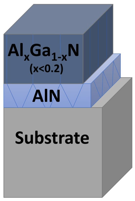
Figure 1.
Schematic image of the studied heterostructures with different types of substrates (cSi, porSi and SiC/porSi/cSi).
Studies of the samples’ structures were performed with the use of high-resolution X-ray diffraction at room temperature. Monochromatic Cu Kα1 radiation (wavelength of 1.54056 Å) and Bruker D8 Discover diffractometer, operating in the parallel beam mode with linear focusing, were utilized in the experiments. The primary beam was subjected to monochromatization with the use of a Ge (220) crystal with double reflection. Pole figures were registered in the precise parallel mode (spot size was 1 mm) with an angular resolution of 1 degree using Ni-filtered CuKα radiation.
Microscopic investigations of heterointerfaces were conducted with an electron microscope, Libra 120 Carl Zeiss (Oberkochen, Germany), while the features of surface morphology were studied with the use of a scanning probe microscope, Femtoscan-001 NT MDT (Bountiful, UT, USA).
The data on the chemical state of surface layers were obtained using X-ray photoelectron spectroscopy (XPS). Spectra were surveyed with the use of an SPECS spectrometer (Berlin, Germany). They were stimulated by Mg Kα-radiation (E = 1253.6 eV). In order to remove possible contaminations of the samples’ surfaces, the latter was irradiated with Ar+ ions with an energy of 4 keV and electron current density of 10 µA/cm2; the rate of layer removal was ~1 nm/min.
The optical properties of the samples were studied within the range of 190–900 nm using ultraviolet (UV) spectroscopy with the use of the unit LAMBDA 650, produced by Perkin Elmer Company (Waltham, MA, USA), provided with the universal URA attachment, allowing us to obtain reflection spectra within the range of the incidence angles from 8 to 80 degrees.
The luminescence spectra of the samples were obtained with the unit Accent RPM Sigma for measuring photoluminescence and optical reflection spectra. The investigations were performed at room temperature under excitation by laser with the wavelength of irradiation equal to 266 nm, W = 5 W/cm2.
3. Results and Discussion
The microstructure as well as the surface morphology of AlxGa1-xN/AlN heterostructures grown on the different types of substrates was studied with the use of scanning electron microscopy (SEM) and atomic force microscopy, respectively.
Figure 2 shows SEM images of the sample chips. From analysis of the images, it follows that all the films are characterized by nanocolumnar morphology. Their thickness is different, and it depends on the type of the substrate used. Moreover, it was found that the thickness of the grown heterostructures was slightly less than expected based on the technological growth conditions. For example, the total thickness of the AlxGa1-xN/AlN heterostructure grown on cSi and porSi/cSi substrates was ~92 and ~94 nm, respectively, while on the SiC/porSi/cSi hybrid substrate, the thickness of the AlxGa1-xN/AlN heterostructure along with the SiC layer was ~140 nm: ~30 nm for the continuous layer of SiC and ~106 nm for the nanocolumnar AlxGa1-xN/AlN heterostructure.
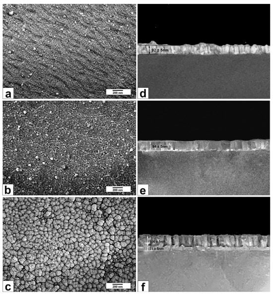
Figure 2.
SEM images of the surface and cross-sections of AlxGa1-xN/AlN heterostructures grown on different substrate surfaces: (a)—cSi; (b)—porSi/cSi and (c)—SiC/porSi/cS with cross-sections for (d)—cSi; (e)—porSi/cSi and (f)—SiC/porSi/cSi.
Note that not only the thickness of the layers but also the morphology of the surface of AlxGa1-xN/AlN heterostructures proved to be dependent on the type of substrate used. Typical images of the surface areas in the films are presented in Figure 3.
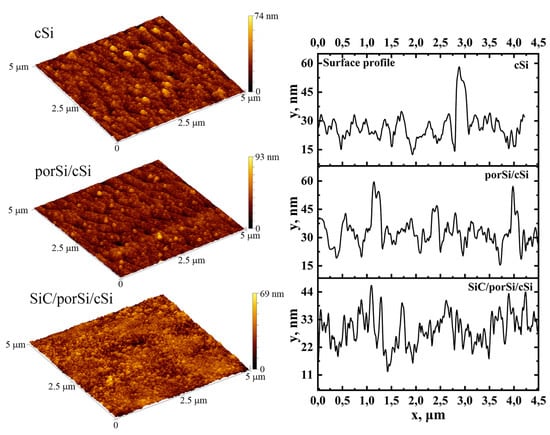
Figure 3.
Typical AFM images of the surface areas, 5 × 5 μm in size (left), and profiles of the surface cross-sections of AlxGa1-xN/AlN heterostructures grown on three types of substrates. Profile of the surface areas of the AlxGa1-xN/AlN heterostructures (right).
Visualization and analysis of the AFM results were performed using a modular program for scanning probe microscopy data—Gwyddion software v2.63. The analysis of AFM images shows that the surface of a sample grown on the cSi substrate is characterized by a comb-like structure. In turn, the ridges of the comb demonstrate a fine-grained structure, where the size of the grains changes within a wide range from several dozen to a hundred nanometers. Clusters with a diameter from 100 to 200 nm are observed at the surface, composed of smaller globules. The height of the globules is 50–60 nm. The surface of the sample porSi/cSi is also characterized by a comb-like structure, where the ridges also have a fine-grained structure just as in the case of the cSi sample. Clusters having a dome-like shape are present with a diameter of 100 to 150 nm, and their mean height is 55–60 nm.
It is noteworthy that nanocolumns of the heterostructure grown on the hybrid SiC/porSi/cSi substrate are arranged most tightly. The surface morphology of this heterostructure was the smoothest, and it was characterized by the absence of ridges and clusters and had a fine-grained structure. The diameter of the grains, which are uniformly distributed over the sample surface, is within the range of 30 to 60 nm.
The application of atomic-force microscopy in semi-contact mode and the use of specialized software made it possible to estimate the roughness of the heterostructures’ surface. The values were 5.4 nm, 5.8 nm and 6.3 nm for the samples grown on the cSi, porSi/cSi and SiC/porSi/cSi substrates, respectively. Thus, the AFM data mean that in the case of AlxGa1-xN/AlN, the heterostructure grown on the SiC/porSi/cS substrate, more large-scale “globules” and “clusters” are absent from its surface. This is also confirmed by the profiles of the cross-section surface for these areas (see Figure 3).
The reasons for some low differences in the thickness of the AlxGa1-xN/AlN heterostructure layers observed in SEM images will be discussed below.
From the literature data, it is known that the thermal stability of AlxGa1-xN layers, even at a relatively high content of Al (x~0.5), is determined by the less-tight Ga-N bond. Just as in the case of GaN growth, a higher rate of GaN decomposition resulting in a high rate of desorption for Ga and N adatoms is observed for the metal-polar surface of the AlxGa1-xN layers at T > 680 °C. Decomposition of the N-polar GaN layers takes place at higher temperatures, namely, at T > 750 °C. To confirm these processes, we investigated the polarity of the grown heterostructures. According to the obtained results (see Figure 2), before etching, all the samples were characterized by grained morphology. After etching in KOH, small islands of Al(Ga)N were observed, which were formed as a result of thinning the areas close to the base of the columns/grains. Formation of the characteristic pyramid-like relief on the upper bounds of the grains was not observed in this situation. This fact indicates that the epitaxial growth in N-enriched conditions results in the formation of heterostructures of the AlxGa1-xN/AlN type with a Ga-polar surface. Similar results were demonstrated in the work by Yamabe et al. [19].
Investigations of the chemical composition at the surface of the AlxGa1-xN alloy in heterostructures grown on cSi, porSi/cSi and SiC/porSi/cSi substrates were performed using the XPS technique. Calculations of Ga and Al atomic concentrations in AlxGa1-xN alloy were performed based on the ratio of the integrated intensities for N-Ga and N-Al bonds, according to the results of XPS N1s spectra simulation in the software Casa XPS, and they are presented in Table 1. The calculations were performed with the use of the factors of relative sensitivity method in accordance with the ratio of integrated intensities for Ga3d and Al2p lines [20] in XPS spectra.

Table 1.
The relative content of Ga and Al in the AlxGa1-xN alloy of the investigated heterostructures with different types of substrates: cSi, porSi/cSi and SiC/porSi/cSi.
From the obtained results, it follows that the AlxGa1-xN alloy with x~0.2~FAl/FN was formed only on the hybrid SiC/porSi/cSi substrate, while the AlxGa1-xN layer on the cSi and porSi/cSi substrates was not formed, and only the GaN layer could be detected with a small admixture of AlN (at x < 0.07). As can be seen from Figure 2a,b, this layer is rather loose, and it consists of loose-fitting adjacent nanocolumns, as noted above.
From the obtained results, one can see that the AlxGa1-xN alloy with x~0.2~FAl/FN was formed only on the hybrid SiC/porSi/cSi substrate, while the AlxGa1-xN layer was not formed on cSi and porSi/cSi substrates. Here, only the GaN layer was detected with a low admixture of AlN (with x < 0.07). As seen from Figure 2a,b, this layer is rather loose and, as noted above, it consists of loosely-fitting nanocolumns. It seems reasonable that growth mechanisms of AlGaN on the cSi and porSi/cSi substrates differ from the mechanism of AlGaN growth on the substrate of SiC/porSi/cSi. The formulation of a quantitative model requires separate consideration that will be performed in the future. In this work, we try to explain the difference in the mechanisms of AlxGa1-xN formation on cSi, porSi/cSi and SiC/porSi/cSi substrates at the qualitative level. First of all, note that the difference in the lattice parameters of GaN and Si is 14.8%, while for AlN and Si, this difference is 19%. There is also a certain difference between the linear coefficients of lattice thermal expansion. For example, linear coefficients of thermal expansion for GaN and Si differ by 33% at room temperature. Here, the 3C-SiC layer also plays the role of a compensating buffer, decreasing elastic stresses in heteroepitaxial III-N layers. Coating silicon with a 3C-SiC layer allows for not only overcoming the difference in the lattice parameters of AlN and Si but also the difference in the values of the thermal linear expansion coefficients (CTLEs). For example, the CTLE for hexagonal GaN along the a axis, according to the database of the Ioffe Institute [21] at the temperature of 700 K is , while at the temperature of 300 K, this coefficient takes the value of . For hexagonal AlN, the CTLE at the temperature of 300 K is , and at the temperature of 700 K, it is equal to . The CTLE for 3C-SiC at 700 K, according to [21], is approximately equal to , while at the temperature of 300 K, the CTLE for 3C-SiC, according to [21], is approximately equal to . The CTLE for silicon is equal to at the temperature of 300 K, while it is approximately equal to at T = 700 K. These data should be regarded with a certain degree of caution. The fact is that the bulk single crystals of GaN prove to be a rather rare compound, and the bulk crystals of 3C-SiC in fact do not exist, unlike the hexagonal crystals of SiC. Usually, 3C-SiC samples are thin-film objects on foreign substrates. Therefore, an exact measuring of the CTLE is quite a difficult problem. Nevertheless, from these data, it is seen that coating Si with the 3C-SiC layer diminishes the difference in the CTLE value. At room temperature, the difference in CTLEs for Si and AlN is about 38%, while the difference in CTLEs between 3C-SiC and AlN is about 9.5%. Note that the linear coefficients of thermal expansion should be dependent on the structure of a substrate, i.e., the CTLE must be different for cSi and porSi/cSi. Obviously, these coefficients for porSi/cSi will be dependent on both the pore density and pore size. However, this problem requires a separate study.
Now, we shall consider the features of the structure for the films of SiC grown on Si with the matched substitution of atoms. In the Si into SiC transformation process, each fifth cell of SiC is coherently matched with each fourth cell in Si. Note that all the remaining bonds at the interphase boundary between SiC and Si are broken, and under the SiC layer, pores are formed just in these points. The distance between C atoms along the (111) plane in SiC is equal to 3.08 Å. A similar distance between Si atoms in silicon equals 3.84 Å. Hence, the distance between the planes of five cells in SiC = 15.40 Å, while the distance between four cells in Si = 15.36 Å. This means that the SiC film does not have a smaller cell parameter value relative to the original silicon substrate but, conversely, the “new” substrate (four silicon cells with pores under their surface) has a smaller lattice parameter value in the points of conjugation. This means that the substrate in this case squeezes the SiC film. The deformation that appears due to the difference between these parameters is insignificant and it is 0.3%. This effect results in a considerable change in the growth mechanisms of SiC/Si for different films as compared with the growth of the films on Si. In the Si to SiC transformation process, a porous layer is formed in Si between the layer of SiC and Si. The pores are coated from the inside by SiC. This can be clearly seen in Figure 2c. In our case, the SiC layer was preliminarily synthesized on a Si surface coated by the pore layer. Note that in [22], investigations of SiC growth processes were performed on porous Si at the different modes of synthesis. The growth of SiC was studied using the substitution of Si atoms in silicon coated by a set of two types of pores, namely, large pores with a diameter of ~500 nm and small pores with a diameter of about 17 nm. Our results demonstrated that in the case of SiC synthesis on Si coated with a set of small pores, which are just of interest in this case, the SiC layer was indeed grown similar to the layer of SiC by its structural properties grown on SiC above porous Si. However, this layer showed a rather important and distinctive property relative to SiC grown on silicon that did not involve the pores. It could be easily separated from the surface of Si. This layer has only little contact with Si, which is preferable as compared with the SiC layer. In the same work [22], it was shown that the presence of a porous buffer SiC layer leads to a considerable decrease in mechanical stresses caused by the difference in CTLEs.
Based on these data, it is possible to make the following conclusions regarding the observation of a very strong difference in the structure of AlxGa1-xN layers grown on the cSi, porSi/cSi and SiC/porSi/cSi substrates. After deposition of AlxGa1-xN onto the cSi substrate, large stresses appear, which are caused by a great difference in the lattice parameters of these substances and by a large difference in their CTLE. This results in the change in the equilibrium concentrations for adatoms of Al, Ga and N, which prove to be the source of formation of AlGaN nuclei, according to the reaction of xAl + (1-x)Ga= AlxGa1-xN type. It is known that the rate of stationary nucleation for the nuclei of a new phase is determined by the Boltzmann distribution , where is the free energy of the critical nucleus size formation and K is a pre-exponential factor, depending on the kinetic parameters of nucleus growth. The free energy of formation for AlN, GaN and AlxGa1-xN, depends on the equilibrium constants in the chemical reactions of formation for these substances proceeding on the substrate surface. Both the equilibrium concentrations of Al, Ga and N atoms and the energy of formation can change under the effect of elastic energy. As a result, the rate of reaction of AlxGa1-xN formation can be less than the rate of reaction during the formation of aluminum nitride Al + N = AlN or the rate of reaction during the formation of the pure gallium nitride Ga + N = GaN. As a result, their rate of nucleation will be also lower. In our opinion, this is the reason why AlxGa1-xN is not formed on the cSi substrate. In this case, the porSi/cSi substrate seems to be the more preferable one. As we have discussed above, pores result in the relaxation of thermal stresses. Obviously, in this case, the probability of proceeding with the reaction of AlxGa1-xN increases, though quite insignificantly, which finally leads to an increase in its nucleation probability. However, the presence of pores can lead to the point that elastic stresses, similar to thermal ones, caused by the difference in the lattice parameters will be distributed non-uniformly over the surface of a substrate. Just above the pores, these stresses can probably reduce to zero, while they can attain large values on the surface free of the pores. This results in irregular formation of the AlGaN layer both in composition and in structure. If one takes into account that the internal part of the pores can be filled in with different gases, especially water vapor, which are hardly desorbed even at rather high temperatures, then it means that AlGaN will not, in fact, grow on this substrate, since water vapor, in this case, prevents nucleation of the epitaxial structure.
On the surface of the SiC/porSi/cSi substrates, the layer with pores is coated by the SiC layer. Remember that the lattice parameters of SiC and AlGaN differ quite insignificantly. The CTLEs are also close to each other, as shown above. In [22], numerical calculations were performed for the growth of GaN on SiC/porSi substrate as an example. They showed that the presence of pores under the SiC layer results in periodical modulation of mechanical stresses that is completely absent in SiC films coated directly on a Si substrate without pores. The executed calculations also demonstrated that just in the contact zone of the buffer layer and GaN film, stresses can attain rather large values. However, they decay very rapidly with an increase in the film thickness. It turned out that an increase in the pore depth leads to a decrease in elastic thermal stresses. Thus, the presence of such a pore system makes it possible to considerably reduce mechanical stresses on the surface of the thin film that appear due to differences in CTLEs.
Thus, our experimental studies definitely showed that a great difference in the lattice parameters for the film–substrate pair led not only to the appearance of various defects but also affected the chemistry of the alloy formation, in our case, on the chemistry of AlxGa1-xN alloy. In order to overcome this negative tendency, one can use SiC layers grown on porous Si.
To study the phase composition and crystal structure of the samples, X-ray ω/2θ scanning was performed, and the results are presented in Figure 4. The analysis demonstrates that the main and most intensive reflection is related to the diffraction at the (111) plane of the single-crystalline silicon substrate. In addition, low-intensive reflection (333) forbidden for Si appears in ω/2θ diffraction patterns of the samples involving the por-Si layer, which is probably due to the symmetry breakdown of the crystal lattice in the porous layer.
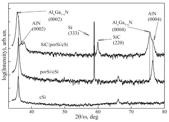
Figure 4.
X-ray ω/2θ for diffraction of the samples of AlxGa1-xN/AlN heterostructures grown on different substrates.
As for the diffraction from the epitaxial AlxGa1-xN/AlN film, its intensity is 3–4 orders of magnitude lower than that of the Si substrate, and this fact indicates a small thickness of the epitaxial layer. According to the experimental results, maxima near 36.05°, 37.9°, 66.11° and 76.5° can be observed in the diffraction patterns of all AlxGa1-xN/AlN heterostructures, which are attributed to the reflections from the (0002), (), () and (0004) planes of wurtzite AlN. The reflections of 0002 and 0004 are most intensive in the set of these peaks, and this means that AlN columns are preferably grown in the <0001> direction for all three samples. However, the presence of additional low-intensive reflections () and () in the diffraction patterns indicates misorientation of the AlN nanocolumns relative to the growth direction, specified by the (111) orientation of the Si substrate as the probable silting of AlN nanocolumns in the directions of <> and <>.
It should be noted that the reflection near 35.8° can be observed only in the diffraction pattern of the sample grown on the SiC/porSi/cSi substrate, which can be correctly attributed to (0002) reflection from AlxGa1-xN alloy. Moreover, in the ω/2θ diffraction pattern of the SiC/porSi/cSi sample, one can see a diffraction peak attributed to the cubical polytype of SiC-3C, as shown in [22], irrespective of Si crystal orientation, Si treatment or the formation of pores in Si. Due to the features of the mechanism regarded with matched substitution of the atoms (see [11]), (111) SiC faces are always formed on the Si surface. At the boundaries of pores and the (111) Si surface, (111) SiC faces can be inclined or rotated relative to the (111) Si face.
It should be noted that the absence of reflections from AlxGa1-xN in the diffraction patterns of the samples on the cSi and porSi/cSi substrates is caused by different efficiencies in the incorporation of Ga atoms under epitaxial synthesis of AlxGa1-xN alloys on the nanocolumnar buffer layer of AlN grown on the silicon substrate without a SiC layer and with this layer. The differences in thickness of AlxGa1-xN/AlN heterostructures observed in the SEM images can be proof of the formation of Ga-enriched clusters, where there is no long-range order in their crystal structure. This probably results in a smearing of diffraction peaks of AlxGa1-xN for the structures grown on cSi and porSi/cSi.
Based on the data of X-ray diffraction, the lattice parameters for the epitaxial AlN layer and AlxGa1-xN alloy were calculated. In accordance with anisotropic theory of elasticity for the epitaxial layers with wurtzite lattice, the in-plane deformation (along the a axis) and out-of-plane deformation (along the c axis) were determined, as well as the in-plane biaxial stress in the growth plane [23]. It is assumed that for the calculation of the crystal lattice parameters as well as the coefficients of elastic deformations C(x)ij for the alloys, the use of Poisson–Vegard law is valid [24,25,26,27].
The calculated values of the crystal lattice parameters, components of the in-plane elastic deformation and the growth direction , as well as the in-plane stresses for the growth plane for the epitaxial layers of the investigated samples, are presented in Table 2.
Table 2.
Results of X-ray diffraction.
In our calculations, we used the value of the concentration magnitude of the Al atoms in the AlxGa1-xN alloy determined using the XPS technique (see Table 1). Moreover, when performing the calculations, the following values for the parameters were used from the literature: , [28,29], , [28,29], = 106 GPa, = 390 GPa [29], = 145 GPa [23], = 99 Gpa, = 389 GPa [29] and = 149 GPa [30].
The obtained results show that deformations in the AlN layers and AlxGa1-xN alloys are of a different sign. They prove to be tensile strains in the growth plane, while they appear to be compressive strains in the growth direction. This happens due to the mismatch in the crystal lattice parameters between the substrate and epitaxial layers of AlN and AlxGa1-xN. It should be noted that the lowest level of residual stresses for the AlN layer is observed in the sample formed on the hybrid SiC/porSi/cSi substrate. However, in the layer of AlxGa1-xN alloy for the heterostructure grown on the SiC/porSi/cSi substrate, the level of residual stresses is an order of magnitude higher than the one observed in the AlN sublayer.
The crystal quality of the grown AlxGa1-xN/AlN heterostructures was characterized using the measurements of the X-ray rocking curves. The ω-diffraction curves near the site of (0002) AlN are presented in Figure 5.
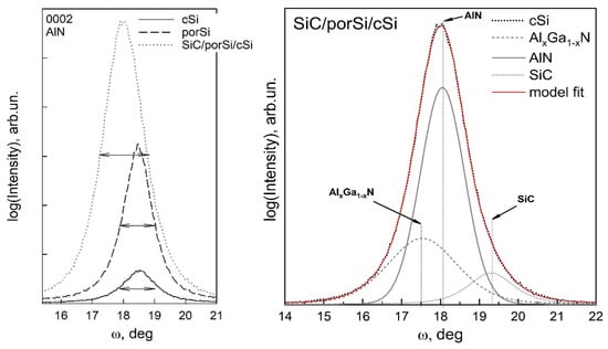
Figure 5.
X-ray ω-rocking curves near the plane of 0002 AlN for the cSi, porSi/cSi and SiC/porSi/cSi samples (left). Deconvolution of the rocking curve near the plane of 0002 AlN for the SiC/porSi/cSi sample (right).
A preliminary analysis of ω-rocking curves (see Figure 5) showed that the profile of the curve for the heterostructure grown on the SiC/porSi/cSi substrate is quite noticeably asymmetric. Based on the ω/2θ scanning data, this fact is connected with the superposition of reflections from different layers of the heterostructure. In order to determine the contribution of each of the maximums, we performed a deconvolution of the line profiles into the components (see Figure 5, right). The simulation of the profile was performed in OriginPro 2018 software. The determination of the number of extremes was realized with the use of a second derivative. One can clearly see that the shape of the profile is caused by the superposition of the line from the AlN layer and AlxGa1-xN alloy, as well as from the low-intensive maximum arranged at the large diffraction angles. This reflection is attributed to the cubic 3C-SiC, keeping in mind that its lattice is characterized by tetragonal distortions due to mismatches in the parameters of crystal lattices.
Since the angular width of the reflection in the ω-rocking curve correlates with the mosaic structure of the crystallites (rotation angle) relative to each other, the angular range of the crystallite misorientation in the epitaxial film can be estimated as the difference in the width of the layer rocking curve and the instrumental width of the line . Here, the width of the 004 reflection in the reference silicon sample NIST SRM degrees was taken as the instrumental width, and it was measured in similar conditions.
Our results show that crystal mosaic structure for the AlN layer is ±0.62°, ±0.55° and ±0.67° for the samples grown on the cSi, SiC/cSi and SiC/porSi/cSi substrates. It is clearly seen that less dispersion of mosaic structure is characteristic for a nanocolumnar epitaxial structure grown on a porSi/cSi substrate, which was previously observed in our works [15,31] but for thick layers. At the same time, the characteristic value of the mosaic structure for nanocrystals of AlxGa1-xN alloy grown on SiC/porSi/cSi substrate is ±1.02. An increase in the FWHM of the X-ray ω-rocking curve can be explained by the inclination of the nanocolumns due to the relaxation of stresses caused by mismatches in the lattice parameters for the epitaxial layer and substrate.
The optical properties of AlxGa1-xN/AlN heterostructures in the UV wavelength range were studied based on our elaborated technique [32]. To realize these investigations, the transmission–reflection spectra were obtained within the range of 1–6 eV. The obtained data were used to calculate the optical density D. After that, the (D·hν)2 dependences on hν were plotted and then their graphical analysis was completed with the use of the Tautz technique [33]. As a result, the parts of the spectra with a linear dependence on (D·hν)2 were found, indicating the presence of direct allowed transitions in this spectral range. The energy of these transitions was compared with the known literature data for similar samples.
From the obtained results (see Figure 6), it follows that for all of the studied samples, the appearance of two direct transitions with energies in the range of 3.2–3.6 eV and 4.1–4.4 eV takes place. At the same time, in the spectra of the heterostructure grown on the SiC/porSi/cSi substrate, one more transition in the range of lower energies ~2.5 eV (Figure 6, right) was detected using the Tautz technique.
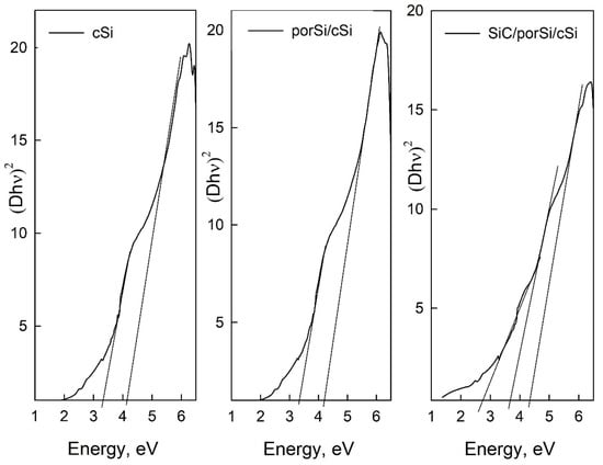
Figure 6.
Graphical analysis of (D·hν)2 dependences on the energy of optical emission using the Tautz method for AlxGa1-xN/AlN heterostructures, grown on the cSi (left), porSi/cSi (central) and SiC/porSi/cSi (right) substrates.
The observed high-energy transition can be attributed to the direct allowed interband transition of band-to-band type in the Γ point of the Brillouin zone in wurtzite AlN and so coinciding with the energy of the band gap.
A number of studies in the literature specify that the value of the band gap in Al, is Eg~6 eV. However, many times previously, a narrowing band gap up to the value of Eg~4.1 eV in the films of aluminum nitride grown at reduced values of the substrate temperature [34] was demonstrated. In some other works, the value of Eg~5.1 eV was demonstrated for films of AlN grown on Si(100) substrates for different temperatures of the substrate: from room temperature (RT) to 500 °C [35]. Narrowing of the band gap in AlN up to the value of Eg~4.6 eV was also observed in the films of high-textured aluminum nitride [36]. The second transition of about 3.2–3.6 eV, detected in all the structures, is probably attributed to the high density of defects in the material, which form energy levels in the band gap and tails in the density of states in the valence and conduction bands.
As for the direct transition at ~2.5 eV found in the sample grown on the SiC/porSi/cSi substrate, this absorption band coincides quite well with the energy of the band gap in the cubic polytype of silicon carbide 3C-SiC, Eg (Γ15v-X1c)~2.41 eV [37]. Note, that in [38], it is mentioned that deformations appearing in the thin layers can cause rather large (up to 0.5 eV) shifts in the value of the optical width of the band gap. Taking into account the fact that the error in the used method of the study of optical properties is of ~0.1–0.2 eV, experimentally found direct transitions in the range of 3.95–4.15 eV can probably be attributed to the optical absorption in the AlxGa1-xN alloy.
One should note that the experimentally detected shifts in the energy of direct transitions for GaN correlate with the value of in-plane biaxial stress calculated based on X-ray diffractometry data.
The photoluminescence spectra of the epitaxial AlxGa1-xN/AlN heterostructures for all the studied samples are presented in Figure 7. It is readily seen that luminescence of the samples in the range of 300–900 nm depends on the type of substrate used for the growth process.
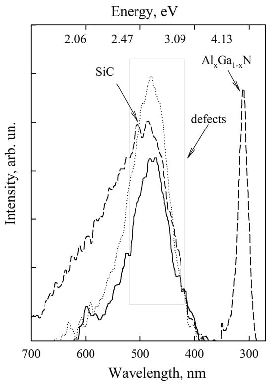
Figure 7.
PL spectra at T~300 C for AlxGa1-xN/AlN heterostructures grown on the cSi, porSi/cSi and SiC/porSi/cSi substrates.
The performed investigations show that a high-energy peak with the energy of its maximum Eg = 3.99 eV, i.e., in UV spectral range near 310 nm, is observed only in the PL spectrum of the AlxGa1-xN/AlN heterostructure grown on the SiC/porSi/cSi substrate. Moreover, in all the spectra, an additional broad yellow spectral band can be observed. It is attributed to the spurious defect that appeared due to the high density of defects in the material, which form energy levels in the band gap and tails in the density of states of the valence band and conduction band [39]. This result correlates fairly well with the dataf form the XPS analysis. One should note that in the experimental spectrum of the film obtained on the hybrid SiC/porSi/cSi substrate, the peak is present near 2.34 eV. This maximum can be attributed to the 3C-SiC sublayer, with the energy value of the band- gap approximately equal to Eg ~2.24–2.39 eV [40,41], which also correlates with our results obtained using the UV technique.
The value of the optical width of the band gap is known to be used for the estimation of the composition of the AlxGa1-xN alloy [42]
According to Vegard’s law, the dependence of the band gap value in the AlxGa1-xN alloy on the content of Al is of a non-linear character:
where b is a bending parameter.
= 3.45 eV, = 6.13 eV and b~1.0 ± 0.3 at room temperature. However, as shown in [43], at x ≤ 0.25, one can neglect the last term in (1); therefore, this dependence can be regarded as linear.
Considering these assumptions for the heterostructure grown on the SiC/porSi/cSi substrate, the composition of the Al0.20Ga0.80N alloy was determined, which is in good accordance with the results of photoelectron microscopy. The fact that one cannot observe UV PL in the samples grown on the porSi/cSi and cSi substrates correlates with the results of X-ray diffraction. This indicates the absence of the formed Al0.20Ga0.80N alloy in these samples.
4. Conclusions
Combining the methods of structural, microscopy and spectroscopic diagnostics in our work, we performed comparative studies of nanoscale columnar AlxGa1-xN/AlN heterostructures synthesized on cSi, porSi/cSi and SiC/porSi/cSi substrates using the MBE PA technique.
As it follows from the experimental data, the composition, thickness and morphology of the deposited film as well as the aluminum content in AlxGa1-xN alloy depend on the type of substrates used in this work. The AlxGa1-xN layer with a composition of x~0.20 was formed only on the hybrid SiC/porSi/cSi substrate, while the AlxGa1-xN layer on the substrates of cSi and porSi/cSi was not formed in effect. It was found that the epitaxial growth of AlxGa1-xN heterostructures in N-enriched conditions resulted in the formation of AlxGa1-xN/AlN layers with a Ga-polar surface.
The analysis of microscopy data also confirms the formation of a layer with nanocolumnar morphology; the lateral size of the grains (nanocolumns) varies in a wide range from several dozen up to a hundred nanometers. The formed nanocolumns of AlxGa1-xN are inclined relative to the c-axis, which is probably caused by the relaxation of elastic stresses due to the mismatch in the lattice parameters between the epitaxial layer and substrate.
As for the optical properties of the samples presented as AlxGa1-xN/AlN heterostructures in the range of 1–6 eV, their optical absorption/luminescence also depends on the type of substrate used for heterostructure growth. It is shown that in he PL spectrum of only the AlxGa1-xN/AlN heterostructure grown on the SiC/porSi/cSi substrate, a high-energy peak with an energy corresponding Eg = 3.99 eV is observed, corresponding to the value of the band gap in the AlxGa1-xN (x~0.20) alloy. In the spectra of all the investigated samples, one can observe a yellow photoluminescence band, which is usually attributed to the presence of deep defects in the band gap of AIIIN layers [44].
Thus, our investigations showed that with the use of one and the same conditions in the MBE PA process, the AlxGa1-xN(x~0.20)/AlN heterostructure with nanocolumnar morphology quite successfully grows on the hybrid SiC/porSi/cSi substrate, while the AlxGa1-xN layer with x < 0.07 grown on the cSi and porSi/cSi layers is present only at the stage of disordered alloy.
While discussing the efficiency of the use of hybrid substrates instead of single-crystalline ones, it should be noted that the known attempts at growth on hybrid substrates, including those with porous layers, have repeatedly shown the prospects of such an approach to the formation of the integrated AIIIBV/Si nano-heterostructures [45,46,47,48]. Structuring of the hybrid compliant substrate as well as the growth of nanoscale layers with nanocolumnar morphology propose some additional advantages for the integration.
The obtained results unambiguously indicate the different mechanisms underlying the growth of AlxGa1-xN films on the nanocolumnar AlN buffer layer obtained on silicon substrates without the SiC layer and with this layer. The presence of the SiC layer in the template composition, grown in porous Si, quite efficiently influences the growth mechanisms of the films and their adsorption characteristics, increasing the nucleation rate of the ordered AlxGa1-xN alloy with a specified composition and, hence, has an effect on the structural and optical quality of AIIIN structures.
The results presented in this work demonstrate the availability of the use of SiC/porSi/cSi substrates for the integration of silicon technology and technology for the synthesis of nanoscale columnar AlxGa1-xN using molecular-beam epitaxy with plasma-activated nitrogen.
Author Contributions
Conceptualization, P.V.S., D.L.G., S.A.K. and A.M.; methodology, P.V.S., D.L.G., S.A.K. and A.M.; validation, P.V.S., D.L.G., S.A.K., and A.M.; formal analysis, P.V.S., D.L.G., S.A.K. and A.M.; investigation, N.K., V.K., A.S.L., N.B., D.N., S.A.K., S.T., K.Y.S. and M.S.S.; resources, P.V.S.; data curation, P.V.S., D.L.G., S.A.K. and A.M.; writing—original draft preparation, P.V.S., N.K., D.L.G., S.A.K. and A.M.; writing—review and editing, P.V.S., N.K., D.L.G., S.A.K. and A.M.; visualization, D.L.G., N.B. and D.N.; supervision, P.V.S.; project administration, P.V.S.; funding acquisition, P.V.S. All authors have read and agreed to the published version of the manuscript.
Funding
This work was carried out under the financial support of the Russian Science Foundation, grant 19-72-10007. Adjustment of the formation of the hybrid substrate was performed under the support of the Ministry of Science and Higher Education of Russia (grant No. FZGU-2023-0006). Synthesis of the samples using the MBE PA technique, as well as the study of heterostructures polarity were completed under the support of the Ministry of Science and Higher Education of Russia No. FSRM-2023-0006. As for access to scientific equipment and methodology of measurements and analysis, this study was carried out under the support of the Ministry of Science and Higher Education of Russia, contract No. 075-15-2021-1351.
Data Availability Statement
Data are available on request.
Conflicts of Interest
The authors declare no conflict of interest.
References
- Zou, C.; Zhao, Z.; Xu, M.; Wang, X.; Liu, Q.; Chen, K.; He, L.; Gao, F.; Li, S. GaN/Gr (2D)/Si (3D) Combined High-Performance Hot Electron Transistors. ACS Nano 2023, 17, 8262–8270. [Google Scholar] [CrossRef] [PubMed]
- Das, P.; Wu, T.-L.; Tallur, S. Design and Analysis of High Electron Mobility Transistor Inspired: III-V Electro-Optic Modulator Topologies. Semicond. Sci. Technol. 2020, 35, 095028. [Google Scholar] [CrossRef]
- Kohen, D.; Nguyen, X.S.; Yadav, S.; Kumar, A.; Made, R.I.; Heidelberger, C.; Gong, X.; Lee, K.H.; Lee, K.E.K.; Yeo, Y.C.; et al. Heteroepitaxial Growth of In0.30Ga0.70As High-Electron Mobility Transistor on 200 Mm Silicon Substrate Using Metamorphic Graded Buffer. AIP Adv. 2016, 6, 085106. [Google Scholar] [CrossRef]
- Du, H.; Liu, Z.; Hao, L.; Su, H.; Zhang, T.; Zhang, W.; Zhang, J.; Hao, Y. High-Performance E-Mode p-Channel GaN FinFET on Silicon Substrate with High ION/IOFF and High Threshold Voltage. IEEE Electron Device Lett. 2022, 43, 705–708. [Google Scholar] [CrossRef]
- Del Alamo, J.A.; Antoniadis, D.A.; Lin, J.; Lu, W.; Vardi, A.; Zhao, X. Nanometer-Scale III-V MOSFETs. IEEE J. Electron Devices Soc. 2016, 4, 205–214. [Google Scholar] [CrossRef]
- Riel, H.; Wernersson, L.-E.; Hong, M.; del Alamo, J.A. III–V Compound Semiconductor Transistors—From Planar to Nanowire Structures. MRS Bull. 2014, 39, 668–677. [Google Scholar] [CrossRef]
- Horta, I.M.; Damasceno, B.S.; De Oliveira, R.S.; Pereira, A.L.D.J.; Massi, M.; Sobrinho, A.S.D.S.; Leite, D.M.G. AlGaN Films Grown by Reactive Magnetron Sputtering on Glass Substrates with Different Al Content. Surf. Interfaces 2023, 40, 103023. [Google Scholar] [CrossRef]
- del Alamo, J.A. Nanometre-Scale Electronics with III–V Compound Semiconductors. Nature 2011, 479, 317–323. [Google Scholar] [CrossRef]
- Wang, Z.; Abbasi, A.; Dave, U.; De Groote, A.; Kumari, S.; Kunert, B.; Merckling, C.; Pantouvaki, M.; Shi, Y.; Tian, B.; et al. Novel Light Source Integration Approaches for Silicon Photonics: Novel Light Source Integration Approaches for Silicon Photonics. Laser Photonics Rev. 2017, 11, 1700063. [Google Scholar] [CrossRef]
- Chen, K.; Wang, X.; Zou, C.; Liu, Q.; Chen, K.; Shi, Y.; Xu, T.; Zhao, W.; He, L.; Gao, F.; et al. Two-In-One: End-Emitting Blue LED and Self-Powered UV Photodetector Based on Single Trapezoidal PIN GaN Microwire for Ambient Light UV Monitoring and Feedback. Small Methods 2023, 7, 2300138. [Google Scholar] [CrossRef]
- Wang, H.-C.; Tang, T.-Y.; Yang, C.C.; Malinauskas, T.; Jarasiunas, K. Carrier Dynamics in Coalescence Overgrowth of GaN Nanocolumns. Thin Solid Films 2010, 519, 863–867. [Google Scholar] [CrossRef]
- Lu, J.; Zheng, X.; Guidry, M.; Denninghoff, D.; Ahmadi, E.; Lal, S.; Keller, S.; DenBaars, S.P.; Mishra, U.K. Engineering the (In, Al, Ga)N Back-Barrier to Achieve High Channel-Conductivity for Extremely Scaled Channel-Thicknesses in N-Polar GaN High-Electron-Mobility-Transistors. Appl. Phys. Lett. 2014, 104, 092107. [Google Scholar] [CrossRef]
- Keller, S.; Fichtenbaum, N.A.; Furukawa, M.; Speck, J.S.; DenBaars, S.P.; Mishra, U.K. Growth and Characterization of N-Polar InGaN∕GaN Multiquantum Wells. Appl. Phys. Lett. 2007, 90, 191908. [Google Scholar] [CrossRef]
- Wu, Y.; Liu, X.; Pandey, A.; Zhou, P.; Dong, W.J.; Wang, P.; Min, J.; Deotare, P.; Kira, M.; Kioupakis, E.; et al. III-Nitride Nanostructures: Emerging Applications for Micro-LEDs, Ultraviolet Photonics, Quantum Optoelectronics, and Artificial Photosynthesis. Prog. Quantum Electron. 2022, 85, 100401. [Google Scholar] [CrossRef]
- Seredin, P.V.; Leiste, H.; Lenshin, A.S.; Mizerov, A.M. Effect of the Transition Porous Silicon Layer on the Properties of Hybrid GaN/SiC/Por-Si/Si(111) Heterostructures. Appl. Surf. Sci. 2020, 508, 145267. [Google Scholar] [CrossRef]
- Ghosh, P.K.; Sarollahi, M.; Li, C.; White, T.; Debu, D.T.; Yan, Q.; Kuchuk, A.; Kumar, R.; Shetty, S.; Salamo, G.J.; et al. High Temperature Capacitors Using AlN Grown by MBE as the Dielectric. J. Vac. Sci. Technol. B 2018, 36, 041202. [Google Scholar] [CrossRef]
- Shih, H.-J.; Lo, I.; Wang, Y.-C.; Tsai, C.-D.; Lin, Y.-C.; Lu, Y.-Y.; Huang, H.-C. Growth and Characterization of GaN/InxGa1−xN/InyAl1−yN Quantum Wells by Plasma-Assisted Molecular Beam Epitaxy. Crystals 2022, 12, 417. [Google Scholar] [CrossRef]
- Yamabe, N.; Shimomura, H.; Shimamura, T.; Ohachi, T. Nitridation of Si(111) for Growth of 2H-AlN(0001)/β-Si3N4 /Si(111) Structure. J. Cryst. Growth 2009, 311, 3049–3053. [Google Scholar] [CrossRef]
- Yamabe, N.; Yamamoto, Y.; Ohachi, T. Epitaxial Growth of β-Si3N4 by the Nitridation of Si with Adsorbed N Atoms for Interface Reaction Epitaxy of Double Buffer AlN(0001)/β-Si3N4/Si(111). Phys. Status Solidi C 2011, 8, 1552–1555. [Google Scholar] [CrossRef]
- Moulder, J.F.; Chastain, J. (Eds.) Handbook of X-ray Photoelectron Spectroscopy: A Reference Book of Standard Spectra for Identification and Interpretation of XPS Data; Perkin-Elmer Corporation: Eden Prairie, MN, USA, 1992; ISBN 978-0-9627026-2-4. [Google Scholar]
- New Semiconductor Materials. Biology Systems. Characteristics and Properties; Ioffe Institute: Saint Petersburg, Russia, 2007. [Google Scholar]
- Kidalov, V.V.; Kukushkin, S.A.; Osipov, A.; Redkov, A.; Grashchenko, A.S.; Soshnikov, I.P. Growth of Sic Films by the Method of Substitution of Atoms on Porous Si (100) and (111) Substrates. Mater. Phys. Mech. 2018, 36, 39–52. [Google Scholar] [CrossRef]
- Harutyunyan, V.S.; Aivazyan, A.P.; Weber, E.R.; Kim, Y.; Park, Y.; Subramanya, S.G. High-Resolution X-ray Diffraction Strain-Stress Analysis of GaN/Sapphire Heterostructures. J. Phys. Appl. Phys. 2001, 34, A35–A39. [Google Scholar] [CrossRef]
- Lee, H.-P.; Perozek, J.; Rosario, L.D.; Bayram, C. Investigation of AlGaN/GaN High Electron Mobility Transistor Structures on 200-Mm Silicon (111) Substrates Employing Different Buffer Layer Configurations. Sci. Rep. 2016, 6, 37588. [Google Scholar] [CrossRef]
- Jana, S.K.; Mukhopadhyay, P.; Ghosh, S.; Kabi, S.; Bag, A.; Kumar, R.; Biswas, D. High-Resolution X-ray Diffraction Analysis of AlxGa1−xN/InxGa1−xN/GaN on Sapphire Multilayer Structures: Theoretical, Simulations, and Experimental Observations. J. Appl. Phys. 2014, 115, 174507. [Google Scholar] [CrossRef]
- Seredin, P.V.; Glotov, A.V.; Domashevskaya, E.P.; Arsentyev, I.N.; Vinokurov, D.A.; Tarasov, I.S. Structural Features and Surface Morphology of AlxGayIn1-x-yAszP1-z/GaAs(100) Heterostructures. Appl. Surf. Sci. 2013, 267, 181–184. [Google Scholar] [CrossRef]
- Seredin, P.V.; Glotov, A.V.; Ternovaya, V.E.; Domashevskaya, E.P.; Arsentyev, I.N.; Vavilova, L.S.; Tarasov, I.S. Spinodal Decomposition of GaxIn1−xAsyP1−y Quaternary Alloys. Semiconductors 2011, 45, 1433–1440. [Google Scholar] [CrossRef]
- Morkoç, H. Handbook of Nitride Semiconductors and Devices: Materials Properties, Physics and Growth, 1st ed.; Wiley: Hoboken, NJ, USA, 2008; ISBN 978-3-527-40837-5. [Google Scholar]
- Madelung, O.; Rössler, U.; Schulz, M. (Eds.) III/17A-22A-41A1a List of Frequently Used Symbols and Abbreviations, Conversion Factors. In Group IV Elements, IV–IV and III-V Compounds. Part A—Lattice Properties; Springer: Berlin/Heidelberg, Germany, 2001; Volume a, pp. 1–7. ISBN 978-3-540-64070-7. [Google Scholar]
- Dai, Y.; Li, S.; Sun, Q.; Peng, Q.; Gui, C.; Zhou, Y.; Liu, S. Properties of AlN Film Grown on Si (111). J. Cryst. Growth 2016, 435, 76–83. [Google Scholar] [CrossRef]
- Seredin, P.V.; Leiste, H.; Lenshin, A.S.; Mizerov, A.M. HRXRD Study of the Effect of a Nanoporous Silicon Layer on the Epitaxial Growth Quality of GaN Layer on the Templates of SiC/Por-Si/c-Si. Results Phys. 2020, 16, 102919. [Google Scholar] [CrossRef]
- Seredin, P.V.; Lenshin, A.S.; Zolotukhin, D.S.; Arsentyev, I.N.; Nikolaev, D.N.; Zhabotinskiy, A.V. Experimental Study of Structural and Optical Properties of Integrated MOCVD GaAs/Si(001) Heterostructures. Phys. B Condens. Matter 2018, 530, 30–37. [Google Scholar] [CrossRef]
- Tauc, J. Optical Properties of Semiconductors in the Visible and Ultra-Violet Ranges. Prog. Semicond. Heywood Lond. 1965, 9, 87–133. [Google Scholar]
- Bakalova, S.; Szekeres, A.; Anastasescu, M.; Gartner, M.; Duta, L.; Socol, G.; Ristoscu, C.; Mihailescu, I.N. VIS/IR Spectroscopy of Thin AlN Films Grown by Pulsed Laserdeposition at 400 °C and 800 °C and Various N2 Pressures. J. Phys. Conf. Ser. 2014, 514, 012001. [Google Scholar] [CrossRef]
- Sharma, N.; Sharma, S.; Prabakar, K.; Amirthapandian, S.; Ilango, S.; Dash, S.; Tyagi, A.K. Optical Band Gap and Associated Band-Tails in Nanocrystalline AlN Thin Films Grown by Reactive IBSD at Different Substrate Temperatures. arXiv 2015, arXiv:1507.04867. [Google Scholar] [CrossRef]
- Frontiers | Measurement and Ab Initio Investigation of Structural, Electronic, Optical, and Mechanical Properties of Sputtered Aluminum Nitride Thin Films. Available online: https://www.frontiersin.org/articles/10.3389/fphy.2020.00115/full (accessed on 25 October 2022).
- Lee, K.M.; Hwang, J.Y.; Urban, B.; Singh, A.; Neogi, A.; Lee, S.K.; Choi, T.Y. Origin of Broad Band Emissions of 3C-Silicon Carbide Nanowire by Temperature and Time Resolved Photoluminence Study. Solid State Commun. 2015, 204, 16–18. [Google Scholar] [CrossRef]
- Shan, W.; Ager, J.W.; Yu, K.M.; Walukiewicz, W.; Haller, E.E.; Martin, M.C.; McKinney, W.R.; Yang, W. Dependence of the Fundamental Band Gap of AlxGa1−xN on Alloy Composition and Pressure. J. Appl. Phys. 1999, 85, 8505–8507. [Google Scholar] [CrossRef]
- Serban, E.; Palisaitis, J.; Junaid, M.; Tengdelius, L.; Högberg, H.; Hultman, L.; Persson, P.; Birch, J.; Hsiao, C.-L. Magnetron Sputter Epitaxy of High-Quality GaN Nanorods on Functional and Cost-Effective Templates/Substrates. Energies 2017, 10, 1322. [Google Scholar] [CrossRef]
- Zhao, G.L.; Bagayoko, D. Electronic Structure and Charge Transfer in 3C- and 4H-SiC. New J. Phys. 2000, 2, 16. [Google Scholar] [CrossRef]
- Physical Parameterisation of 3C-Silicon Carbide (SiC) with Scope to Evaluate the Suitability of the Material for Power Diodes as an Alternative to 4H-SiC | IEEE Conference Publication | IEEE Xplore. Available online: https://ieeexplore.ieee.org/document/8062411 (accessed on 24 October 2022).
- Aggarwal, N.; Krishna, S.; Goswami, L.; Jain, S.K.; Pandey, A.; Gundimeda, A.; Vashishtha, P.; Singh, J.; Singh, S.; Gupta, G. Investigating the Growth of AlGaN/AlN Heterostructure by Modulating the Substrate Temperature of AlN Buffer Layer. SN Appl. Sci. 2021, 3, 291. [Google Scholar] [CrossRef]
- Angerer, H.; Brunner, D.; Freudenberg, F.; Ambacher, O.; Stutzmann, M.; Höpler, R.; Metzger, T.; Born, E.; Dollinger, G.; Bergmaier, A.; et al. Determination of the Al Mole Fraction and the Band Gap Bowing of Epitaxial AlxGa1−xN Films. Appl. Phys. Lett. 1997, 71, 1504–1506. [Google Scholar] [CrossRef]
- Turkulets, Y.; Shauloff, N.; Chaulker, O.H.; Shapira, Y.; Jelinek, R.; Shalish, I. The GaN(0001) Yellow-Luminescence-Related Surface State and Its Interaction with Air. Surf. Interfaces 2023, 38, 102834. [Google Scholar] [CrossRef]
- Boufaden, T.; Chaaben, N.; Christophersen, M.; El Jani, B. GaN Growth on Porous Silicon by MOVPE. Microelectron. J. 2003, 34, 843–848. [Google Scholar] [CrossRef]
- Ishikawa, H.; Shimanaka, K.; Azfar bin, M.; Amir, M.; Hara, Y.; Nakanishi, M. Improved MOCVD Growth of GaN on Si-on-Porous-Silicon Substrates. Phys. Status Solidi C 2010, 7, 2049–2051. [Google Scholar] [CrossRef]
- Gommé, G.; Gautier, G.; Portail, M.; Frayssinet, E.; Alquier, D.; Cordier, Y.; Semond, F. A Detailed Study of AlN and GaN Grown on Silicon-on-Porous Silicon Substrate: AlN and GaN Grown on Silicon-on-Porous Silicon Substrate. Phys. Status Solidi A 2017, 214, 1600450. [Google Scholar] [CrossRef]
- Abud, S.H.; Selman, A.M.; Hassan, Z. Investigation of Structural and Optical Properties of GaN on Flat and Porous Silicon. Superlattices Microstruct. 2016, 97, 586–590. [Google Scholar] [CrossRef]
Disclaimer/Publisher’s Note: The statements, opinions and data contained in all publications are solely those of the individual author(s) and contributor(s) and not of MDPI and/or the editor(s). MDPI and/or the editor(s) disclaim responsibility for any injury to people or property resulting from any ideas, methods, instructions or products referred to in the content. |
© 2023 by the authors. Licensee MDPI, Basel, Switzerland. This article is an open access article distributed under the terms and conditions of the Creative Commons Attribution (CC BY) license (https://creativecommons.org/licenses/by/4.0/).