
Fabrication Process for On-Board Geometries Using a Polymer Composite-Based Selective Metallization for Next-Generation Electronics Packaging


Abstract
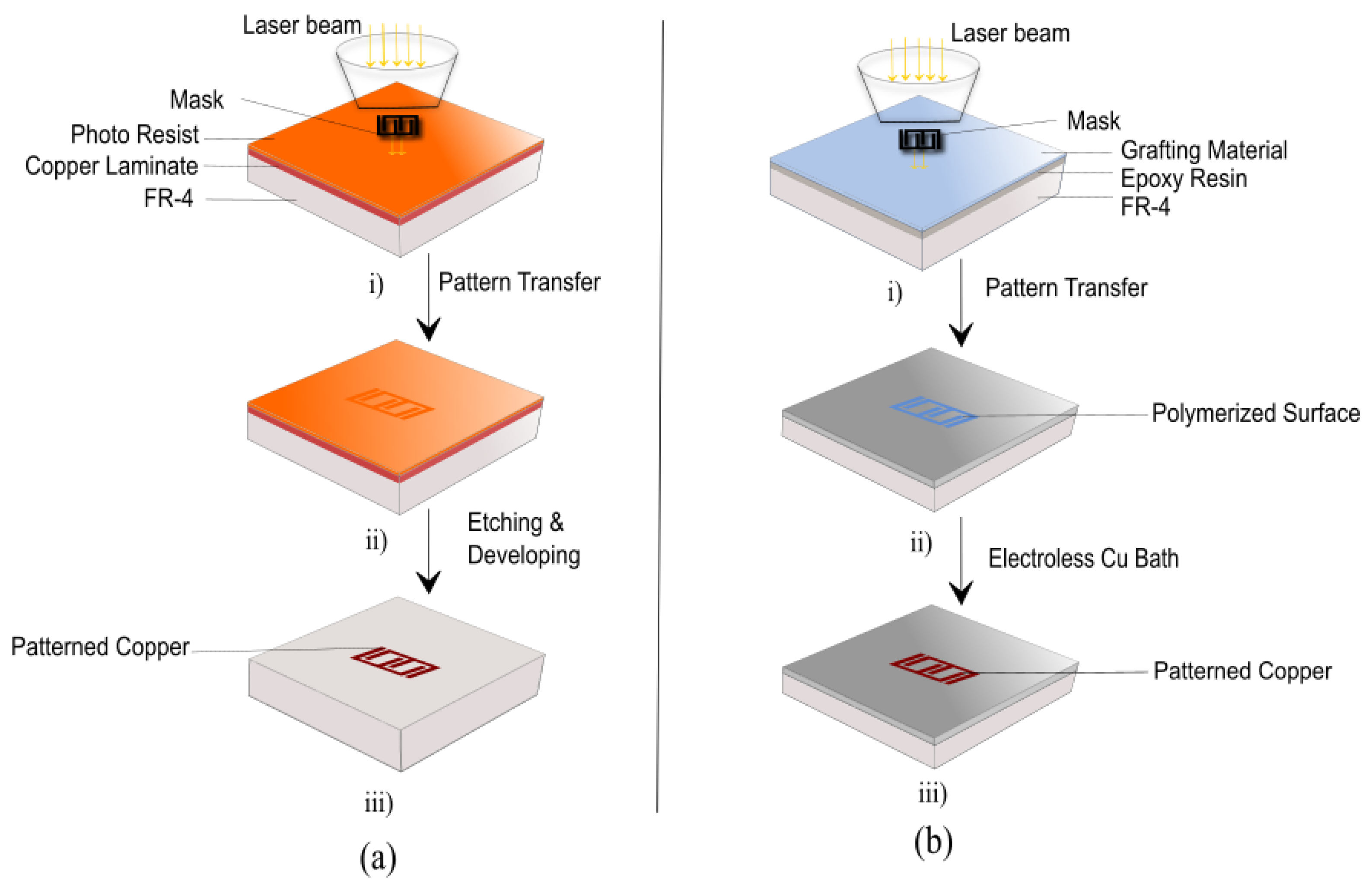
:1. Introduction
- To demonstrate a fully additive process using exopy resins and polymer-based CBM technology to procure any desirable geometries on the FR-4 substrate.
- To show the selective metallization capability of the process by eliminating the etching process significantly (especially during the metallization), i.e., adapting an environmentally friendlier production approach.
- To present the feasibility of the fabrication technique at lower temperature (20–45 °C).
- To show the possibility of process implementation for the PCB fabrication segment of the industry towards miniaturization.
2. Materials and Methods
2.1. Sample Preparation
2.2. Fabrication Steps
- Step 1:
- Ultrasonic cleaning of the FR-4 substrate using deionized water (DIW).
- Step 2:
- Drying of the FR-4 substrate at room temperature.
- Step 3:
- Spin coating of the PU layer on top of FR-4.
- Step 4:
- UV soft baking for 1 min followed by surface hardening at room temperature.
- Step 5:
- Spin coating of HP-14 on PU.
- Step 6:
- Selective polymerization of the surface using actinic radiation and pattern file (optional in case of bulk Cu deposition).
- Step 7:
- Proper cleaning using DIW of the sample to remove the unexposed HP-14 solution from the sample surface before the Cu bath.
- Step 8:
- Electroless Cu bath (Predip, Activator, Reducer and Cu bath).
- Step 9:
- Final cleaning of the surface and characterization.
2.3. Characterization
3. Results and Discussion
3.1. Surface Mechanism of the Polymerization
3.1.1. Selective Polymerization with Patterns
3.1.2. Selective Metallization
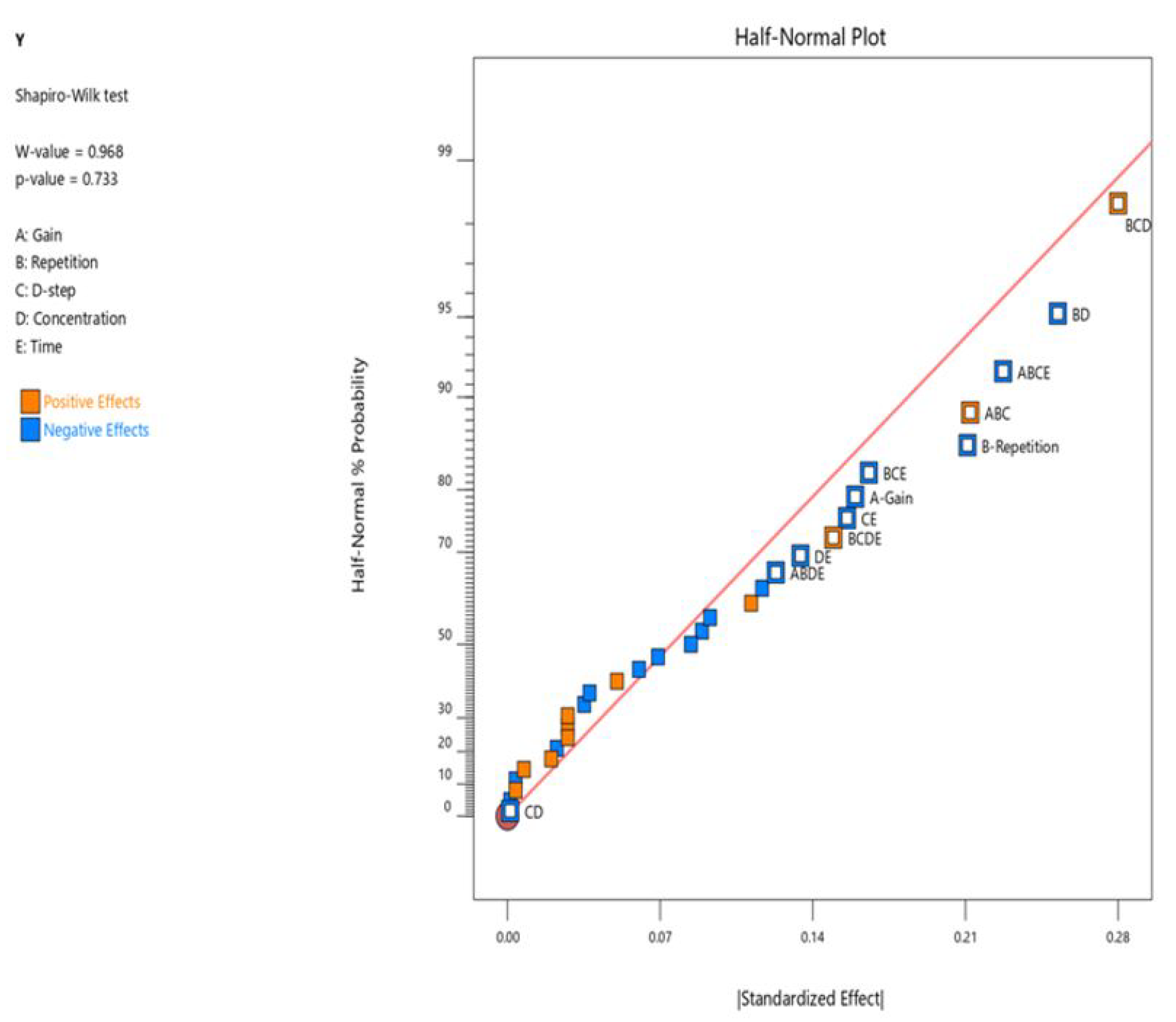
3.2. Parameter Optimization
Significance Level of Parameters
3.3. Challenges in Fabrication
3.3.1. Inadequate Laser Exposure
3.3.2. Improper Metallization
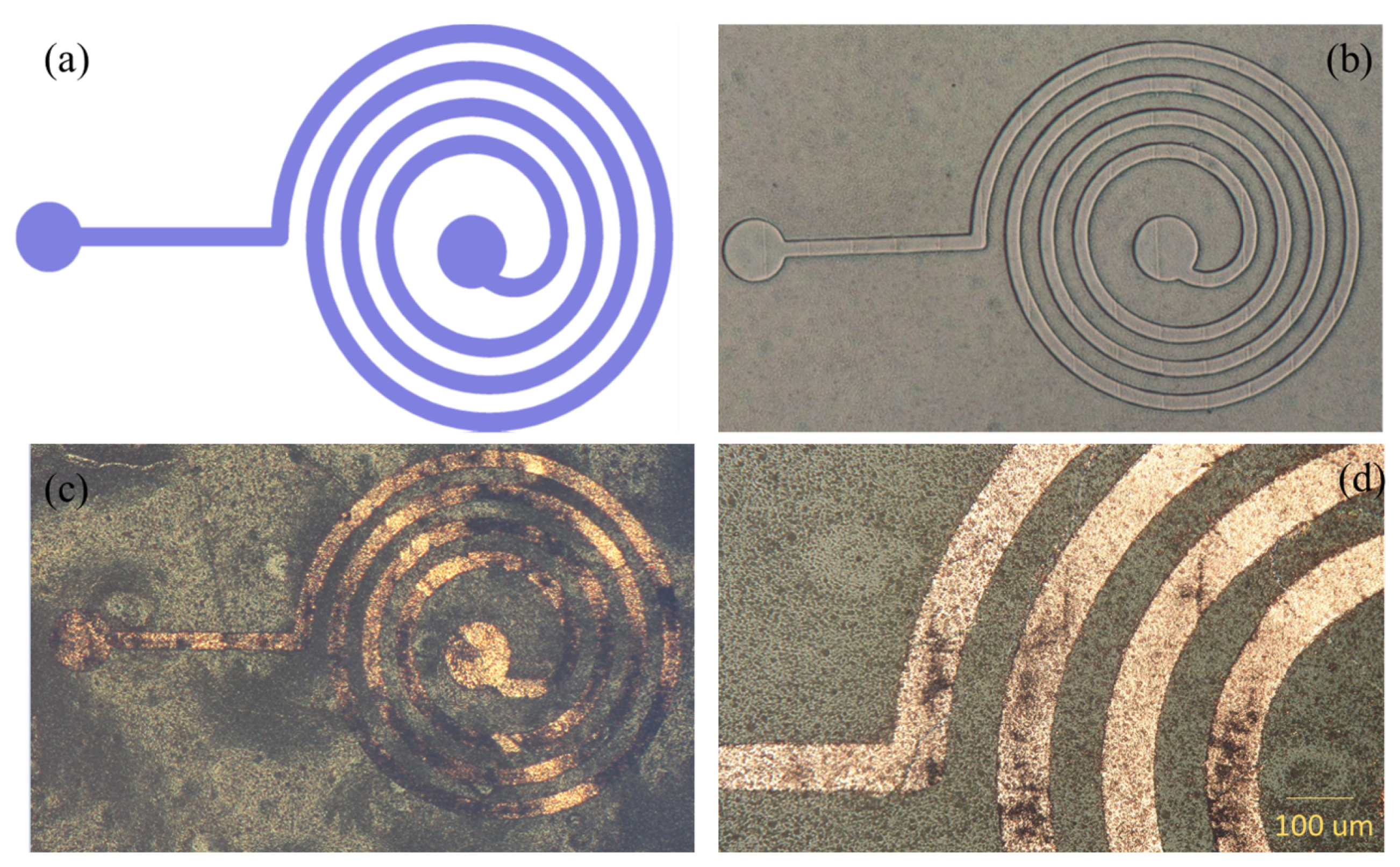
3.4. Fabrication of Planar Inductor: A Use-Case
3.4.1. Objectives
3.4.2. Materials and Methods
3.4.3. Results
4. Summary and Conclusions
Author Contributions
Funding
Institutional Review Board Statement
Informed Consent Statement
Data Availability Statement
Acknowledgments
Conflicts of Interest
Sample Availability
References
- Lee, H.J.; Yu, J. Method of Manufacturing Printed Circuit Board and Multi-Layered PCB. U.S. Patent 6,902,660, 7 June 2005. [Google Scholar]
- Kobayashi, T.; Kawasaki, J.; Mihara, K.; Honma, H. Via-filling using electroplating for build-up PCBs. Electrochim. Acta 2001, 47, 85–89. [Google Scholar] [CrossRef]
- Cheng, Y.L.; Lee, C.Y.; Huang, Y.L. Copper Metal for Semiconductor Interconnects. In Noble and Precious Metals—Properties, Nanoscale Effects and Applications; Intechopen: London, UK, 2018; Chapter 10. [Google Scholar]
- Frater, M.S. Copper/Steel Laminated Sheet for Use in Manufacturing Printed Circuit Boards. U.S. Patent 6,129,990, 10 October 2000. [Google Scholar]
- Betancourt, T.; Brannon-Peppas, L. Micro-and nanofabrication methods in nanotechnological medical and pharmaceutical devices. Int. J. Nanomed. 2006, 1, 483. [Google Scholar] [CrossRef] [PubMed]
- Ra, S.; Lee, C.; Cho, J.; Lee, S.; Lee, J.; Hong, M.; Kwak, J. Micro via and line patterning for PCB using imprint technique. Curr. Appl. Phys. 2008, 8, 675–678. [Google Scholar] [CrossRef]
- Murphy, O.J.; Hitchens, G.D.; Hodko, D.; Clarke, E.T.; Miller, D.L.; Parker, D.L. Method of Using Conductive Polymers to Manufacture Printed Circuit Boards. U.S. Patent 5,545,308, 13 August 1996. [Google Scholar]
- Tamm, W.; Olbrich, W.; Dippon, S.; Weitmann, M.; Lam, S. Method of Manufacturing Printed Circuit Boards. U.S. Patent 5,666,722, 16 September 1997. [Google Scholar]
- Plovie, B.; Yang, Y.; Guillaume, J.; Dunphy, S.; Dhaenens, K.; Van Put, S.; Vandecasteele, B.; Vervust, T.; Bossuyt, F.; Vanfleteren, J. Arbitrarily shaped 2.5 d circuits using stretchable interconnects embedded in thermoplastic polymers. Adv. Eng. Mater. 2017, 19, 1700032. [Google Scholar] [CrossRef]
- Rötting, O.; Röpke, W.; Becker, H.; Gärtner, C. Polymer microfabrication technologies. Microsyst. Technol. 2002, 8, 32–36. [Google Scholar] [CrossRef]
- Becker, H.; Gärtner, C. Polymer microfabrication technologies for microfluidic systems. Anal. Bioanal. Chem. 2008, 390, 89–111. [Google Scholar] [CrossRef] [PubMed]
- Goosey, M.T. Plastics for Electronics, 2nd ed.; Springer: Dordrecht, The Netherlands, 1999. [Google Scholar]
- Varadarajan, M.G.; Lee, K.J.; Bhattacharya, S.K.; Pucha, R.; Tummala, R.R.; Sitaraman, S. Printed circuit board (PCB) miniaturization by embedded passives and sequential build-up (SBU) process methodology. J. Indian Inst. Sci. 2013, 86, 639. [Google Scholar]
- Knudsen, P.; Brainard, R.; Schell, K. A photoimageable dielectric for sequential PWB fabrication. Circuit World 1995, 21, 5–9. [Google Scholar] [CrossRef]
- Fierro, L.; Getty, J.D. Plasma processes for printed circuit board manufacturing. Circuitree-Campbell 2003, 16, 28–33. [Google Scholar]
- Yung, K.; Liem, H.; Choy, H.; Yue, T. Impact of plasma etching on fabrication technology of liquid crystal polymer printed circuit board. J. Mater. Sci. Mater. Electron. 2010, 21, 954–962. [Google Scholar] [CrossRef]
- Shin, J.H.; Park, J.H.; Seo, J.; Im, T.H.; Kim, J.C.; Lee, H.E.; Kim, D.H.; Woo, K.Y.; Jeong, H.Y.; Cho, Y.H.; et al. A Flash-Induced Robust Cu Electrode on Glass Substrates and Its Application for Thin-Film μLEDs. Adv. Mater. 2021, 33, 2007186. [Google Scholar] [CrossRef] [PubMed]
- Weng, Y.; Chen, S.; Zhang, Y.; Sun, L.; Wu, Y.; Yan, Q.; Guo, T.; Zhou, X.; Wu, C. Fabrication and color conversion of patterned InP/ZnS quantum dots photoresist film via a laser-assisted route. Opt. Laser Technol. 2021, 140, 107026. [Google Scholar] [CrossRef]
- Zhao, Y.; Liu, H.; Yu, T.; Hong, M. Fabrication of high hardness microarray diamond tools by femtosecond laser ablation. Opt. Laser Technol. 2021, 140, 107014. [Google Scholar] [CrossRef]
- Zhang, Q.; Huang, D.; Qi, D.; Zhou, W.; Wang, L.; Zhang, Z.; Chen, S.; Dai, S.; Zheng, H. Mask-free patterning of Cu mesh as smart windows by spatially modulated nanosecond laser pulses. Opt. Laser Technol. 2021, 140, 107056. [Google Scholar] [CrossRef]
- Trantidou, T.; Friddin, M.S.; Gan, K.B.; Han, L.; Bolognesi, G.; Brooks, N.J.; Ces, O. Mask-free laser lithography for rapid and low-cost microfluidic device fabrication. Anal. Chem. 2018, 90, 13915–13921. [Google Scholar] [CrossRef] [PubMed]
- Miao, Y.; Wan, L.; Ling, X.; Chen, B.; Pan, L.; Gao, Y. Mask-free preparation of patterned carbonized carboxymethyl cellulose on fabrics for flexible electronics. ACS Appl. Electron. Mater. 2020, 2, 855–862. [Google Scholar] [CrossRef]
- Hollman, R.; Dimov, O.; Malik, S.; Hichri, H.; Arendt, M. Ultra fine RDL structure fabrication using alternative patterning and bottom-up plating processes. In Proceedings of the 2018 IEEE 68th Electronic Components and Technology Conference (ECTC), San Diego, CA, USA, 29 May–1 June 2018; pp. 58–63. [Google Scholar]
- Woehrmann, M.; Wuensch, O.; Lang, K.D.; Gernhard, R.; Hauck, K.; Kroehnert, K.; Zoschke, K.; Juergensen, N.; Toepper, M.; Braun, T.; et al. New Excimer Laser-Based Dual Damacene Process For High I/O Applications with Ultra-Fine Line Routing. Süss Rep. 2016, 2016, 4–10. [Google Scholar]
- Acharya, S.; Chouhan, S.S.; Delsing, J. Scalability of Copper-Interconnects down to 3 μm on Printed Boards by Laser-assisted-subtractive process. In Nordic Conference on Microelectronics Packaging, NORDPAC (Device Packaging, HiTEC, HiTEN, & CICMT); International Microelectronics Assembly and Packaging Society (IMAPs): Copenhagen, Denmark, 2019; Volume 2019, pp. 000017–000020. [Google Scholar]
- Çakır, O. Review of etchants for copper and its alloys in wet etching processes. In Key Engineering Materials; Trans Tech Publications Ltd.: Stafa-Zurich, Switzerland, 2008; Volume 364, pp. 460–465. [Google Scholar] [CrossRef]
- Cakir, O. Copper etching with cupric chloride and regeneration of waste etchant. J. Mater. Process. Technol. 2006, 175, 63–68. [Google Scholar] [CrossRef]
- Dunn, T. Additive Electronics: PCB Scale to IC Scale. Available online: http://www.magazines007.com/pdf/PCB007-Sept2018.pdf (accessed on 24 August 2021).
- Dharmarathna, S.; Clark, T.; Bae, C.; Kil, E.; Bang, A.; Sy, M.; Yeh, R.; Feng, K. Copper Electroplating Processes for Advanced HDI Applications. In Proceedings of the 2019 14th International Microsystems, Packaging, Assembly and Circuits Technology Conference (IMPACT), Taipei, Taiwan, 23–25 October 2019; pp. 84–87. [Google Scholar]
- Mavliev, R.; Gottfried, K.; Rhoades, R. Advanced Packaging Cost Reduction by Selective Copper Metallization. In Proceedings of the 2020 IEEE 70th Electronic Components and Technology Conference (ECTC), Orlando, FL, USA, 3–30 June 2020; pp. 327–332. [Google Scholar]
- Acharya, S.; Chouhan, S.S.; Delsing, J. An Additive Production approach for Microvias and Multilayered polymer substrate patterning of 2.5 μm feature sizes. In Proceedings of the 2020 IEEE 70th Electronic Components and Technology Conference (ECTC), Orlando, FL, USA, 3–30 June 2020; pp. 1304–1308. [Google Scholar]
- Stojanovic, G.; Zivanov, L. Comparison of optimal design of different spiral inductors. In Proceedings of the 2004 24th International Conference on Microelectronics (IEEE Cat. No. 04TH8716), Nis, Serbia, 16–19 May 2004; Volume 2, pp. 613–616. [Google Scholar]
- Multi-cb Printed Circuit Boards/Data Sheet. Available online: https://www.multi-circuitboards.eu (accessed on 24 August 2021).
- Precision Urethane & Machine, Inc. Available online: https://www.precisionurethane.com/urethane-advantage.html (accessed on 24 August 2021).
- Johan Lundqvist, F.V. J-KEM International. Available online: http://jkem.se (accessed on 24 August 2021).
- Acharya, S.; Chouhan, S.S.; Delsing, J. Realization of Embedded Passives using an additive Covalent bonded metallization approach. In Proceedings of the 2019 22nd European Microelectronics and Packaging Conference & Exhibition (EMPC), Pisa, Italy, 16–19 September 2019; pp. 1–6. [Google Scholar]
- Atthoff, B.; Göthe, S. Metalization of Surfaces. U.S. Patent 10,822,702, 16 February 2017. [Google Scholar]
- Chammas, H. Embedded Passive Technology. 2012. Available online: https://docplayer.net/29645317-Embedded-passive-technology.html (accessed on 24 August 2021).
- Gerke, R.D. Embedded passives technology. Resistor 2005, 146, 635. [Google Scholar]
- Stalf, S. Printed inductors in RF consumer applications. IEEE Trans. Consum. Electron. 2001, 47, 426–435. [Google Scholar] [CrossRef]


| Electroless Copper Bath Parameters | |||||
|---|---|---|---|---|---|
| Type | Name | Concentration | Time (in Minutes) | Temperature (°C) | |
| I | Predip | Precup-128 | 55.5 mL in 200 mL of DIW | 1 | 25 |
| II | Activator | Catcup-207 | 55.5 mL in 200 mL of DIW | 6 | 42 |
| III | Reducer | Boric acid + ACS-2075 | 2.4 g in 100 mL of DIW + 1.5 mL of ACS-2075 | 6 | 27 |
| IV | Cu Bath | PEC-660 (A/M/B) | 9.25 mL of PEC-A + 6.75 mL of PEC-M + 9.75 mL of PEC-B in 100 mL of DIW | 4–6 | 25 |
| Feature Size in the Pattern (in m) | Laser Gain (mW) | D-Step (80 m/s) | No. of Repetition |
|---|---|---|---|
| 30 and above | 6.6 | 4.0 | 6.0 |
| 10 | 6.5 | 4.0 | 6.0 |
| 7.5 | 6.4 | 4.0 | 5.0 |
| 5 | 6.5 | 2.0 | 3.0 |
| 2.5 | 6.5 | 2.0 | 3.0 |
Publisher’s Note: MDPI stays neutral with regard to jurisdictional claims in published maps and institutional affiliations. |
© 2021 by the authors. Licensee MDPI, Basel, Switzerland. This article is an open access article distributed under the terms and conditions of the Creative Commons Attribution (CC BY) license (https://creativecommons.org/licenses/by/4.0/).
Share and Cite
Acharya, S.; Chouhan, S.S.; Delsing, J. Fabrication Process for On-Board Geometries Using a Polymer Composite-Based Selective Metallization for Next-Generation Electronics Packaging. Processes 2021, 9, 1634. https://doi.org/10.3390/pr9091634
Acharya S, Chouhan SS, Delsing J. Fabrication Process for On-Board Geometries Using a Polymer Composite-Based Selective Metallization for Next-Generation Electronics Packaging. Processes. 2021; 9(9):1634. https://doi.org/10.3390/pr9091634
Chicago/Turabian StyleAcharya, Sarthak, Shailesh Singh Chouhan, and Jerker Delsing. 2021. "Fabrication Process for On-Board Geometries Using a Polymer Composite-Based Selective Metallization for Next-Generation Electronics Packaging" Processes 9, no. 9: 1634. https://doi.org/10.3390/pr9091634
APA StyleAcharya, S., Chouhan, S. S., & Delsing, J. (2021). Fabrication Process for On-Board Geometries Using a Polymer Composite-Based Selective Metallization for Next-Generation Electronics Packaging. Processes, 9(9), 1634. https://doi.org/10.3390/pr9091634