Article

Detailed Characterization of a Fully Additive Covalent Bonded PCB Manufacturing Process (SBU-CBM Method)

1
Embedded Internet System Lab, Department of Computer Science, Electrical & Space Engineering, Luleå University of Technology, 97187 Luleå, Sweden
2
Department of Information Technology & Electrical Engineering, University of Oulu, 90570 Oulu, Finland
3
Department of Physics & Electrical Engineering, Linnæus University, 39231 Kalmar, Sweden
*
Author to whom correspondence should be addressed.
Processes 2022, 10(4), 636; https://doi.org/10.3390/pr10040636
Submission received: 20 December 2021 / Revised: 14 March 2022 / Accepted: 18 March 2022 / Published: 24 March 2022

Abstract

:
To bridge the technology gap between IC-level and board-level fabrications, a fully additive selective metallization has already been demonstrated in the literature. In this article, the surface characterization of each step involved in the fabrication process is outlined with bulk metallization of the surface. This production technique has used polyurethane as epoxy resin and proprietary grafting chemistry to functionalize the surface with covalent bonds on an FR-4 base substrate. The surface was then metalized using an electroless copper (Cu) bath. This sequential growth of layers on top of each other using an actinic laser beam and palladium (Pd) ions to deposit Cu is analyzed. State-of-the-art material characterization techniques were employed to investigate process mechanism at the interfaces. Density functional theory calculations were performed to validate the experimental evidence of covalent bonding of the layers. This manufacturing approach is capable of adding metallic layers in a selective manner to the printed circuit boards at considerably lower temperatures. A complete analysis of the process using bulk deposition of the materials is illustrated in this work.

1. Introduction

The industrial revolution is in its fourth version and the printing revolution is in its third in the current global market. The use of printing technologies in electronics manufacturing is growing in a wide range of applications. The two big complementary technologies in electronic productions are conventional electronics using Silicon materials and printed electronics (PE) for creating metallic patterns on PCBs [1,2]. Advantages of PE technology are its low-cost fabrication, high volume market segment, high throughput production, lightweight and flexible devices, versatile electronics functionalities, and simple fabrication processes [3,4]. Modern applications of PE technology include data carrier devices, barcodes, radio frequency identitfication (RFID) devices, gas sensors, biosensors, temperature indicators, gas indicators, freshness indicators, flexible packagings, and many more [5,6].
At the industrial level, these PE fabrication technologies are enhanced with novel materials and new processes. Based on the fabrication methodologies, the processes are broadly classified into two types, namely contact techniques and non-contact techniques. In contact PE techniques, the printing plates make direct contact with the substrate, e.g., soft lithography, flexography, gravure printing, and screen printing. On the other hand, in non-contact PE techniques, only deposition materials come in contact with the substrate, like ink-jet printing, aerosol printing, and laser direct printing (LDW) [7,8,9]. Among the three types of substrate materials that are extensively in use are glass fiber, metal, and polymers. The usage of polymeric materials and hybrid (ceramic) substrates in the electronics manufacturing industry has increased in recent years [7,10]. The fabrication process, presented in this paper, comes under non-contact PE technology which uses the LDW technique to make Cu interconnects with polymer-composite-based surface modification [11,12,13].
In recent applications, primarily two additive material deposition techniques are used to pattern metallic traces on flexible substrates, i.e., parallel and sequential methods. Direct-write material deposition technology falls under sequential methods, which have the capabilities to create patterns with minimum feature sizes and resolution [14,15,16,17]. As most of the electronics production methods have started using polymers, the metallization process is thus facing challenges such as higher temperature deposition, uniformity, step coverage, throughput, etc. The various metallization techniques revealed so far are: physical vapor deposition, chemical vapor deposition, electrolytic coating, electroforming, thermal spray, cold spray, electroplating, and electroless plating [18,19,20,21]. In most of these processes, electroless deposition (ELD) has been used for metallization as it gives better uniformity, lesser porosity, and good adhesion to non-conducting surfaces [22]. Some of the recent studies reported semi-additive metallization by electroless Copper (Cu) plating via surface activation, both in integrated circuits (ICs) and printed circuit boards (PCBs) [23,24,25]. Nevertheless, these methods still use metal removal steps in their production approach. Hence, metallization processes for PCBs still need improvizations. The present paper demonstrates an electroless Cu metallization process for PCBs without any metal etching. The methodology shown in this work is a combination of sequential processes (LDW technique for activation of bulk surfaces/specific patterns) followed by a parallel process (for metallization).
Concerning the fabrication gaps related to PCBs, those of ICs, a fully additive approach for PCBs has been demonstrated in previous literature [11,13,26]. The objectives of developing such a manufacturing process are to avoid adding extra steps to the process, achieve feature sizes comparable to the ICs, and replace the solder joints with printed electronic metallic interconnects. So far, a minimum of 2.5 μ m feature sizes has been achieved [11]. The replacement of bulky capacitors and inductors with embedded passives was demonstrated using this fabrication technique [13,26]. However, the steps involved in this production recipe have not been shown yet. Using an interface science approach and connectivity analysis, the process of how the metallization of the substrate is accomplished is investigated and presented in this article.
Sequential Build Up-Covalent Bonded Metallization (SBU-CBM) is the name given to this fully additive fabrication method, and the recipe of the method is shown in Figure 1. In Figure 1, the steps are shown to obtain a bulk Cu on the FR-4. In total, there are seven steps involved and are marked numerically in the process flow. Step 4, in Figure 1, is the deciding step for selective metallization with specific patterns. The electroless plating step (Step 7) shown in the process flow comprises four different baths as indicated in the literature [11]. A detailed mention about the baths is presented in Section 4. This surface activation step can use physical mask or computer-aided design (CAD) file masks to create printed designs on board. Surface activation of CBM chemistry can be performed with LASER (laser lithography)/optical radiation (optical lithography). In the present work, bulk metalized samples were used.
In this paper, further investigation of the process involved in this fully additive method has been conducted. The main highlights of the work are:
  • To demonstrate, in detail, the fabrication steps involved in a fully additive fabrication, i.e., SBU-CBM method.
  • To show the surface modification mechanism and the metallization technique using different characterizations and complementary DFT.
  • To combine the analysis from experimental and simulation results towards concretization of a production technique useful in printed electronics.
In Section 2, the experimental methodology embraced to illustrate the surface mechanism of the SBU-CBM method is displayed. The computational methods employed to the investigation are shown in Section 3. Section 4 outlines the results of different characterization and analyses of the production technique. Section 5 summarizes the work and briefly mentions the future work related to the manufacturing process.

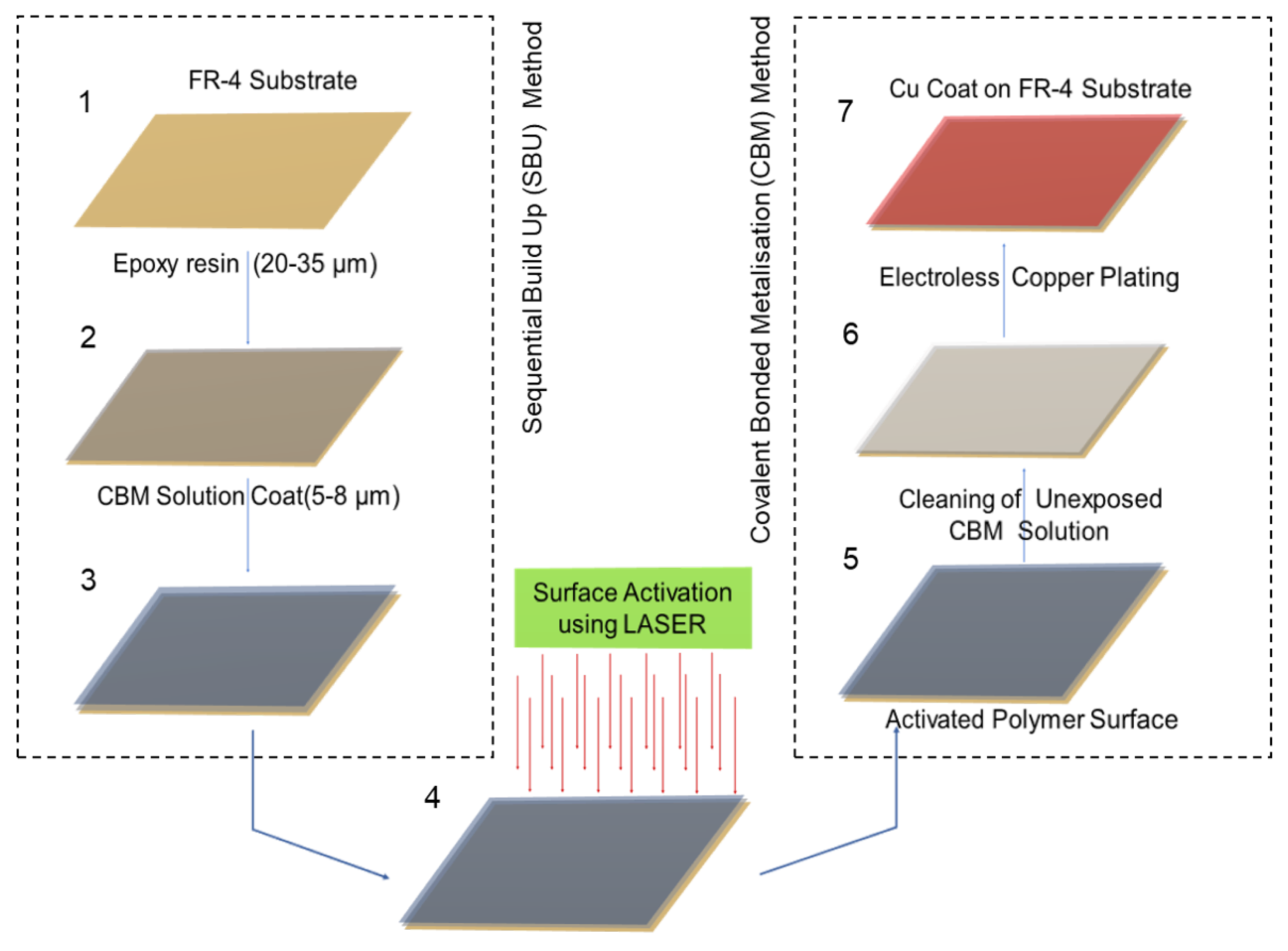
2. Experimental Methods

This section outlines the methodology and materials used to showcase the mechanism involved in the fabrication steps.

2.1. Materials and Sample Preparation
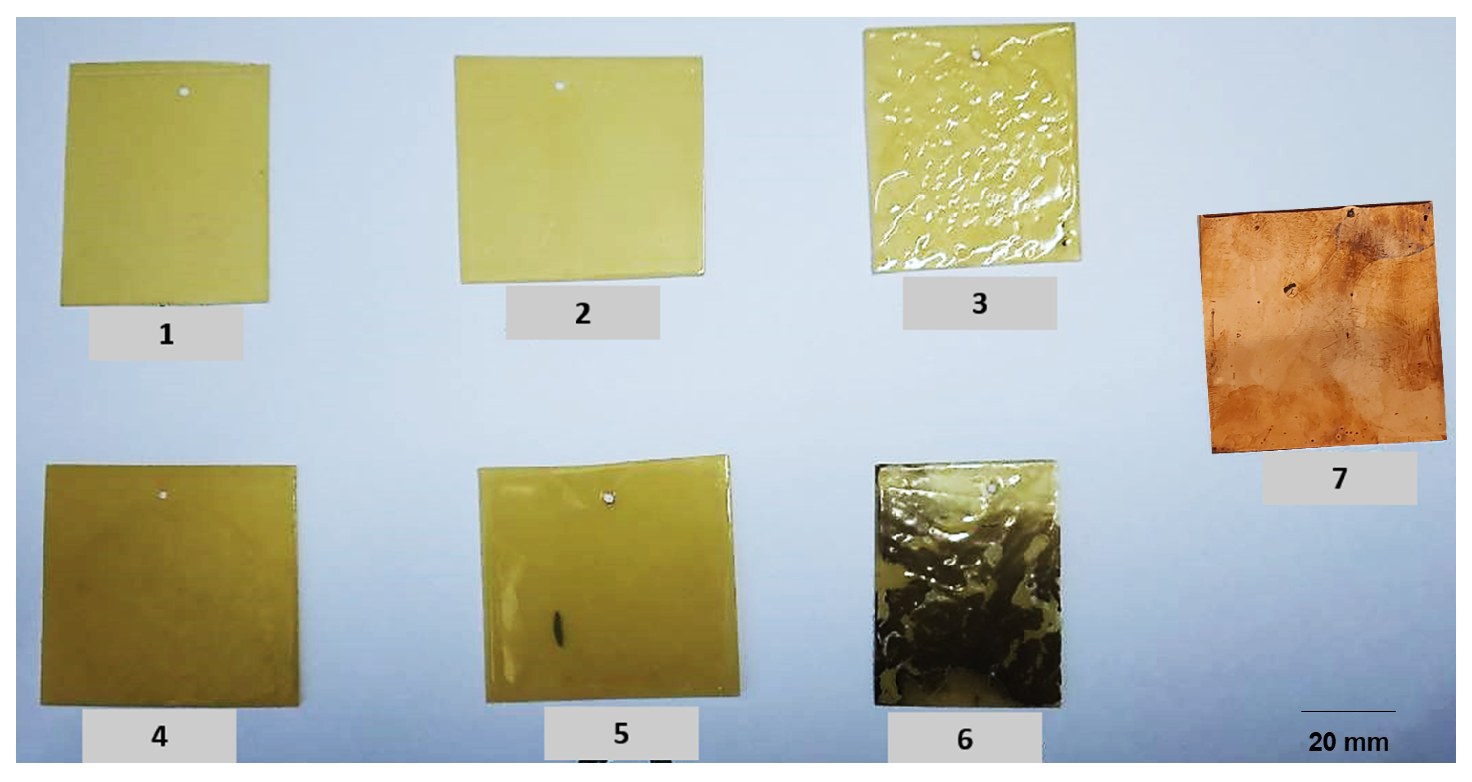
The tests were performed using a 375 nm solid-state GaN laser. The CBM chemistry (HP-14), polyurethane (PU), and electroless kit (PEC-660 series) were used during the investigation. Cuptronics AB, Stockholm supplied the proprietary CBM chemistry (HP-14), Sweden [27]. Electroless Cu bath (PEC-660 series) was purchased from J-KEM International, Stockholm, Sweden [28]. This method has been demonstrated for creating geometries with selective metallization [13]. The focus of this study is to examine the surface modification phenomena during each step of the SBU-CBM process to obtain the final Cu metallization. Therefore, a test specimen with bulk surface has been investigated. Four identical sets of samples, each with seven specimens, were prepared. Figure 2 depicts a group of seven samples. The image quality of the test specimens is compromised due to light reflection from their translucent surfaces. The starting thickness of the samples (Sample 1) is around 0.8–0.9 mm. The Sample 3 shown in Figure 2 is before the cleaning of its surface (with DIW), and such is the reason for its irregular surface. The samples are described in detail below:
Sample 1:
Only FR-4.
Sample 2:
Polyurethane (PU) spin-coated on top of FR-4.
Sample 3:
Polymerized CBM solution (HP-14) seed layer on top of PU and FR-4 (sample with laser activation and without cleaning of the surface).
Sample 4:
After the predip bath immersion (Bath-1).
Sample 5:
After the activator bath immersion (Bath-2).
Sample 6:
After the reducer bath immersion (Bath-3).
Sample 7:
After the Cu bath immersion (Bath-4).

2.2. Chemical Constituents and Methodology

One of the key elements in this production process is the CBM solution, which contains active monomers and spacers in it [29]. In this case, HP-14 is used, which has acrylic acid as an active monomer, ester of acrylic acid, and amide of acrylic acid as spacers. The proportion of spacers in the solution is very minimal compared to the active monomers. Spacers direct and control the optical properties of the active monomers. Nevertheless, only active monomers participate in the surface modification process. An engineering overview of the crucial steps in the surface modification is shown in Figure 3.
In Figure 3a, a seed layer of the CBM solution is spin-coated and exposed under actinic radiation. The double bonds (C=C) in the acrylic acid (CH 2 =CH-COOH) undergo the polymerization reaction. Some of the monomers receive an adequate amount of energy from ultra-violet (UV) radiation to polymerize and some of them remain as is, as shown in Figure 3b. The next important step is to remove the unactivated monomers by properly rinsing and cleaning the sample with de-ionized water (DIW) as shown in Figure 3c. By cleaning the sample, absorption of the metal ions in further steps can be optimized. Then the samples undergo with electroless bath to get metalized. The electroless bath is a package of four different baths [11] and a very first layer of Cu is attached to the activated region during the final bath, as shown in Figure 3d. Then, the bulk Cu layer can be deposited after 3–5 min of long immersion in the final bath, as shown in Figure 3e. In general, the thickness of the Cu varies from 0.3–1.0 μ m. These are some of the major surface modification steps in the SBU-CBM fabrication process. The samples shown in Figure 2 were prepared through these steps for further investigation. Figure 3a–c relates to Sample 3, whereas Figure 3d,e corresponds to Sample 7.

2.3. Characterization

To explore the surface mechanism of this Cu metallization process, a few characterizations were completed such as X-ray diffraction (XRD), scanning electron microscopy (SEM), and energy-dispersive X-ray spectroscopy (EDS). Samples from each step of the SBU-CBM method (as shown in Figure 1) were inspected using a high-resolution SEM (JSM-IT300) by JEOL Inc. Afterward, the samples were investigated through EDS to clarify the mechanism at each interface. The surface of the samples was tested under XRD to check the crystallinity of the deposited Cu. With the help of crystallographic information, a density functional theory (DFT) simulation of the CBM approach was conducted. The results from the DFT are complementing the experimental results. The characterization results and the description of the important surface mechanism in the fabrication are outlined in the section below.

3. Computational Methods

We performed DFT calculations using the projector-augmented wave method [30,31] as implemented in the Vienna Ab-initio Simulation Package (VASP) [32]. For the description of exchange-correlation potential, generalized gradient approximation in the Perdew-Burke-Ernzerhof parametrization was employed [33]. The plane wave cutoff energy was set to a large value of 530 eV. We used a Γ centered Monkhorst-Pack 6 × 6 × 1 k-mesh for the Brillouin zone integration in the structural relaxation, whereas a refined 12 × 12 × 1 k-mesh is used in the self-consistent calculations. In finding the iterative solution of Kohn–Sham equations, a force convergence of 10 2 eV/Å and an energy convergence of 10 6 eV are achieved. Moreover, long-range van der Waals interactions are incorporated using Grimme’s DFT-D3 method [34]. A vacuum layer of 15 Å thickness was inserted in the out-of-plane direction to minimize the effects of three-dimensional periodic boundary conditions. Finally, we used Pyprocar [35] package for pre- and post-processing of the data and plotting of the results.

4. Results and Discussion

In this segment, the results from the characterizations are presented. Analysis of the surface mechanism involved in the fabrication approach has been performed. A clear understanding of surface phenomena in each step and their connection to each other in the SBU-CBM method has been gathered from the SEM-EDS analysis. Using the XRD and evidence from SEM-EDS results, a complementary DFT analysis of the process has also been completed. Finally, the process parameters involved in fabricating the samples were mentioned.

4.1. XRD Analysis

XRD characterization is one of the powerful inspection techniques to understand the properties of an unknown surface. In the present study, XRD analysis has been performed for all the samples; however, the four major steps are illustrated in Figure 4. In Figure 4a, those four steps are shown (from bottom to top), i.e., FR-4 surface (Sample 1), PU on FR-4 (Sample 2), activated CBM solution on PU (Sample 3), and final Cu deposited sample (Sample 7). Figure 4b shows the plot for those four samples, whereas the diffraction peaks on the Cu deposited sample are shown in Figure 4c. Cu is only deposited on Sample 7 as expected following the sequential steps. The diffraction peaks for Cu are: (111) at 43.38, (200) at 50.524, and (220) at 74.24, respectively. The crystal structure was cubic. The objective of this characterization was to observe the properties of Cu and obtain a qualitative analysis of the metallization. Based on the literature [36,37,38], this Cu deposition is perfect for its usage in printed electronics applications. Furthermore, this crystallographic information has been utilized for DFT simulation of the fabrication process.

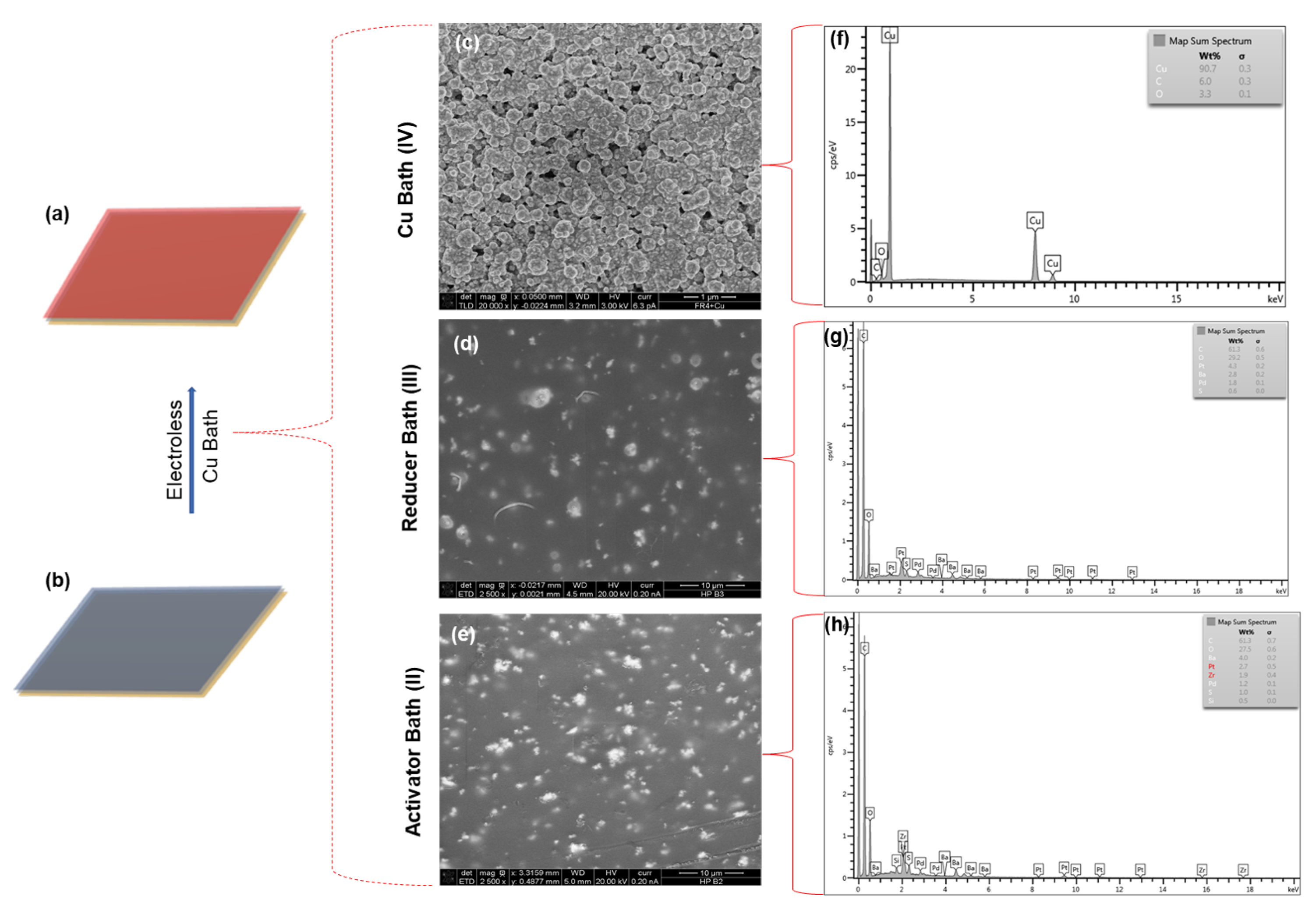
4.2. SEM-EDS Analysis

In the present work, SEM and EDS analysis of the sample’s surface is the imperative characterization to understand the connection of the fabrication steps. Each sample has been inspected and the crucial steps with the analysis are presented below. The analysis has been divided into two parts, i.e., activation of the CBM seed layer for metal ion absorption and electroless Cu plating via catalytic reduction.

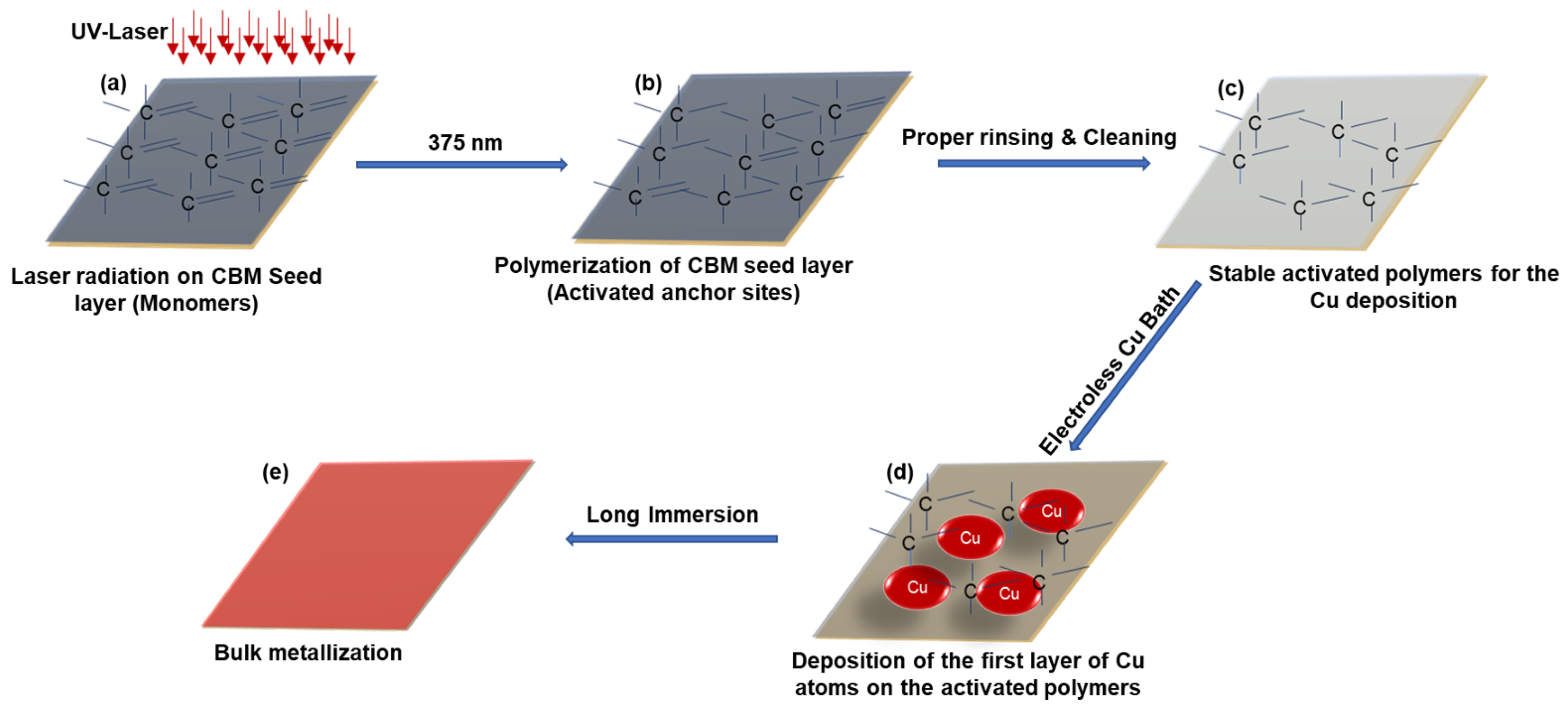
4.2.1. Laser Activation of CBM Seed Layer

The initial step of this production recipe is to build layers on top of each other sequentially [32]. Polyurethane (PU) is the first layer on the FR-4, and a seed layer of the CBM solution is then spin-coated on top of it as the second layer. Due to the evaporating nature of the CBM solution, the seed layer is then exposed to actinic radiation immediately. Steps (a)–(c) in Figure 3 depict the surface mechanism. As illustrated in Figure 3a, double bonds of carbon in acrylic acid become unsaturated when receiving activation energy from UV laser radiation. Meanwhile, some of the double bonds remain and are removed from the surface by thorough washing and rinsing as shown in Figure 3c. The polymerized surface is subsequently immersed in an electroless bath to attach metal ions to it as shown in Figure 3d,e. Surface analysis of these samples is shown in Figure 5. In Figure 5a,b, the fabrication step is shown for which the analysis has been conducted. Figure 5d,f corresponds to Figure 5b, where the SEM image shows showing the surface and spectroscopy data, proving the presence of carbon in abundance (74.5% by wt.). Similarly, Figure 5c,e corresponds to Figure 5a, where the SEM image shows the modified surface and the spectroscopy result shows the stable polymerized carbon (reduced to 61.9 % by wt.) even after proper rinsing and cleaning of the sample. Next step is the deposition of copper as shown in Figure 6.

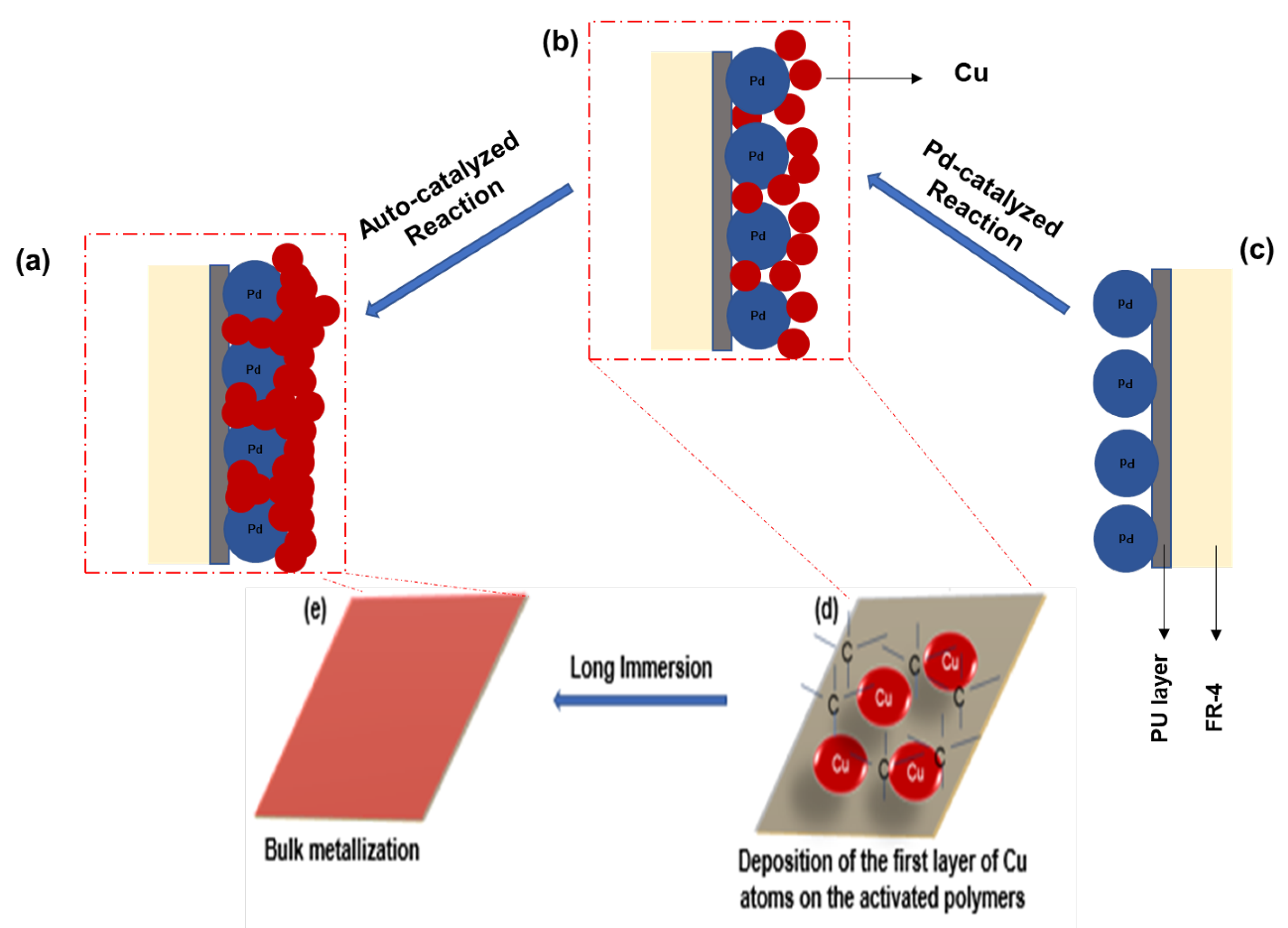
4.2.2. Electroless Copper Plating

After the surface modification by UV radiation, the next step is electroless Cu plating. In this work, we used a proprietary electroless kit by J-KEM International ltd, Stockholm, Sweden. This electroless package has four different baths in it [11,13]. Bath-I, i.e., the predip bath is an alkaline bath used for increasing the receptivity of the substrate. This alkali treatment also enhances the action of the activator bath, i.e., bath-II. However, the influence of bath-II, bath-III, and bath-IV is significant on the metallization and hence thoroughly discussed in the following sections.

Catalytic Behavior of Pd Ion

Bath-II is named the activator bath as it activates the nucleation site for the absorption of Cu ions at a later stage. This bath contains colloidal palladium (Pd) as a catalyst, which is adsorbed onto the sample’s surface. The Pd atoms deposit in embryos and get agglomerated on the surface. In bath-III, which is the reducer bath, the Pd atoms spill over the surface uniformly by breaking the embryos as shown in Figure 7c. The next bath is bath-IV, which contains a Cu-rich aqueous solution. Upon immersing the sample in bath-IV, the absorption property of the Pd atoms creates an initial layer of Cu at the nucleation sites around Pd atom as shown in Figure 7b. This deposition is due to the catalytic action of Pd. Due to the proprietary nature of the materials, the exact composition of the baths is unknown. However, the presence of palladium (Pd) in bath-II and bath-III is indicated from EDS data shown in Figure 6g,h, respectively. As indicated, the weight% of Pd has increased and spread more evenly on the surface of Sample 6 than Sample 5. Figure 6d,e illustrates the surface of Sample 6 and Sample 5, respectively. A similar chemical modification is also reported in previous literature [39,40,41].

Auto-Catalytic Copper Deposition
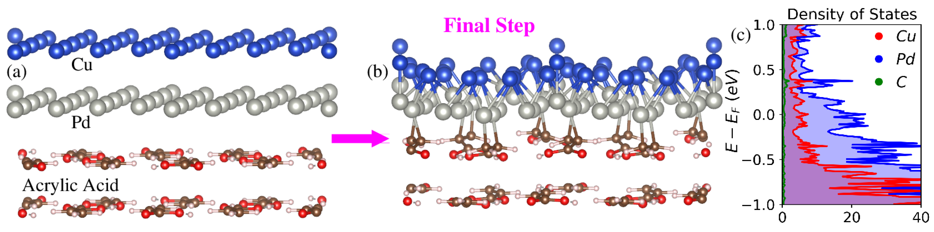
The last step of the SBU-CBM method is Cu bath, i.e., bath-IV. A short immersion into bath-IV forms a layer of nascent Cu as indicated in Figure 7b. Further immersion of the sample in bath-IV (over a duration of 3–5 min) will result in bulk metallization. Each ‘nascent’ Cu atom then acts as a catalyst in itself, and the reaction continues as shown in Figure 7a; hence, it is called ‘auto-catalytic deposition’. Thus, metallization of the surface has a great influence from bath-II and bath-III, as the Pd adsorption is very crucial. In this paper, the catalytic reaction has been observed with Sample 7. The SEM image of Sample 7 is shown in Figure 6c. A uniform layer of Cu has been deposited with proper parameter optimization and controlled fabrication steps. The EDS result related to the Sample 7 is shown in Figure 6f (90% Cu on the surface).

4.3. DFT Analysis

In order to explain underlying mechanism, we performed first-principles calculations based on density functional theory (DFT) for which technical details are given in the computational methods section. Figure 8a shows a schematic view of the molecular structure of acrylic acid (an active monomer in HP-14 samples) having Pd and Cu atomic layers deposited on top to mimic the experimental setup. Owing to the presence of dangling bonds, Pd atoms tend to form covalent bonds with unsaturated C atoms as well as Cu atoms implanted on its surface as displayed in Figure 8b. Moreover, refer to Figure 8c in which we calculate element-projected density of states (DOS) to confirm the characteristic nature of inter-atomic interactions. The presence of orbital hybridization between Cu and Pd d-orbitals close to the Fermi level support these observations.

4.4. Process Parameters

The parameters related to the SBU-CBM method, especially for making geometries and complex structures, vary according to the size of the structures and were already demonstrated in earlier literature [11,27,32]. In this work, the samples were prepared with bulk metallization and hence optimization of the electroless baths was much simpler. HP-14 was used as the CBM chemistry and hence previously optimized parameters were used, i.e., laser gain of 6.5 mW, no. of repetitions was three (11 mins), and scan rate was 160 μ m/s (D-step: 2), already demonstrated in earlier literature [32]. A brief overview of the parameters related to the electroless bath (adjusted for HP-14) is presented in Table 1.

5. Summary and Conclusions

The SBU-CBM fabrication approach has already been proposed in the literature without a detailed study of its fabrication steps. In this work, a detailed mechanism of Cu metallization using a fully additive fabrication approach has been demonstrated. Both the experimental and simulation results related to the metallization process were shown. The SEM-EDS results were well complemented by the DFT simulation results. In summary, the fabrication steps include the first layer of polyurethane and a seed layer of CBM chemistry (HP-14) on top of it. With adequate actinic radiation, the seed layer gets polymerized to adhere metallic ions on it. Bulk metalized samples were investigated in this work. However, the main highlight of the SBU-CBM process is selective polymerization and selective metallization. This fabrication process has the potential of patterning any desired geometry and generating fine Cu interconnects at the board level without the involvement of any etching steps. Future work will be the electrical and reliability testing of the Cu with specific patterns to test the potential of the process for mass production. Furthermore, the observed surface mechanism will be utilized to make multi-layered PCBs and connect physical components without using the soldering process.

Author Contributions

Conceptualization was undertaken by S.A.; S.A. and S.S. designed the experiments; S.A. performed the experiments; S.S. performed the DFT simulation; S.A., S.S.C. and J.D. analyzed the data; S.A. and S.S. wrote the paper; J.D. and S.S.C. reviewed and edited the paper; J.D. supervised the process. All authors have read and agreed to the published version of the manuscript.

Funding

This research was funded by the Interreg Nord, European Regional Development Fund (ERDF) at https://www.interregnord.com/ (accessed on 15 March 2022).

Institutional Review Board Statement

Not applicable.

Informed Consent Statement

Not applicable.

Data Availability Statement

Not applicable.

Acknowledgments

The authors would like to recognize the European project: Productive 4.0 and InterregNord-COMPACT for the budgetary back. The whole work was carried out in the Clean Room, EISLAB, within the department of Computer Science, Electrical and Space Designing, LUT. Moreover, the authors are grateful to Cuptronics AB, Stockholm for supplying the proprietary CBM chemistry and the electroless copper bath. The authors are grateful to Liang Yu for the utilization of SEM-EDS and XRD machines. The computations were enabled by resources provided by the Swedish National Infrastructure for Computing (SNIC) at HPC2N and NSC, partially funded by the Swedish Research Council through Grant Agreement No. 2018-05973. Shahid Sattar thanks Carl Tryggers Stiftelsen (CTS 20:71) for financial support. Lastly, the authors are grateful to Roghayeh Imani for her help amid the paper’s composition.

Conflicts of Interest

The authors declare no conflict of interest.

References

  1. Kantola, V.; Kulovesi, J.; Lahti, L.; Lin, R.; Zavodchikova, M.; Coatanéa, E. 1.3 Printed electronics, now and future. Bit Bang 2009, 63, 204. [Google Scholar]
  2. Suganuma, K. Introduction to Printed Electronics; Springer: Berlin, Germany, 2014; Volume 74. [Google Scholar]
  3. Lee, S.J.; Rahman, A.M. Intelligent Packaging for Food Products; Elsevier: Amsterdam, The Netherlands, 2014; pp. 171–209. [Google Scholar]
  4. Khan, Y.; Thielens, A.; Muin, S.; Ting, J.; Baumbauer, C.; Arias, A.C. A new frontier of printed electronics: Flexible hybrid electronics. Adv. Mater. 2020, 32, 1905279. [Google Scholar]
  5. Cantatore, E. Applications of Organic and Printed Electronics. A Technology-Enabled Revolution; Springer: New York, NY, USA, 2013; p. 180. [Google Scholar]
  6. Izdebska, J. Applications of printed materials. In Printing on Polymers: Fundamentals and Applications; Elsevier: Amsterdam, The Netherlands, 2016; pp. 371–388. [Google Scholar]
  7. Cruz, S.M.F.; Rocha, L.A.; Viana, J.C. Printing technologies on flexible substrates for printed electronics. In Flexible Electronics; IntechOpen: London, UK, 2018; Available online: https://www.intechopen.com/books/6765 (accessed on 15 March 2022).
  8. Cui, Z. Printed Electronics: Materials, Technologies and Applications; John Wiley & Sons: Hoboken, NJ, USA, 2016. [Google Scholar]
  9. Wiklund, J.; Karakoç, A.; Palko, T.; Yiğitler, H.; Ruttik, K.; Jäntti, R.; Paltakari, J. A review on printed electronics: Fabrication methods, inks, substrates, applications and environmental impacts. J. Manuf. Mater. Process. 2021, 5, 89. [Google Scholar]
  10. Yang, C.Y.; Stoeckel, M.A.; Ruoko, T.P.; Wu, H.Y.; Liu, X.; Kolhe, N.B.; Wu, Z.; Puttisong, Y.; Musumeci, C.; Massetti, M.; et al. A high-conductivity n-type polymeric ink for printed electronics. Nat. Commun. 2021, 12, 1–8. [Google Scholar]
  11. Acharya, S.; Chouhan, S.S.; Delsing, J. An Additive Production approach for Microvias and Multilayered polymer substrate patterning of 2.5 μm feature sizes. In Proceedings of the 2020 IEEE 70th Electronic Components and Technology Conference (ECTC), Orlando, FL, USA, 3–30 June 2020; pp. 1304–1308. [Google Scholar]
  12. Acharya, S.; Chouhan, S.S.; Delsing, J. Scalability of Copper-Interconnects down to 3 μ m on Printed Boards by Laser-assisted-subtractive process. In Proceedings of the Additional Conferences (Device Packaging, HiTEC, HiTEN, & CICMT), International Microelectronics Assembly and Packaging Society, Copenhagen, Denmark, 10–13 June 2019; Volume 2019, pp. 17–20. [Google Scholar]
  13. Acharya, S.; Chouhan, S.S.; Delsing, J. Fabrication Process for On-Board Geometries Using a Polymer Composite-Based Selective Metallization for Next-Generation Electronics Packaging. Processes 2021, 9, 1634. [Google Scholar]
  14. Swenson, O.; Marinov, V. Laser processing of direct-write Nano-sized materials. In Advances in Laser Materials Processing; Elsevier: Amsterdam, The Netherlands, 2010; pp. 671–694. [Google Scholar]
  15. Ahn, J.; Sim, H.H.; Kim, J.H.; Wajahat, M.; Kim, J.H.; Bae, J.; Kim, S.; Pyo, J.; Jeon, C.J.; Kim, B.S.; et al. Air-Pressure-Assisted Pen-Nib Printing for 3D Printed Electronics. Adv. Mater. Technol. 2021, 2101172. [Google Scholar] [CrossRef]
  16. Watanabe, A.; Qin, G.; Cai, J. Laser Direct Writing on Copper Nanoparticle Film by LightScribe Technique. J. Photopolym. Sci. Technol. 2015, 28, 99–102. [Google Scholar]
  17. Lewis, J.A.; Ahn, B.Y. Three-dimensional printed electronics. Nature 2015, 518, 42–43. [Google Scholar]
  18. Parmar, H.; Tucci, F.; Carlone, P.; Sudarshan, T. Metallisation of polymers and polymer matrix composites by cold spray: State of the art and research perspectives. Int. Mater. Rev. 2021, 1–25. [Google Scholar] [CrossRef]
  19. Le Lesle, J.; Quemener, V.; Morrand, J.; Perrin, R.; Mrad, R.; Mollov, S. Design, Manufacturing and Evaluation of a Highly Integrated Low-Voltage High-Current Inverter. In Proceedings of the CIPS 2020: 11th International Conference on Integrated Power Electronics Systems, Berlin, Germany, 24–26 March 2020; pp. 1–5. [Google Scholar]
  20. Toh, H.W. Copper Metallisation for High-Density Interconnects and Planar Inductors. Ph.D. Thesis, Queen’s University of Belfast, Northern Ireland, UK, 2002. [Google Scholar]
  21. Wang, J. Electrodeposition and Characterisation of Nickel-Niobium-Based Diffusion Barrier Metallisations for High Temperature Electronics Interconnections. Ph.D. Thesis, Loughborough University, Loughborough, UK, 2016. [Google Scholar]
  22. Kerr, C.; Barker, D.; Walsh, F. Electroless deposition of metals. Trans. IMF 2001, 79, 41–46. [Google Scholar]
  23. Mavliev, R.; Gottfried, K.; Rhoades, R. Advanced Packaging Cost Reduction by Selective Copper Metallization. In Proceedings of the 2020 IEEE 70th Electronic Components and Technology Conference (ECTC), Orlando, FL, USA, 3–30 June 2020; pp. 327–332. [Google Scholar]
  24. Lennon, A.; Colwell, J.; Rodbell, K.P. Challenges facing copper-plated metallisation for silicon photovoltaics: Insights from integrated circuit technology development. Prog. Photovoltaics Res. Appl. 2019, 27, 67–97. [Google Scholar]
  25. Kordás, K.; Nánai, L.; Bali, K.; Stépán, K.; Vajtai, R.; George, T.F.; Leppävuori, S. Palladium thin film deposition from liquid precursors on polymers by projected excimer beams. Appl. Surf. Sci. 2000, 168, 66–70. [Google Scholar]
  26. Acharya, S.; Chouhan, S.S.; Delsing, J. Realization of Embedded Passives using an additive Covalent bonded metallization approach. In Proceedings of the 2019 22nd European Microelectronics and Packaging Conference & Exhibition (EMPC), Pisa, Italy, 16–19 September 2019; pp. 1–6. [Google Scholar]
  27. Atthoff, B.; Göthe, S. Cuptronics Technology; Cuptronic Technology: Stockholm, Sweden; Available online: http://cuptronic.com (accessed on 15 March 2022).
  28. Johan Lundqvist, F.V. J-KEM International. Available online: http://jkem.se (accessed on 15 March 2022).
  29. Atthoff, B.; Göthe, S. Metalization of Surfaces. U.S. Patent 10,822,702, 16 February 2017. [Google Scholar]
  30. Blöchl, P.E. Projector Augmented-Wave Method. Phys. Rev. B 1994, 50, 17953–17979. [Google Scholar] [CrossRef] [Green Version]
  31. Kresse, G.; Furthmüller, J. Efficient Iterative Schemes for Ab Initio Total-Energy Calculations Using a Plane-Wave Basis Set. Phys. Rev. B 1996, 54, 11169–11186. [Google Scholar] [CrossRef]
  32. Kresse, G.; Joubert, D. From Ultrasoft Pseudopotentials to the Projector Augmented-Wave Method. Phys. Rev. B 1999, 59, 1758–1775. [Google Scholar] [CrossRef]
  33. Perdew, J.P.; Burke, K.; Ernzerhof, M. Generalized Gradient Approximation Made Simple. Phys. Rev. Lett. 1996, 77, 3865. [Google Scholar] [CrossRef] [Green Version]
  34. Grimme, S.; Antony, J.; Ehrlich, S.; Krieg, H. A Consistent and Accurate Ab Initio Parametrization of Density Functional Dispersion Correction (DFT-D) For the 94 Elements H-Pu. J. Chem. Phys. 2010, 132, 154104. [Google Scholar] [CrossRef] [Green Version]
  35. Herath, U.; Tavadze, P.; He, X.; Bousquet, E.; Singh, S.; Muñoz, F.; Romero, A.H. PyProcar: A Python Library for Electronic Structure Pre/Post-Processing. Comput. Phys. Commun. 2020, 251, 107080. [Google Scholar] [CrossRef] [Green Version]
  36. Theivasanthi, T.; Alagar, M. X-ray diffraction studies of copper nanopowder. arXiv 2010, arXiv:1003.6068. [Google Scholar]
  37. Hsu, H.H.; Lin, K.H.; Lin, S.J.; Yeh, J.W. Electroless copper deposition for ultralarge-scale integration. J. Electrochem. Soc. 2001, 148, C47. [Google Scholar]
  38. Tracy, D.; Knorr, D.; Rodbell, K. Texture in multilayer metallization structures. J. Appl. Phys. 1994, 76, 2671–2680. [Google Scholar]
  39. Mittal, K.L. Metallized Plastics 5&6: Fundamental and Applied Aspects; VSP: Rancho Cordova, CA, USA, 1998. [Google Scholar]
  40. Ma, Z.; Tan, K.; Kang, E. Electroless plating of palladium and copper on polyaniline films. Synth. Met. 2000, 114, 17–25. [Google Scholar]
  41. Park, N.; Kim, I.W.; Kim, J. Copper metallization of poly (ethylene terephthalate) fabrics via intermediate polyaniline layers. Fibers Polym. 2009, 10, 310–314. [Google Scholar]
Figure 1. The process flow diagram of the SBU-CBM method for bulk Cu metalization.
Processes 10 00636 g001
Figure 2. An overview of the test samples used for the investigation of the surface mechanism.
Processes 10 00636 g002
Figure 3. Surface engineering of the SBU-CBM method. (a) Showing the carbon double bonds in acrylic acid (the primary constituent of the CBM solution seed layer). (b) Partial activation of the double bonds by the actinic radiation and polymerization on polyurethane surface. (c) Stable activated polymers on the sample’s surface after proper cleaning and rinsing. (d) First layer of Cu deposited on the activated polymers. (e) Formation of a uniform layer of Cu at the final step of the SBU-CBM process.
Processes 10 00636 g003
Figure 4. XRD analysis of the SBU-CBM fabrication method. (a) Four important steps in the production approach for which XRD analysis has been carried out. (b) XRD plot for the surface of FR-4, polyurethane, activated CBM solution by UV radiation, and Cu deposited samples, respectively. (c) Separate XRD plot of the Cu deposited sample with the main diffraction peaks.
Processes 10 00636 g004
Figure 5. (a) Step showing the surface after laser activation of CBM solution seed layer. (b) Step showing the PU on top of FR-4. (c) SEM image of the Sample 3. (d) SEM image of the Sample 2. (e) EDS result of Sample 3. (f) EDS result of Sample 2.
Processes 10 00636 g005
Figure 6. (a) Step showing the final step of the SBU-CBM fabrication method with bulk metalized Cu surface. (b) Step showing the surface after laser activation of the CBM solution seed layer. (c) SEM image of Sample 7. (d) SEM image of Sample 6. (e) SEM image of Sample 5. (f) EDS data related to Sample 7. (g) EDS data related to Sample 6. (h) EDS data related to Sample 5.
Processes 10 00636 g006
Figure 7. Mechanism involved in of the (d,e) of Figure 3. (a) Bulk metallization through auto-catalytic deposition (achieved by long immersion in bath-IV, i.e., Sample 7). (b) Deposition of the first Cu layer through Pd-catalytic reduction. (c) Deposition of Pd atom on the surface (Sample 6).
Processes 10 00636 g007
Figure 8. (a) Side view of the acrylic acid having Pd and Cu atomic layers implanted on top. (b) Simulated model after structural relaxation depicting characteristic inter-atomic bonding. (c) Element-projected density of states for the relaxed structure.
Processes 10 00636 g008
Table 1. Process parameters of electroless Cu bath for bulk metallization.
Electroless Copper Bath Parameters
TypeNameConcentartionTime
(min)
Temperature
( C)
IPredipPrecup-12850 mL in 200 mL of DIW125
IIActivatorCatcup-20750 mL in 200 mL of DIW542
IIIReducerBoric acid +
ACS-2075
2.2 gm in 100 mL of DIW +
1.1 mL of ACS-2075
525
IVCu BathPEC-660
(A/M/B)
9.50 mL of PEC-A +
6.75 mL of PEC-M +
9.50 mL of PEC-B in
100 mL of DIW
3–525
Publisher’s Note: MDPI stays neutral with regard to jurisdictional claims in published maps and institutional affiliations.

