Article

Analysis of a PWM Converter with Less Current Ripple, Wide Voltage Operation and Zero-Voltage Switching

Department of Electrical Engineering, National Yunlin University of Science and Technology, Yunlin 640, Taiwan
*
Author to whom correspondence should be addressed.
Processes 2021, 9(4), 580; https://doi.org/10.3390/pr9040580
Submission received: 19 February 2021 / Revised: 18 March 2021 / Accepted: 23 March 2021 / Published: 26 March 2021
(This article belongs to the Special Issue Application of Power Electronics Technologies in Power System)

Abstract

:
This paper studies and implements a power converter to have less current ripple output and wide voltage input operation. A three-leg converter with different primary turns is presented on its high-voltage side to extend the input voltage range. The current doubler rectification circuit is adopted on the output side to have low current ripple capability. From the switching states of the three-leg converter, the presented circuit has two equivalent sub-circuits under different input voltage ranges (Vin = 120–270 V or 270–600 V). The general phase-shift pulse-width modulation is employed to control the presented converter so that power devices can be turned on at zero voltage in order to reduce switching loss. Compared to two-stage circuit topologies with a wide voltage input operation, the presented converter has the benefits of simple circuit structure, easy control algorithm using a general integrated circuit or digital controller, and less components. The performance of the presented circuit is confirmed and validated by an 800 W laboratory prototype.

1. Introduction

For the past decade, clean energy sources have brought attention to the depletion of fossil fuel demand due to the rising demand for electric power. Fuel cell stacks, wind energy, and photovoltaic (PV) are the most attractive renewable energy sources [1,2,3,4,5,6]. However, the output voltage of dc wind power and PV panels is unstable and widely varies. High-frequency dc-link converters can convert an unstable dc voltage to a constant dc voltage by using duty cycle control [7,8,9] or pulse frequency modulation (PFM) [10,11,12]. In duty cycle control, the turn-on time of the power switch is related to input voltage under the constantly switching frequency. Therefore, the load terminal is regulated at the command voltage. In the PFM approach, the switching frequency is variable and related to input voltage. Thus, the input impedance of the resonant tank is variable to change voltage gain and regulate load voltage. For dc wind energy and PV power, the solar intensity and wind speed have a wide deviation. Therefore, the output voltage of PV panels and wind generators is variable in a wide voltage range. In conventional isolated dc converters, the maximum and minimum effective duty cycles are related to input voltage, deff,max/deff,min = Vin,max/Vin,min. In phase-shift pulse-width modulation (PWM) converters, the maximum (or minimum) effective duty cycle or duty ratio is normally less (or greater) than 0.45 (or 0.15). Then, the available input voltage variation range Vin,max/Vin,min is less than 3. However, the output voltage variation of some dc wind power and PV panels may be greater than 4. To overcome this problem, dc converters with a cascaded structure [13,14,15] have been studied which have a wide input voltage variation. The problem with the cascaded structure converters is low efficiency. The dc converters with duty cycle control were studied in [16,17,18] to achieve wide voltage operation and low switching loss. However, the control algorithm is too complicated for using a general-purpose integrated circuit. Full-bridge converters with wide input voltage range that have PWM or PFM schemes have been presented in [19,20]. The input voltage variation range in [20] with two transformers and one ac switch structure could achieve Vin,max/Vin,min = 4. Four equivalent circuits could be operated in [14] to realize wide voltage operation. However, the control scheme is more complicated when using a general-purpose integrated circuit. In [21], a hybrid dc–dc converter is presented to have wide voltage operation between Vin = 120 V and 600 V. However, this converter has more ripple current on the output inductor and more passive components on the secondary side. In [22], a wide voltage resonant converter was discussed and implemented to be operated between Vin = 10 V and 160 V for low-power applications. However, the circuit topology was still a cascaded dc–dc converter.
In the present work, a three-leg structure phase-shift PWM converter is studied and implemented to have a wide voltage input operation and a wide load range of zero-voltage turn-on operation. Two sub-circuits with different voltage gains can be operated in the presented converter according to input voltage ranges. Hence, the presented converter can accomplish wide input voltage operation. The phase-shift PWM approach is used to control the gating signals of power devices. Then, the zero-voltage switching (ZVS) operation for the three-leg converter can be easily achieved. The current doubler rectification circuit is operated on the load terminal. Therefore, the current ripple on the output terminal is decreased. A Schmitt voltage comparator is used in the control circuit to select the proper sub-circuit, having a high voltage gain under a low voltage input range or a low voltage gain under ahigh voltage input range. The reference voltage of the voltage comparator is equal to 270 V. The presented circuit is designed to be operated under Vin = 120~600 V. Compared to the conventional cascaded structure converter in [13,14,15,16,17,18], the studied converter has an easy control algorithm and a simple circuit structure. Compared to conventional converters with a wide voltage operation [19,20,21,22], the proposed converter has fewer active switches and a wider voltage deviation region. The effectiveness and benefits of the presented circuit are verified by theoretical analysis and experimental verifications with an 800 W prototype.

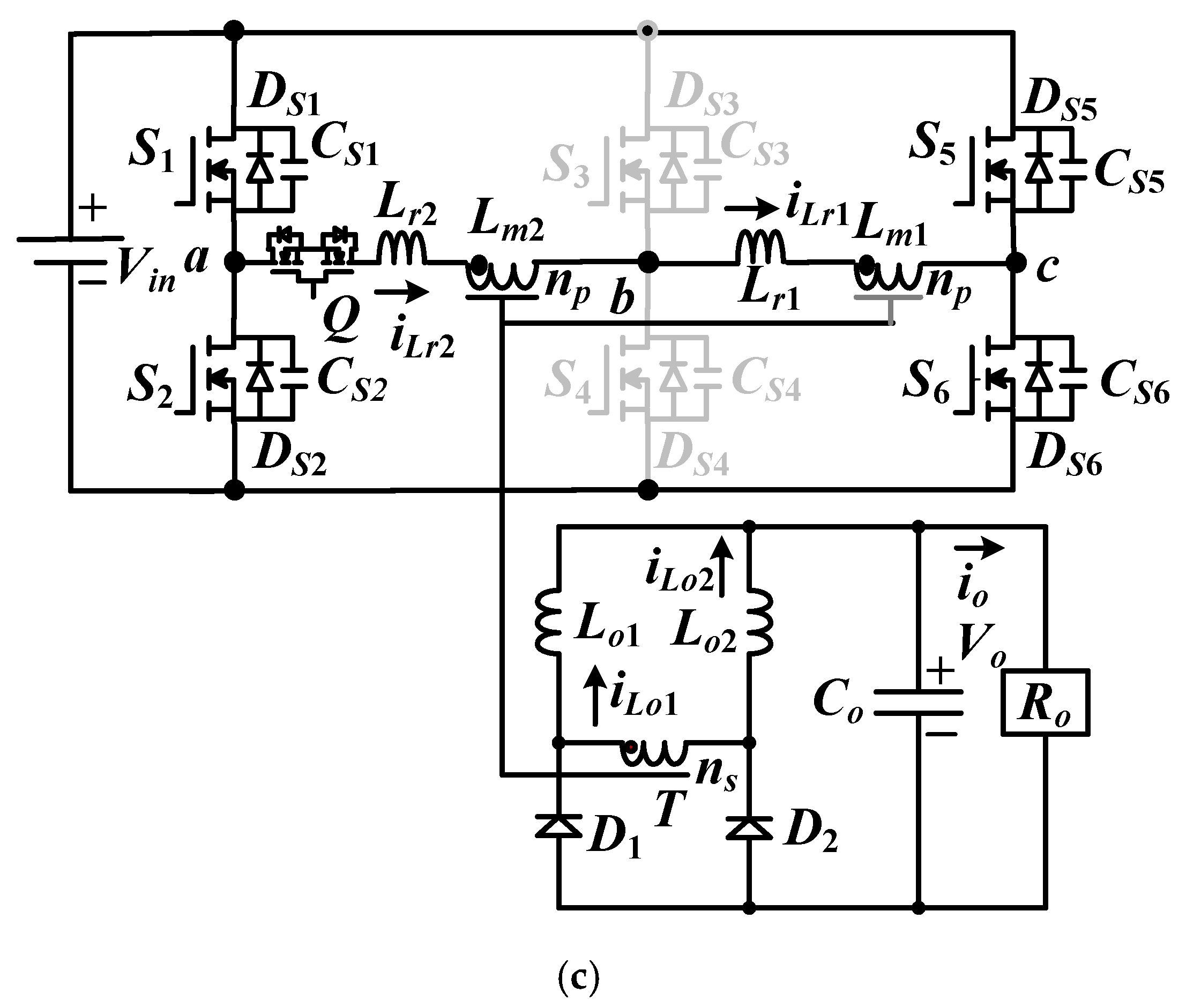
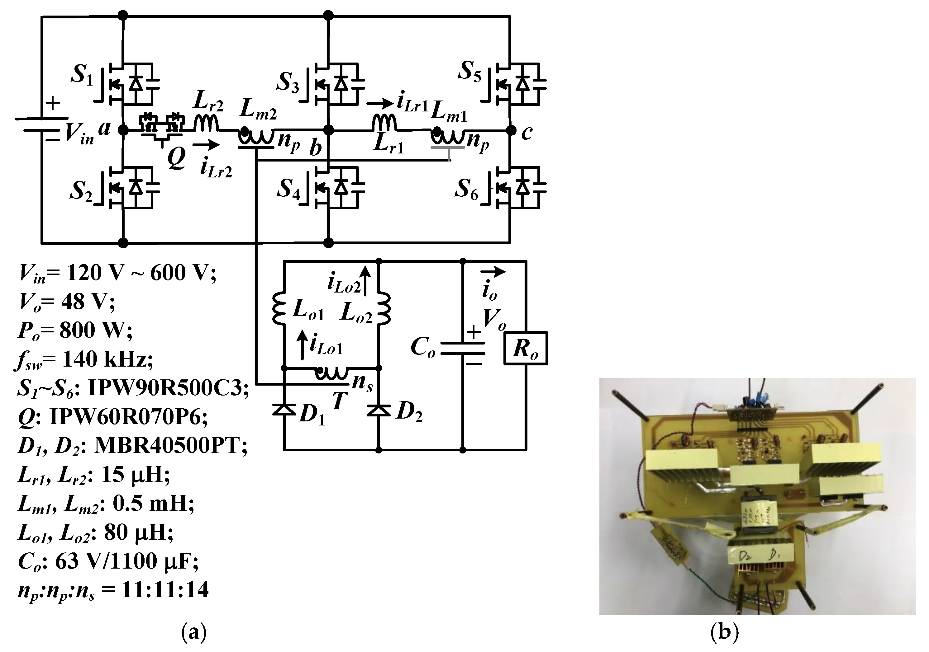
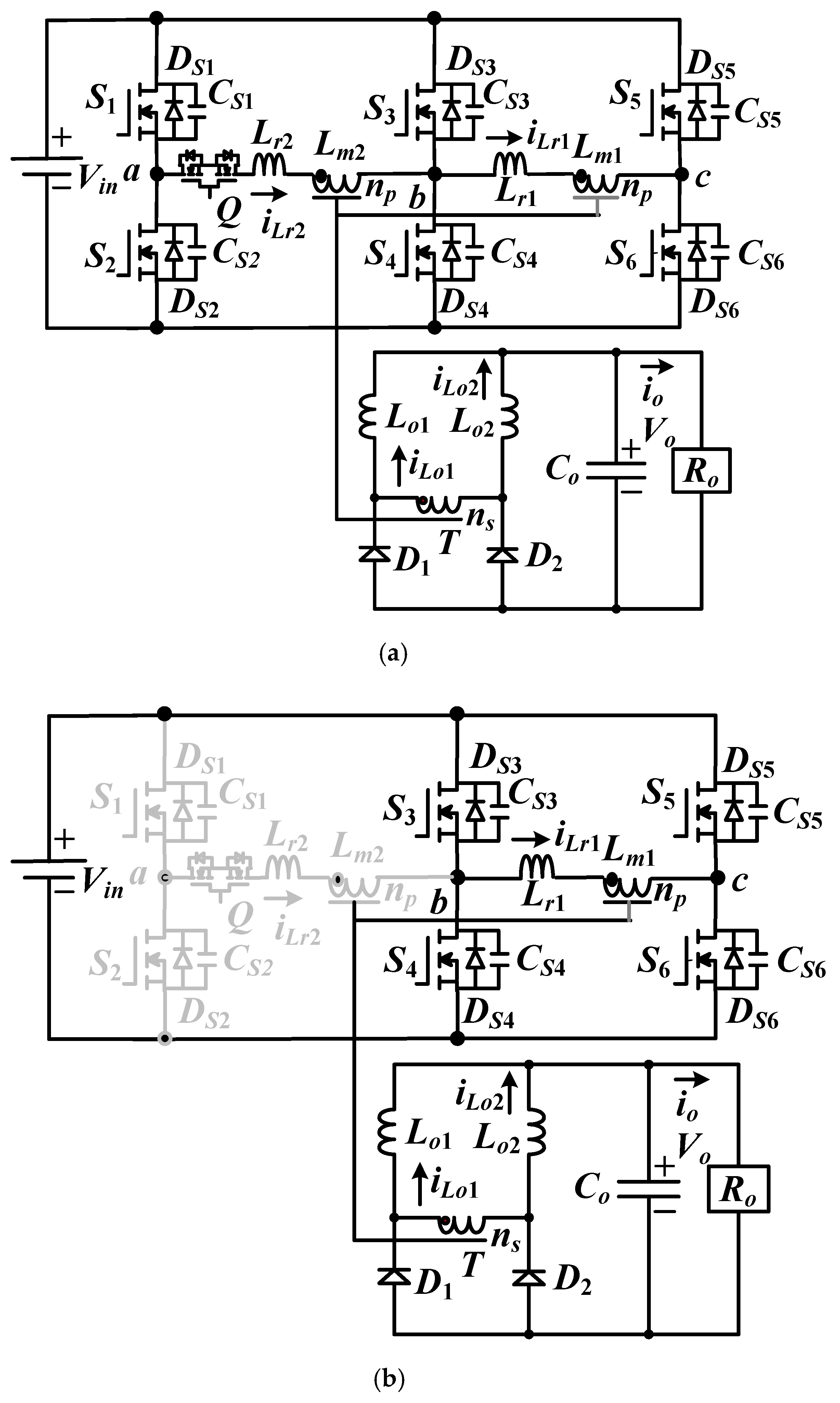
2. Proposed Converter

Figure 1a gives the circuit schematic of the presented converter. It can be observed that the three-leg circuit structure is operated on the primary side and a current doubler rectification structure is adopted on the secondary side. An isolation transformer with two sets of primary-turn np and one set of secondary-turn ns is selected in the converter. The ac switch Q is realized by two power MOSFETs (Metal-Oxide-Semiconductor Field-Effect Transistors) with a back-to-back connection. According to low voltage or high voltage input conditions, Q is controlled to be OFF or ON. Therefore, two equivalent sub-circuits are worked in the presented converter. For a low voltage input region (e.g., Vin,L = Vin,min~2.3Vin,min), Q, S1, and S2 are OFF, and the two-leg PWM converter shown in Figure 1b with active switches S3S6 is operated to regulate the load voltage. The duty cycle control is selected to generate the necessary gate signals of active switches S3S6. Thus, the ZVS operation of S3S6 is achieved. The output voltage can be estimated as V o = n s V i n , L d e f f / n p V D , where deff is an effective duty cycle and VD is the voltage drop on D1 or D2. The output voltage can be kept stable and constant by the regulation of the effective duty ratio deff. The minimum effective duty ratio dmin,min happens at the maximum input voltage case Vin,L,max under the low voltage input range. On the other hand, the minimum input voltage Vin,L,min will result in the maximum effective duty ratio deff,max when the converter is operated in the low voltage input range. The voltage gain of the converter in the low voltage input range is Gdc-L = Vo/Vin,Ldeff/NL, where NL = np/ns. For the high voltage input region (e.g., Vin,H = 2.3Vin,min~5Vin,min), Q is ON and S3 and S4 are OFF. The two-leg PWM converter shown in Figure 1c with active switches S1, S2, S5, and S6 is operated to regulate the output voltage. S1 and S2 (S5 and S6) are active devices on the leading leg (lagging leg) of the phase-shift PWM converter. As can be noted in Figure 1c, the transformer turns ratio is NH = 2np/ns instead of np/ns. Under the high voltage input condition, the output voltage is expressed as V o = n s V i n , H d e f f / ( 2 n p ) V D and the voltage gain becomes Gdc-H = Vo/Vin,Hdeff/NH. From the circuit operation in the previous statements, the presented circuit can achieve ZVS operation and a wide voltage input operation with about Vin,min − 5Vin,min input voltage variation by the proper switching of Q and S1S6.

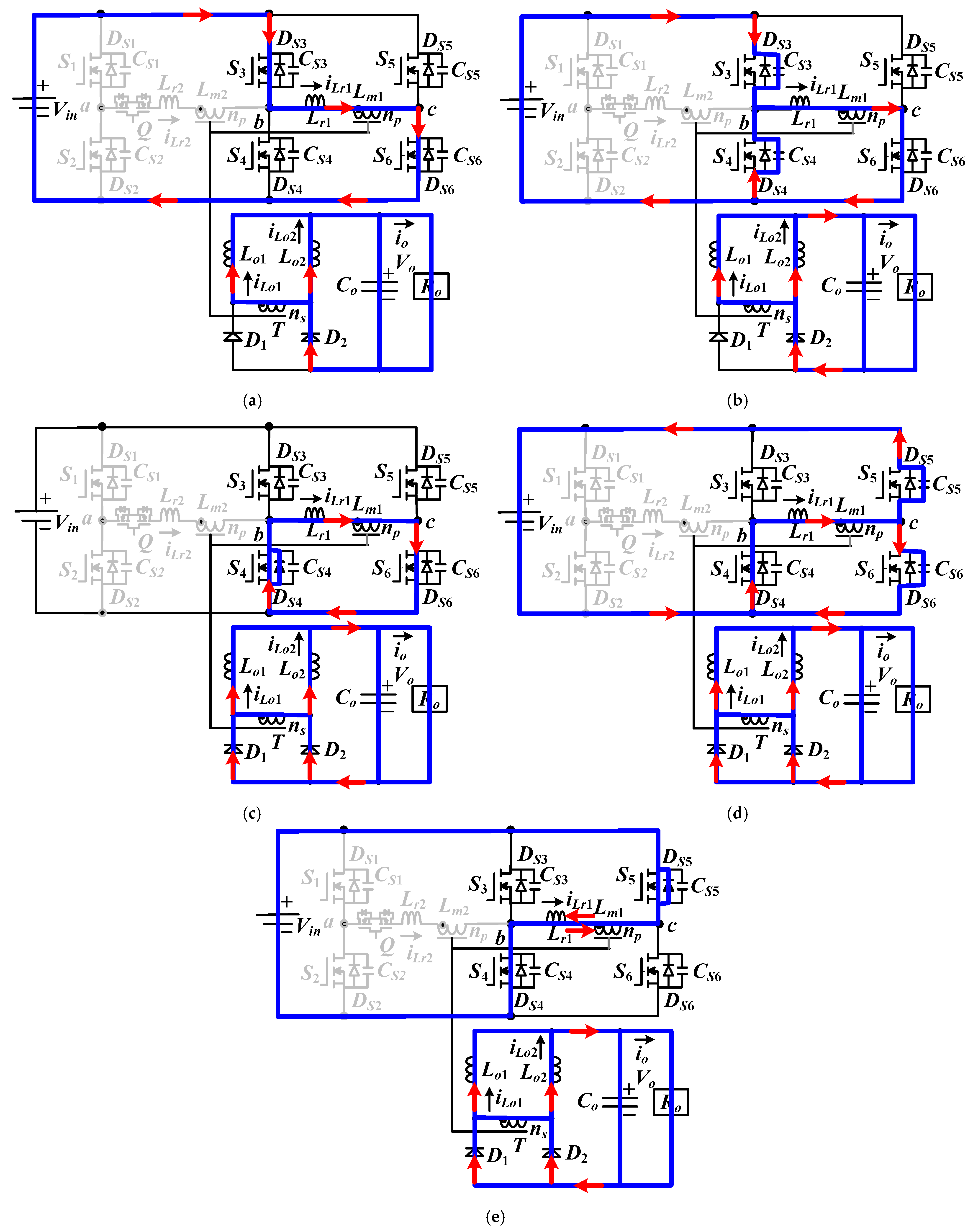
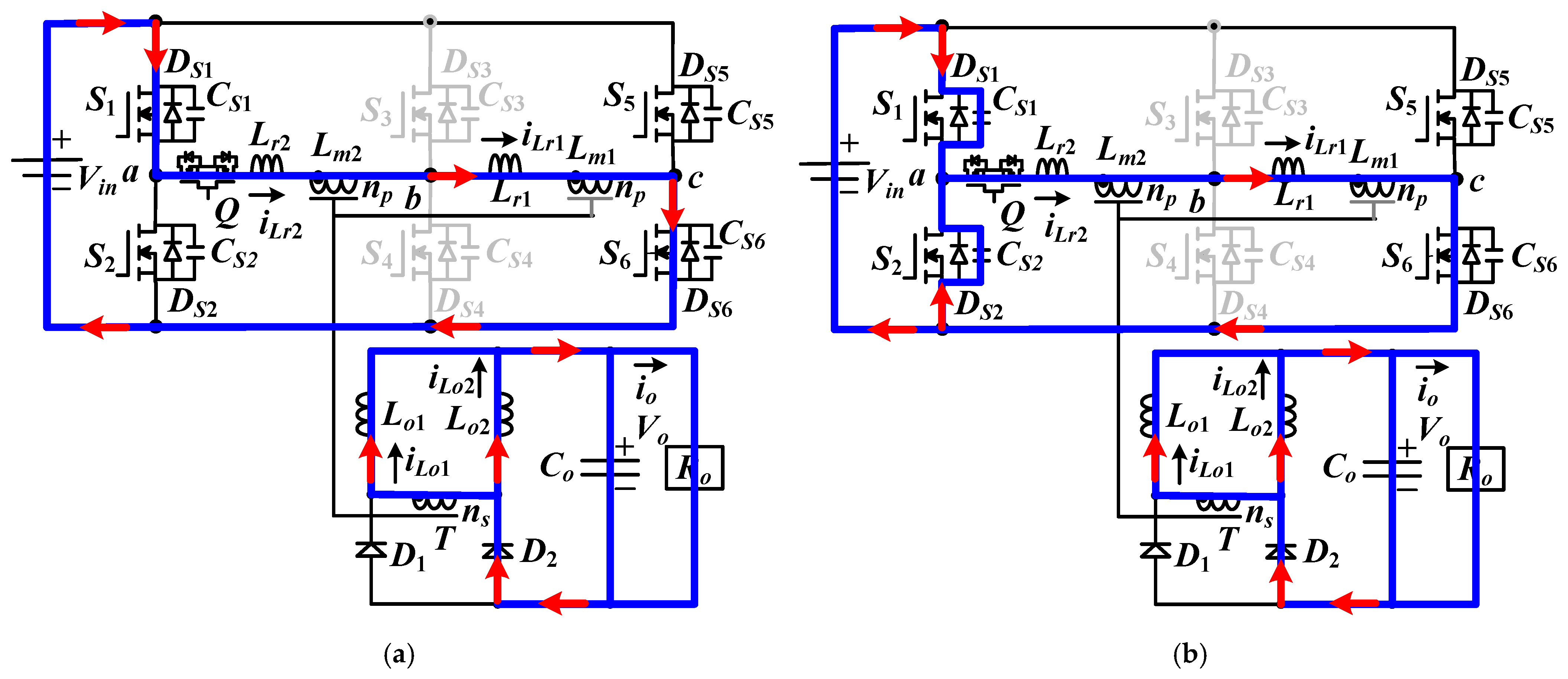
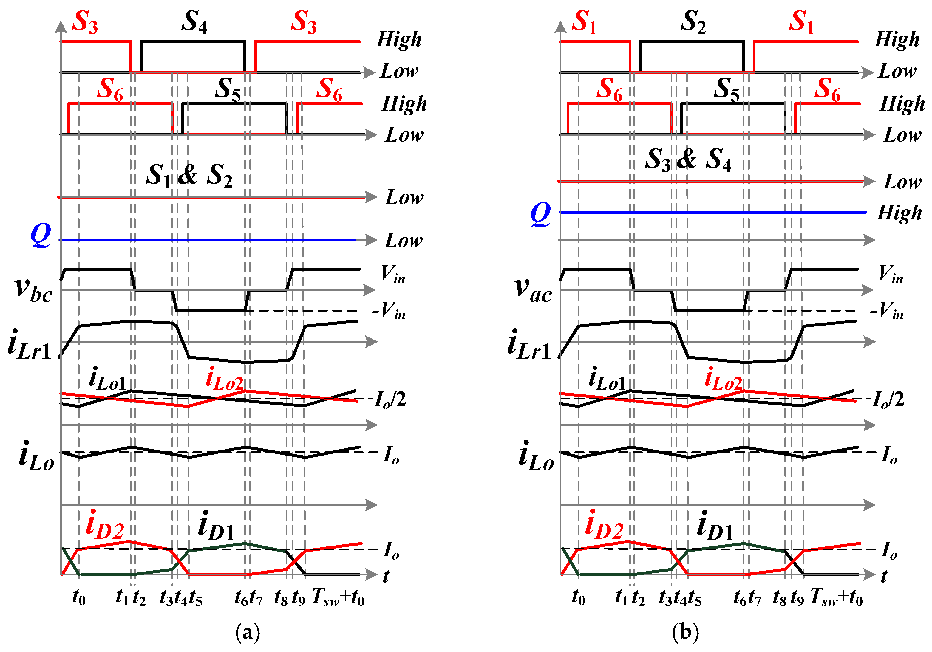
3. Principle of Operation

The converter has two sub-circuits shown in Figure 1b,c for low voltage input Vin,L and high voltage input Vin,H operations. For the low voltage input region (Vin,minVin,L < 2.3Vin,min) in Figure 1b, Q, S2 and S1 are turned OFF and S3–S6 are active with duty cycle control. The transformer turns ratio is NL = np/ns. The corresponding PWM waveforms are provided in Figure 2a. For the high voltage input region (2.3Vin,minVin,H < 5Vin,min) in Figure 1c, Q is ON and S3 and S4 are OFF. S1, S2, S5, and S6 are active with duty cycle control. The transformer turns ratio is NH = 2np/ns. It is assumed the magnetizing inductances Lm1 = Lm2 = Lm >> Lr1 = Lr2 = Lr and the output capacitances CS1 = ... = CS6 = Coss. The PWM waveforms under the high voltage input condition are given in Figure 2b.
According to the PWM waveforms of S3–S6 and the conducting states of D1 and D2, ten operating steps can be observed in Figure 2a under the low voltage input case. As can be observed, the PWM waveforms are symmetric for each half cycle. Thus, only the first five operating steps are explained briefly, and the corresponding step circuits are given in Figure 3.
Step 1 [t0, t1]: At t0, iD1 = 0. S3 and S6 are active in this step. The leg voltage is vbc = Vin, vLo1 = Vin/NL − Vo, and vLo2 = −Vo. Therefore, iLo1 will increase and iLo2 will decrease in this step. The primary and secondary inductor currents are given in Equations (1)–(3).
i L r 1 ( t ) i L r 1 ( t 0 ) + V i n N L V o N L 2 L o 1 ( t t 0 )
i L o 1 ( t ) i L o 1 ( t 0 ) + V i n / N L V o L o 1 ( t t 0 )
i L o 2 ( t ) i L o 2 ( t 0 ) V o L o 2 ( t t 0 )
Step2 [t1, t2]:S3 turns OFF at time t1. iLr1(t1) is positive and CS4 is discharged. CS4 can be discharged to zero at t2 if Equation (4) is satisfied. Therefore, the ZVS operation of S4 is achieved.
( L r + N L 2 L o ) i L r 1 2 ( t 1 ) 2 C o s s V i n 2
The time Δt12 in this step is expressed in Equation (5).
Δ t 12 2 V i n C o s s N L / i L o 1 ( t 1 )
where i L o 1 ( t 1 ) i L o 1 ( t 0 ) + ( V i n / N L V o ) d e f f T s w / L o 1 .
Step 3 [t2, t3]: At t2, vCS4 = 0 and DS4 is conducting due to iLr1 > 0. Thus, the ZVS turn-on operation of S4 can be naturally realized. Due to leg voltage vbc = 0, D1 and D2 are both conducting. It can be observed that vLo1 = vLo2 = −Vo and vLr1 = -vS4,dpvS6,dp, where vS4,dp and vS6,dp are voltage drops on S4 and S6. In step 3, iLo1, iLo2 and iLr1 all decrease, iD1 increases and iD2 decreases.
Step4 [t3, t4]: At t3, S6 is turned off. iLr1 will charge CS6 and discharge CS5. The ZVS turn-on condition of S5 is given in Equation (6).
L r i L r 1 2 ( t 3 ) 2 C o s s V i n 2
Step 4 ends at t4 when vCS5 = 0. The time Δt34 in this step can be obtained in Equation (7).
Δ t 34 2 V i n C o s s / i L r 1 ( t 3 )
Step 5 [t4, t5]: At t4, vCS5 = 0. Then DS5 is conducting due to iLr1(t4) > 0. The ZVS operation of S5 is naturally realized. In step 5, the leg voltage vbc =Vin and D1 and D2 are still conducting. The inductor voltage vLr1 = −Vin. The output filter inductor voltages vLo1 = vLo2 = -Vo. Therefore, inductor currents iLo1, iLo2, and iLr1 all decrease. Step 5 ends at t5 when iD2 = 0. The time duration Δt45 is derived as Equation (8):
Δ t 45 ( I o L r ) / ( V i n N L )
The duty loss in this step can be derived in Equation (9).
d 5 ( I o L r f s w ) / ( V i n N L )
where fsw is the switching frequency. Then, the circuit operation will go to next half switching cycle at time t5.
For high voltage input operation (2.3Vin,minVin,H < 5Vin,min), ac switch Q is ON and active devices S4 and S3 are OFF. Then, the full-bridge converter with switches S1, S2, S5, and S6, as shown in Figure 1c, is operated with duty cycle control. The transformer turns ratio on this equivalent circuit becomes NH = 2np/ns. The dc gain can be expressed as Vo/Vin,Hdeff/NH. This can be observed in Figure 2b. The converter has five steps in one-half of the switching period. The corresponding step circuits are given in Figure 4, and the circuit operations are explained briefly in the following discussions.
Step 1 [t0, t1]: The current iD1 = 0 at t0. Thus, D1 is OFF. In step 1, S1 and S6 are conducting, vac = Vin, vLo1 = Vin/NHVo, and vLo2 = −Vo. The currents iLr1 and iLo1 increase and iLo2 decreases. Step 1 ends at t1 when S1 turns off.
Step2 [t1, t2]:S1 is turned off at t1. iLr1 = iLr2 > 0 and CS2 (CS1) is discharged (charged) by iLr2. The ZVS turn-on operation of S2 is expressed as Equation (10):
( 2 L r + N H 2 L o ) i L r 2 2 ( t 1 ) 2 C o s s V i n 2
Step 3 [t2, t3]:vCS2(t2) = 0. iLr2 > 0 and DS2 is forward biased. At this moment, S2 is turned ON under zero voltage. The leg voltage vac = 0 and both diodes D1 and D2 conducting. Therefore, vLo1 = vLo2 = −Vo and vLr1 + vLr2 = −vS2,dropvS6,dropvQ,drop. The currents iLo1, iLo2, iLr1, and iD2 decrease and iD1 increases.
Step4 [t3, t4]:S6 turns OFF at t3. iLr1 charges (discharges) CS6 (CS5). The ZVS turn-on condition of S5 is obtained as Equation (11):
2 L r i L r 2 2 ( t 3 ) 2 C o s s V i n 2
This step ends at t4 when CS5 is discharged to zero voltage.
Step 5 [t4, t5]:vCS5(t4) = 0. Since iLr1(t4) is positive, DS5 becomes forward biased. In this step, vac =Vin and D2 and D1 are ON. It can be obtained that vLr1 + vLr2 = −Vin, and vLo2 = vLo1 = −Vo. iLo2, iLo1, and iLr1 all decrease. This step ends at t5 when iD2 = 0. The time Δt45 is obtained as Equation (12):
Δ t 45 ( 2 I o L r ) / ( V i n N H )
The duty loss can be calculated in Equation (13).
d 5 ( 2 I o L r f s w ) / ( V i n N H )
At t5, the circuit operation will go to the next half switching period.

4. Steady State Analysis

In relation to the ON/OFF status of Q and S1S6, two equivalent sub-circuits shown in Figure 1 are operated to have a wide voltage input operation and a ZVS turn-on operation. According to the voltage-second balance on Lo1 or Lo2, the load voltage Vo can be expressed as Equation (14):
V o = { n s V i n , L n p ( d n s I o L r f s w n p V i n , L ) V D ,   V i n , min V i n , L < 2.3 V i n , min n s V i n , H 2 n p ( d n s I o L r f s w n p V i n , H ) V D ,   2 . 3 V i n , min < V i n , L 5 V i n , min
where d is the duty cycle on voltage vac or vbc. For the low voltage input condition, NL = np/ns is obtained as Equation (15):
N L = V i n , L ( V o + V D ) ( d I o L r f s w N L V i n , L )
The winding turns of transformer T are expressed as n p ( V i n , min d max T s w ) / ( Δ B A e ) and n s = n p / N L . If the duty loss in (9) is defined, Lr1 and Lr2 can be approximated as Equation (16):
L r = L r 1 = L r 2 = N L d 5 V i n f s w I o
In the presented circuit, the load current is equally distributed on inductors Lo1 and Lo2, and ILo1 = ILo2 = Io/2. If the ripple currents of Lo1 and Lo2 are identical (i.e., ΔiLo1 = ΔiLo1 = ΔiLo), then Lo1 = Lo2 = Lo can be calculated in Equation (17).
L o = ( V o + V D ) Δ i L o f s w ( 1 d + n s I o L r f s w n p V i n , L )
Then, the winding turns of Lo1 and Lo2 are obtained as n L o [ L o ( I o + Δ i L o ) / 2 ] / ( B max A e ) . The peak switch currents are approximated as Equation (18):
i S x , p a e k ( I o + Δ i L o ) / 2 N L + Δ i L m 2 = ( I o + Δ i L o ) / 2 N L + d V i n , L T s w 2 L m L r I o 2 N L L m
where x = 1~6. From the ZVS conditions in (4) and (6), the ZVS operation of leading-leg switches are easier to achieve than lagging-leg switches under the given inductance Lr1. The necessary inductances Lr1 = Lr2 = Lr2 are derived as L r 2 C o s s V i n 2 / i L r 1 2 ( t 3 ) to achieve the ZVS operation of lagging-leg switches S5 and S6. The voltage stress of S1S6 and Q is Vin,max. The voltage stress and dc currents of D2 and D1 are obtained as Vin,max/NL and Io/2, respectively.

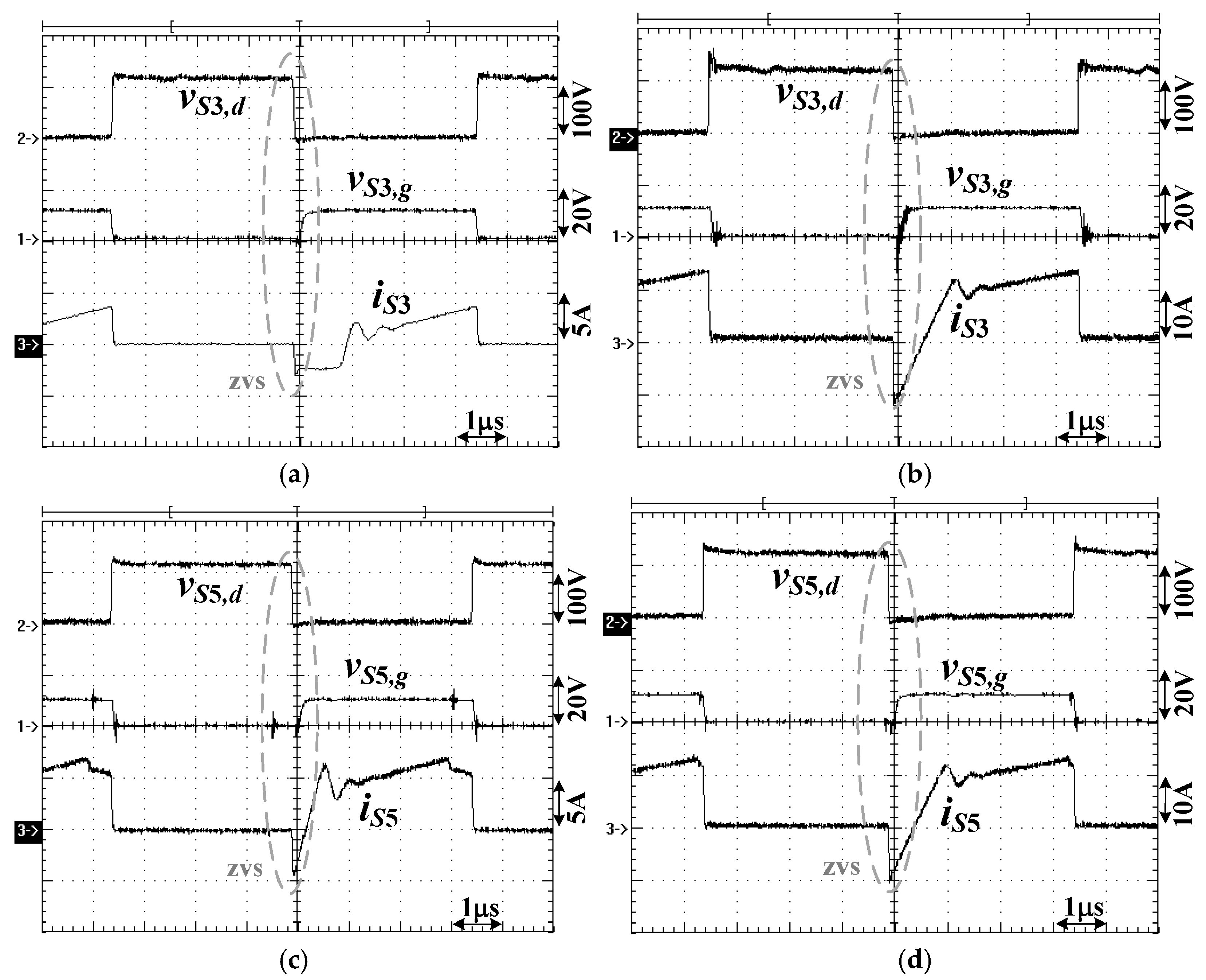
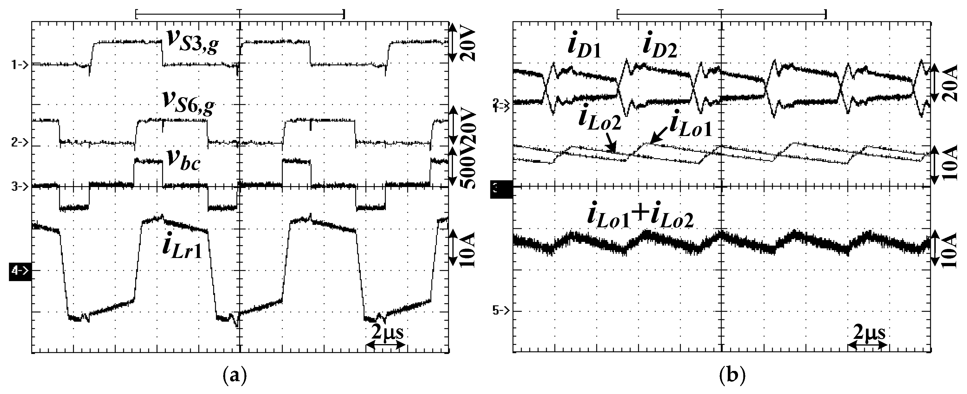
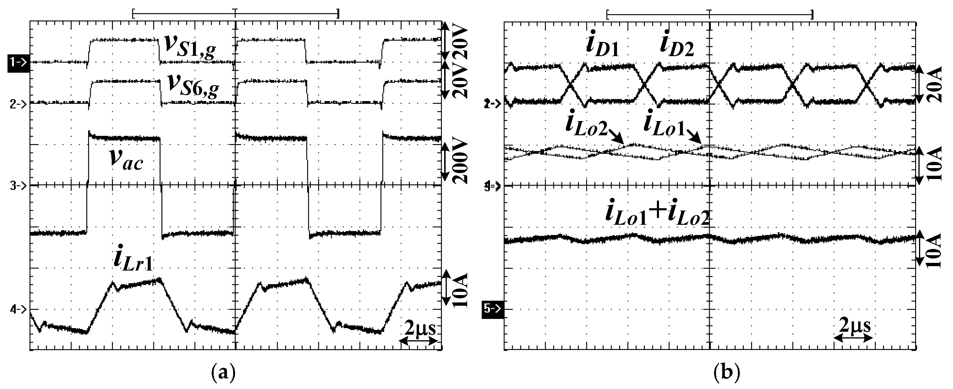
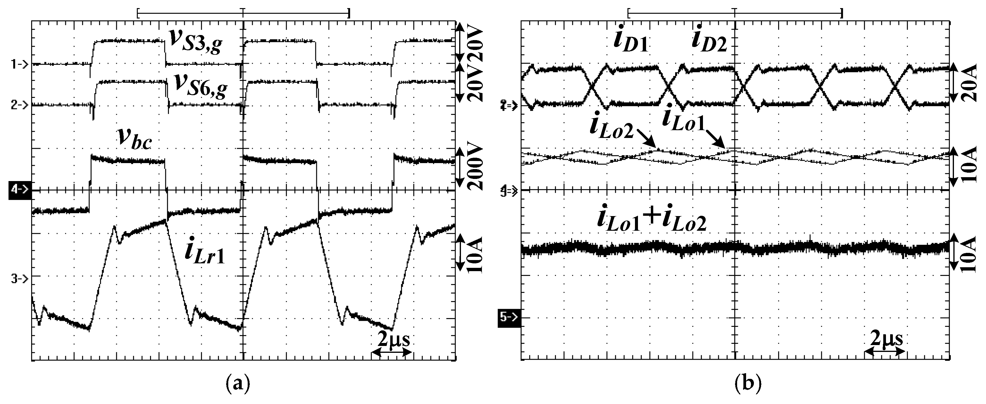
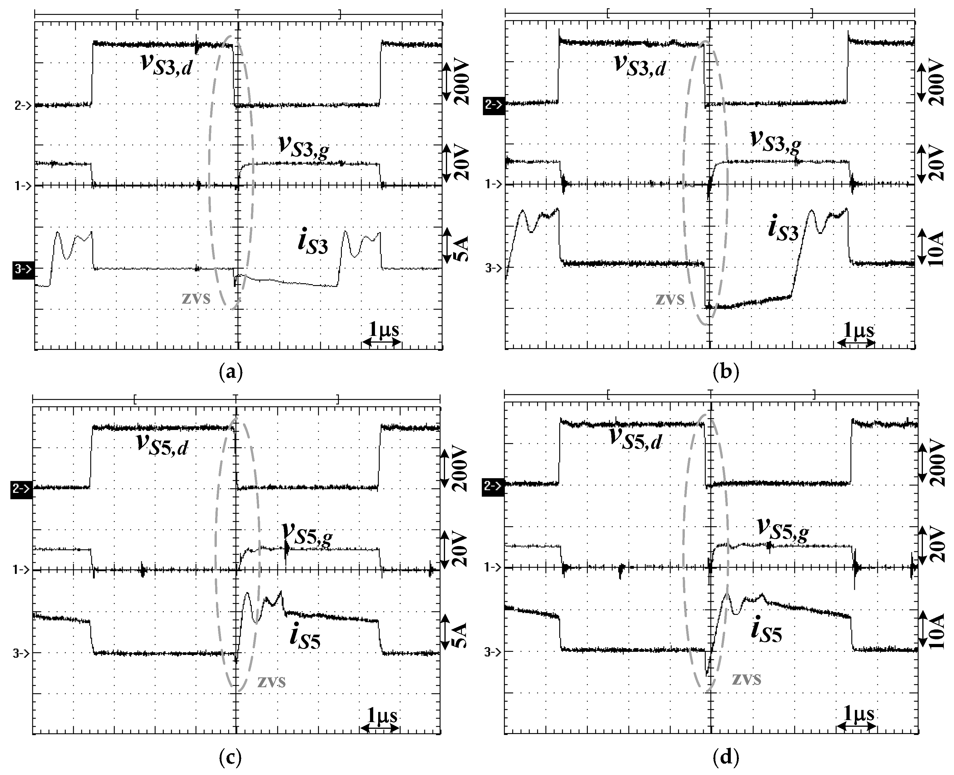
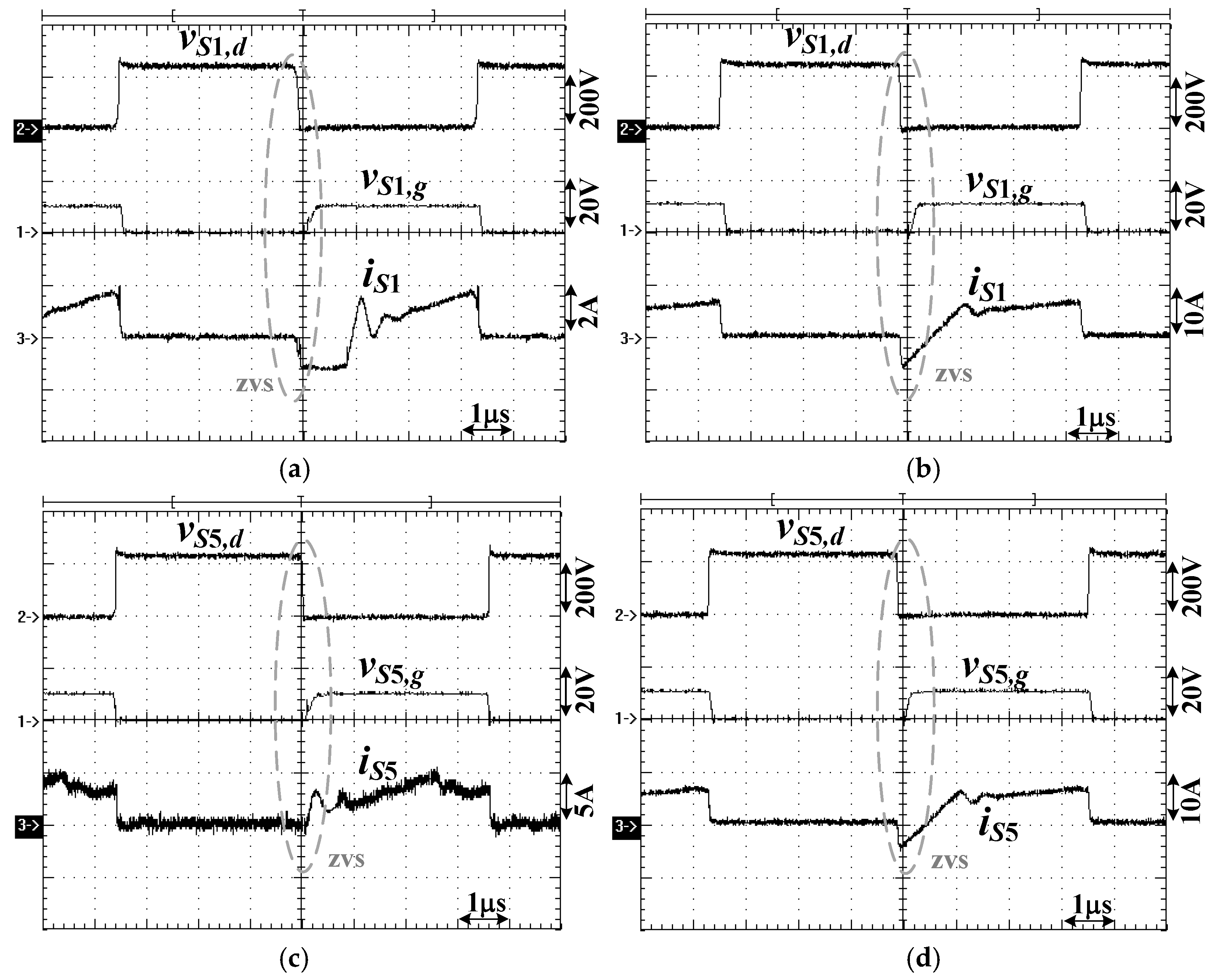
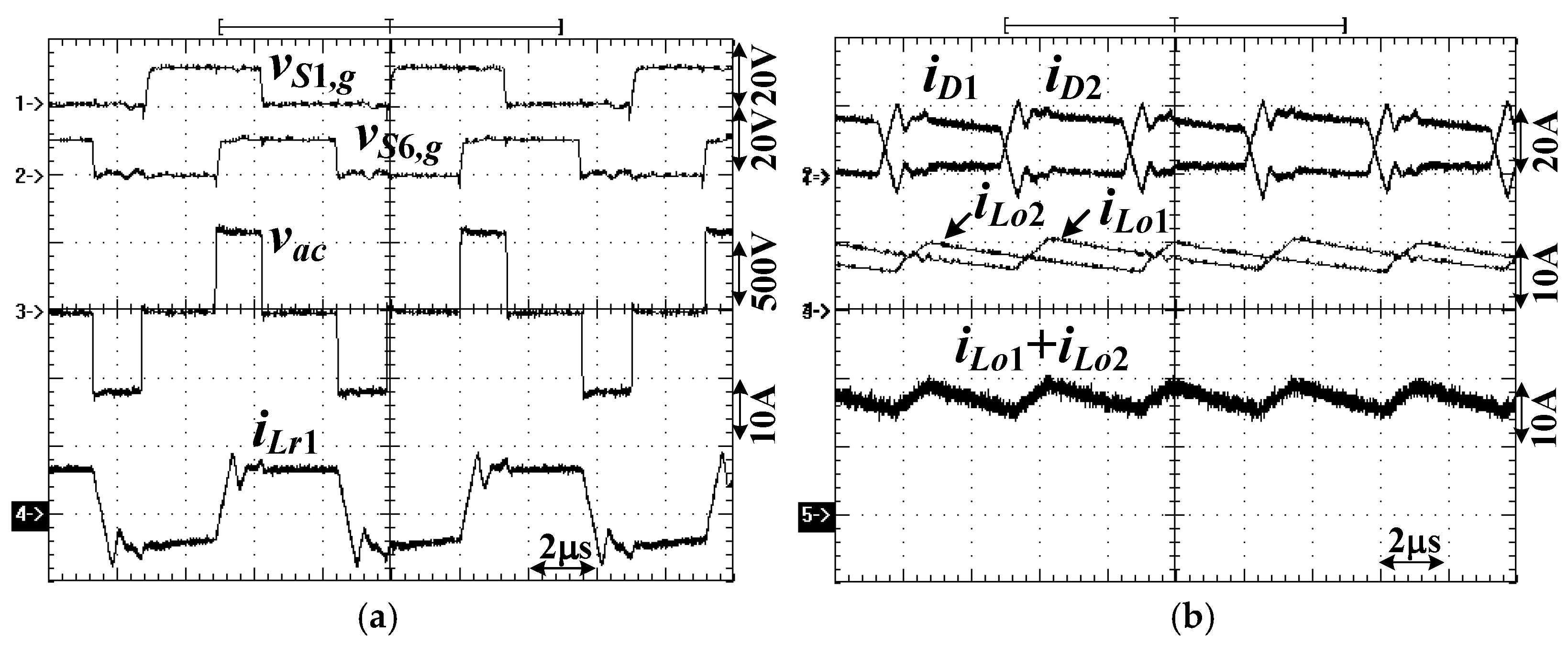
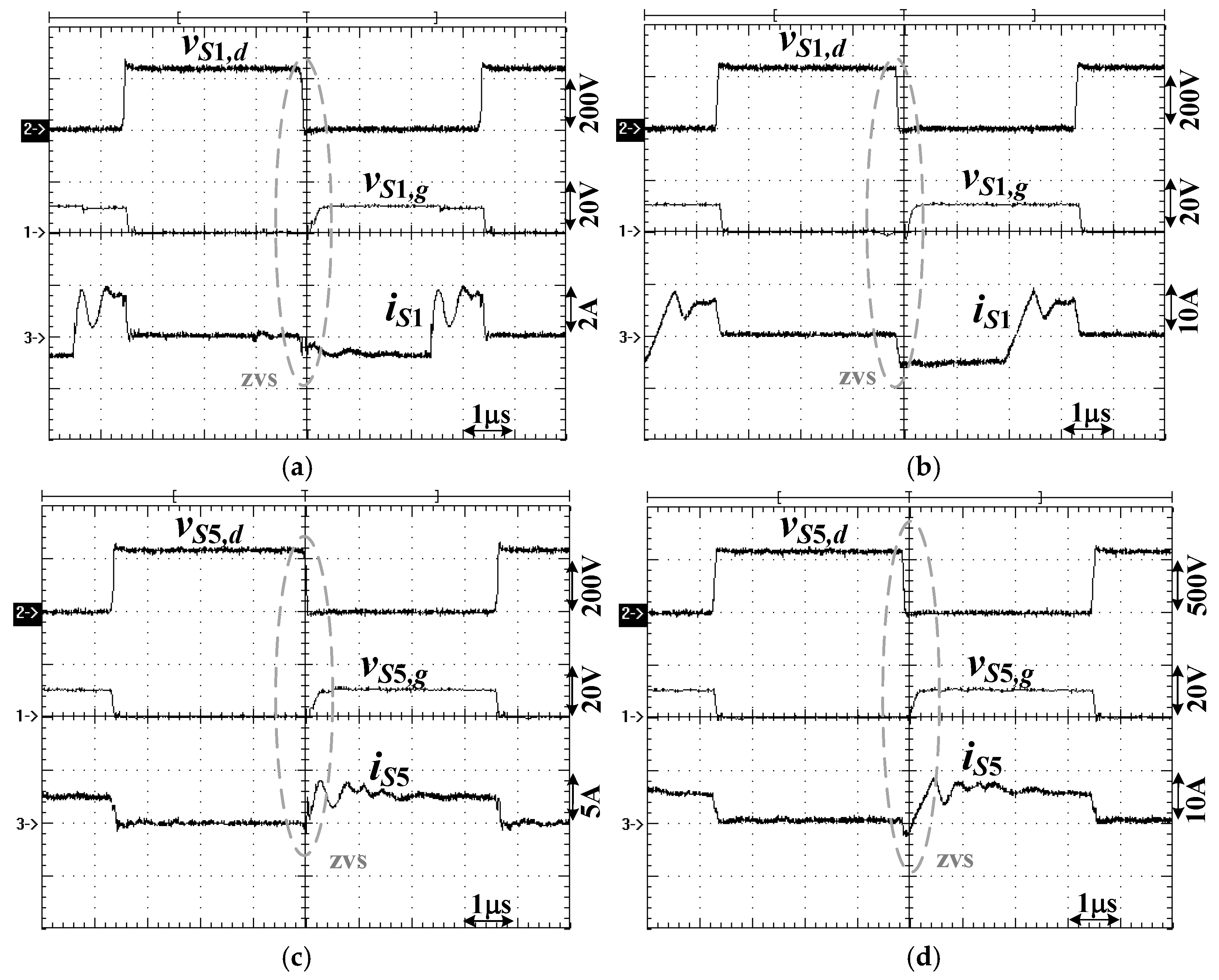
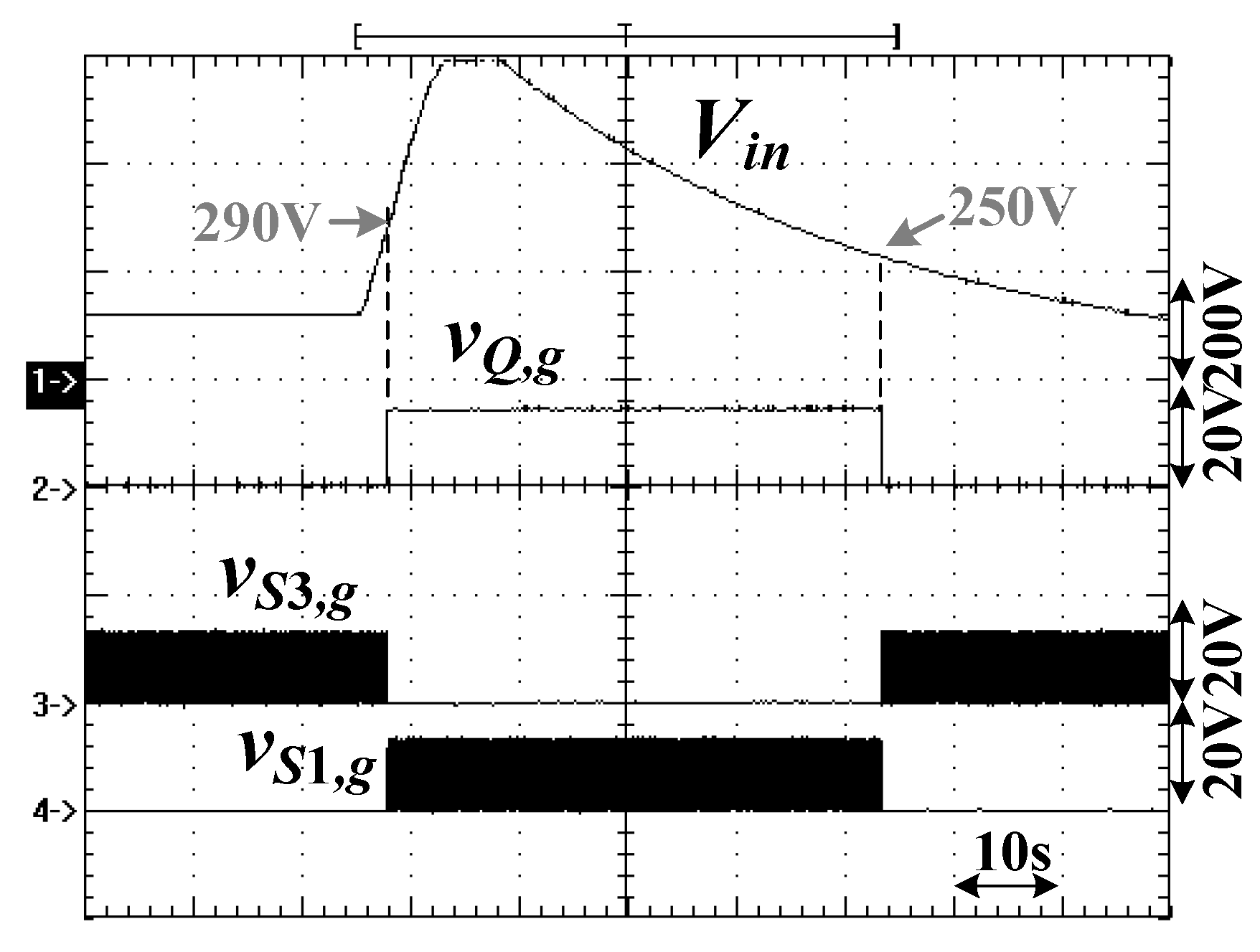
5. Experimental Results

The performance of the converter is confirmed from a laboratory circuit with 800 W rated power. The electric specifications of the test circuit are Vin = 120–600 V, the output voltage Vo = 48 V, the maximum power Po = 800 W, and fsw = 140 kHz. The presented converter operates in the low voltage input condition if 120 V ≤ Vin < 270 V. Then, Q, S1, and S2 are OFF. Likewise, the presented converter operates in the high voltage condition if 270 V < Vin ≤ 600 V. For the high voltage input operation, S3 and S4 are OFF and Q is ON. A Schmitt trigger circuit with ±20 V voltage tolerance is selected to avoid control signal oscillation at the transition voltage 270 V. Therefore, the actual low and high voltage input ranges are Vin,L = 120–290 V and Vin,H = 250–600 V. Figure 5a gives the circuit parameters of a prototype circuit. The phase-shift PWM integrated circuit UCC3895 is selected to produce the gating waveforms of S5 and S6. The gating waveforms of S1S4 are generated by the logic gates and PWM output of UCC3895. Figure 5b gives the picture of the prototype circuit in the laboratory test.
The experimental waveforms of the proposed converter at a low voltage input range (Vin = 120~290 V) are given in Figure 6, Figure 7, Figure 8 and Figure 9. The measured results under a high voltage input range (Vin = 250~600 V) are given in Figure 10, Figure 11, Figure 12 and Figure 13. Figure 6 provides the experimental primary-side (Figure 6a) and secondary-side (Figure 6b) waveforms at Vin = 120 V and Po = 800 W. Note that the duty cycle on voltage vbc is close to 0.5, the ripple current on iLo1 + iLo2 is reduced compared to the ripple current on iLo1 or iLo2, and the resultant current iLo1 + iLo2 has twice the switching frequency of currents iLo1 and iLo2. Figure 7a,b gives the PWM signal of S3 at 20% power and 100% power with the Vin = 120 V input case. In the same way, the PWM waveform of S5 (lagging-leg switch) at 50% and 100% loads are illustrated in Figure 7c,d. Figure 8 and Figure 9 provide the measured results of the presented converter operated at Vin = 290 V in the low voltage input region. Since the higher input voltage will result in a lower duty cycle, it is clear that the voltage vbc at Vin = 290 V input has less duty ratio than in the Vin = 120 V input condition. It can also be noted in Figure 6b and Figure 8b that iLo1 + iLo2 has more ripple current at Vin = 290 V than Vin = 120 V. Figure 9 gives the experimental waveforms of S3 in leading leg and S5 in lagging leg in the 290 V input condition. It can be observed from Figure 7 and Figure 9 that the ZVS turn-on operation of S3 is realized from 20% power for both 120 V and 290 V input conditions. Likewise, the ZVS turn-on operation of S5 is accomplished from 50% power under 120 V and 290 V input cases. For a high voltage input range (Q is ON and S3 and S4 are OFF), the test results are shown in Figure 10, Figure 11, Figure 12 and Figure 13. For Vin = 250 V, the experimental results at 100% power are given in Figure 10. The PWM signals of S1 and S5 are given in Figure 11. In the same way, the experimental waveforms for Vin = 600 V input are given in Figure 12 and Figure 13. From the experimental results in Figure 7, Figure 9, Figure 11 and Figure 13, it can be observed that the leading-leg switch, such as S1 and S3, can achieve ZVS operation from 20% load, and the ZVS operation of S5 in the lagging leg is from 50% power. The measured results of Vin, vQ,g, vS1,g, and vS3,g between 120V and 600 V input are shown in Figure 14. When Vin is increased from 120 V to 290 V, the presented circuit is controlled in the low voltage input range. Q, S1, and S2 are OFF and S3 and S4 are controlled with the phase-shift PWM approach. When Vin > 290 V, Q is ON and S3 and S4 are OFF. S1 and S2 are operated with duty cycle control. When Vin is decreased from 600 V to 250 V, the converter is controlled in the high voltage input range. The switch Q is ON and S3 and S4 are OFF. The test results in Figure 14 are in agreement with the theoretical analysis. The test efficiencies of the proposed converter are 89.3% and 91.2% for 120 V and 600 V input cases under a full load. The synchronous rectifiers can be further used on the secondary side to reduce the conduction losses on D1 and D2 and improve the converter efficiency.

6. Conclusions

A ZVS converter with three-leg circuit topology is presented and discussed, and an 800 W prototype is constructed and measured to achieve ZVS operation and a wide voltage input operation. The presented converter is expected to be used for dc converters with wide input-voltage or output-voltage demand such as dc wind power applications, battery charger systems with wide voltage operation, and solar PV panel power units with variable input voltage. The proposed converter with a phase-shift PWM scheme can be operated at two equivalent circuits. Therefore, active devices in the leading leg are easily turned on under zero voltage. The current doubler rectification circuit is operated on the low-voltage side in order to have less output ripple current. Compared to conventional phase-shift PWM converters, the studied circuit topology has a wider voltage input capability with the drawback of using an extra three switches in the presented converter. Finally, test results with an 800 W prototype are provided to demonstrate circuit characteristics and the validity of the operating principle.

Author Contributions

Conceptualization, methodology, investigation, visualization, writing—original draft, writing—review and editing, B.-R.L.; validation, Y.-H.P. All authors have read and agreed to the published version of the manuscript.

Funding

This research is supported by the Ministry of Science and Technology (MOST), Taiwan, under grant number MOST 108-2221-E-224-022-MY2.

Acknowledgments

The authors are grateful to all of the editors and reviewers for their valuable suggestions to improve this paper.

Conflicts of Interest

The authors declare no conflict of interest.

References

  1. Jumani, T.A.; Mustafa, M.W.; Rasid, M.M.; Anjum, W.; Ayub, S. Salp Swarm Optimization Algorithm-Based Controller for Dynamic Response and Power Quality Enhancement of an Islanded Microgrid. Processes 2019, 7, 840. [Google Scholar] [CrossRef] [Green Version]
  2. Nasir, M.; Iqbal, S.; Khan, H.A.; Guerrero, J.M. Sustainable Rural Electrification Through Solar PV DC Microgrids—An Architecture-Based Assessment. Processes 2020, 8, 1417. [Google Scholar] [CrossRef]
  3. Luo, Z.; Zhu, Z.; Zhang, Z.; Qin, J.; Wang, H.; Gao, Z.; Yang, Z. Multi-Time-Scale Rolling Optimal Dispatch for Grid-Connected AC/DC Hybrid Microgrids. Processes 2019, 7, 961. [Google Scholar] [CrossRef] [Green Version]
  4. Sheng, W.; Hong, Y.; Wu, M.; Ji, Y. A Cooperative Control Scheme for AC/DC Hybrid Autonomous Microgrids. Processes 2020, 8, 311. [Google Scholar] [CrossRef] [Green Version]
  5. Jiang, Y.; Jin, X.; Wang, H.; Fu, Y.; Ge, W.; Yang, B.; Yu, T. Optimal Nonlinear Adaptive Control for Voltage Source Converters via Memetic Salp Swarm Algorithm: Design and Hardware Implementation. Processes 2019, 7, 490. [Google Scholar] [CrossRef] [Green Version]
  6. Ali, H.G.; Arbos, R.V.; Herrera, J.; Peláez-Restrepo, J. Non-Linear Sliding Mode Controller for Photovoltaic Panels with Maximum Power Point Tracking. Processes 2020, 8, 108. [Google Scholar]
  7. Lin, B.R. Hybrid dc/dc Converter Based on Dual Three-Level Circuit and Half-Bridge Circuit. IET Power Electron. 2016, 9, 817–824. [Google Scholar] [CrossRef]
  8. Safaee, A.; Jain, P.; Bakhshai, A. A ZVS Pulsewidth Modulation Full-Bridge Converter with a Low rms Current Resonant Auxiliary Circuit. IEEE Trans. Power Electron. 2016, 31, 4031–4047. [Google Scholar] [CrossRef]
  9. Ren, R.; Liu, B.; Jones, E.A.; Wang, F.F.; Zhang, Z.; Costinett, D. Capacitor-Clamped, Three-Level Gan-Based dc-dc Converter with Dual Voltage Outputs for Battery Charger Applications. IEEE J. Emerg. Sel. Top. Power Electron. 2016, 4, 841–853. [Google Scholar] [CrossRef]
  10. Steigerwald, R.L. A Comparison of Half-Bridge Resonant Converter Topologies. IEEE Trans. Power Electron. 1988, 3, 174–182. [Google Scholar] [CrossRef]
  11. Lin, B.R.; Chu, C.W. Hybrid Full-Bridge and LLC Converter with Wide ZVS Range and Less Output Inductance. IET Power Electron. 2016, 9, 377–384. [Google Scholar] [CrossRef]
  12. Lee, J.B.; Kim, J.K.; Baek, J.I.; Kim, J.H.; Moon, G.W. Resonant Capacitor on/off Control of Half-Bridge LLC Converter for High Efficiency Server Power Supply. IEEE Trans. Ind. Electron. 2016, 63, 5410–5415. [Google Scholar] [CrossRef]
  13. Jeong, Y.; Kim, J.K.; Lee, J.B.; Moon, G.W. An Asymmetric Half-Bridge Resonant Converter Having a Reduced Conduction Loss for DC/DC Power Applications with a Wide Range of Low Input Voltage. IEEE Trans. Power Electron. 2017, 32, 7795–7804. [Google Scholar] [CrossRef]
  14. Zhang, Y.; Fu, C.; Sumner, M.; Wang, P. A Wide Input-Voltage Range Quasi-Z-Source Boost DC–DC Converter with High-Voltage Gain for Fuel Cell Vehicles. IEEE Trans. Ind. Electron. 2018, 65, 5201–5212. [Google Scholar] [CrossRef] [Green Version]
  15. Wang, P.; Zhou, L.; Zhang, Y.; Li, J.; Sumner, M. Input-Parallel Output-Series DC-DC Boost Converter with a Wide Input Voltage Range, for Fuel Cell Vehicles. IEEE Trans. Veh. Tech. 2017, 66, 7771–7781. [Google Scholar] [CrossRef]
  16. Wang, X.; Tian, F.; Batarseh, I. High Efficiency Parallel Post Regulator for Wide Range Input DC-DC Converter. IEEE Trans. Power Electron. 2008, 23, 852–858. [Google Scholar] [CrossRef]
  17. Lu, J.; Kumar, A.; Afridi, K.K. Step-Down Impedance Control Network Resonant DC-DC Converter Utilizing an Enhanced Phase-Shift Control for Wide-Input-Range Operation. IEEE Trans. Ind. Appl. 2018, 54, 4523–4536. [Google Scholar] [CrossRef]
  18. Li, W.; Zong, S.; Liu, F.; Yang, H.; He, X.; Wu, B. Secondary-Side Phase-Shift-Controlled ZVS DC/DC Converter with Wide Voltage Gain for High Input Voltage Applications. IEEE Trans. Power Electron. 2013, 28, 5128–5139. [Google Scholar] [CrossRef]
  19. Kim, B.; Kim, S.; Hun, D.Y.; Choi, J.H.; Kim, M. Hybrid Resonant Half-Bridge DC/DC Converter with Wide Input Voltage Range. In Proceedings of the IEEE APEC Conference, San Antonio, TX, USA, 4–8 March 2018; pp. 1876–1881. [Google Scholar]
  20. Hu, H.; Fang, X.; Chen, F.; Shen, Z.J.; Batarseh, I. A Modified High-Efficiency LLC Converter with Two Transformers for Wide Input-Voltage Range Applications. IEEE Trans. Power Electron. 2013, 28, 1946–1960. [Google Scholar] [CrossRef]
  21. Lin, B.R.; Liu, Y.C. Analysis of a Wide Voltage Hybrid Soft Switching Converter. Electronics 2021, 10, 473. [Google Scholar] [CrossRef]
  22. Lin, B.R.; Ko, M.C. Investigation of a hybrid converter with 16:1 wide voltage operation. IET Proc. Electron. Lett. 2021, 57, 74–77. [Google Scholar] [CrossRef]
Figure 1. Proposed converter (a); circuit schematic (b); equivalent sub-circuit under low voltage input range (c); equivalent sub-circuit under high voltage input range.
Processes 09 00580 g001aProcesses 09 00580 g001b
Figure 2. Pulse-width modulation (PWM) singles in the (a) low voltage input range; (b) high voltage input range.
Processes 09 00580 g002
Figure 3. Equivalent circuits under low voltage input condition during the first half switching period: (a) step 1 circuit; (b) step 2 circuit; (c) step 3 circuit; (d) step 4 circuit; (e) step 5 circuit.
Processes 09 00580 g003
Figure 4. Equivalent circuits under high voltage input condition during the first half switching period: (a) step 1 circuit; (b) step 2 circuit; (c) step 3 circuit; (d) step 4 circuit;(e) step 5 circuit.
Processes 09 00580 g004aProcesses 09 00580 g004b
Figure 5. Laboratory prototype: (a) circuit diagram; (b) picture of prototype circuit.
Processes 09 00580 g005
Figure 6. Test waveforms at Vin = 120 V (low voltage input range) and Po = 800 W: (a) primary-side waveforms vS3,g, vS5,g, vbc, and iLr1; (b) secondary-side waveforms iD1, iD2, iLo1, iLo2, and iLo1 + iLo2.
Processes 09 00580 g006
Figure 7. Test waveforms of S3 and S5 at Vin = 120 V (low voltage input range): (a) S3 under 20% load; (b) S3 under 100% load; (c) S5 under 20% load; (d) S5 under 100% load.
Processes 09 00580 g007
Figure 8. Test waveforms at Vin = 290 V (low voltage input range) and Po = 800 W: (a) primary-side waveforms vS3,g, vS5,g, vbc, and iLr1; (b) secondary-side waveforms iD1, iD2, iLo1, iLo2, and iLo1 + iLo2.
Processes 09 00580 g008
Figure 9. Test waveforms of S3 and S5 at Vin = 290 V (low voltage input range): (a) S3 under 20% load; (b) S3 under 100% load; (c) S5 under 20% load; (d) S5 under 100% load.
Processes 09 00580 g009
Figure 10. Test waveforms at Vin = 250 V and Po = 800 W: (a) primary-side waveforms vS1,g, vS5,g, vac, and iLr1; (b) secondary-side waveforms iD1, iD2, iLo1, iLo2, and iLo1 + iLo2.
Processes 09 00580 g010
Figure 11. Test waveforms of S1 and S5 at Vin = 250 V: (a) S1 under 20% load; (b) S1 under 100% load; (c) S5 under 20% load; (d) S5 under 100% load.
Processes 09 00580 g011
Figure 12. Test waveforms at Vin = 600 V and Po = 800 W: (a) primary-side waveforms vS1,g, vS5,g, vac, and iLr1; (b) secondary-side waveforms iD1, iD2, iLo1, iLo2, and iLo1 + iLo2.
Processes 09 00580 g012
Figure 13. Test waveforms of S1 and S5 at Vin = 600 V: (a) S1 under 20% load; (b) S1 under 100% load; (c) S5 under 20% load; (d) S5 under 100% load.
Processes 09 00580 g013
Figure 14. Test waveforms of Vin, vQ,g, vS1,g, and vS3,d under Vin = 120–600 V variation.
Processes 09 00580 g014
Publisher’s Note: MDPI stays neutral with regard to jurisdictional claims in published maps and institutional affiliations.

