
Novel High-Efficiency High Step-Up DC–DC Converter with Soft Switching and Low Component Voltage Stress for Photovoltaic System


Abstract
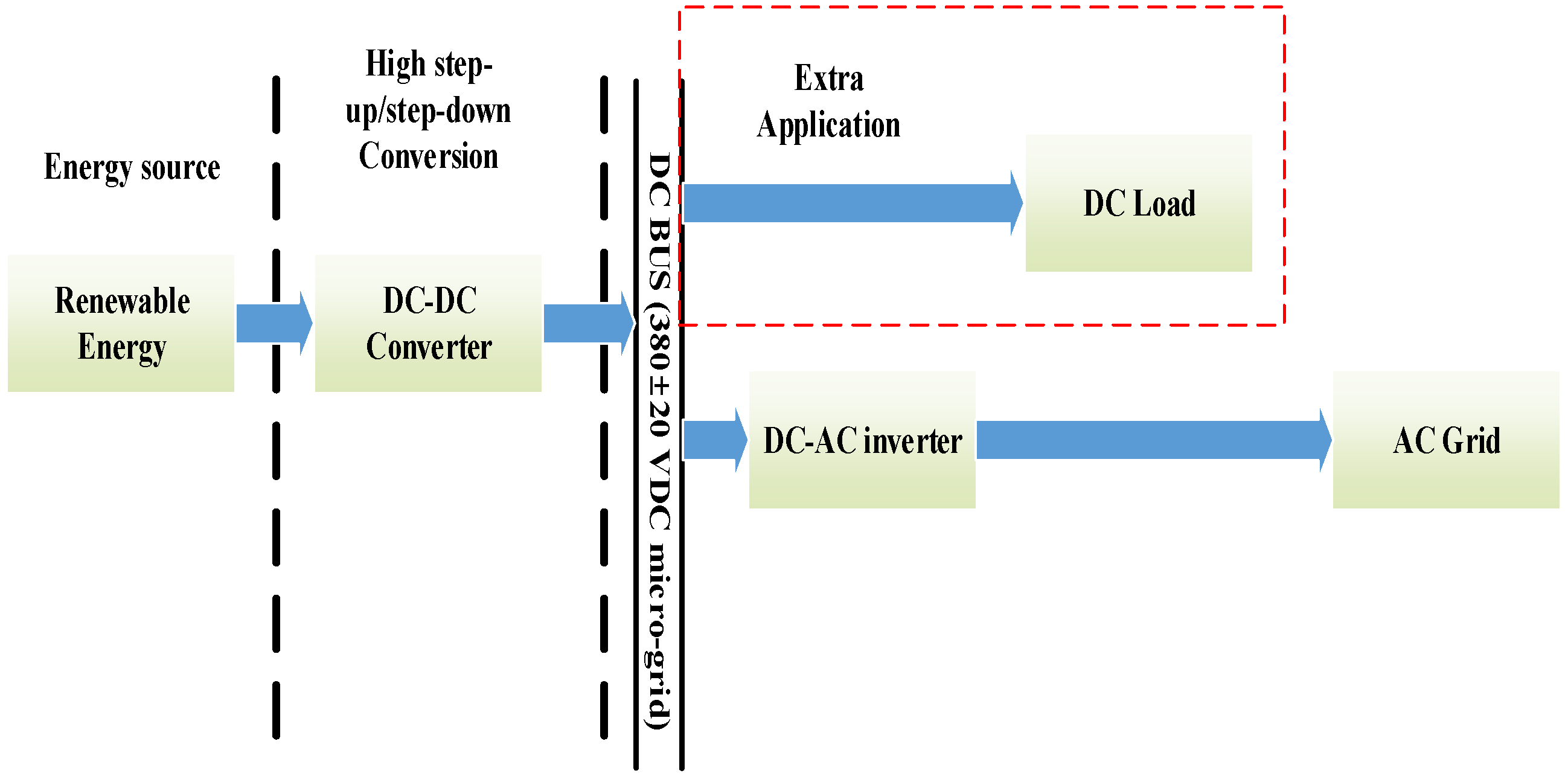
:1. Introduction
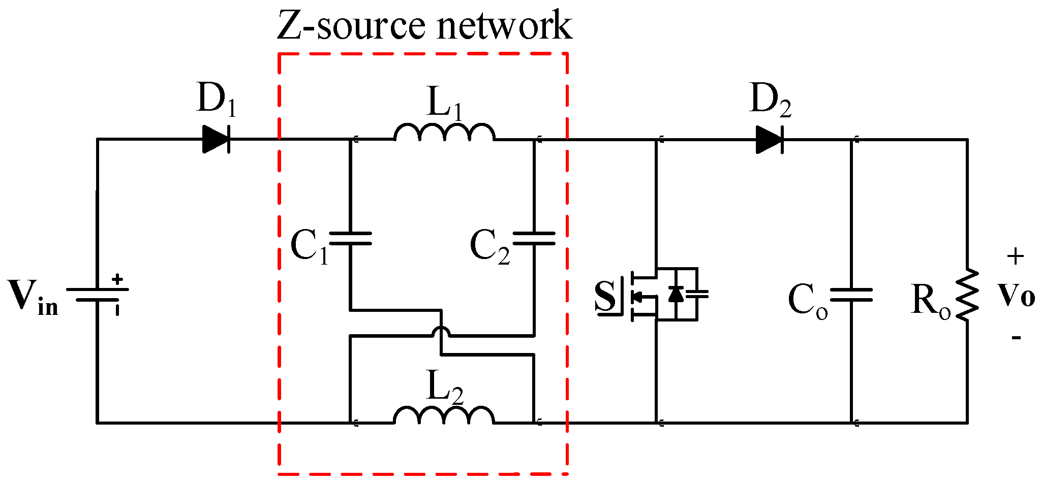
2. Literature Review
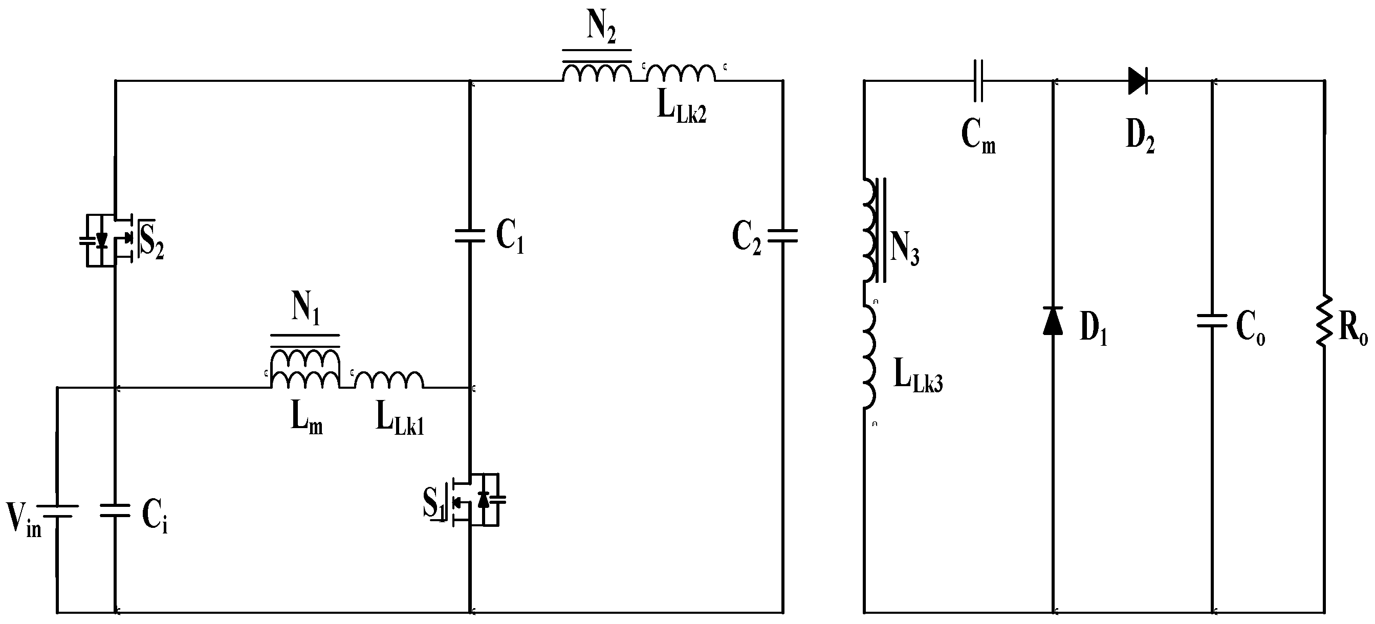
3. Circuit Architecture and Principle of Operation
- (1)
- The parasitic effect and internal resistance, which occur at high frequencies, are absent.
- (2)
- The switches and parasitic diodes of the switches are ideal, and the parasitic capacitance is considered.
- (3)
- The capacitance of C1, C2, Ci, Co, and Cm is infinite.
- (4)
- The leakage inductance values Llk1, Llk2, and Llk3 are much lower than the magnetizing inductance Lm.
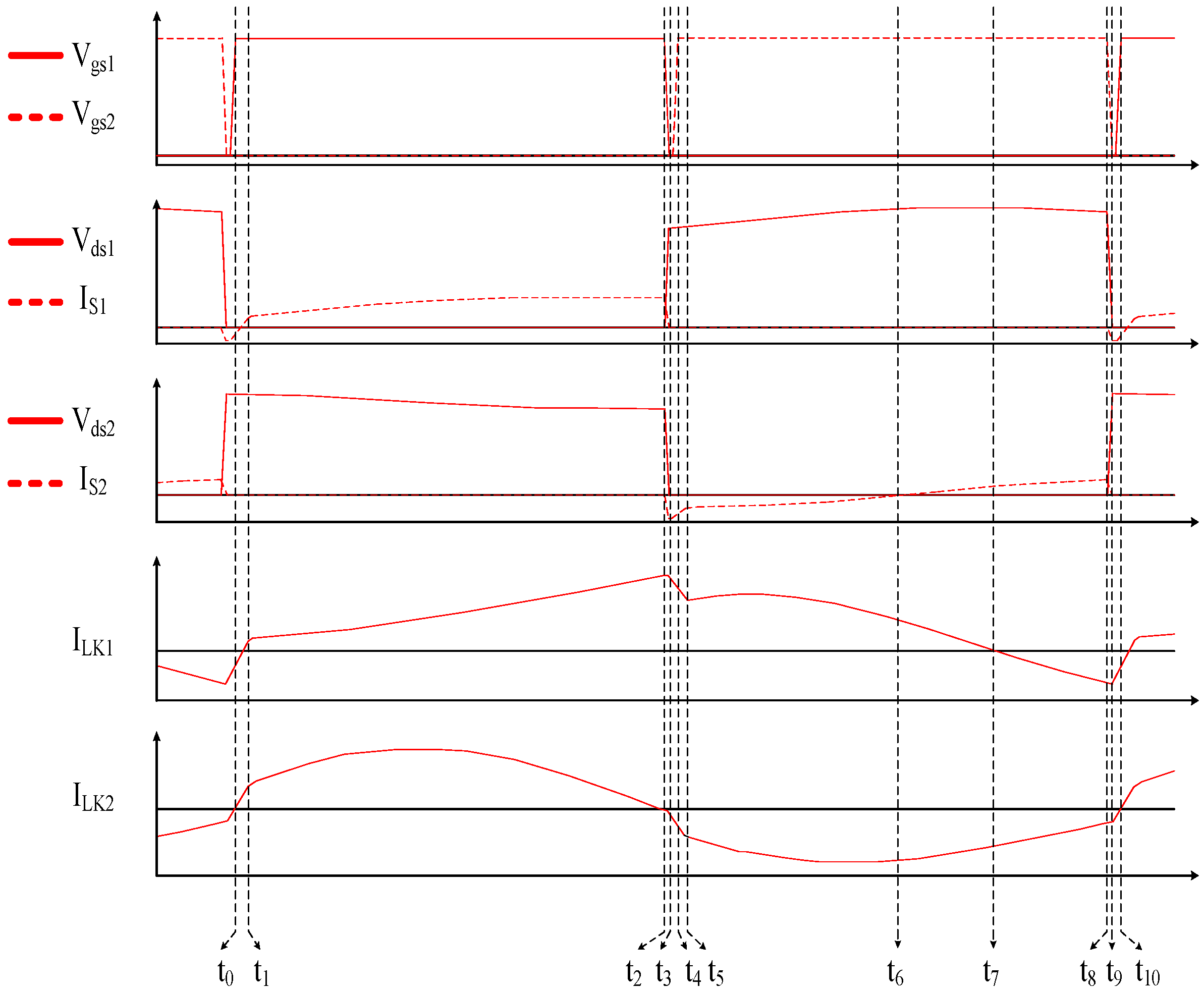
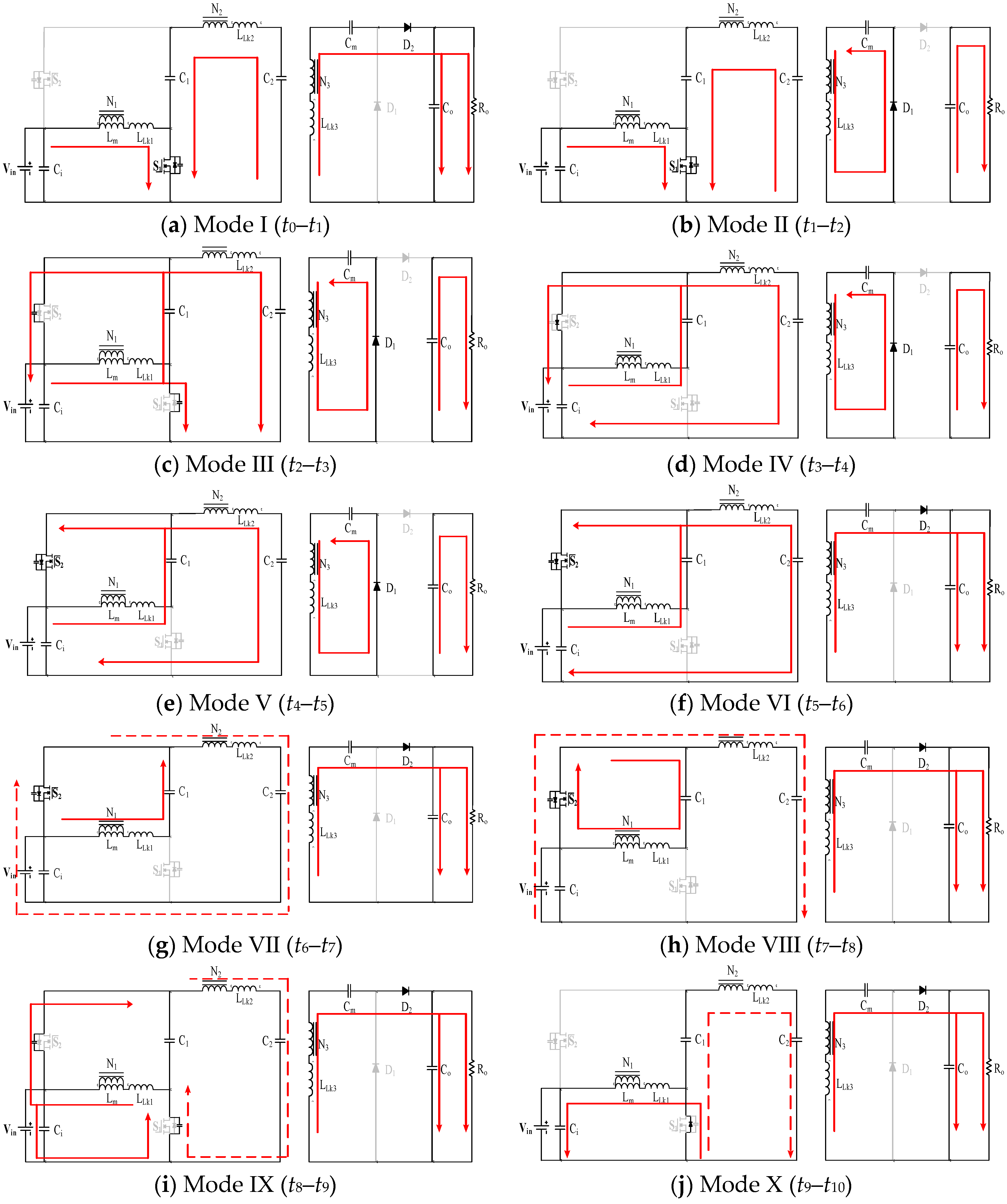
- (1)
- Mode I (t0–t1)
- (2)
- Mode II (t1–t2)
- (3)
- Mode III (t2–t3)
- (4)
- Mode IV (t3–t4)
- (5)
- Mode V (t4–t5)
- (6)
- Mode VI (t5–t6)
- (7)
- Mode VII (t6–t7)
- (8)
- Mode VIII (t7–t8)
- (9)
- Mode IX (t8–t9)
- (10)
- Mode X (t9–t10)
4. Steady-State Analysis
- (1)
- All components are ideal, and the internal resistance and parasitic effects are absent.
- (2)
- The capacitance of all capacitors is infinite, making the voltage of the capacitors constant.
- (3)
- The leakage inductance of the winging inductor is absent.
- (4)
- To make calculations easier, the ideal transformer is represented by , and N is defined as the turns ratio of a transformer.
4.1. Voltage Gain Ratio
4.2. Voltage Stress Analysis of Components
4.3. Literature Comparison
5. Experiential Results
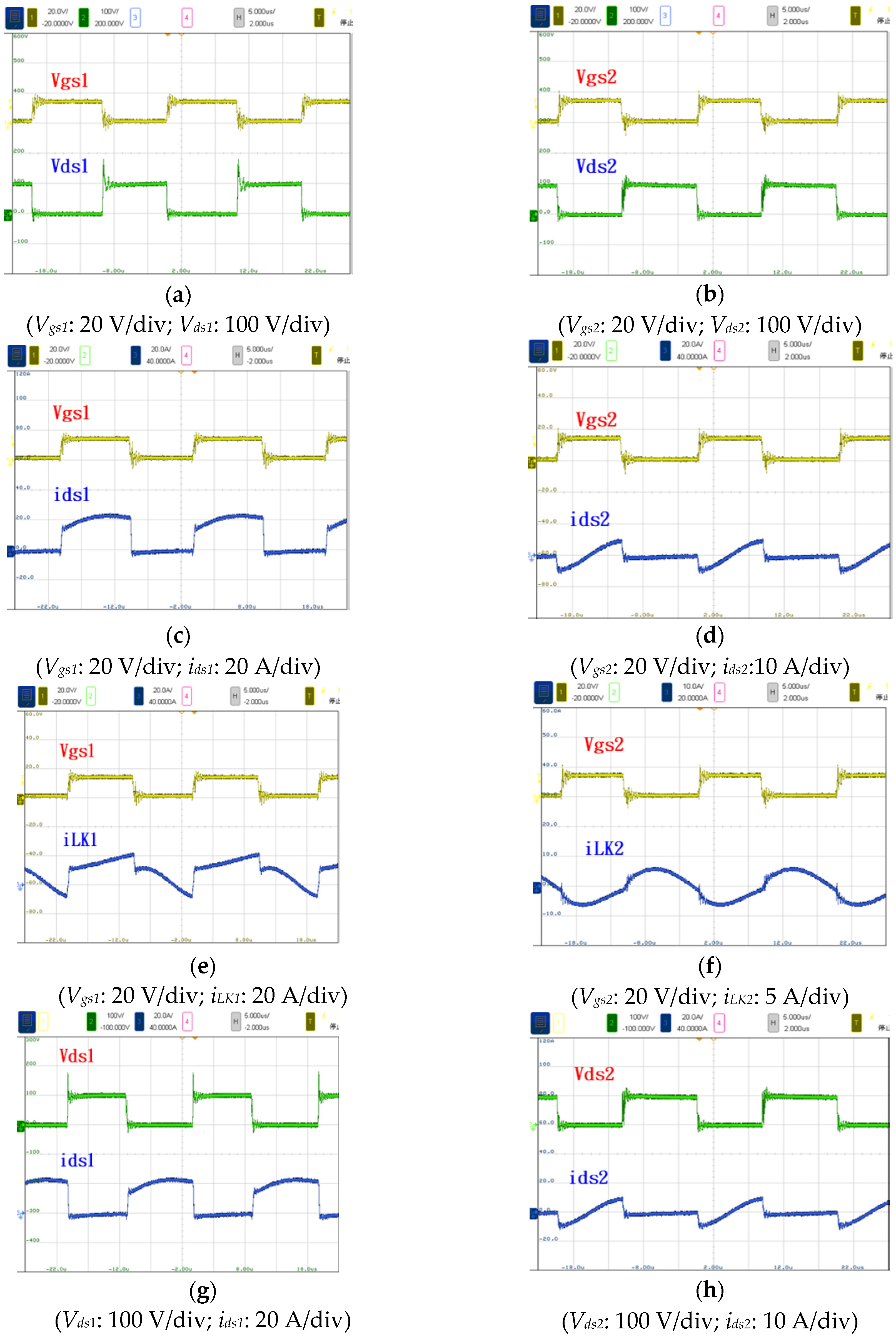
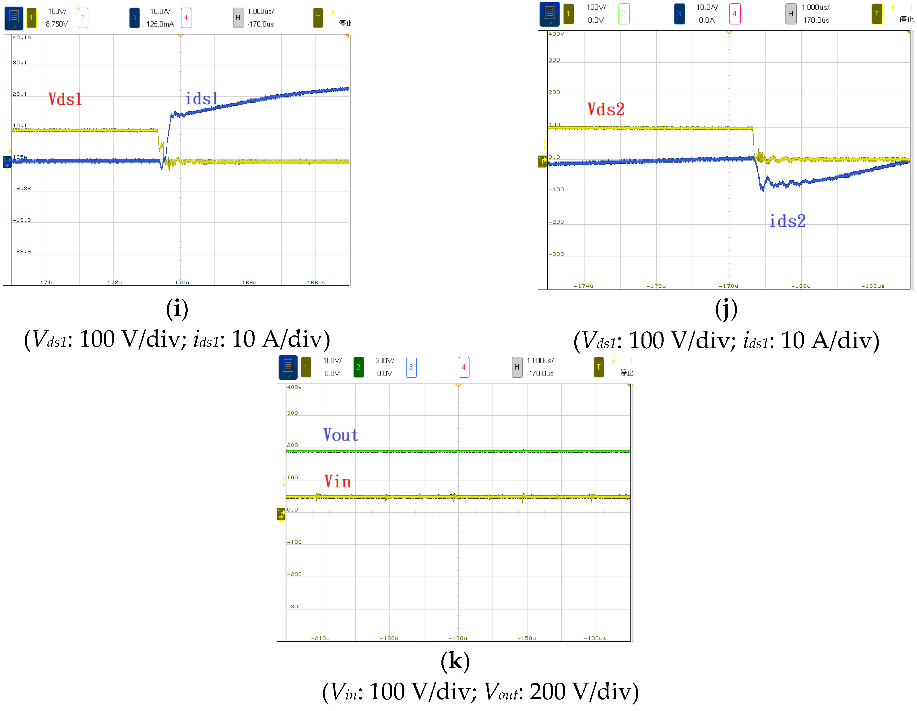
5.1. Experimental Waveforms
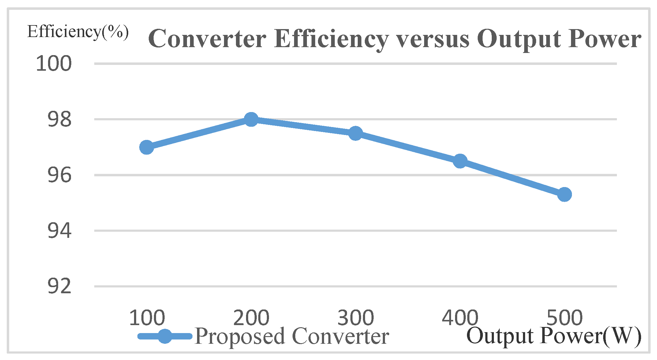
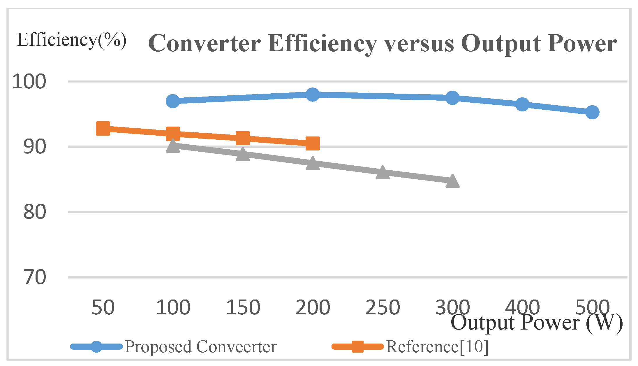
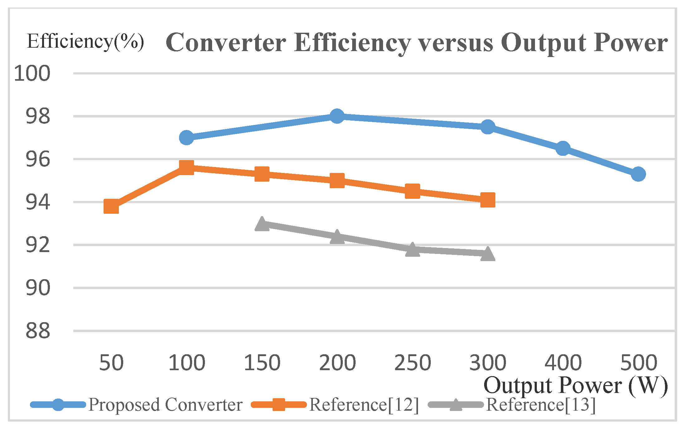
5.2. Measured Efficiency
6. Conclusions
Author Contributions
Funding
Institutional Review Board Statement
Informed Consent Statement
Data Availability Statement
Conflicts of Interest
References
- Information Network. Available online: https://www.moeaboe.gov.tw/ECW/populace/home/Home.aspx (accessed on 22 April 2021).
- Hua, L.W.; Dong, L.X.; Deng, Y.; Liu, J.; He, X. A Review of Non-Isolated High Step-Up DC/DC Converter in Renewable Energy Applications. In Proceedings of the 2009 Twenty-Fourth Annual IEEE Applied Power Electronics Conference and Exposition, Piscataway, NJ, USA, 15–19 February 2009; pp. 364–369. [Google Scholar]
- Luo, F.L. Positive Output Luo Converter, Voltage Lift Technique. IEEE Electr. Power Appl. 1999, 146, 415–432. [Google Scholar] [CrossRef]
- Liu, H.; Hu, H.; Wu, H.-F.; Xing, Y.; Batarseh, I. Overview of High-Step-Up Coupled-Inductor Boost Converters. IEEE J. Emerg. Sel. Top. Power Electron. 2016, 4. [Google Scholar] [CrossRef]
- Vazquez, N.; Estrada, L.; Hernandez, C.; Rodriguez, E. The Tapped-Inductor Boost Converter. In Proceedings of the 2007 IEEE International Symposium on Industrial Electronics, Vigo, Spain, 4–7 June 2007; pp. 538–543. [Google Scholar]
- Yu, W.; Hutchens, C.; Lai, J.-S.; Zhang, J.; Lisi, G.; Djabbari, A.; Smith, G.; Hegarty, T. High efficiency converter with charge pump and coupled inductor for wide input photovoltaic AC module applications. In Proceedings of the 2009 IEEE Energy Conversion Congress and Exposition, San Jose, CA, USA, 20–24 September 2009; pp. 3895–3900. [Google Scholar]
- Wai, R.-J.; Duan, R.-Y. High Step-Up Converter with Coupled-Inductor. IEEE Trans. Power Electron. 2005, 20, 1025–1035. [Google Scholar] [CrossRef]
- Wai, R.-J.; Lin, C.-Y.; Duan, R.-Y. High-efficiency DC-DC converter with high voltage gain and reduced switch stress. IEEE Trans. Ind. Electron. 2007, 54, 354–364. [Google Scholar] [CrossRef]
- Wu, Y.-E.; Huang, K.-C. A single-switch cascaded high step-up voltage converter with 95% maximum efficiency for renewable energy systems. Int. J. Circuit Theory Appl. 2015, 44, 1385–1399. [Google Scholar] [CrossRef]
- Haji, M.M.; Babaei, E.; Sabahi, M. High Step-Up Quasi-Z Source DC–DC Converter. IEEE Trans. Power Electron. 2018, 33, 10563–10571. [Google Scholar] [CrossRef]
- Sharifi, S.; Monfared, M. Modified Series and Tapped Switched-Coupled-Inductors Quasi-Z-Source Networks. IEEE Trans. Ind. Electron. 2019, 66, 5970–5978. [Google Scholar] [CrossRef]
- Evran, F.; Aydemir, M.T. Isolated High Step-Up DC–DC Converter with Low Voltage Stress. IEEE Trans. Power Electron. 2013, 29, 3591–3603. [Google Scholar] [CrossRef]
- Evran, F.; Aydemir, M.T. Z-source-based isolated high step-up converter. IET Power Electron. 2013, 6, 117–124. [Google Scholar] [CrossRef]
- Peng, F. Z-source inverter. Wiley Encycl. Electr. Electron. Eng. 2003, 39, 504–510. [Google Scholar]
- Fang, X. A novel Z-source dc-dc converter. In Proceedings of the 2008 IEEE International Conference on Industrial Technology, Chengdu, China, 21–24 April 2008; pp. 1–4. [Google Scholar]
- Cao, D.; Peng, F.Z. A Family of Z-source and Quasi-Z-source DC-DC Converters. In Proceedings of the 2009 Twenty-Fourth Annual IEEE Applied Power Electronics Conference and Exposition, Washington, DC, USA, 15–19 February 2009; pp. 1097–1101. [Google Scholar]
- Yang, L.; Qiu, D.; Zhang, B.; Zhang, G.; Xiao, W. A quasi-Z-source DC-DC converter. In Proceedings of the 2014 IEEE Energy Conversion Congress and Exposition (ECCE), Pittsburgh, PA, USA, 14–18 September 2014; pp. 941–947. [Google Scholar]
- Suresh, A.; Rashmi, M.R.; Madusuthanan, V.; Kumar, P.V. Closed Loop Control of Bi-Directional Soft Switched Quasi Z-Source DC-DC Converter. Circuits Syst. 2016, 7, 574–584. [Google Scholar] [CrossRef] [Green Version]


| References | Proposed Paper | Reference [10] | Reference [11] |
|---|---|---|---|
| Input voltage | 48 V | 24 V | 40 V |
| Output voltage | 380 V | 365 V | 200 V |
| Output power | 500 W | 200 W | 300 W |
| Number of switches | 2 | 1 | 1 |
| Number of diodes | 2 | 5 | 3 |
| Number of inductors | 0 | 3 | 1 |
| Number of coupled inductors | 1 | 0 | 1 |
| Voltage gain | |||
| Voltage stress on switch | |||
| Turn ratio | 4 | 0.5 | |
| Maximum conversion efficiency | 98% | 92.8% | 84.8% |
| Soft switching | Yes | No | No |
| References | Proposed Paper | Reference [12] | Reference [13] |
|---|---|---|---|
| Input voltage | 48 V | 25 V | 25 V |
| Output voltage | 380 V | 400 V | 400 V |
| Output power | 500 W | 300 W | 300 W |
| Number of switches | 2 | 1 | 1 |
| Number of diodes | 2 | 4 | 4 |
| Number of inductors | 0 | 0 | 1 |
| Number of coupled inductors | 1 | 2 | 1 |
| Turn ratio | 4 | 2.9 | 3.8 |
| Voltage gain | |||
| Voltage stress on switch | |||
| Maximum conversion efficiency | 98% | 95.6% | 93% |
| Soft switching | Yes | No | No |
| Parameter | Specification |
|---|---|
| Input DC Voltage Vin | 48 V |
| Output DC Voltage Vo | 380 V |
| Maximum output power Po | 500 W |
| Switching frequency fs | 50 kHz |
| Coupled inductors turns ratio | N1: N2: N3 = 1:1:4 |
| Component | Model | Specification |
|---|---|---|
| S1, S2 | IRFP4768 | 250 V/93 A |
| Cin | Electrolytic Capacitor | 220 μF/250 V |
| Co | Electrolytic Capacitor | 220 μF/450 V |
| C1, C2 | MPP Film Capacitor | 9.4 μF/250 V |
| Cm | MPP Film Capacitor | 4.7 μF/250 V |
| Lm, LK1, LK2 | MPP Ring core | 120 μH/2 μH/4 μH |
| D1, D2 | BYC10-600 | 600 V/10 A |
Publisher’s Note: MDPI stays neutral with regard to jurisdictional claims in published maps and institutional affiliations. |
© 2021 by the authors. Licensee MDPI, Basel, Switzerland. This article is an open access article distributed under the terms and conditions of the Creative Commons Attribution (CC BY) license (https://creativecommons.org/licenses/by/4.0/).
Share and Cite
Wu, Y.-E.; Wang, J.-W. Novel High-Efficiency High Step-Up DC–DC Converter with Soft Switching and Low Component Voltage Stress for Photovoltaic System. Processes 2021, 9, 1112. https://doi.org/10.3390/pr9071112
Wu Y-E, Wang J-W. Novel High-Efficiency High Step-Up DC–DC Converter with Soft Switching and Low Component Voltage Stress for Photovoltaic System. Processes. 2021; 9(7):1112. https://doi.org/10.3390/pr9071112
Chicago/Turabian StyleWu, Yu-En, and Jyun-Wei Wang. 2021. "Novel High-Efficiency High Step-Up DC–DC Converter with Soft Switching and Low Component Voltage Stress for Photovoltaic System" Processes 9, no. 7: 1112. https://doi.org/10.3390/pr9071112
APA StyleWu, Y.-E., & Wang, J.-W. (2021). Novel High-Efficiency High Step-Up DC–DC Converter with Soft Switching and Low Component Voltage Stress for Photovoltaic System. Processes, 9(7), 1112. https://doi.org/10.3390/pr9071112