
Article

Non-Isolated High-Voltage-Gain Step-Up DC–DC SISC Converter for Renewable Energy Applications
Department of Electrical Engineering, University of Ha’il, Ha’il 55476, Saudi Arabia
Processes 2026, 14(4), 640; https://doi.org/10.3390/pr14040640
Submission received: 15 January 2026 / Revised: 5 February 2026 / Accepted: 11 February 2026 / Published: 12 February 2026
(This article belongs to the Special Issue Advances in Renewable Energy Systems (2nd Edition))

Abstract

This paper presents two new step-up DC–DC converters that have high voltage gains and low voltage stresses across their main switches with respect to their output voltages. These high voltage gains are achieved with the help of voltage multiplier cells (VMCs). By inserting VMCs that are switched inductors (SIs) and switched capacitors (SCs), the voltage gains increased substantially compared to the conventional converters, such as the traditional boost converter (TBC), Luo converter, or Zeta converter. Furthermore, the TBC has a voltage stress across its main switch that equals the output voltage, while the two proposed step-up converters have voltage stresses across their main switches that are lower than their output voltages. An extended converter is obtained from the main topology, which has a higher voltage gain than the main one. This paper investigates both topologies in continuous conduction mode (CCM) operation and shows a detailed analysis deriving the voltage gain and the voltage stress between the switches. In the main topology, when the duty ratio (D) is 0.75 , the output voltage equals around thirty times the input voltage. In the extended topology, when D is 0.75 , the output voltage equals around sixty times the input voltage. The voltage stresses across the main switches in both topologies are half of their output voltages when D is 0.75 . Simulation models using Matlab/Simulink are carried out for both the main and extended topologies, showing how these agree with the theoretical derivations.

1. Introduction

Today, DC microgrids integrate primarily renewable energy resources, such as photovoltaics (PVs) and fuel cells, which are receiving increasing attention. This attention is due to the fact that the use of renewable energy resources is more environmentally friendly compared to fossil fuels [1,2]. However, the output voltage of renewable energy resources is typically low, necessitating an increase before they can be connected to the load [3,4]. Consequently, a high-voltage-gain step-up DC–DC converter is essential. Figure 1 shows a standard diagram of a two-stage renewable energy system. The system consists of a renewable energy source, PVs, located on the source side. It includes a high-voltage-gain step-up DC–DC converter, which is the main focus of this paper, as well as a DC load or a grid-connected inverter on the load side to supply AC loads [5].
High-voltage-gain DC–DC converters consist of two groups: isolated converters, such as bridge converters and push–pull converters, and non-isolated converters, such as traditional boost converters (TBCs) and Zeta converters. The use of isolated converters is discouraged due to their large mass and volume, and their efficiency is low because they use a transformer in their design. The use of a transformer often results in producing a high voltage spike between the switches, although they can attain a high voltage gain by adjusting the turn ratio of the coils without utilizing a high percentage of duty cycles [6,7]. However, the use of non-isolated converters is encouraged because of their simplicity, better efficiency, and wide voltage gain without utilizing any transformers.
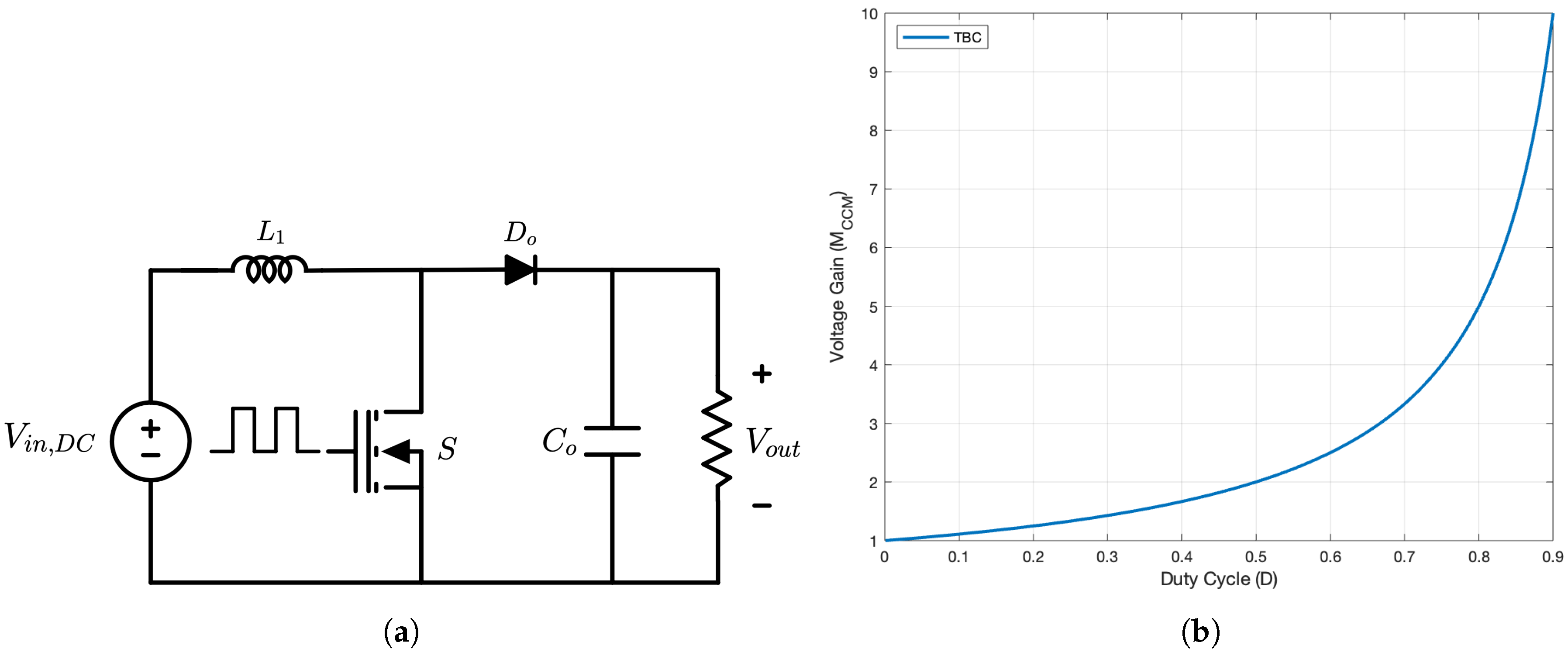
The TBC, which is shown in Figure 2, is the simplest and most fundamental topology of a non-isolated step-up DC–DC converter. That is because it has different advantages: the use of a single switch, the continuity of the source current, and the sharing of a common ground between the source and the load. However, in addition to these advantages, two main disadvantages make using TBCs undesirable: the low voltage gain with duty cycles lower than one and the high voltage stress between the main switch with respect to the output voltage. Operating TBCs or any other converter at a high duty cycle leads to an increase in current stress, resulting in increased conduction and switching losses and reduced efficiency [7]. Different techniques have been employed to overcome these issues in TBCs. One of these techniques is to insert a multistage switched inductor (SI) instead of the single inductor into the TBC to boost the voltage gain [8]. However, this multistage SI contains a large number of diodes and inductors, which will increase the number of elements in the circuit and, therefore, make it complex and inefficient. Another technique is to insert SI cells and switched capacitor (SC) cells into the TBC in a topology called a switched-inductor multilevel boost converter [9] to increase the voltage gain. However, the problem of requiring a large number of components reemerges, resulting in a larger complexity and inefficiency in the converter. Furthermore, in both techniques, the output voltage is low and fails to reach the desired high levels.
Different techniques are employed with non-isolated step-up DC–DC converters to increase their voltage gain, such as cascade [10,11], coupled inductor [12,13,14], quadratic [15,16], interleaved [17,18,19], or multilevel [20,21,22] converters. Cascaded converters can attain high voltage gain by merging various stages. However, they consist of a large number of circuit elements and have low efficiency. Similar to the isolated converters, coupled inductor converters can attain high voltage gains by selecting a specific value for the turn ratio. However, the overall efficiency of the converter is low due to leakage inductance, and the structure of the circuit design is complex due to the need for a snubber circuit to resolve the issue of leakage inductance. Moreover, quadratic converters can maintain high voltage gains; however, the circuit becomes complex due to the use of numerous elements, resulting in a reduction in efficiency. Although interleaved converters can attain high voltage gains, they utilize a large number of components, which is the main drawback of constructing such types of converters. Furthermore, multilevel converters also face the previously mentioned issue of having an increased number of components. The voltage gain of the multilevel converter that is presented in [23] depends on the number of voltage multipliers (VMs), mainly Cockcroft–Walton voltage multipliers that consist of several diodes and capacitors. As the number of VMs in the multilevel converters increases, the voltage gain will consequently increase. Ref. [24] presents several step-up and step-down voltage multiplier cells that can be integrated into different types of non-isolated DC–DC converters. In the proposed converters, an SI, which consists of two inductors, one capacitor, and two diodes, and an SC, which consists of two capacitors and two diodes, are utilized to design step-up converters that have high voltage gain while keeping the number of elements used at its minimum.
This paper is organized as follows: Section 2 describes the proposed SISC converter, including its two modes of operation and a comprehensive investigation of the derivation of the voltage gain and voltage stress equations. Similarly, Section 3 describes the proposed extended version of the SISC (ESISC) converter, including its two modes of operation and a comprehensive investigation of the derivation of the voltage gain and voltage stress equations. In Section 4, a comparison is made between the two proposed topologies and different early published converters in terms of the voltage gain, the voltage stress between the main switch, the switching frequency, and the total number of components. In Section 5, the simulation results are presented and discussed to determine whether they match the theoretical predictions. Finally, this paper concludes with a summary that highlights the key accomplishments made.

2. SISC Converter

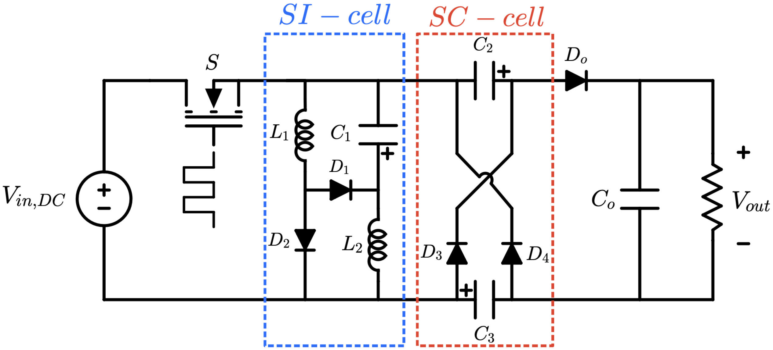
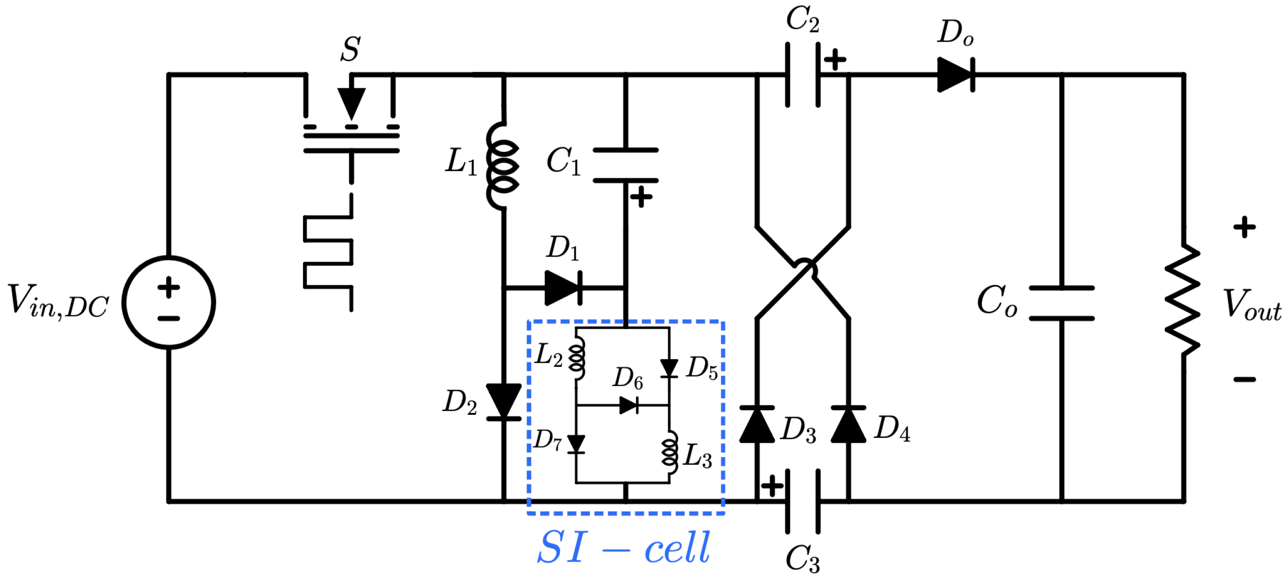
Figure 3 illustrates the proposed SISC converter, consisting of two VM cells: an SI and an SC. The SISC converter consists of two inductors ( L 1 and L 2 ), four capacitors ( C 1 , C 2 , C 3 , and C 0 ), five diodes ( D 1 , D 2 , D 3 , D 4 , and D 0 ), and a switch (S). As can be clearly seen from the structure of the circuit, the output voltage polarity is positive, guaranteeing compatibility with downstream elements.
To obtain the fundamental expressions of the proposed SISC and ESISC converters, the subsequent assumptions are posited:
  • All the circuit elements are lossless.
  • The inductors’ values are adequately high to guarantee working in continuous conduction mode (CCM).
  • The capacitors’ values are adequately high to provide constant voltage without any ripples during converter operation.
  • The two proposed topologies have two modes according to the operation of their semiconductor switches.
The equivalent circuit of the first mode of the proposed SISC converter is shown in Figure 4a. As shown in this figure, the switch (S) is ON and three diodes are reverse-biased, which are D 1 , D 3 , and D 4 . However, two diodes are forward-biased, which are D 2 and D 0 . During this mode, the first inductor ( L 1 ) is magnetized and charged by the input voltage ( V i n ).
V L 1 = V i n
Similarly, the second inductor ( L 2 ) is magnetized and charged by V i n with the discharged energy of the first capacitor ( C 1 ).
V L 2 = V i n + V C 1
The load is supplied by the discharged energy of the second and third capacitors ( C 2 and C 3 ) with V i n .
On the other hand, the equivalent circuit of the second mode of the proposed SISC converter is shown in Figure 4b. As shown in this figure, S is OFF and three diodes are forward-biased, which are D 1 , D 3 , and D 4 . However, two diodes are reverse-biased, which are D 2 and D 0 . During this mode, L 1 and L 2 are demagnetized due to the negative voltage on them, and they charge C 1 , C 2 , and C 3 . Hence, C 2 = C 3 .
V L 1 = V C 1
V L 2 = V C 1 V C 2
At the same time, the load is powered by the discharged energy of the output capacitor ( C 0 ). According to the voltage-second balance principle, the average voltage between L 1 and L 2 is zero; therefore, the following two equations are derived.
V i n D V C 1 ( 1 D ) = 0
( V i n + V C 1 ) D + ( V C 1 V C 2 ) ( 1 D ) = 0
By solving Equation (5), the voltage between C 1 is obtained.
V C 1 = D 1 D V i n
By solving Equation (6) and considering Equation (7), the voltage between C 2 , which is the same voltage between C 3 is obtained.
V C 2 = V C 3 = 2 D D 2 ( 1 D ) 2 V i n
Consequently, the proposed SISC converter’s voltage gain in CCM is obtained.
M C C M S I S C = V o u t V i n = I i n I o u t = 1 + 2 D D 2 ( 1 D ) 2
Now, the derived voltages between the capacitors and inductors are utilized to find the voltage stresses between the switches. Voltage stress refers to the amount of voltage present between either the main switch or the diode when they are turned OFF. During the first mode, D 1 , D 3 , and D 4 are OFF; therefore, the voltage stresses between them are calculated.
V D 1 = V i n 1 D = ( 1 D ) V o u t 1 + 2 D D 2
V D 3 = V D 4 = V i n ( 1 D ) 2 = V o u t 1 + 2 D D 2
Similarly, during the second mode, D 2 , D 0 , and S are OFF; therefore, the voltage stresses between them are calculated.
V D 2 = D V i n ( 1 D ) 2 = D V o u t 1 + 2 D D 2
V D 0 = V S = V i n ( 1 D ) 2 = V o u t 1 + 2 D D 2
The designs of the inductors’ values used in this converter with the help of V i n , V o u t , D, f S , and Δ i L , which is the inductor ripple, are computed using the following expressions:
L 1 = D V i n Δ i L 1 f S = D ( 1 D ) 2 V o u t ( 1 + 2 D D 2 ) Δ i L 1 f S
L 2 = D V i n ( 1 D ) Δ i L 2 f S = D ( 1 D ) 2 V o u t ( 1 D ) ( 1 + 2 D D 2 ) Δ i L 2 f S

3. Extended Topology of SISC Converter

Figure 5 clarifies the proposed extended SISC (ESISC) converter, which is composed of three inductors, three capacitors, eight diodes, and a switch. Similar to the proposed SISC converter, the extended one has a positive polarity at the output. The ESISC converter is obtained by replacing L 2 in the SISC converter with another SI, which involves two inductors ( L 2 and L 3 ) and three diodes ( D 5 , D 6 , D 7 ). Therefore, the ESISC converter has in total three inductors, four capacitors, eight diodes, and a single switch.
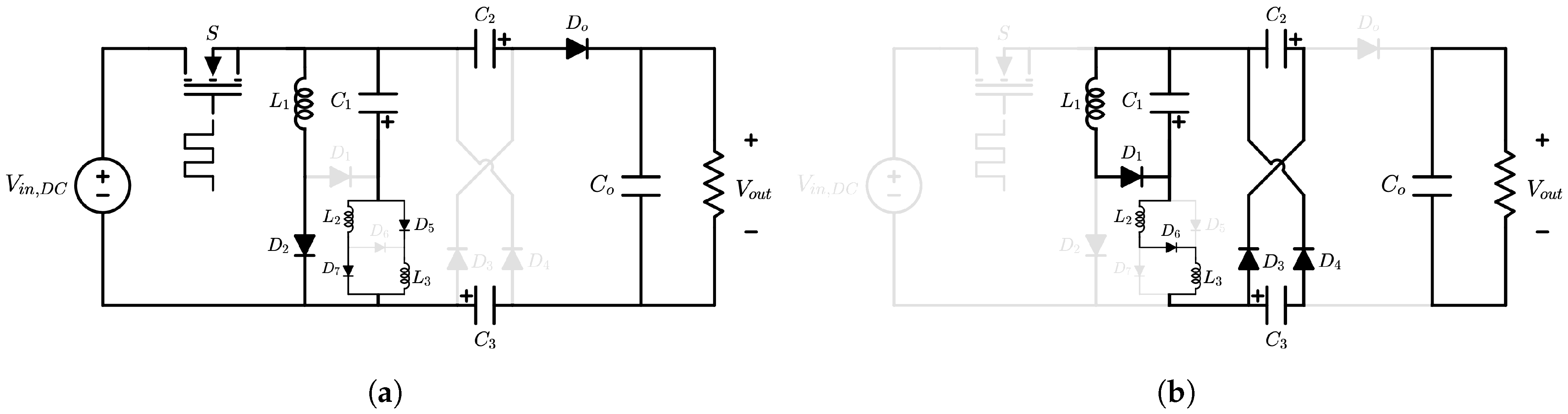
The equivalent circuit of the first mode of the proposed ESISC converter is shown in Figure 6a. As shown in this figure, S is ON and four diodes are reverse-biased, which are D 1 , D 3 , D 4 , and D 6 . However, four diodes are forward-biased, which are D 2 , D 5 , D 7 , and D 0 . During this mode, L 1 is magnetized and charged by V i n .
V L 1 = V i n
Similarly, L 2 and L 3 , which is the third inductor, are magnetized and charged by V i n with the discharged energy of C 1 . Hence, L 2 = L 3 .
V L 2 = V L 3 = V i n + V C 1
The load is supplied by the discharged energy of C 2 and C 3 with V i n .
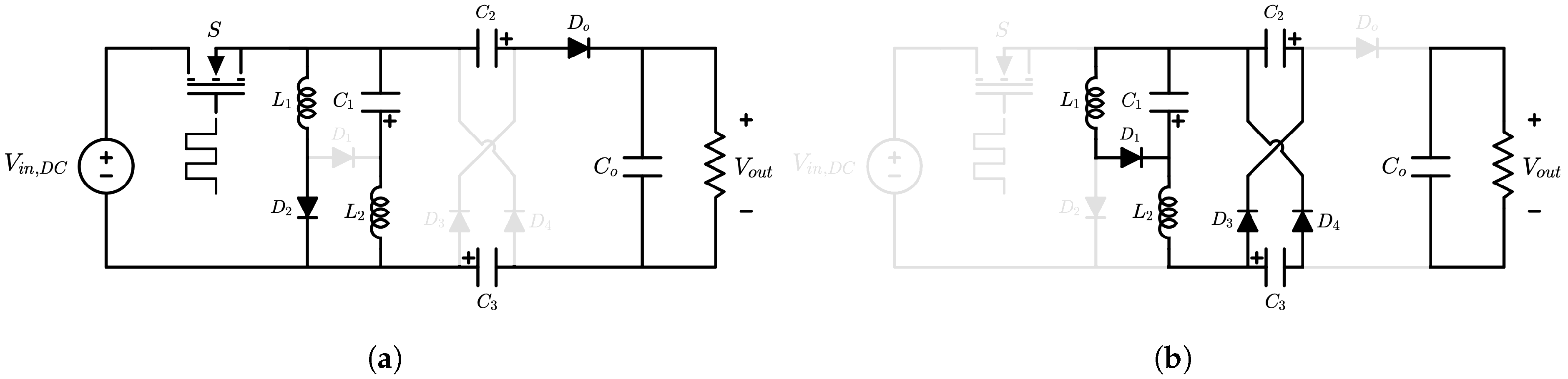
On the other hand, the equivalent circuit of the second mode of the proposed ESISC converter is shown in Figure 6b. As shown in this figure, S is OFF and four diodes are forward-biased, which are D 1 , D 3 , D 4 , and D 6 . However, four diodes are reverse-biased, which are D 2 , D 5 , D 7 , and D 0 . During this mode, L 1 , L 2 , and L 3 are demagnetized due to the negative voltage on them, and they charge C 1 , C 2 , and C 3 . Hence, C 2 = C 3 .
V L 1 = V C 1
V L 2 = V L 3 = V C 1 V C 2 2
At the same time, the load is powered by the discharged energy of the output capacitor ( C 0 ). According to the voltage-second balance principle, the average voltage between L 1 , L 2 , and L 3 is zero; therefore, the following two equations are derived.
V i n D V C 1 ( 1 D ) = 0
( V i n + V C 1 ) D + ( V C 1 V C 2 2 ) ( 1 D ) = 0
By solving Equation (20), the voltage between C 1 is obtained.
V C 1 = D 1 D V i n
By solving Equation (21) and considering Equation (22), the voltage between C 2 , which is the same voltage between C 3 is obtained.
V C 2 = V C 3 = 3 D D 2 ( 1 D ) 2 V i n
Consequently, the proposed ESISC converter’s voltage gain in CCM is obtained. Although only five elements are added to the extended one, the voltage gain of the extended converter is approximately twice that of the SISC converter when D = 75 % , as can be seen in Equation (24).
M C C M E S I S C = V o u t V i n = I i n I o u t = 1 + 4 D D 2 ( 1 D ) 2
Now, the derived voltages between the capacitors and inductors are utilized to find the voltage stresses between the switches. During the first mode, D 1 , D 3 , D 4 , and D 6 are OFF; therefore, the voltage stresses between them are calculated.
V D 1 = V D 6 = V i n 1 D = ( 1 D ) V o u t 1 + 4 D D 2
V D 3 = V D 4 = ( 1 + D ) V i n ( 1 D ) 2 = ( 1 + D ) V o u t 1 + 4 D D 2
Similarly, during the second mode, D 2 , D 5 , D 7 , D 0 , and S are OFF; therefore, the voltage stresses between them are calculated.
V D 2 = 2 D V i n ( 1 D ) 2 = 2 D V o u t 1 + 4 D D 2
V D 5 = V D 7 = D V i n ( 1 D ) 2 = D V o u t 1 + 4 D D 2
V D 0 = V S = ( 1 + D ) V i n ( 1 D ) 2 = ( 1 + D ) V o u t 1 + 4 D D 2
The designs of the inductors’ values used in this converter with the help of V i n , V o u t , D, f S , and Δ i L , which is the inductor ripple, are computed using the following expressions:
L 1 = D V i n Δ i L 1 f S = D ( 1 D ) 2 V o u t ( 1 + 4 D D 2 ) Δ i L 1 f S
L 2 = D V i n ( 1 D ) Δ i L 2 f S = D ( 1 D ) 2 V o u t ( 1 D ) ( 1 + 4 D D 2 ) Δ i L 2 f S

4. Comparison Analysis

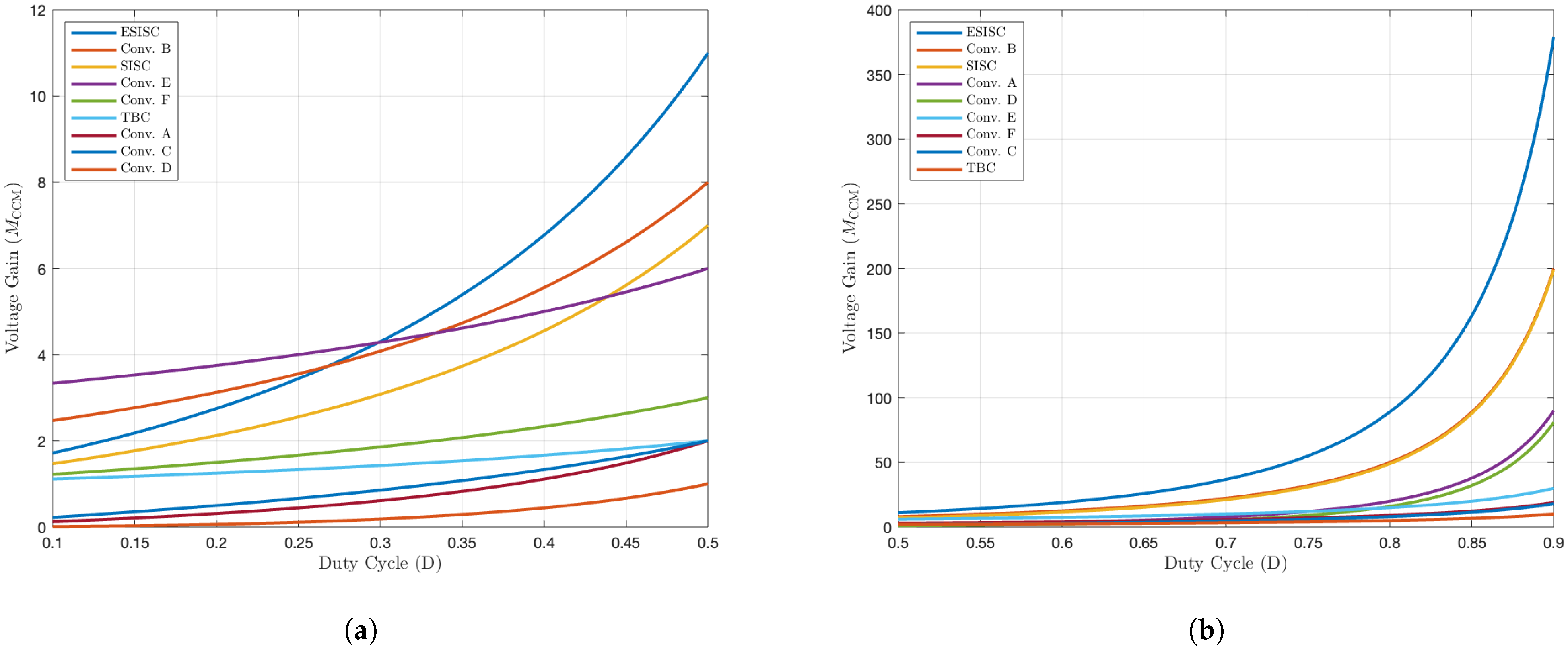
Table 1 summarizes a detailed comparison analysis of the proposed converters, SISC and ESISC, with the newly published non-isolated step-up DC–DC converters [25,26,27,28,29,30]. This comparison focuses on various criteria: the voltage gain in CCM, the voltage stress on the main switch, the switching frequency, the efficiency, the common ground availability, and the number of components. There are several factors to take into account when comparing step-up converters. The first factor is the voltage gain, which is considered the main aspect. Figure 7 shows a voltage gain comparison between the two proposed converters and other step-up converters as a function of the duty cycle. As this figure shows, the proposed converters have a higher voltage gain than all other suggested step-up converter topologies. The second factor is the voltage stress on the main switch S, ( V S / V o u t ) . When the duty cycle is higher than 50 % , the ( V S / V o u t ) will be around 50 % of the output voltage. However, when the duty cycle is less than 50 % , ( V S / V o u t ) is more than 50 % of the output voltage but never exceeds one. In contrast, the other boost topologies are being compared with experienced voltage stresses on their main switch that are equal to or greater than the output voltages of those topologies. The step-up converter in [26] has a higher voltage gain than the SISC converter, but it also experiences voltage stress on the main switch that is equal to its output voltage. Unfortunately, the efficiency of the proposed converters is not high enough but is acceptable compared to other converters.
From a component count and cost viewpoint, the proposed SISC and ESISC converters, as well as the compared converters, utilize a single active switch and avoid the use of transformers or coupled inductors. Therefore, the number of passive components and the voltage stress on the main active switch primarily influence the overall cost. Although the ESISC topology requires a larger number of passive electric elements to achieve a substantial high voltage gain, the voltage stress on the main switch is reduced to half of the output voltage, allowing the use of a lower-rated and lower-cost active switch. The proposed SISC converter, with a component count equal to [26,28], offers a reasonable cost tradeoff while attaining a higher voltage gain. The proposed converters, along with the topologies described in [25,30], are primarily designed for renewable energy applications, especially PVs, where a high step-up voltage gain is required. The converter presented in [26] is designed for high step-up DC systems requiring high voltage gain through quadratic and voltage multiplier techniques. The converter presented in [27] is designed for high-power, high-efficiency, and complex control applications, such as electric vehicle charging systems. The converter presented in [28] is designed for applications demanding a wide input voltage range with continuous input and output currents. Finally, Ref. [29] proposes a converter for DC microgrid applications, where high step-up capability and efficient power conversion are required. Additional information on these converters can be found in their relevant references.

5. Simulation Results

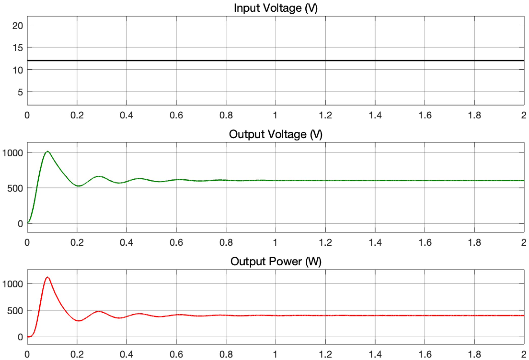
The two proposed converters (SISC and ESISC) are designed and analyzed using Matlab/Simulink software, which is a well-suited and trusted simulator. Before starting to analyze the two converters, different values have to be set up, such as input voltage, output voltage, output power, switching frequency, duty cycle, capacitor values, and inductor values. All of these necessary values are provided in Table 2.

5.1. SISC Converter

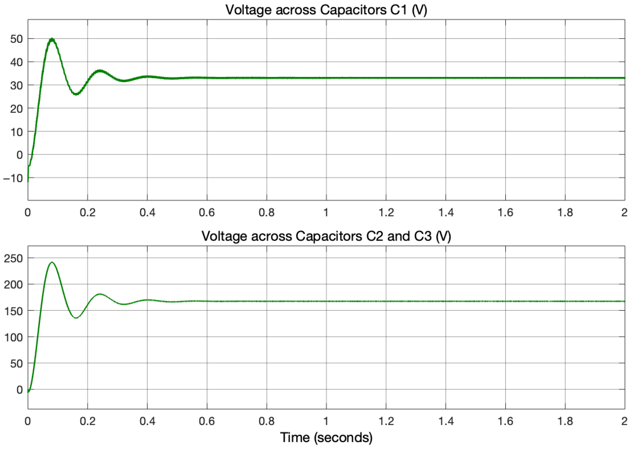
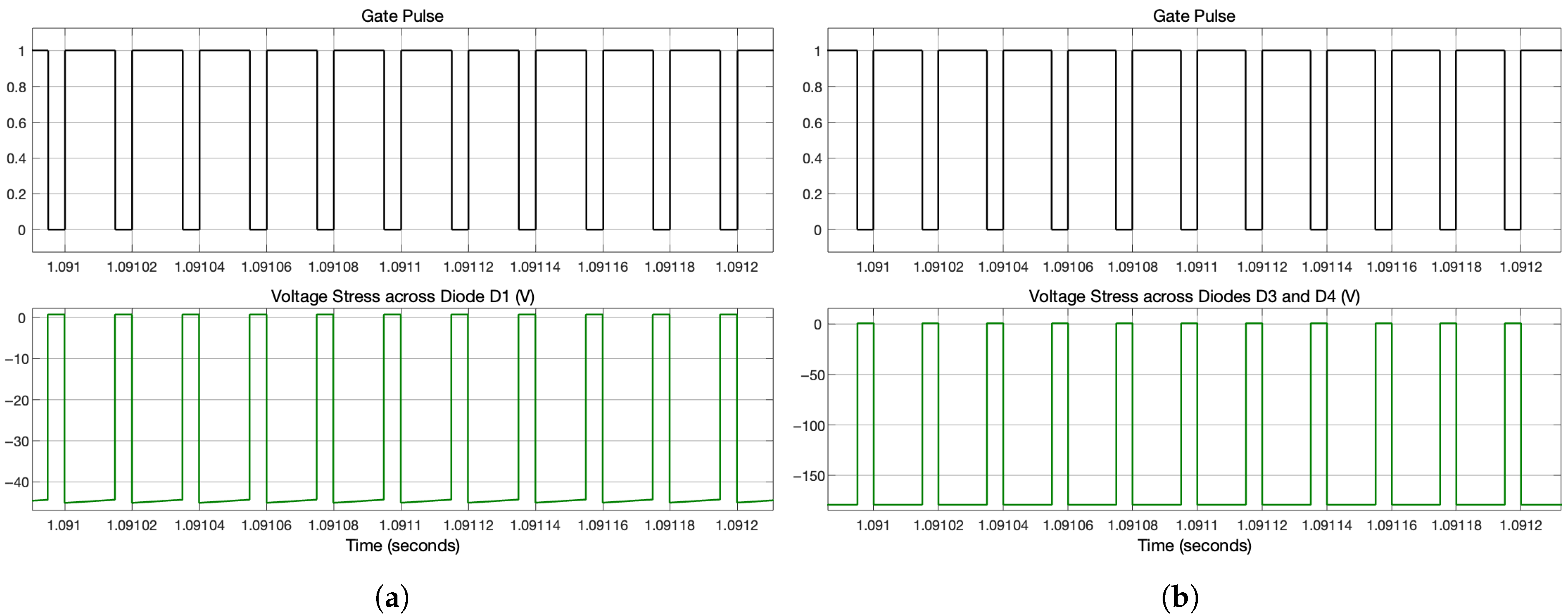
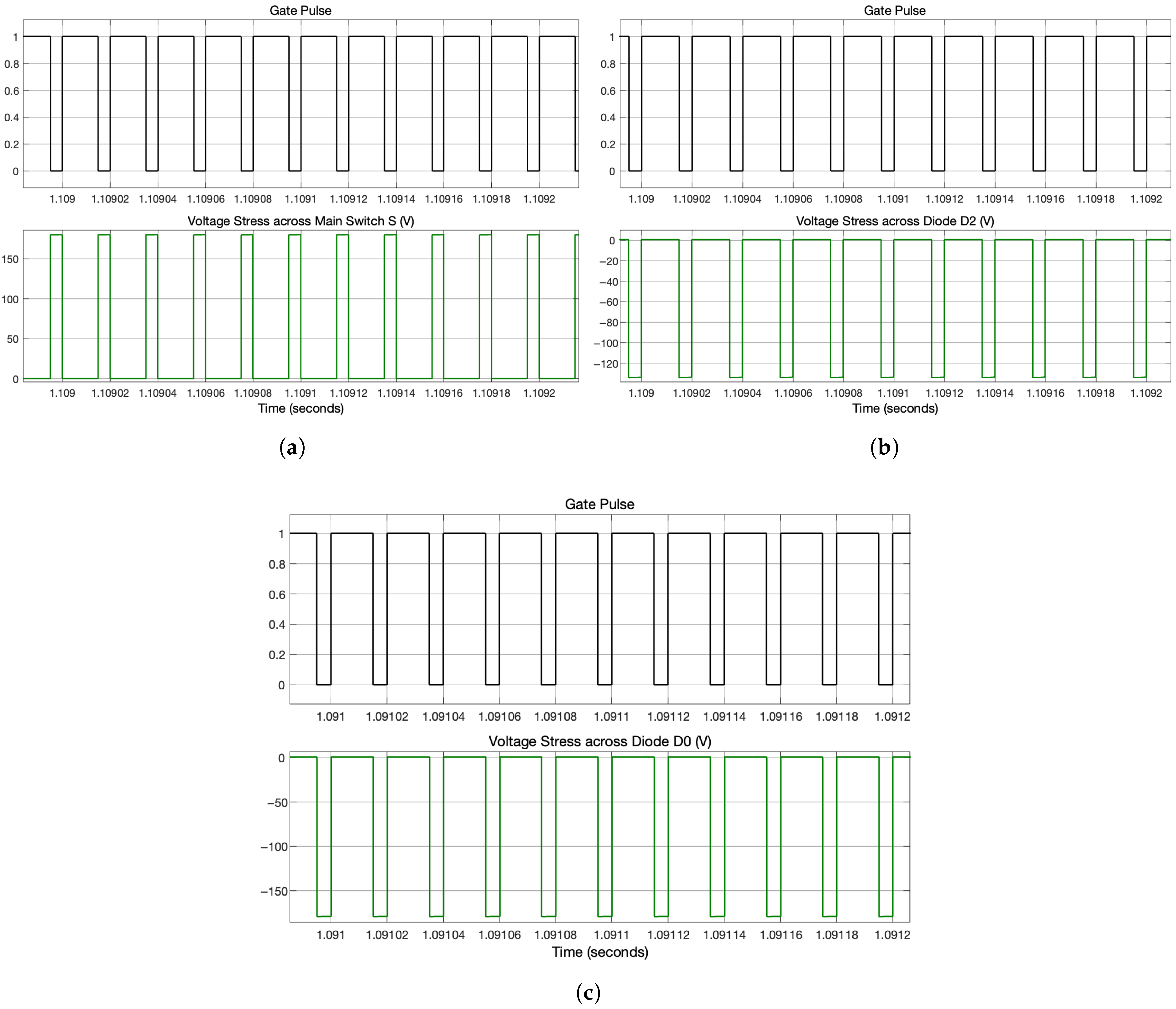
A 400 W, 345 V model is simulated and tested to validate the performance of the proposed SISC converter under steady-state operation conditions. The main purpose is to justify the exact functionality of the proposed converter in terms of the voltage gain and the voltage stress between active and passive switches. The input voltage of 12 V is increased to an output voltage of 345 V with a duty cycle of 0.75 and an output power of 400 W, as shown in Figure 8. The voltage waveforms between the capacitors C 1 , C 2 , and C 3 are shown in Figure 9. Equations (7) and (8) predict the voltages of C 1 and C 2 , which is the exact same voltage between C 3 , are 36 V and 180 V, respectively. The voltage stresses between the diodes D 1 , D 2 , D 3 , D 4 , and D 0 , and the main switch S when off are shown in Figure 10 and Figure 11. As can be calculated from Equations (10)–(13), the voltage stresses between the switches are V D 1 = 45 V, V D 3 = V D 4 = 178 V, V D 2 = 134 V, and V D 0 = V S = 178 V. The figures of the simulated waveforms, the derived equations, and the results clearly show their convergence.

5.2. ESISC Converter

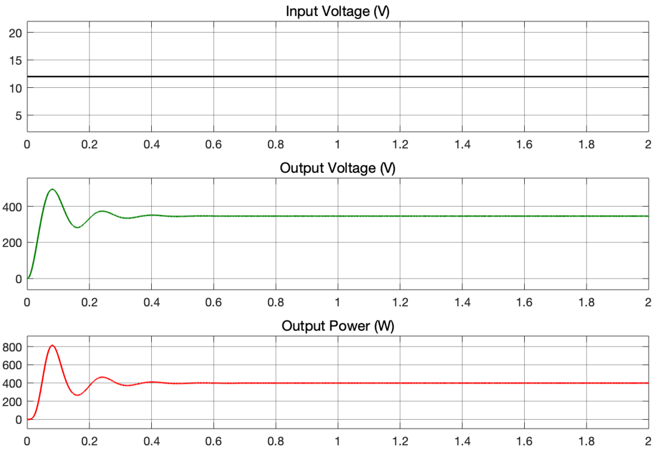
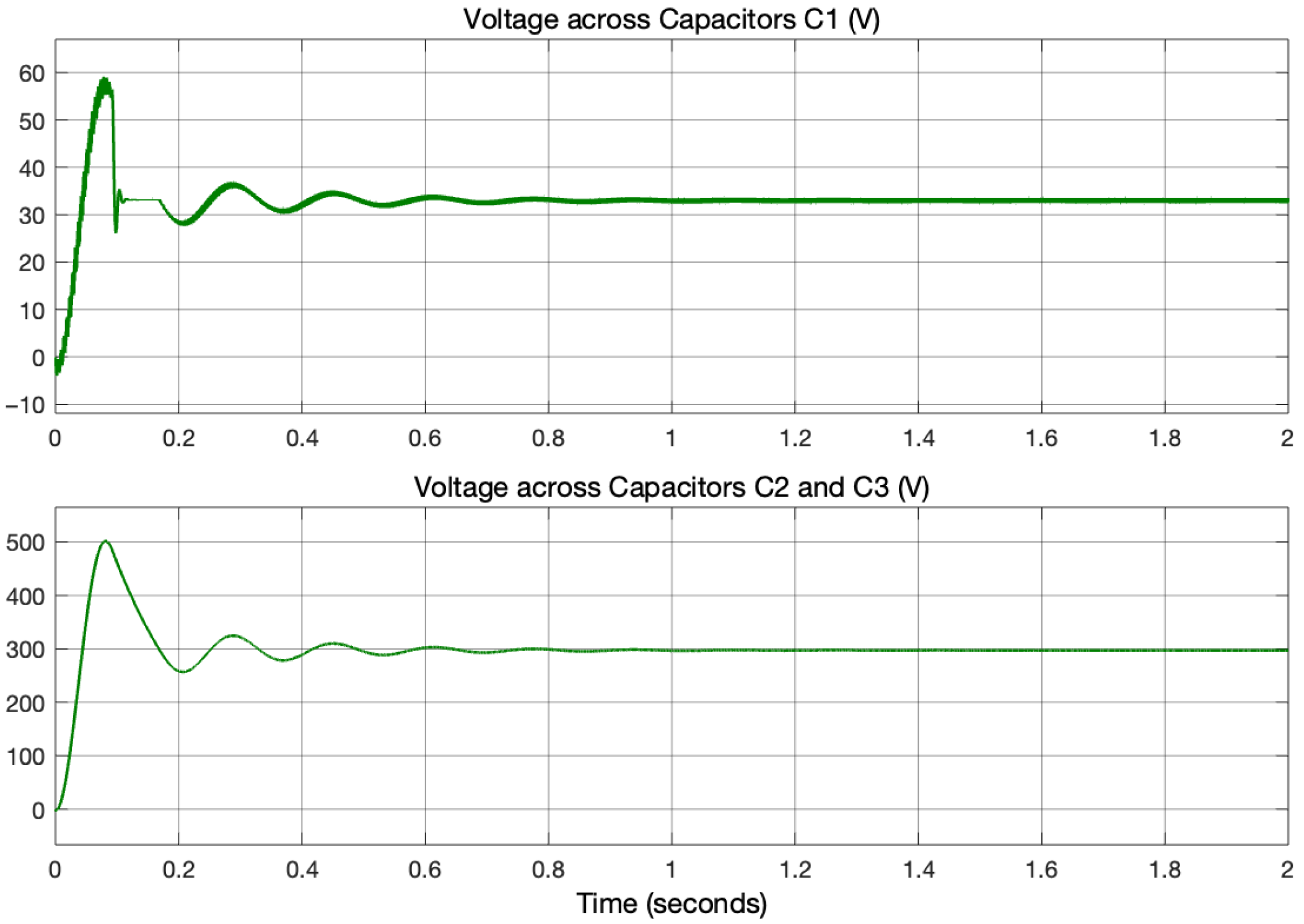
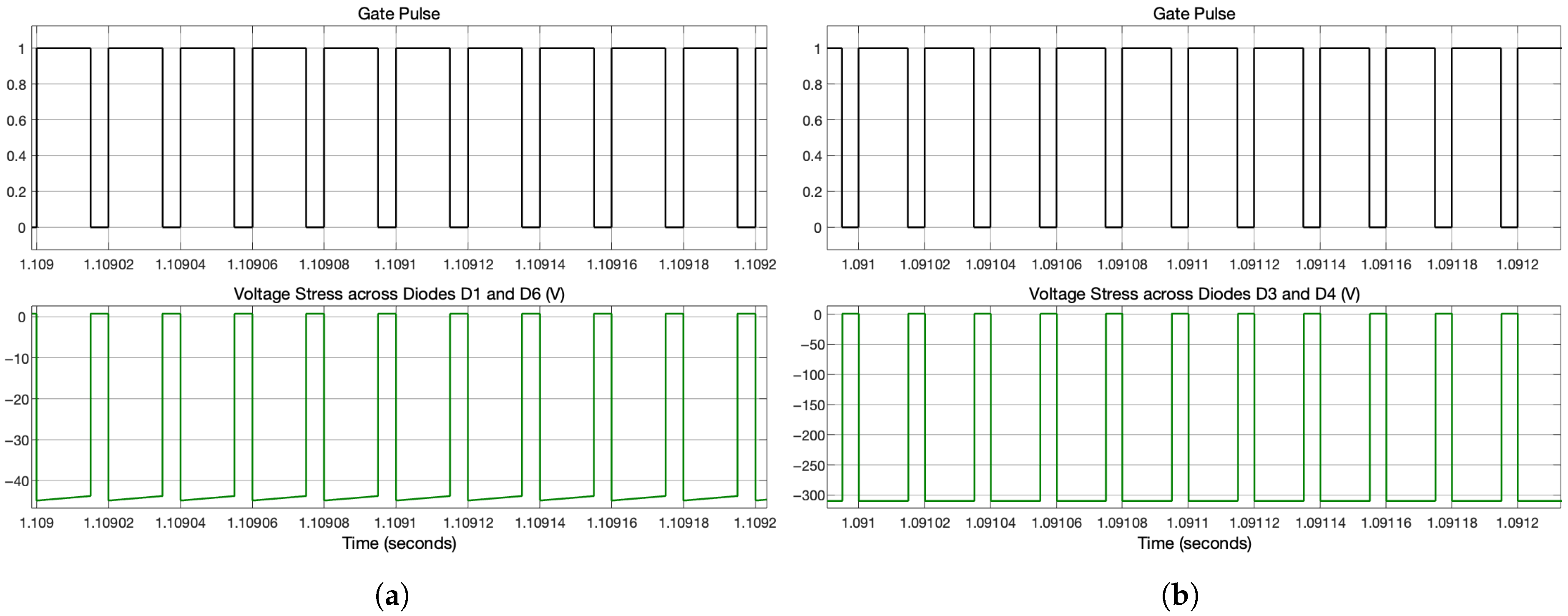
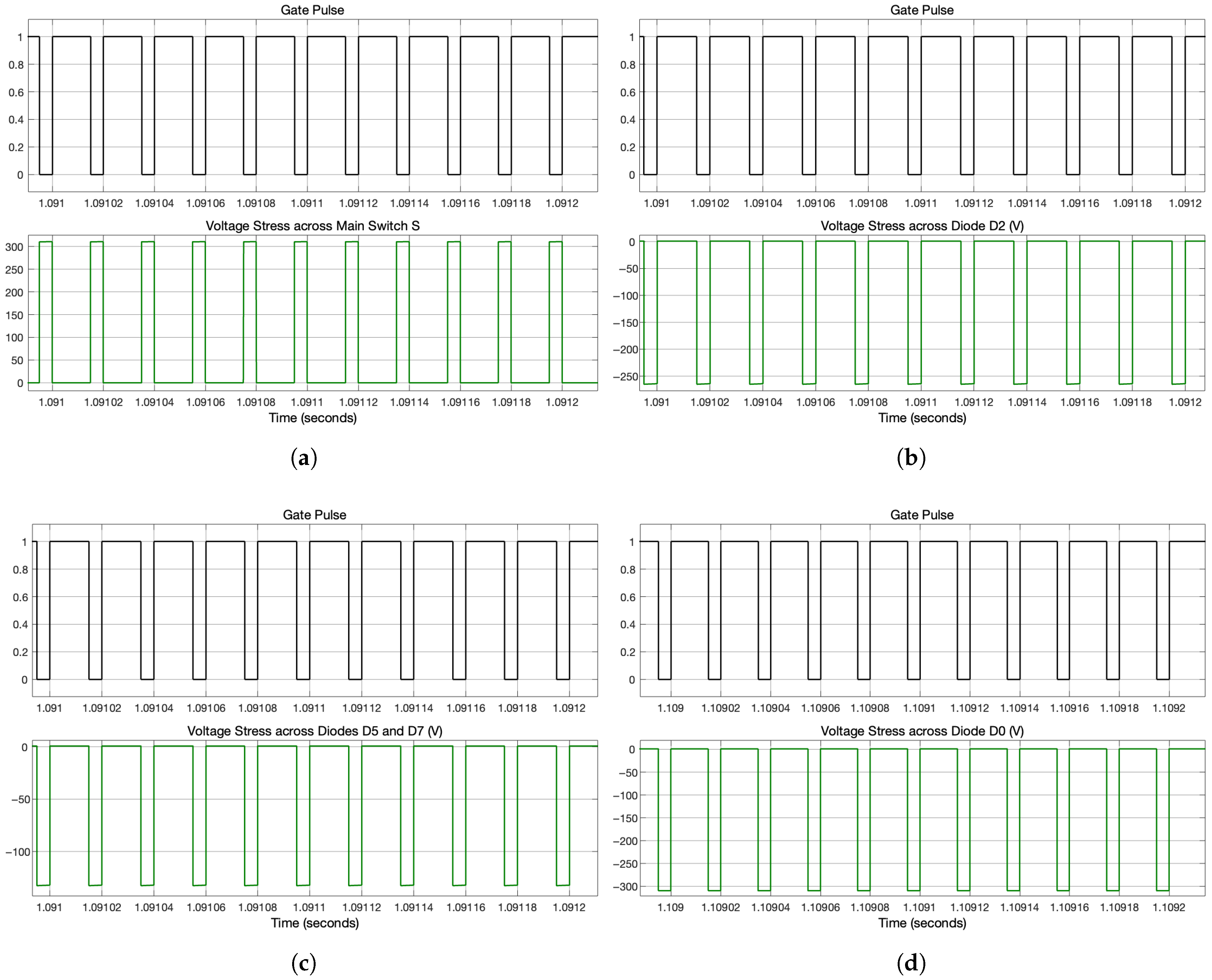
A 400 W, 605 V model is simulated and tested to validate the performance of the proposed ESISC converter under steady-state operation conditions. The main purpose is to justify the exact functionality of the proposed converter in terms of the voltage gain and the voltage stress between active and passive switches. The input voltage of 12 V is increased to an output voltage of 605 V with a duty cycle of 0.75 and an output power of 400 W, as shown in Figure 12. The voltage waveforms between the capacitors C 1 , C 2 , and C 3 are shown in Figure 13. Equations (20) and (21) predict the voltages of C 1 and C 2 , which is the exact same voltage between C 3 , 36 V and 324 V, respectively. The voltage stresses between the diodes D 1 , D 2 , D 3 , D 4 , D 5 , D 6 , D 7 , and D 0 , and the main switch S when off are shown in Figure 14 and Figure 15. As can be calculated from Equations (23)–(27), the voltage stresses between the switches are V D 1 = V D 6 = 44 V, V D 2 = 264 V, V D 3 = V D 4 = 308 V, V D 5 = V D 7 = 132 V, and V D 0 = V S = 308 V. The figures of the simulated waveforms, the derived equations, and the results clearly show their convergence.
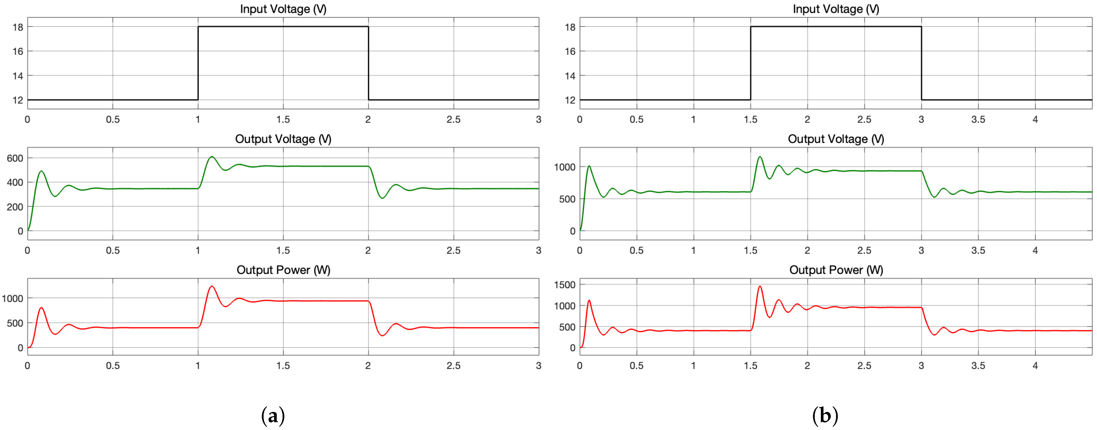
The stability of the two proposed converters is tested by introducing a disturbance to the input voltage and observing whether the output voltage will converge. A disturbance is applied by changing the input voltage from 12 V to 18 V, which represents an increase of 50 % , and then returning to 12 V, as can be seen in Figure 16. The observed transient overshoot is attributed to a sudden input voltage change and the absence of a closed-loop controller. The proposed converters remain stable, and all state variables converge to steady-state values.

6. Conclusions

This article has successfully discussed developing two topologies, SISC and ESISC, of step-up converters with high voltage gains. The method utilized to increase the input voltage involves the integration of an SI cell and an SC cell within the DC–DC converter. This substantial high voltage gain, which is approximately sixty times the input voltage when the duty cycle is 0.75 in the ESISC converter, is achieved without the use of a transformer, a very high duty cycle value, or coupled inductors. A comparison is made between the proposed topologies and different types of step-up DC–DC converters, showing that the proposed topologies are among the highest voltage gains. The proposed converters offer several advantages: high voltage gain; use of a single active switch; lower voltage stress on the main active switch with respect to the output voltage; and relatively few components, especially in the SISC converter. The voltage gain equations in steady-state are fully derived in detail, which agrees with the simulation results obtained by Matlab/Simulink software.

Funding

This research received no external funding.

Data Availability Statement

The original contributions presented in this study are included in the article. Further inquiries can be directed to the corresponding author.

Conflicts of Interest

The author declares no conflicts of interest.

References

  1. Gupta, T.; Pandit, G.K.; Sharan, B.; Mishra, H.; Singh, S.; Dewan, R. A robust approach for analysis and visualization of CO2 and greenhouse gas emission and its effect. In Proceedings of the 10th International Conference on Computing for Sustainable Global Development (INDIACom), New Delhi, India, 15–17 March 2023; IEEE: New York, NY, USA, 2023; pp. 238–243. [Google Scholar]
  2. Atia, R.; Yamada, N. Sizing and analysis of renewable energy and battery systems in residential microgrids. IEEE Trans. Smart Grid 2016, 7, 1204–1213. [Google Scholar] [CrossRef] [Scilit]
  3. Patterson, M.; Macia, N.F.; Kannan, A.M. Hybrid microgrid model based on solar photovoltaic battery fuel cell system for intermittent load applications. IEEE Trans. Energy Convers. 2015, 30, 359–366. [Google Scholar] [CrossRef] [Scilit]
  4. Kheirollahi, R.; Zhao, S.; Zhang, H.; Lu, X.; Wang, J.; Lu, F. Coordination of ultrafast solid-state circuit breakers in radial DC microgrids. IEEE Trans. Emerg. Sel. Top. Power Electron. 2022, 10, 4690–4702. [Google Scholar] [CrossRef] [Scilit]
  5. Zhu, X.; Zhang, B.; Li, Z.; Li, H.; Ran, L. Extended switched-boost DC-DC converter adopting switched-capacitor/switched-inductor cells for high step-up conversion. IEEE J. Emerg. Sel. Top. Power Electron. 2017, 5, 1020–1030. [Google Scholar] [CrossRef] [Scilit]
  6. Gong, L.; Peng, Y.; Cui, C.; Chen, J.; Jiang, L.; Xu, J.; Fang, X.; Wang, Y. A hybrid phase-frequency control of dual active bridge converters for hold-up time extension in more electric aircrafts applications. IEEE Trans. Power Electron. 2024, 39, 14135–14141. [Google Scholar] [CrossRef] [Scilit]
  7. Hasanpour, S.; Siwakoti, Y.; Blaabjerg, F. A new soft-switching high gain DC/DC converter with bipolar outputs. IET Power Electron. 2024, 17, 144–156. [Google Scholar] [CrossRef] [Scilit]
  8. Maroti, P.; Padmanaban, S.; Bhaskar, M.; Blaabjerg, F.; Ramachandaramurthy, V.; Siano, P.; Fedák, V. Multistage switched inductor boost converter for renewable energy application. In Proceedings of the IEEE Conference on Energy Conversion (CENCON), Kuala Lumpur, Malaysia, 30–31 October 2017; IEEE: New York, NY, USA, 2017. [Google Scholar] [CrossRef] [Scilit]
  9. Mousa, M.; Ahmed, M.; Orabi, M. A switched inductor multilevel boost converter. In Proceedings of the IEEE International Conference on Power and Energy, Kuala Lumpur, Malaysia, 29 November–1 December 2010; IEEE: New York, NY, USA, 2010. [Google Scholar] [CrossRef] [Scilit]
  10. Vinnikov, D.; Roasto, I.; Strzelecki, R.; Adamowicz, M. Step-up DC/DC converters with cascade quasi-Z-source network. IEEE Trans. Ind. Electron. 2012, 59, 3727–3736. [Google Scholar] [CrossRef] [Scilit]
  11. Lopez, M.; Ramos, J.; Gutierrez, E.; Saldana, J. Modeling and analysis of switch-mode cascade converters with a single active switch. IET Power Electron. 2008, 1, 478–487. [Google Scholar] [CrossRef] [Scilit]
  12. Forouzesh, M.; Shen, Y.; Yari, K.; Siwakoti, Y.P.; Blaabjerg, F. High-efficiency high step-up DC-DC converter with dual coupled inductors for grid-connected photovoltaic systems. IEEE Trans. Power Electron. 2018, 33, 5976–5982. [Google Scholar] [CrossRef] [Scilit]
  13. Samadian, A.; Hosseini, S.H.; Sabahi, M. A new three-winding coupled inductor nonisolated quasi-Z-source high step-up DC-DC converter. IEEE Trans. Power Electron. 2021, 36, 11523–11531. [Google Scholar] [CrossRef] [Scilit]
  14. Oh, Y.; Choi, W.; Kwon, J. Design of a step-up DC-DC converter for standalone photovoltaic systems with battery energy storages. Energies 2022, 15, 44. [Google Scholar] [CrossRef] [Scilit]
  15. Dizangian, N.; Jovanovic, S.; Poure, P. Modeling and experimental verification of a single-switch quadratic boost DC-DC converter with high voltage gain for energy harvesting. Energies 2025, 18, 5447. [Google Scholar] [CrossRef] [Scilit]
  16. Babaiahgari, B.; Valdez-Resendiaz, J.E.; Alejo-Reyes, A.; Rosas-Caro, J.C.; Silva-Vera, E.D. Quadratic boost converter with reduced current ripple. Appl. Sci. 2025, 15, 10815. [Google Scholar] [CrossRef] [Scilit]
  17. Algamluoli, A.; Wu, X. Ultra-high voltage gain DC-DC converter based on new interleaved switched capacitor inductor for renewable energy systems. Int. J. Circuit Theory Appl. 2023, 52, 2435–2465. [Google Scholar] [CrossRef] [Scilit]
  18. Allehyani, A. An interleaved multilevel DC-DC boost converter with direct input to output connection. IEEE Trans. Ind. Appl. 2023, 59, 7027–7038. [Google Scholar] [CrossRef] [Scilit]
  19. Samuel, V.L.; Keerthi, G.; Prabhakar, M. Ultra-high gain DC-DC converter based on interleaved quadratic boost converter with ripple-free input current. Int. Trans. Electr. Energy Syst. 2020, 30, e12622. [Google Scholar] [CrossRef] [Scilit]
  20. Khalid, H.; Mekheilef, S.; Siddique, M.; Mubin, M.; Seyedmahmoudian, M.; Stojcevski, A.; Ahmed, M. A high voltage gain multi-stage DC-DC boost converter with reduced voltage stress. IETE J. Res. 2022, 70, 2032–2046. [Google Scholar] [CrossRef] [Scilit]
  21. Shoaei, A.; Abbaszadeh, K.; Allahyari, H. A single-inductor multi-input multi-level high step-up DC-DC converter based on switched-diode-capacitor cells for PV applications. IEEE J. Emerg. Sel. Top. Ind. Electron. 2023, 4, 18–27. [Google Scholar] [CrossRef] [Scilit]
  22. Ranjana, M.; SreeramulaReddy, N.; Kumar, R. A novel non-isolated switched inductor floating output DC-DC multilevel boost converter for fuelcell applications. In Proceedings of the IEEE Students’ Conference on Electrical, Electronics, and Computer Science (SCEECS), Bhopal, India, 1–2 March 2014; IEEE: New York, NY, USA, 2014; pp. 1–5. [Google Scholar] [CrossRef] [Scilit]
  23. Rajaei, A.; Khazan, R.; Mahmoudian, M.; Mardaneh, M.; Gitizadeh, M. A dual inductor high step-up DC/DC converter based on the cockcroft-walton multiplier. IEEE Trans. Power Electron. 2018, 33, 9699–9709. [Google Scholar] [CrossRef] [Scilit]
  24. Axelord, B.; Berkovich, Y.; Ioinovici, A. Switched-capacitor/switched-inductor structures for getting transformerless hybrid DC-DC PWM converters. IEEE Trans. Circuits Syst. I Regul. Pap. 2008, 55, 687–696. [Google Scholar] [CrossRef] [Scilit]
  25. Maroti, P.; Padmanaban, S.; Holm-Nielsen, J.; Bhaskar, M.; Meraj, M.; Iqbal, A. A new structure of high voltage gain SEPIC converter for renewable energy applications. IEEE Access 2019, 7, 89857–89868. [Google Scholar] [CrossRef] [Scilit]
  26. Rezaie, M.; Abbasi, V. Effective combination of quadratic boost converter with voltage multiplier cell to increase voltage gain. IET Power Electron. 2020, 13, 2322–2333. [Google Scholar] [CrossRef] [Scilit]
  27. Chandrasekar, G.; Lakshmanan, S. A high efficiency active X2G boost converter with hybrid optimized prportional integral controller for PV powered EV charging applications. Sci. Rep. 2025, 15, 36282. [Google Scholar] [CrossRef] [Scilit] [PubMed]
  28. Zhang, N.; Zhang, G.; See, K.; Zhang, B. A single-switch quadratic buck-boost converter with continuous input port current and continuous output port current. IEEE Trans. Power Electron. 2017, 33, 4157–4166. [Google Scholar] [CrossRef] [Scilit]
  29. Rafiee, R.; Batmani, Y. On the design of novel single-switch low loss boost converters with high step-up voltages. IEEE Trans. Power Electron. 2025, 40, 8206–8215. [Google Scholar] [CrossRef] [Scilit]
  30. Qin, L.; Zhou, L.; Hassan, W.; Soon, J.; Tian, M.; Shen, J. A family of transformer-less single-switch dual-inductor high voltage gain boost converters with reduced voltage and current stresses. IEEE Trans. Power Electron. 2021, 36, 5674–5685. [Google Scholar] [CrossRef] [Scilit]
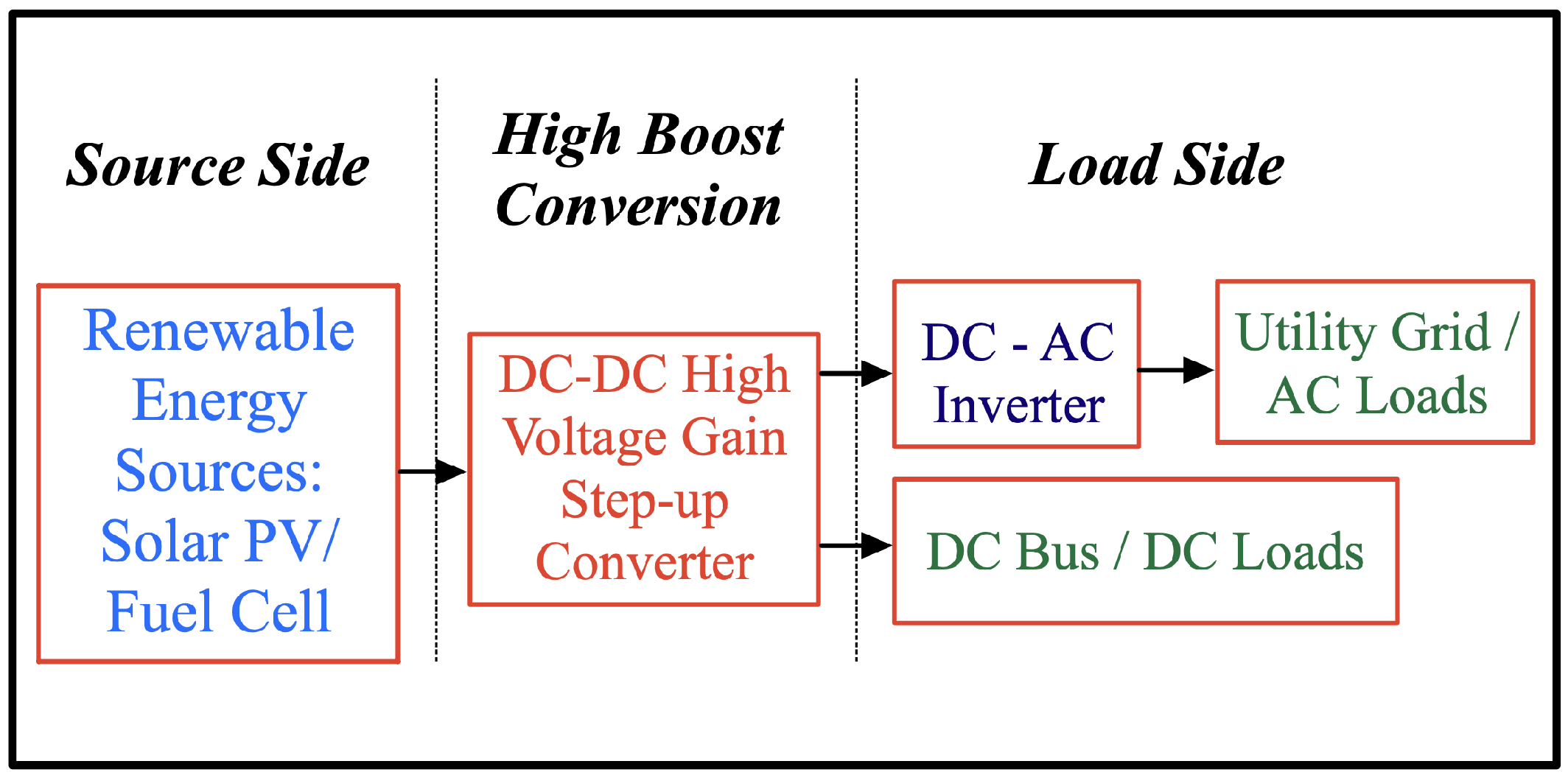
Figure 1. Block diagram of a renewable energy system utilizing a high-voltage-gain DC–DC converter.
Processes 14 00640 g001
Figure 2. Traditional boost converter (TBC): (a) layout; (b) voltage gain vs. duty cycle.
Processes 14 00640 g002
Figure 3. Main circuit of the SISC converter.
Processes 14 00640 g003
Figure 4. SISC converter: (a) Mode 1; (b) Mode 2.
Processes 14 00640 g004
Figure 5. Basic circuit of the ESISC converter.
Processes 14 00640 g005
Figure 6. ESISC converter: (a) Mode 1; (b) Mode 2.
Processes 14 00640 g006
Figure 7. Voltage gain comparison as a function of duty cycle: (a) between 0 % and 50 % duty cycle; (b) between 50 % and 90 % duty cycle. Conv. A, Conv. B, and Conv. C, Conv. D, Conv. E, and Conv. F correspond to the converters presented in [25,26,27,28,29], and [30] respectively.
Processes 14 00640 g007
Figure 8. V i n , V o u t , and P o u t waveforms of the SISC converter.
Processes 14 00640 g008
Figure 9. C 1 , C 2 , and C 3 waveforms of the SISC converter.
Processes 14 00640 g009
Figure 10. Voltage stresses of the SISC converter in the ON-mode: (a) voltage stress between D 1 ; (b) Voltage stresses between D 3 and D 4 .
Processes 14 00640 g010
Figure 11. Voltage stresses of the SISC converter in the OFF-mode: (a) voltage stress between S; (b) voltage stress between D 2 ; (c) voltage stress between D 0 .
Processes 14 00640 g011
Figure 12. V i n , V o u t , and P o u t waveforms of the ESISC converter.
Processes 14 00640 g012
Figure 13. C 1 , C 2 , and C 3 waveforms of the ESISC converter.
Processes 14 00640 g013
Figure 14. Voltage stresses of the ESISC converter in the ON-mode: (a) voltage stress between D 1 and D 6 ; (b) voltage stresses between D 3 and D 4 .
Processes 14 00640 g014
Figure 15. Voltage stresses of the ESISC converter in the OFF-mode: (a) voltage stress between S; (b) voltage stress between D 2 ; (c) voltage stresses between D 5 and D 7 ; (d) voltage stress between D 0 .
Processes 14 00640 g015
Figure 16. Time-domain response of the two proposed converters under an input voltage disturbance: (a) SISC converter. (b) ESISC converter.
Processes 14 00640 g016
Table 1. Comparison of the proposed converters with related boost converters in term of voltage gain, voltage stress on the main switch, switching frequency, and number of components.
T M CCM M CCM at D = 75 % V S V out V S at D = 75 % f S η CGS/D/L/C/T
TBC 1 1 D 41 V o u t --1/1/1/1/4
[25] D ( 1 D ) 2 121 V o u t 50 kHz 91.4 % 1/3/3/3/10
[26] 2 ( 1 D ) 2 321 V o u t 100 kHz 90 % 1/5/3/3/12
[27] 2 D 1 D 61 V o u t 10 kHz 96 % 1/6/2/4/13
[28] D 2 ( 1 D ) 2 9 1 D 2 2 V o u t 40 kHz 85 % 1/5/3/3/12
[29] 3 1 D 121 V o u t 50 kHz 95.1 % 1/8/3/3/15
[30] 1 + D 1 D 7 1 1 D 4 V o u t 100 kHz 97.4 % 1/8/3/3/15
SISC 1 + 2 D D 2 ( 1 D ) 2 31 1 1 + 2 D D 2 V o u t 2 50 kHz 84.2 % 1/5/2/4/12
ESISC 1 + 4 D D 2 ( 1 D ) 2 55 ( 1 + D ) 1 + 4 D D 2 V o u t 2 50 kHz 77.4 % 1/8/3/4/16
Note: M C C M = voltage gain in CCM, V S V o u t = normalized voltage stress on main switch, V S = voltage stress on main switch, f S = switching frequency, η = efficiency, CG = common ground, = has common ground, S = no. of switches, D = no. of diodes, L = no. of inductors, C = no. of capacitors, T = total no. of components.
Table 2. Parameters of the Matlab/Simulink simulator.
ParameterValue
Input voltage ( V i n )12 V
Output voltages ( V o u t )345 V/605 V
Rated power ( P o u t )400 W
Switching frequency ( f s )50 kHz
Duty cycle (D)75%
Inductor ( L 1 )1 mH
Inductors ( L 2 and L 3 )5 mH
Capacitor ( C 1 )200 μ F
Capacitors ( C 2 and C 3 )150  μ F
Capacitor ( C 0 )100 μ F
Disclaimer/Publisher’s Note: The statements, opinions and data contained in all publications are solely those of the individual author(s) and contributor(s) and not of MDPI and/or the editor(s). MDPI and/or the editor(s) disclaim responsibility for any injury to people or property resulting from any ideas, methods, instructions or products referred to in the content.