Article

Multimodal Switching Control Strategy for Wide Voltage Range Operation of Three-Phase Dual Active Bridge Converters

1
College of Electrical and Control Engineering, Liaoning Technical University, Huludao 125105, China
2
College of Information Science and Engineering, Northeastern University, Shenyang 110819, China
3
State Grid Jibei Electric Power Co., Ltd., Tangshan Power Supply Company, Tangshan 063099, China
*
Author to whom correspondence should be addressed.
Processes 2025, 13(6), 1921; https://doi.org/10.3390/pr13061921
Submission received: 15 May 2025 / Revised: 9 June 2025 / Accepted: 11 June 2025 / Published: 17 June 2025

Abstract

:
In recent years, to achieve “dual carbon” goals, increasing the penetration of renewable energy has become a critical approach in China’s power sector. Power electronic converters play a key role in integrating renewable energy into the power system. Among them, the Dual Active Bridge (DAB) DC-DC converter has gained widespread attention due to its merits, such as galvanic isolation, bidirectional power transfer, and soft switching. It has been extensively applied in microgrids, distributed generation, and electric vehicles. However, with the large-scale integration of stochastic renewable sources and uncertain loads into the grid, DAB converters are required to operate over a wider voltage regulation range and under more complex operating conditions. Conventional control strategies often fail to meet these demands due to their limited soft-switching range, restricted optimization capability, and slow dynamic response. To address these issues, this paper proposes a multi-mode switching optimized control strategy for the three-port DAB (3p-DAB) converter. The proposed method aims to broaden the soft-switching range and optimize the operation space, enabling high-power transfer capability while reducing switching and conduction losses. First, to address the issue of the narrow soft-switching range at medium and low power levels, a single-cycle interleaved phase-shift control mode is proposed. Under this control, the three-phase Dual Active Bridge can achieve zero-voltage switching and optimize the minimum current stress, thereby improving the operating efficiency of the converter. Then, in the face of the actual demand for wide voltage regulation of the converter, a standardized global unified minimum current stress optimization scheme based on the virtual phase-shift ratio is proposed. This scheme establishes a unified control structure and a standardized control table, reducing the complexity of the control structure design and the gain expression. Finally, both simulation and experimental results validate the effectiveness and superiority of the proposed multi-mode optimized control strategy.

1. Introduction

In recent years, the global energy crisis has accelerated the search for clean and efficient alternatives to fossil fuels [1]. With the goal of achieving carbon neutrality and peak carbon emissions, countries worldwide are promoting the transition to low-carbon energy systems [2]. China, in particular, has proposed the “dual carbon” target, which places increasing pressure on the power industry to integrate more renewable energy sources [3]. However, the shift towards renewable energy introduces challenges due to the intermittency and randomness of sources like wind and solar [4]. These challenges are especially significant for grid stability and efficient energy conversion [5], particularly in hybrid wind/solar systems where accurate current sharing and voltage regulation are critical [6]. As the International Energy Agency warns of continued pressure on global electricity demand, innovations in power electronic converters become essential [7].
The Dual Active Bridge (DAB) DC converter is often used in the energy exchange field due to its advantages such as electrical isolation, bidirectional energy flow, and easy realization of soft switching [8,9]. In practical applications, the three-phase DAB (3p-DAB) converter has become a key component in many energy systems, which typically require high power density and flexible voltage adaptation capabilities. For example, in the vehicle-to-vehicle energy sharing system [10], as an intermediate energy converter, DAB realizes fast bidirectional energy transmission between electric vehicles and needs to maintain soft-switching performance within a wide voltage range. Similarly, in microgrid and distributed generation systems [11,12], 3p-DAB is often used to connect distributed energy sources with DC buses, achieving efficient energy routing and enhanced system stability. In these scenarios, the operating conditions are complex and changeable, and frequent mode switching and voltage fluctuations place higher demands on control strategies. Therefore, the control method not only needs to optimize converters with specific rated power but also have good scalability and adaptability [13]. Although the multi-mode switching strategy proposed in this paper is verified based on a 15 kW prototype, it is essentially driven by a modular algorithm and has good versatility, making it applicable to a wider range of multi-port DC-DC converter systems.
At present, the mainstream control method for 3p-DAB is still single-phase-shift (PS) control. Although this control method is simple and reliable, when the voltage gain is not 1, especially under light load conditions, the operating range of zero voltage switching (ZVS) is greatly limited, thereby increasing switching losses [14,15,16]. In addition, since the degree of freedom of single-phase-shift control is only 1, it cannot optimize the generated conduction losses [17]. These transmission losses are very unfavorable for batteries with limited energy. To improve the operating efficiency of 3p-DAB, scholars have proposed some new control methods. Reference [18] proposes a numerical algorithm for a duty cycle control (DCC) composed of three degrees of freedom to obtain a modulation scheme with minimum conduction loss within the entire load range. However, the derivation process of this scheme is complex. Once the parameters change, it is necessary to recalculate the numerical table, which has a large calculation amount and lacks universality, making it difficult to further apply in practice. Reference [19] proposes an asymmetric phase-shift (APS) modulation scheme, which introduces a variable phase shift between the phase legs of the converter to achieve the minimum root mean square (RMS) current, but this results in different current magnitudes for each switch, leading to uneven losses and excessive current stress. Reference [20] proposes a synchronous parallel-phase operation method for 3p-DAB, but it does not elaborate on the specific operation steps. Moreover, simple parallel operation leads to the redundancy of switching devices and an uneven utilization rate, as well as reducing the power transmission upper limit.
In contrast, the control methods for 1p-DAB are more mature. The traditional control method is single-phase-shift (SPS) control, but the mismatch between the input voltage and output voltage makes it difficult for the converter to achieve ZVS [21]. The most mainstream approach is to expand the optimization space by increasing the degrees of freedom of control. Therefore, extended-phase-shift (EPS) control, dual-phase-shift (DPS) control, and three-phase-shift (TPS) control have been proposed successively [22,23,24,25]. Among them, Reference [22] proposes a unified three-phase-shift (UTPS) scheme to achieve minimum current stress optimization and soft switching for 1p-DAB. Reference [24] proposes a minimum reactive power optimization scheme under TPS control. Reference [25] proposes a quasi-optimal RMS control strategy based on an inductor RMS current optimization algorithm to achieve full ZVS. These methods have been proven to effectively optimize the operating state of 1p-DAB, but they cannot be directly applied to 3p-DAB due to differences in circuit topologies.
Considering the actual needs of wide voltage and high-efficiency operation in practical applications of 3p-DAB in electric vehicle energy sharing, microgrids, and distributed generation systems, the main work of this paper is as follows:
  • Firstly, aiming at the problem that the traditional control of 3p-DAB is difficult to achieve soft switching and target optimization under wide voltage range and medium- to low-power conditions, the 3pSPCPS working mode is proposed to enable 3p-DAB to operate in a mode similar to 1p-DAB. In this mode, 3p-DAB adopts synchronous parallel operation, which can be equivalent to 1p-DAB, and then operates in a periodic cyclic rolling manner to ensure a consistent utilization rate of switching tubes. By invoking the TPS control scheme, ZVS and minimum current stress optimization are achieved, thereby improving the working efficiency in the medium–low power range.
  • Then, facing the actual demand for wide voltage regulation of 3p-DAB, a standardized, unified, minimum current stress optimization scheme based on a virtual phase-shift ratio is proposed. This scheme introduces a virtual phase-shift ratio to eliminate power aliasing and establishes a unified control structure and optimization control table as a standard quantity, which can reduce the complexity of controller design and gain expression.
  • Finally, through detailed theoretical modeling, simulation, and hardware-in-the-loop (HIL) experiment verification, improvement in efficiency and soft-switching performance is confirmed.

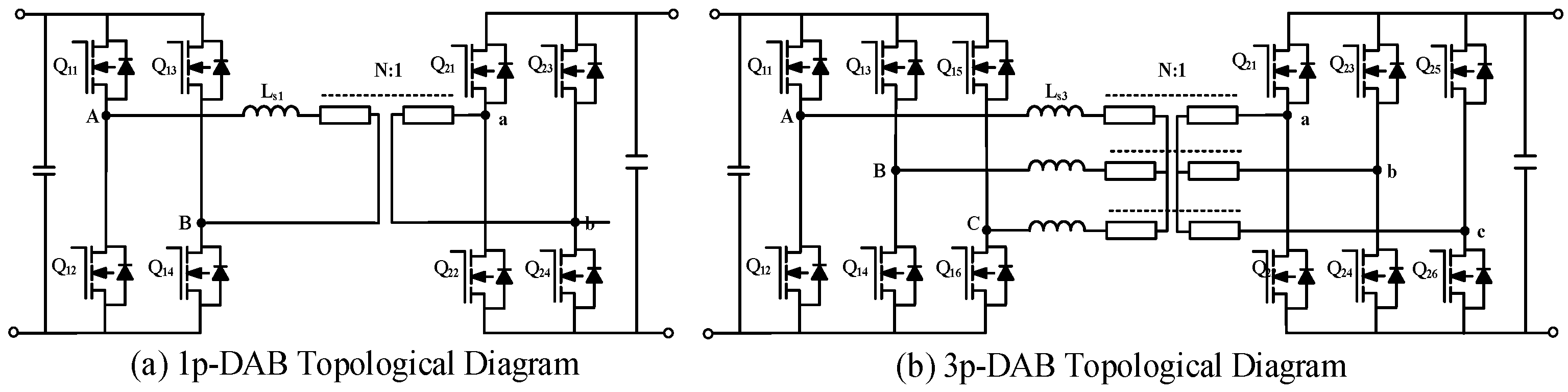
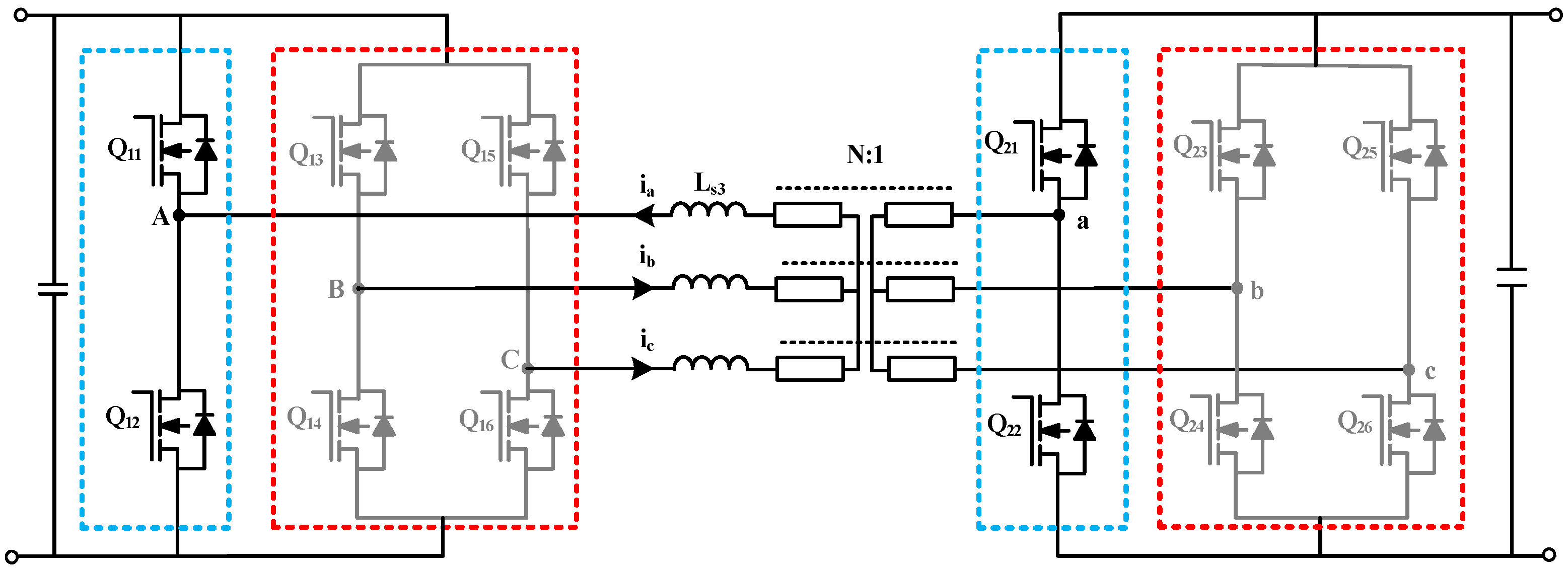
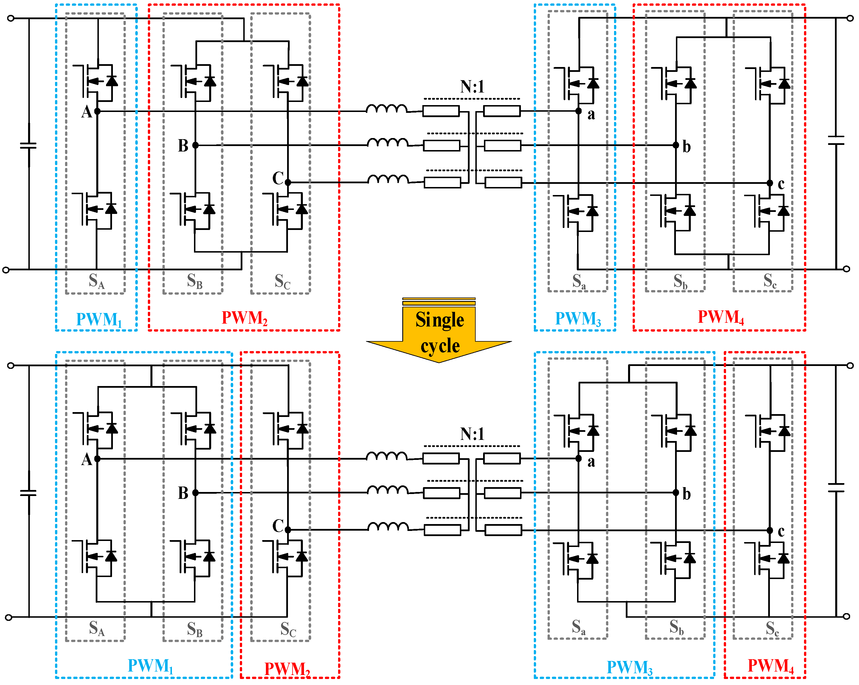
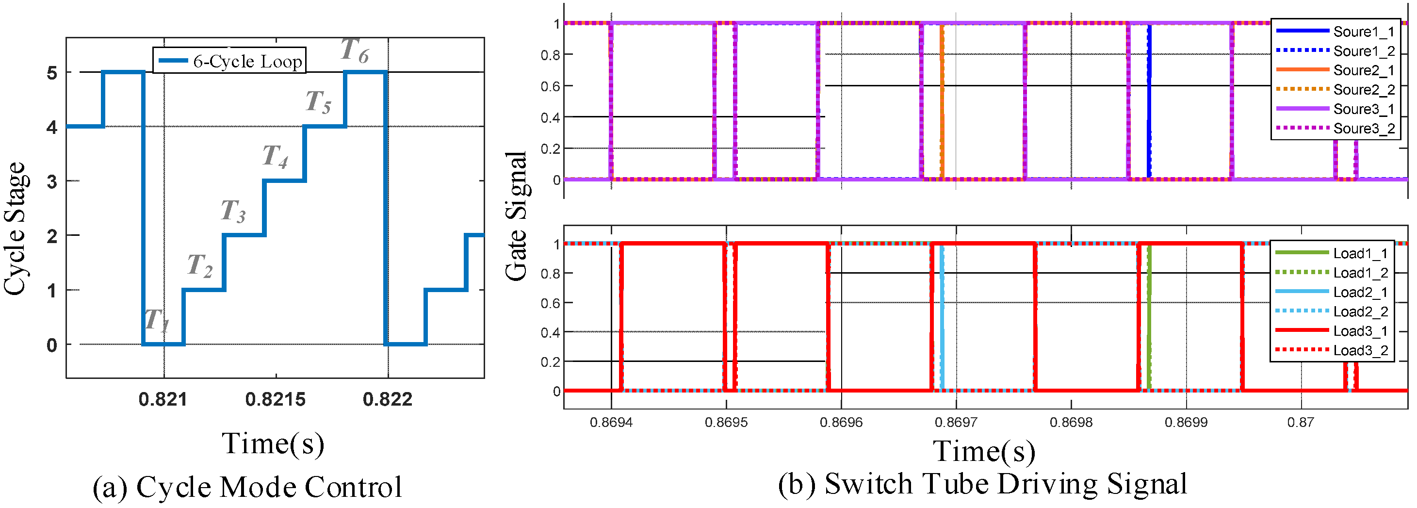
2. Three-Phase, Single-Cycle, Parallel-Cycling Phase-Shifting (3pSPCPS) Mode

2.1. Basic Working Principle of the 3pSPCPS Mode

Research on the control strategy for 1p-DAB is already relatively mature. Despite a slight increase in complexity with TPS control, it achieves the optimization of minimal electrical power stress within the power range and has proven capable of enabling soft switching. The analysis reveals a complementary advantage between these two types of converters, and organically integrating their strengths constitutes the primary research approach of this paper. To enable 3p-DAB to operate in a mode similar to 1p-DAB at medium to low power, this paper introduces a new operating mode based on the topology of 3p-DAB.
Figure 1 presents the schematic topology of 1p-DAB and 3p-DAB. In 3p-DAB controlled by traditional single-phase-shift, the three-phase bridge arms of each 3p-H bridge are shifted by 120°, with a phase-shift angle D between the corresponding bridge arms of the front and back 3p-H bridges. Thus, each pair of corresponding bridge arms can be considered consistent with the SPS modulation of 1p-DAB, allowing 3p-DAB to function as a parallel connection of three single-phase versions. Similarly, 3p-DAB can also be regarded as three 1p-DABs under TPS modulation that are shifted in phase and interconnected. Figure 2 presents a feasible scheme for transitioning from a 3-phase DAB to a 1-phase DAB operation, where the control method adopted is a parallel-phase operation scheme, that is, S B = S C , S b = S c , with a phase difference existing between S C and S B .
In fact, there are many ways to operate 3p-DAB in a mode similar to 1p-DAB, which can be divided from a timeline perspective into non-cyclic and cyclic modes. The non-cyclic mode means that the driving signal for each clock cycle remains unchanged, while the cyclic mode requires exchanging the driving signals of the bridge arms within a certain time period. The cyclic mode can further be divided into fixed-cycle and single-cycle modes. Moreover, based on the topological state of the circuit during single-cycle operation, it can be categorized into a parallel-phase operation and single-phase operation. Table 1 compares the advantages and disadvantages of several feasible schemes for operating 3p-DAB in a manner similar to 1p-DAB.
Comparing the various schemes of operating 3p-DAB in a 1p-DAB mode as presented in Table 1, it is observed that while the single-phase approach is simple and reliable, it suffers from low circuit utilization. Moreover, differential heating due to operational phases can lead to uneven heating of the circuit board, increasing the difficulty of the thermal design in high-power applications. The advantage of the parallel-phase operation lies in the full utilization of the circuit, significantly reducing thermal design challenges. From a timeline perspective, the single-cycle cyclic operation ensures uniform heating across the circuit, easing the design complexity in control. Additionally, influenced by modern switch tube technology, a high degree of symmetry in the parallel phase operation is more achievable. Therefore, this paper adopts a single-cycle cyclic operation with a parallel phase, termed in this study as Three-Phase, Single-Cycle, Parallel-Cycle Phase-Shifting (Three-phase, single-cycle, parallel-cycle, 3pSPCPS).

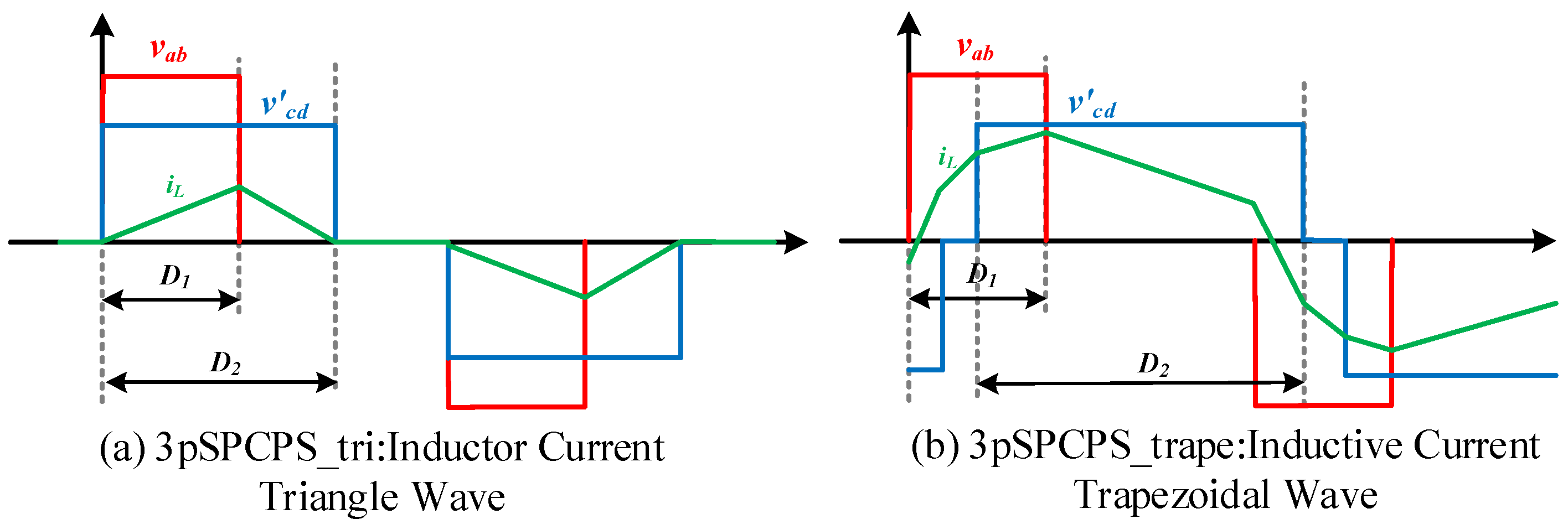
2.2. Detailed Analysis of 3pSPCPS Applied to DAB

Although the previous section introduced a basic concept for operating 3p-DAB in a manner similar to 1p-DAB, there are some issues in the actual design, including how and when to switch. This section primarily focuses on these specific details, analyzing and explaining them to address the challenges of 3pSPCPS in practical applications.
(1)
The Concept of Switching
The control of the 1-phase DAB can be divided into four groups of P W M waves to control four bridge arms. For ease of explanation, the bridge arms are numbered 1, 2, 3, and 4 from the primary to the secondary side. It is defined that P W M X , X 1,2 , 3,4 = 1 means the upper tube of the corresponding X bridge arm is turned on and the lower tube is turned off; P W M X , X 1,2 , 3,4 = 1 means the upper tube of the corresponding X bridge arm is turned off and the lower tube is turned on. The control of the 3-phase DAB can be divided into six groups of PWM waves for controlling six bridge arms. The three-phase bridge arms of the front bridge are defined as A, B, and C, and those of the rear bridge as a, b, and c. It is defined that S X , X A , B , C , a , b , c = 1 means the upper tube of the corresponding X bridge arm is turned on, and the lower tube is turned off; S X , X A , B , C , a , b , c = 0 means the upper tube of the corresponding X bridge arm is turned off, and the lower tube is turned on. Since there is only a delay between the corresponding tubes of the front and rear bridges, the analysis can be limited to the state of the front bridge for switching purposes. The operations of the rear bridge corresponding to the front bridge arms are consistent, with only a certain delay.
The DAB operation in the 3pSPCPS mode requires providing two types of modulation waves for the front bridge, similar to the modulation waves under TPS control of the single-phase Dual Active Bridge DC converter. For 3p-DAB, the front bridge has three bridge arms requiring three types of modulation waves (i.e., S A , S B , S C ). For ease of analysis, P W M 1 and P W M 2 can be considered fixed, and the 3pSPCPS modulation can be seen as distributing the three modulation waves S A , S B , S C to the two types P W M 1 and   P W M 2 in a single-cycle, parallel-phase cycling manner.
(2)
Switching State and Sequence
The 3pSPCPS control requires a switch at every clock cycle, with Figure 3 showing the operational state of the switch tubes at moments T 1 and T 2 . At T 1 , the driving signal for the first bridge arm is P W M 1 , while the second and third bridge arms operate in parallel phase with a P W M 2 signal. At T 2 , the first and second arms operate in parallel phase with a P W M 1 signal, and the third arm receives a   P W M 2 signal, with only one phase-shift operation occurring between the two moments, that is, a phase shift of S C . The post-switch state and sequence of states in 3pSPCPS are not arbitrary and require consideration of the following issues:
Switching State: It is necessary to ensure that within a large cycle period under steady state, the duration and state of each switch are the same. This uniformity allows for consistent utilization of all switches, thereby ensuring even heating.
Switching Sequence: Each switch state will involve a phase-shifting operation, with the requirement that the fewer phase-shifting operations during switching, the better. This helps to reduce the loss during commutation and the EMI generated during phase-shifting.
Taking into account the above two issues, this paper presents a reasonable and feasible switching state and sequence as shown in the Table 2. It can be seen that within a large clock cycle, there are six states, with only one phase-shifting operation occurring in each state transition (as indicated by the purple mark), and the operation of each switch, aside from a certain delay, is the same. This ensures uniform heating of all switches and effectively reduces the electromagnetic interference caused by phase-shifting during each clock cycle switch.
(3)
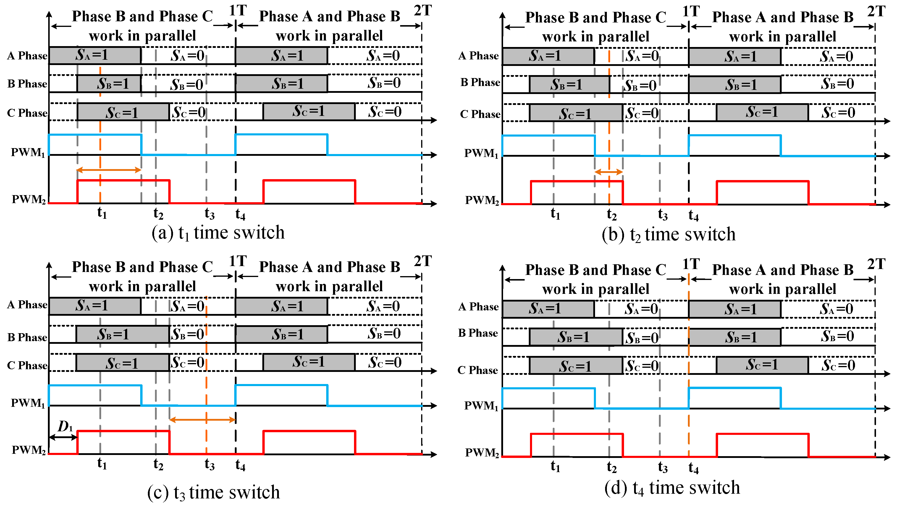
Switching Time Points
After determining the switching state and sequence for each cycle, the specific switching moments within the cycle need to be identified. The analysis continues with the transition from parallel phases B, C to A, B as shown in Figure 4, presenting four typical switching time nodes. The impact of these four switching times on control is analyzed next:
  • Choosing time node t 1 for switching from phase P W M 2 to P W M 1 for B, even though no switch tube operation occurs, the duty cycle of B within T is not 50%, leading to a DC bias issue at the switching moment.
  • At time node t 2 , switching from 6 back to P W M 1 instantly changes B’s state from S B = 0 to S B = 1 , resulting in additional switching losses. Similarly, the duty cycle of B within T not being 50% introduces a DC bias issue.
  • Selecting time node   t 3 and switching from P W M 2 back to P W M 1 for B, B’s state instantly remains at S B = 0 , avoiding additional switching losses. Moreover, with B’s duty cycle within T remaining at 50%, DC bias issues are prevented.
  • By choosing time node t 4 for switching from P W M 2 back to P W M 1 , both A and B’s states instantly change from S A = 0 to S A = 1 , causing extra switching losses. However, B’s duty cycle within T still being 50% prevents DC bias issues.
Figure 4. Four typical switching time node operations.
Processes 13 01921 g004
Upon comprehensive analysis of the circuit operational effects at the four typical switching times, employing interval t 3 for switching results in the circuit operating in an optimal state. This paper selects the midpoint of the interval t 3 as the switching moment, corresponding to
t 3 = ( D 1 4 + 3 4 ) T
In Equation (1), D 1 denotes the duty ratio of the switching signal during one cycle, and T represents the full duration of a switching cycle.

3. Standardized Global Unified Operation Strategy Under Wide Voltage Range

3.1. Wide Voltage Range Optimization Scheme at Low and Medium Power Levels

The 3pSPCPS mode is applied to 3p-DAB operating at medium and low transmission powers to optimize minimal reverse power and enable soft switching at medium and low powers, similar to the operating state of 1p-DAB under TPS modulation. Section 2.1 analyzes the operating characteristics and optimization of 1p-DAB under TPS modulation, presenting an optimized scheme for step-down 1p-DAB in forward transmission mode. To achieve minimal current stress optimization, the conclusion is to use Mode3A at low power and Mode4B at high power. Other modes will not be considered in this paper due to their inability to meet the optimization criteria. Following the analysis in this paper, DAB operating conditions are divided into four categories based on power range (defined as P ower 1 , P ower 2 , P ower 3 , and P ower 4 , respectively), with this section focusing on optimization schemes for medium and low power. Based on the analysis in Section 2, the optimization scheme for step-down power transmission is presented directly as shown in Table 3.
Figure 5 shows the circuit basic switch current waveforms under two working conditions, P ower 1 and P ower 2 . It can be seen that the inductor current waveform is a triangular wave under the P ower 1 working condition and soft switching can be achieved. Therefore, the working mode at this time is defined as 3 p S P C P S _ t r i . Under the P ower 2 working condition, the inductor current waveform is a trapezoidal wave, and soft switching can also be achieved. The working mode at this time is defined as 3 p S P C P S _ t r a p e .
To satisfy the requirements for a wide voltage range, this section provides an optimization scheme for forward power transmission with a voltage gain greater than 1. Analyzing the waveforms in Figure 5, the voltage and inductor current are symmetrical during the step-up and step-down phases, with output power and cyclic power being identical. This allows for a similar transformation to propose an optimization scheme for boost operation in forward power transmission.
d ^ = 1 / d v ^ a b = v c d v ^ c d = v a b D ^ 1 = D 2 D ^ 2 = D 1 D ^ 3 = D 2 + D 3 D 1
In Equation (2), v ^ a b and v ^ c d denote the equivalent voltages on the primary and secondary sides of the transformer, respectively. d is the voltage gain, D 1 and D 2 are the primary- and secondary-side duty ratios under the current operating mode, and D 3 is introduced as an equivalent normalized duty ratio, providing a unified expression for power transfer analysis across the primary and secondary sides. Its equivalent transformation satisfies the Equation (2). The forward boost optimization scheme obtained after the transformation is shown in Table 4.
The optimization control scheme can be further simplified by changing the per-unit value to Equation (3), resulting in a simplified optimization control scheme for forward medium and low power transmission over a wide voltage range, as shown in Table 5.
I b = V 1 4 f L S 1 , P b = V 1 2 2 f L S 1
In Equation (3), the input voltage V 1 , series inductance L S 1 , and switching period f are used to define the power and current base values for the normalization process. The base current I b and base power P b are fundamental references for the per-unit control design.

3.2. Control Scheme for Wide Voltage Range Under High-Power Conditions

To facilitate standardized comparative analysis, the per-unit value is adopted as I b = V 1 T s / 4 L s 3 , P b = V 1 2 T s / 2 L s 3 , and the maximum value of the duty cycle D is constrained to 1/2. The per-unit normalized expression of the power transfer characteristic is thus given by Equation (4):
P 3 p S P S = 2 d D 3 p S P S 3 d D 3 p S P S 2 2 0 D 3 p S P S 1 3 3 d ( D 3 p S P S D 3 p S P S 2 ) d 6 1 3 D 3 p S P S 1 / 2
By solving the above equation, the relationship between the phase-shift angle D 3 p S P S , the transmitted power P n , and the gain d under the forward high transmission power condition for the 3p-DAB is obtained as Equation (5). The corresponding control table under this condition is shown in Table 6.
D 3 p S P S = 2 3 1 3 4 6 P n d 0 P n d / 2 1 2 1 2 7 9 4 P n 3 d 0 d / 2 P n 7 d / 12

3.3. Standardized Unification Based on Virtual Phase-Shift Ratio

(1)
Correction of Operating Range under Medium- and Low-Power Conditions
The per-unit expressions for medium/low power and high power are structurally similar. However, it is evident that under medium- and low-power conditions, employing the 3pSPCPS control strategy alters the 3p-DAB topology, making it not entirely equivalent to a 1p-DAB. The most significant difference lies in the use of parallel phase operation, which changes the effective inductance of the circuit. Considering the symmetry of the leakage inductances in the three phases of the 3p-DAB, the leakage inductance for each phase is defined as L s 3 = L . When the 3p-DAB operates under the 3pSPCPS mode, the effective leakage inductance satisfies the following relationship:
L s 1   =   1.5 L s 3   =   1.5 L
Therefore, it is necessary to correct the operating range under medium- and low-power conditions. After correction, the applicable power range is as specified in Table 7. It should be noted that the power correction affects only the boundary expressions of the operating conditions and does not impact the optimization strategies across different operating scenarios.
(2)
Expanding the Meaning of the External Phase-Shift Ratio D f
Based on the above analysis, operating conditions are divided based on voltage gain and power range. Generally, the voltage gain is known, but the power range needs to be detected. Due to the effects of system output capacitor charging and discharging as well as detection delay, changes in detected power are lagging. Directly dividing operating conditions based on detected power presents the following disadvantages:
  • Slow dynamic response, with ringing occurring under input and load disturbances.
  • Mode switching under multiple conditions can oscillate due to the lagging effect of power.
  • It may affect system stability, requiring higher stability margins for the control system.
Therefore, directly using detected power for dividing operating conditions and optimizing control in the control system is not an optimal solution. In forward transmission mode, its value range is [0, 0.5], with a larger amplitude corresponding to a higher transmission power. For 3p-DAB under 3pSPS control, there are no D and F, nor is there the concept of the external phase-shift ratio. However, there is a phase-shift angle D 3 p S P S , which is also related to the DAB‘s transmission power, with a value range of [0, 0.5] in forward transmission mode. Furthermore, the value ranges of D f and D 3 p S P S overlap, making them unsuitable as references for mode switching. To this end, this paper extends the traditional meaning of D f in 1p-DAB to the full power range of 3p-DAB (defined as the virtual phase-shift ratio D f ). After the extension, the value range is [0, 1]. Through the virtual phase-shift ratio, the power aliasing between modes can be solved, which is beneficial for mode identification and reduces the complexity of the optimal control expression. In the 3pSPCPS mode, the D f value range is [0, 0.5], while in the 3pSPS mode, the D f value range is [0.5, 1]. Additionally, a virtual relationship is established, satisfying the equation:
D f = D 3 + D 2 / 2 D 1 / 2 D 1 = 0 , D 2 = 0 D 3 p S P S = f ( D 3 ) D f ( 0.5 , 1 ]
Here, f ( D 3 ) represents the functional relationship between D 3 p S P S and D 3 in the 3pSPS operating mode.
(3)
Unification of Reference Quantities Across the Full Power Range
Based on the above analysis, this paper selects D f as the control reference quantity within the full power range. The critical step towards unification is to establish the relationship between D 3 p S P S and D f , that is, to solve for f ( D 3 ) . A pivotal issue addressed is the power overlap problem under the two operating modes.
Here, the analysis is conducted in step-down mode, while the step-up mode can be derived similarly. P M _ 1 p-DAB = 0.25 d represents the maximum transmission power under the condition P o w e r 2 , and it has been calculated that the power point falls within the quasi-high power range, satisfying the expression G.
P n = P M _ 1 p-DAB = d 4 D 3 p S P S = 2 3 1 3 4 6 P n d
Solving the above expression yields the boundary solutions for the two mode transitions as
D b o u n d a r y _ 3 p S P S = 2 3 10 6
Due to the substantial overlap in the power range, the adjustable range of D f within the high power range is less than 0.5. Therefore, transformation expression (10) is introduced to extend D f s range to 1, thus establishing the relationship between D f and D 3 p S P S under 3pSPS control.
D f = D 3 p S P S D b o u n d a r y _ 3 p S P S 0.5 0.5 D b o u n d a r y _ 3 p S P S + 0.5
The inverse function is obtained as follows:
D 3 p S P S = D f 0.5 0.5 D b o u n d a r y _ 3 p S P S 0.5 + D b o u n d a r y _ 3 p S P S    
Under high-power operation, two additional operating modes exist. To partition the operating conditions, it is likewise necessary to determine their power boundary, which is defined by the following expression:
P n = P b o u n d a r y h i g h p o w e r i n t e r m e d i a t e s t a t e = d 2 D 3 p S P S = 2 3 1 3 4 6 P n d
Solving for D 3 p S P S = 1 / 3 and substituting into the transformation formula yields the power boundary:
D f = 0.5 + 10 2 2 ( 10 1 )
Therefore, based on the value of D f , the full power range is divided into four operating conditions as shown in Table 8:

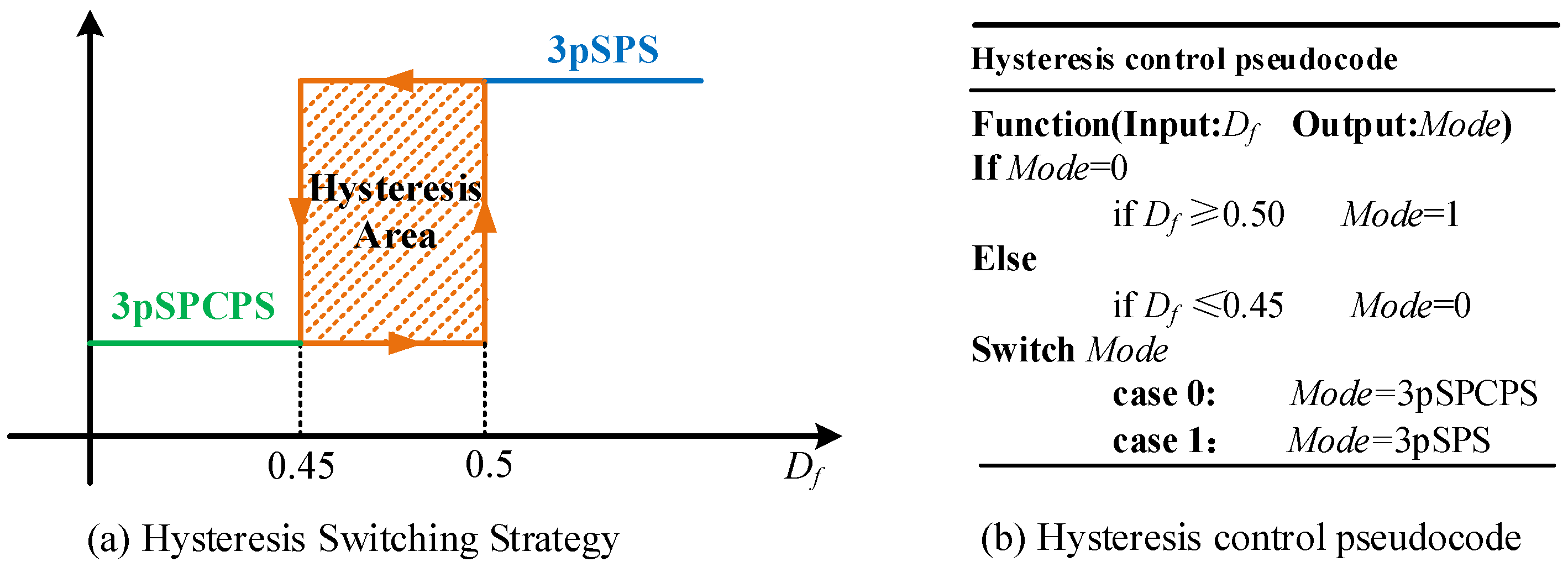
3.4. Global Operational Improvement Strategy to Suppress Switching Oscillations

In response to the demands of a wide voltage range, a mode-switching scheme is employed. Due to requirements or disturbances, the system may frequently switch modes across various conditions. To minimize the impact of mode-switching oscillations, the system’s mode switches can be classified into three types, with the corresponding solutions as follows:
(1)
Oscillations during switching between  P o w e r 1 and  P o w e r 2 as well as  P o w e r 3 and P o w e r 4 are caused by changes in the mid-segment  D f of the control optimization algorithm. Since D f is a continuous function during the switch, the impact of oscillations is minimal and can be largely ignored; thus, no further action is taken in this paper.
(2)
Oscillations during the switch between medium and low power in d < 1 and d 1 are caused by changes in the input  d of the control optimization algorithm. The switching of  d can result in discontinuous branch structures in the optimization algorithm, potentially leading to severe oscillations. At medium and low power, it has been found that soft switching can be achieved under any gain using SPS control when  d = 1 , and the system reliability is very high. Therefore, this paper designs a high-reliability buffer zone in the prone-to-oscillation area, with a specific scheme to operate under SPS control when 0 . 95 d < 1 . 05 .
(3)
Oscillations between P o w e r 2 and P o w e r 3 at medium to low power are caused, on the one hand, by the influence of Df, leading to discontinuous branch structures in the optimization algorithm, and, on the other hand, by the mode switch altering the circuit’s topology, thus causing severe oscillations. This paper employs hysteresis control to suppress such oscillations.
The previous analysis identified the power boundaries for 3pSPCPS and 3pSPS as D f = 0 . 5 . Given that the upper power limit of the converter under 3pSPCPS control corresponds to D f = 0.5 , the chosen hysteresis region should be less than 0.5. However, a hysteresis region that is too large is detrimental to the optimized operation of the converter. This paper selects the hysteresis region as 0 . 45 , 0 . 5 , and Figure 6 presents the schematic diagram of hysteresis control switching and its pseudocode for control. When the DAB operates in 3pSPCPS mode and D f 0 . 50 is detected, the system will switch to the 3pSPS working mode; when the DAB operates in 3pSPS mode and D f 0 . 45 is detected, the system will switch back to the 3pSPCPS working mode. The introduction of hysteresis control effectively suppresses oscillations caused by mode switching.
Although the optimization scheme introduces a hysteresis zone, analysis has found that the power range corresponding to D 0.45,0.5 still falls within the adjustable interlaced power range of 1p-DAB and 3p-DAB, thus the formula does not require correction. After introducing strategies to suppress mode-switching oscillations, the improved control scheme under the requirement for wide boost is shown in Table 9. For cases where the gain under forward power transmission is greater than 1, the reader can derive the conclusion themselves using the analysis process mentioned above. This paper directly presents the conclusion.

4. Analysis of DAB Operational Characteristics Under Multiple Working Modes
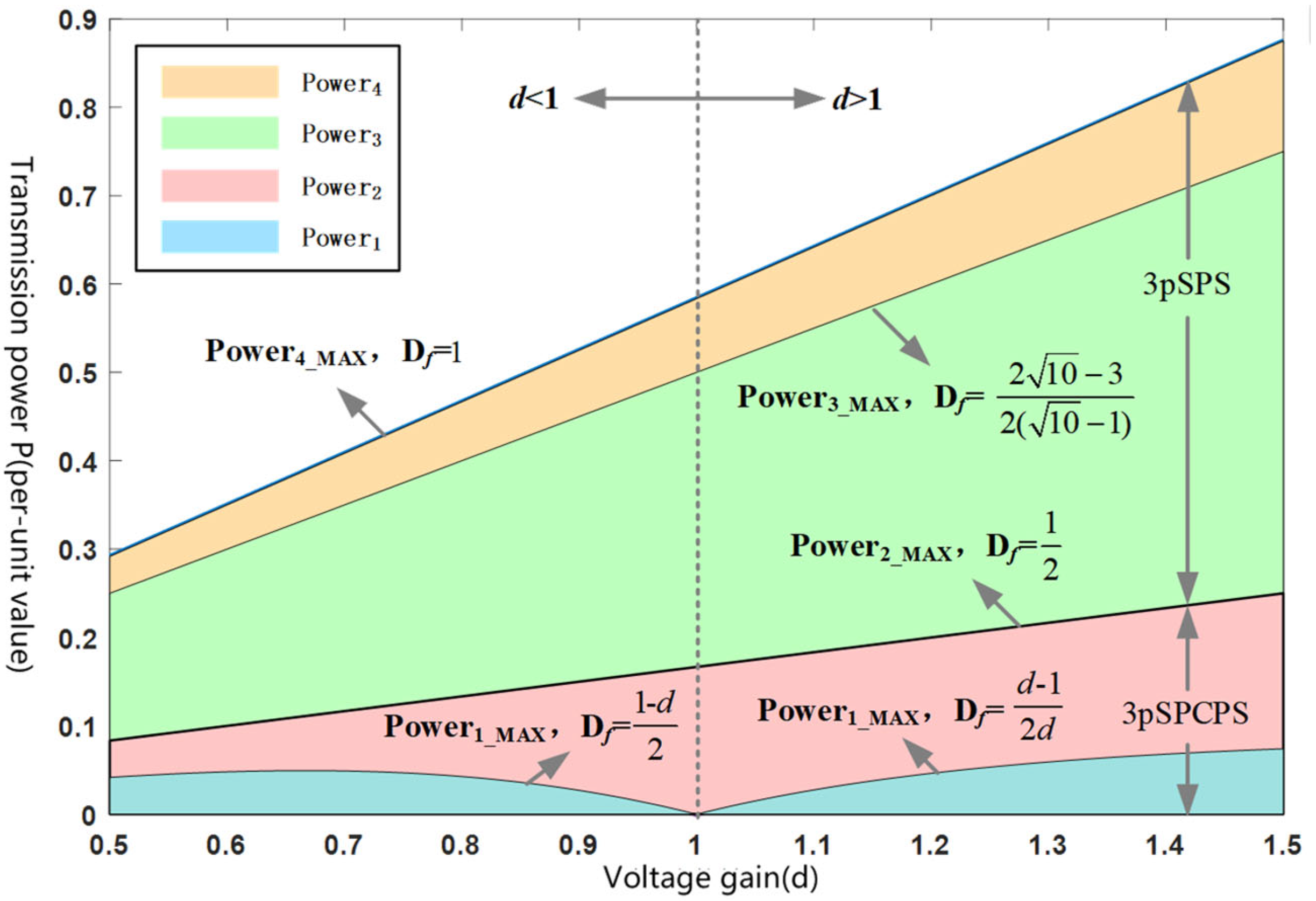
The previous section presented a standardized, unified operational strategy. This section focuses on analyzing the operational characteristics of said strategy. Considering the need for a wide voltage and power range, this paper categorizes the operational states of the 3p-DAB into low power range, medium power range, quasi-high power range, and high power range (corresponding to P o w e r 1 , P o w e r 2 , P o w e r 3 , and P o w e r 4 , respectively), with operational control modes divided into 3pSPCPS and 3pSPS. The following analysis will primarily address power characteristics and soft-switching features.
(1)
Power Characteristics Analysis
Figure 7 presents the division of the full power range into four operating conditions ( P o w e r 1 to P o w e r 4 ), along with the corresponding control modes ( 3 p S P C P S _ t r i , 3 p S P C P S _ t r a p e , and 3pSPS) and their mapping to different regions of the normalized power index D f , where the per-unit value P n satisfies Equation (3). The power coverage range of the traditional 1p-DAB includes P o w e r 1 and P o w e r 2 , while that of the traditional 3p-DAB encompasses P o w e r 1 , P o w e r 2 , P o w e r 3 , and P o w e r 4 . However, optimization is not achievable due to limitations in control flexibility. This paper utilizes two hybrid control strategies, 3pSPCPS and 3pSPS, with P o w e r 1 adopting 3 p S P C P S _ t r i control to primarily achieve the optimization objective of minimal current stress and, secondarily, the optimization objectives of minimal reverse power and minimal RMS; P o w e r 2 employs 3 p S P C P S _ t r a p e control to achieve the optimization objective of minimal current stress; P o w e r 3 and P o w e r 4 are controlled by 3pSPS to maintain high power operation. Thus, the operational scheme proposed in this paper not only retains the high-power transmission characteristics of the 3p-DAB under wide voltage conditions, but it also achieves optimization objectives at medium and low power levels.
(2)
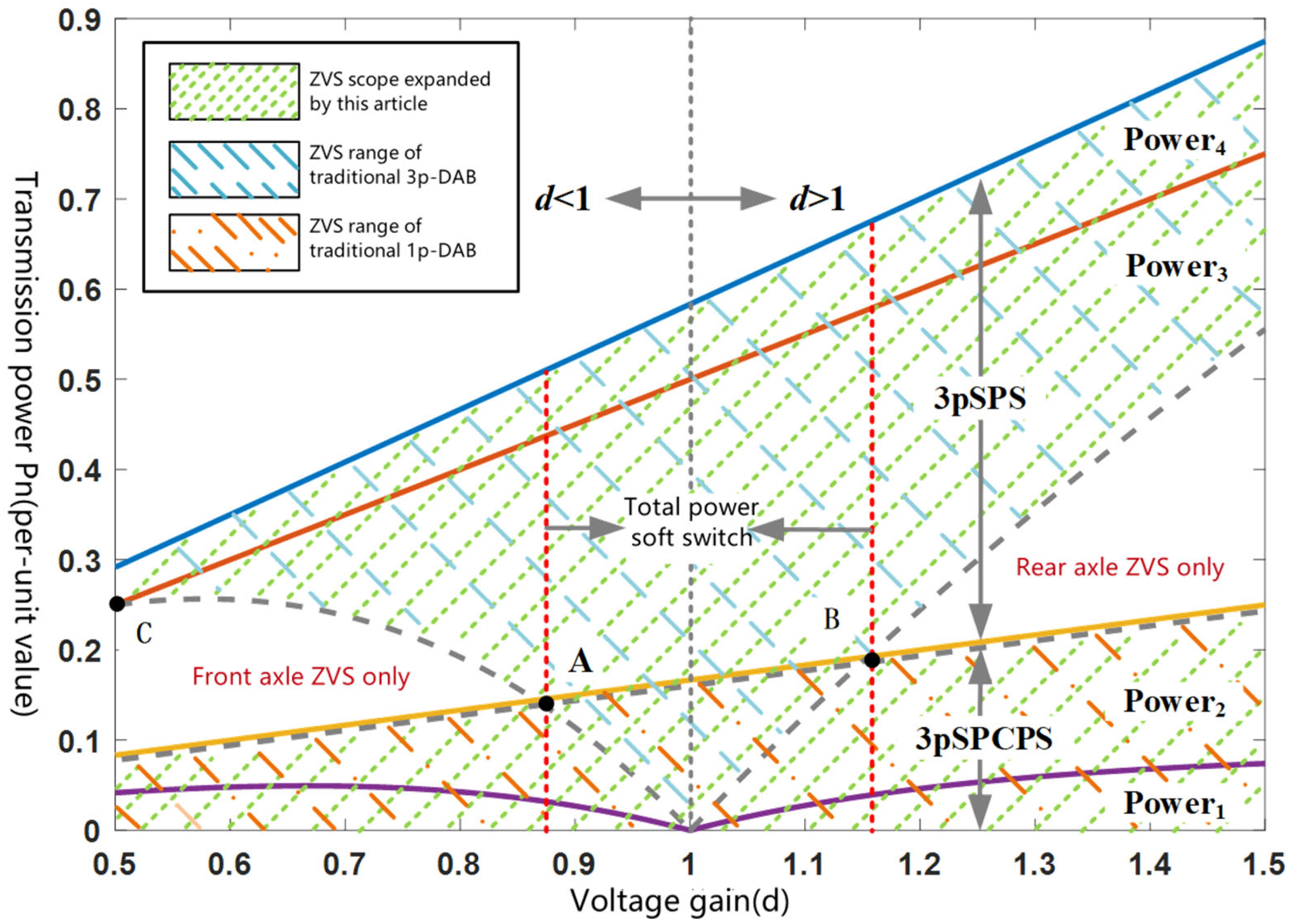
Soft-Switching Characteristics Analysis
Figure 8 displays the soft-switching region diagram across the global power range under wide voltage conditions, where the per-unit value P n satisfies Equation (3). As shown in the figure, the blue region represents the ZVS range achievable by conventional 3p-DAB control, which is mainly concentrated in the high-power region. Under conventional control, the soft-switching range of the 3p-DAB is very narrow at medium and low transmission power levels, and it becomes even more limited as the voltage gain deviates from 1. Full-range ZVS can only be achieved when d = 1 . The yellow region denotes the ZVS coverage typically realized by TPS-optimized, single-phase DAB (1p-DAB) within its operating power range. The green region indicates the extended ZVS region enabled by the proposed multi-mode control strategy. With the implementation of our strategy, the ZVS capability of the 3p-DAB is significantly expanded into the medium- and low-power regions under a wide voltage range, while the soft-switching characteristics in the quasi-high-power and high-power regions are well preserved. To support the soft-switching design of the converter, the key operating points A, B, C, and D in the ZVS region are further analyzed. Note that point D is not shown in the figure due to scale limitations.
Points A and B: As shown in the figure, the operating region between points A and B can achieve soft switching across the full power range. In the soft-switching design, the voltage gain should overlap with this range as much as possible to reduce the switching losses of the converter. The expression for point A is as follows:
2 3 D 3 p S P S 2 = d 2 d D 3 p S P S 3 d D 3 p S P S 2 2 = d 6
The solution yields that the duty ratio ( d ) corresponding to point A is 3 / 2.
The expression for point B is as follows:
2 3 D 3 p S P S 2 1 = d 2 d D 3 p S P S 3 d D 3 p S P S 2 2 = d 6
The solution yields that the duty ratio ( d ) corresponding to point B is 2 3 / 3 .
Therefore, it is recommended to design the voltage gain in the range of 3 / 2 2 3 / 3 to meet the soft-switching characteristics across the full power range.
(3)
Points C and D: As shown in the figure, points C and D are the intersections of the upper power limit of Y and the soft-switching boundary. When the duty ratio (d) is less than the gain corresponding to point C or greater than the gain corresponding to point D, all soft-switching characteristics are lost below Y, with an extremely narrow range of soft-switching across the full power range. Unless specifically required by the design, it is not recommended to set the voltage gain within this range. The expression for point C is as follows:
2 3 D 3 p S P S 2 = d 2 d D 3 p S P S 3 d D 3 p S P S 2 2 = d 2
The solution yields that the duty ratio (d) corresponding to point C is 1 / 2 .
The expression for point D is as follows:
2 3 D 3 p S P S 2 1 = d 2 d D 3 p S P S 3 d D 3 p S P S 2 2 = d 2
The solution yields that the duty ratio (d) corresponding to point D is 2, but due to scale limitations, this point is not shown in Figure 8.
Therefore, it is not recommended to set the voltage gain in a range less than 0.5 or greater than 2.
In summary, when d 0.5 , 2 , the converter can achieve zero-voltage switching (ZVS) and minimum current stress optimization under the P o w e r 1 and P o w e r 1 conditions, and ZVS can still be achieved under the P o w e r 3 condition. Moreover, when d 3 / 2 , 2 3 / 3 , ZVS remains achievable under the P o w e r 4 condition. Compared with traditional PS control, which achieves full-range ZVS only when d = 1 , the proposed multi-mode control strategy significantly expands the ZVS region and optimization space toward the medium and low power range.

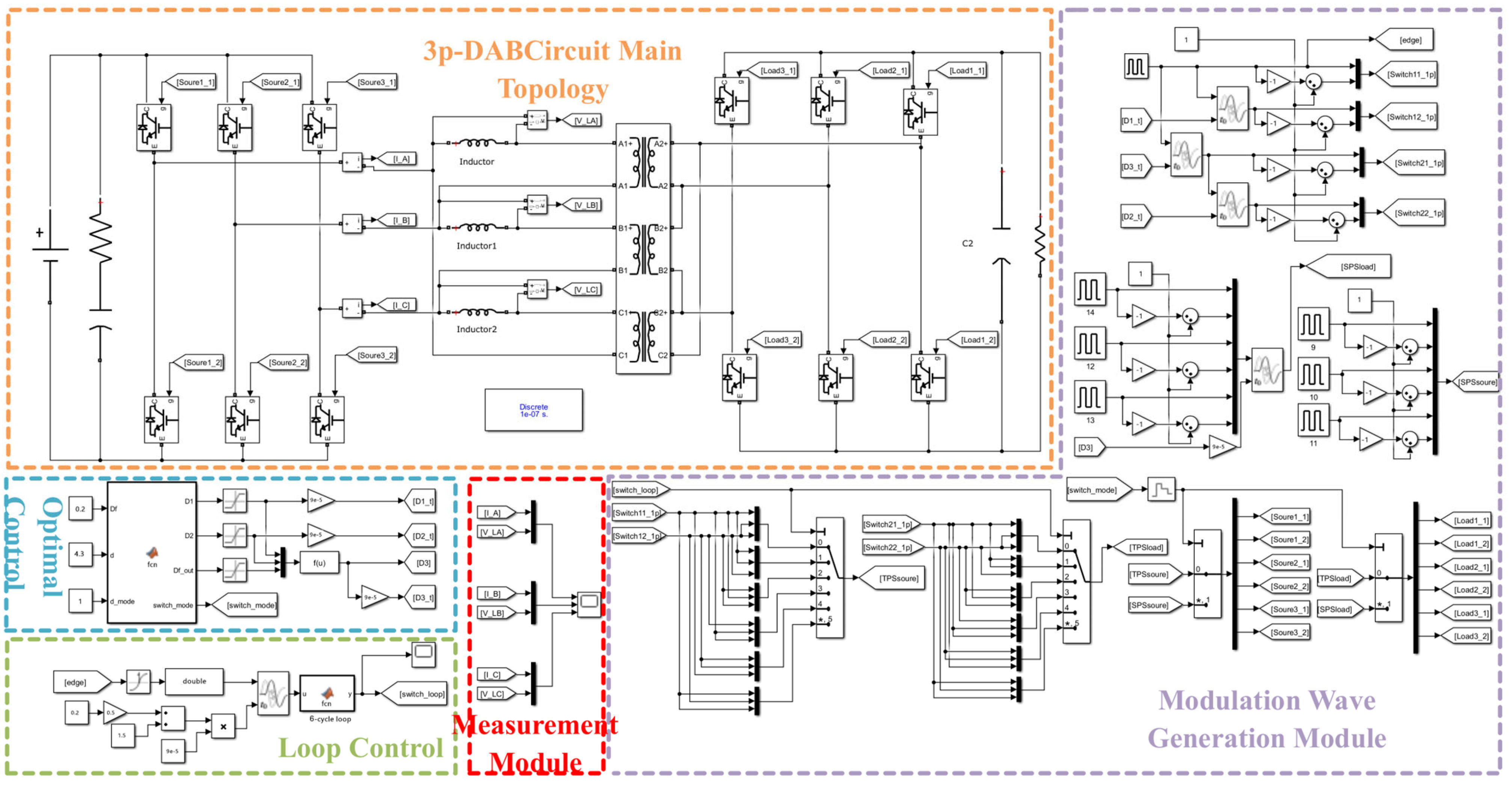
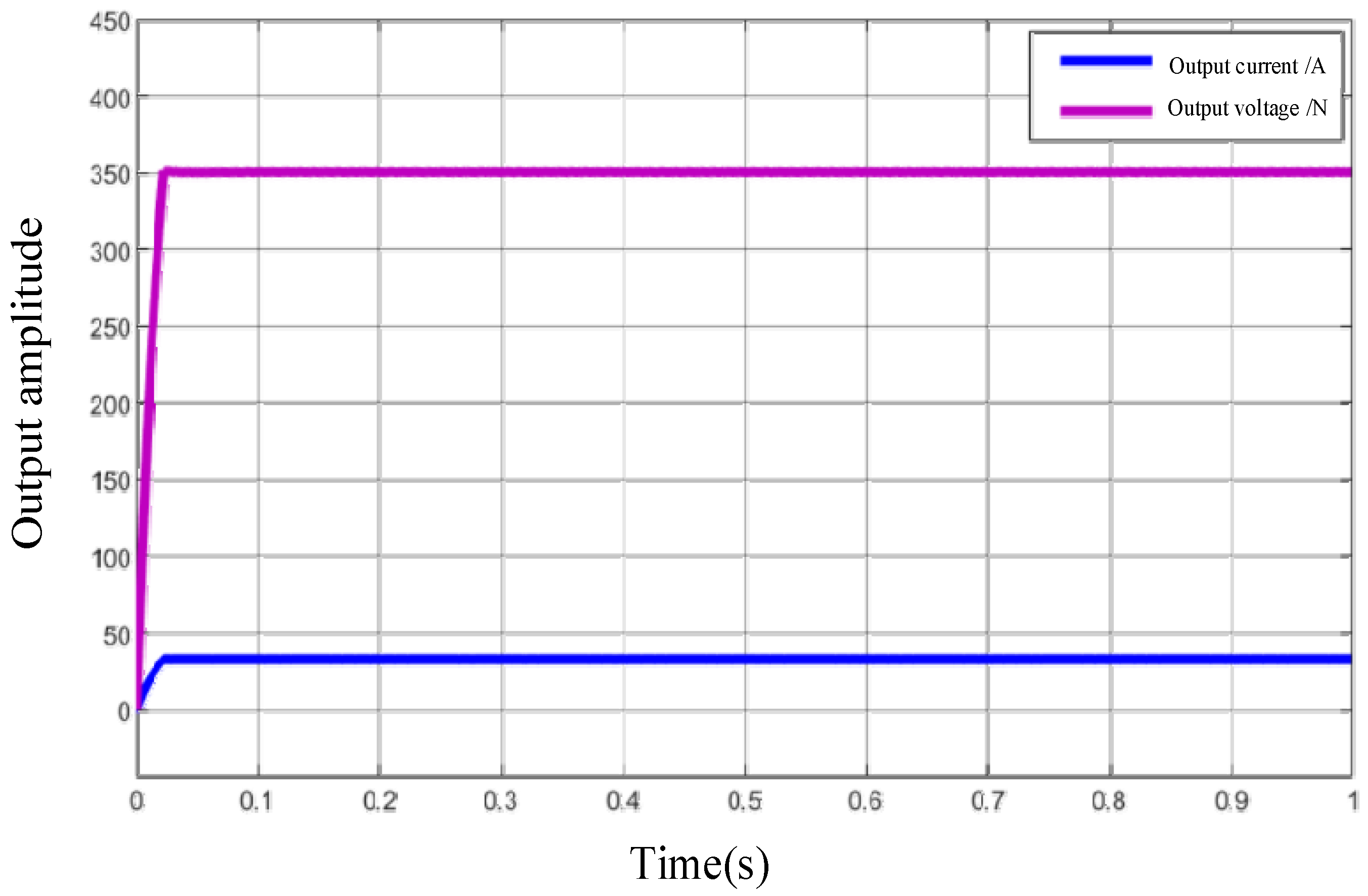
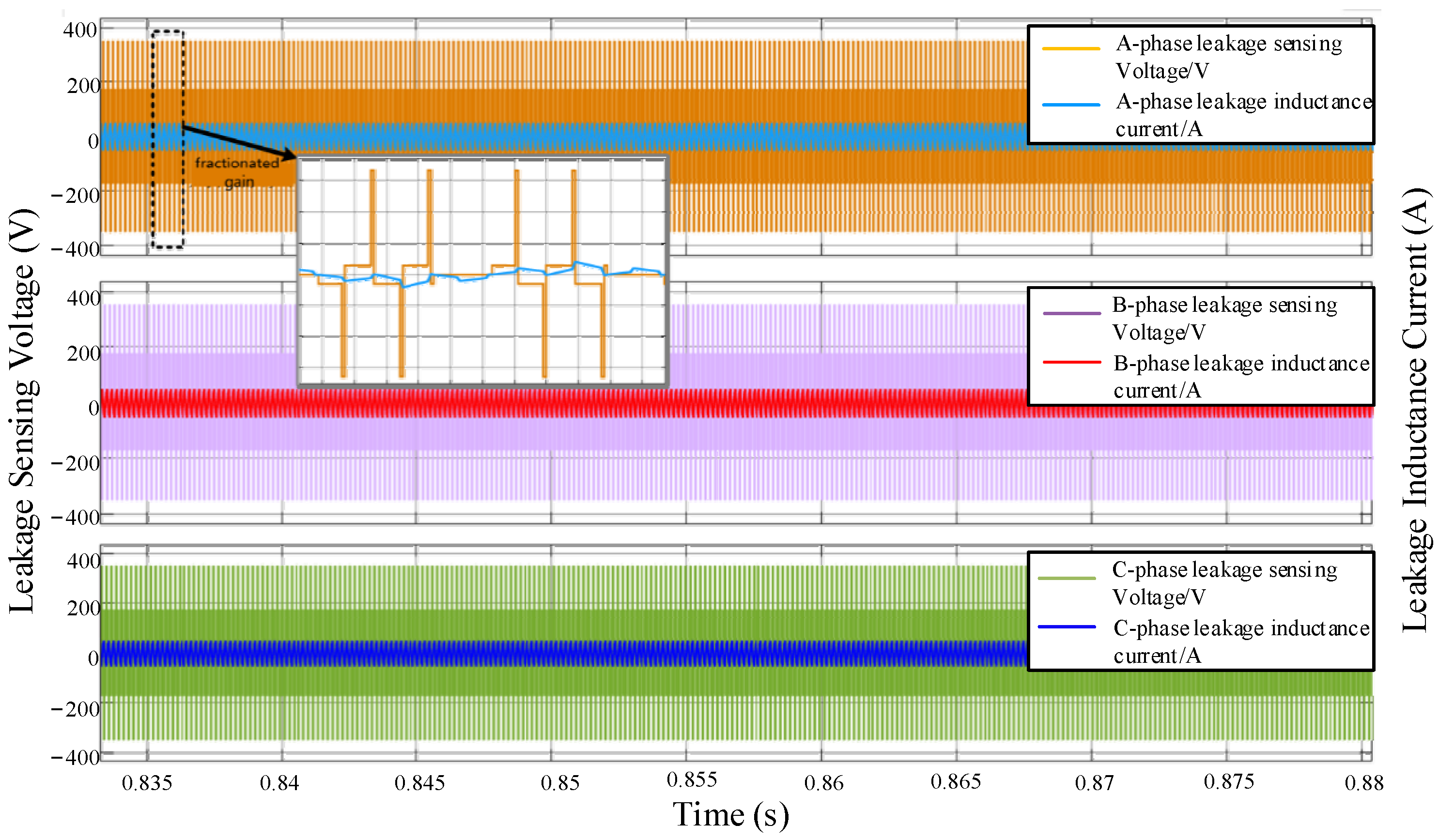
5. Simulation Verification

To verify the correctness of the multimodal switching operation management scheme of the 3p-DAB proposed under a wide voltage range, this paper constructs a simulation model of a three-phase Dual Active Bridge converter on the Matlab / Simulink platform (https://www.mathworks.com/products/simulink.html accessed on 15 May 2025), as shown in Figure 9. The simulation model employs an open-loop control scheme, facilitating the analysis of the 3p-DAB’s operation. The overall model comprises five parts: the 3p-DAB circuit’s main topological unit, optimization control unit, loop control unit, measurement module unit, and modulation wave generation module unit, with the simulation circuit parameters shown in Table 10.
The proposed control strategy is not limited to a specific converter configuration. It is applicable to various three-phase DAB systems used in practical scenarios, such as vehicle-to-vehicle energy sharing and microgrid interfacing. To reflect real-world application needs, the converter parameters in the experiment are selected based on typical engineering requirements rather than theoretical constraints.
For the 3p-DAB designed for a wide voltage range, this section initially proposes the 3pSPCPS operating mode at medium to low power to achieve similar operational effects to the 1p-DAB. Therefore, this section will first verify the operational effects of the 3p-DAB under this mode and the feasibility of the implementation method. Additionally, the 3p-DAB employs a multimodal operation management approach under four different conditions, so this section will also verify the operational effects of the circuit under multiple modes. The following will detail the simulation situations for these two aspects.
(1)
Simulation Verification of the Implementation Effectiveness and Feasibility of the 3pSPCPS
Operating Mode
This simulation employs an open-loop verification method, setting the voltage transfer ratio d to 1, the shift ratio D f to 0.1, and the output load power to 10 kW. Figure 10 displays the output results of the 3p-DAB under the 3pSPCPS operating mode. From the output results, it can be observed that the output voltage is stable at 350 V, and the output current is stable at 28.6 A, consistent with the theoretical analysis of the 3pSPCPS operating mode.
The implementation of the 3 p S P C P S operating mode relies on the generation of the correct modulation wave. A critical step is the production of a time cycle control state signal (generated by the cycle control unit shown in Figure 9), as depicted in Figure 11a, where the state information M o d e 0 , 1 , 2 , 3 , 4 , 5 of a modulation wave changes with each clock cycle. The switching information corresponding to the control in Figure 11a is consistent with the design presented in Table 2. The value corresponding to this mode is then transmitted as a switching control quantity to the modulation wave generation module unit, thereby generating the gate drive signal shown in Figure 11b, and the waveform of this drive signal is consistent with the theoretical design of the 3pSPCPS operating mode.
Based on the standardized global unified operation scheme shown in Table 9, with d [ 0.95 , 1 ] , this precisely corresponds to the 3pSPCPS operating mode under medium to low power (where the 3p-DAB operates in a manner similar to 1p-DAB controlled by SPS). The voltages across the three-phase leakage inductances and the currents flowing through them, as shown in Figure 12, are highly symmetrical across the three phases, with only a 120° phase-shift present. Furthermore, according to the close-up view, the waveform of the voltage across the inductance and the current, as well as their relationship, conform to the theoretical analysis of DAB operation.
The operational effect of the 3 p S P C P S mode can be directly analyzed from the waveform of the three-phase current, with the simulated waveform of the current flowing through the three-phase leakage inductance provided in Figure 13. For each single-phase current, 6T constitutes a cycle. According to the simulation results, i b lags i a by 120°, and i c lags i b by 120°, which conforms to the relationship of the three-phase current in 3p-DAB. During the T 1 cycle, the current relationship satisfies i b = i C , i a = ( i b + i C ) , thus aligning with the analysis of the BC phase parallel operation within the T 1 cycle as per Table 2. A similar analysis can be applied to other cycles. The simulation results show that the three-phase current under the 3 p S P C P S operating mode is consistent with theoretical analysis.
(2)
Simulation Verification of Multimodal Working Effects under Unified Global Operation
When the voltage transfer ratio d = 0.5 and D f = 0.15 with an output power of 1500 W, according to the operational conditions outlined in Table 9, the 3p-DAB operates under the Power1 condition in the 3 p S P C P S _ t r i mode. Figure 14 shows the circuit operation in the 3 p S P C P S _ t r i mode under the Power1 condition, revealing that the inductor current forms a triangular wave, consistent with the theoretical analysis in Figure 5a.
When d = 0.5 and D f = 0.4 with an output power of 6000 W, the 3p-DAB operates under the P o w e r 2 condition in the 3 p S P C P S _ t r a p e mode, as shown in Figure 15. The inductor current forms a trapezoidal wave, aligning with the theoretical analysis in Figure 5b.
With d = 0.5 and D f = 0.65 for an output power of 10,000 W, according to Table 9, the 3p-DAB operates under the P o w e r 3 condition in the 3pSPS mode. Figure 16 shows the circuit operation of the 3pSPS mode under the P o w e r 3 condition, with the three-phase current waveforms being uniform and a 120° phase delay between adjacent phases.
When the voltage transfer ratio d = 0.5 and Df = 0.85, with an output power of 15,000 W, according to the operational conditions outlined in Table 9, the 3p-DAB operates under the P o w e r 4 condition in the 3pSPS mode. Figure 17 shows the circuit operation in the 3 p S P S mode under the P o w e r 4 condition, with uniform three-phase current waveforms and a 120° phase delay between adjacent phases.
The simulation results demonstrate that the 3pSPCPS operating mode proposed in this section enables the 3p-DAB to operate in a manner similar to the 1p-DAB at medium to low power levels, and the circuit’s operational conditions are consistent with the theoretical analysis in Section 3.1. Moreover, across a wide voltage range, the simulation results from the four operational conditions for the multimodal operation of the 3p-DAB show that the circuit’s operational conditions are consistent with the theoretical analysis in Section 3.2.

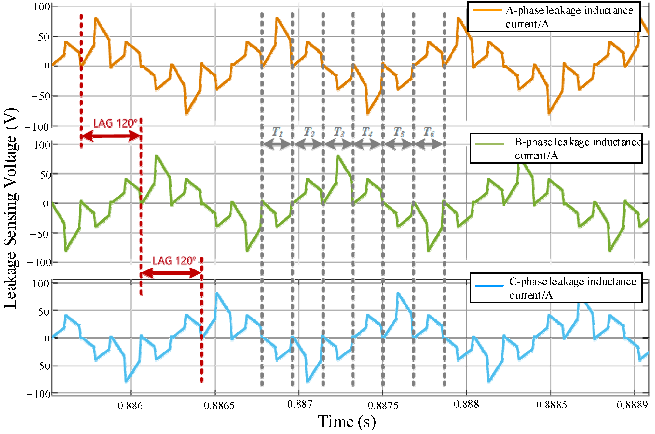
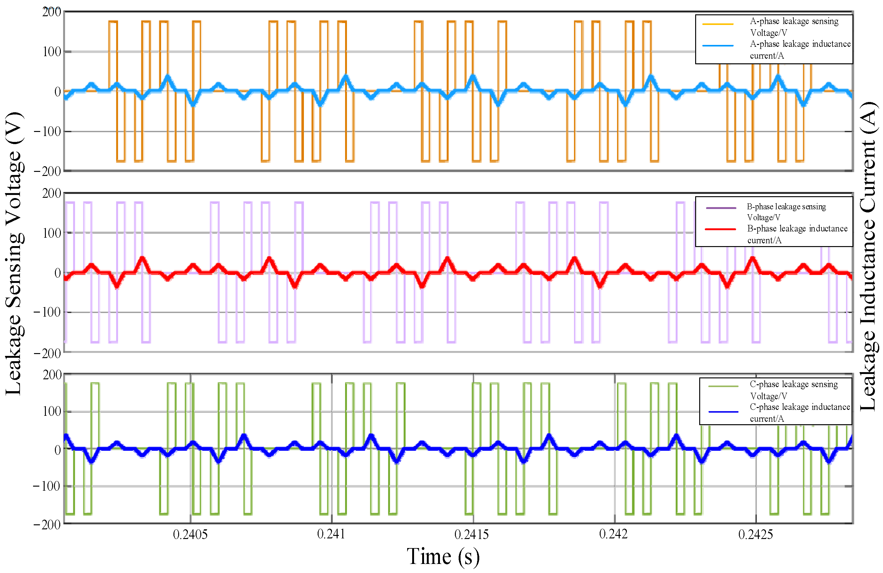
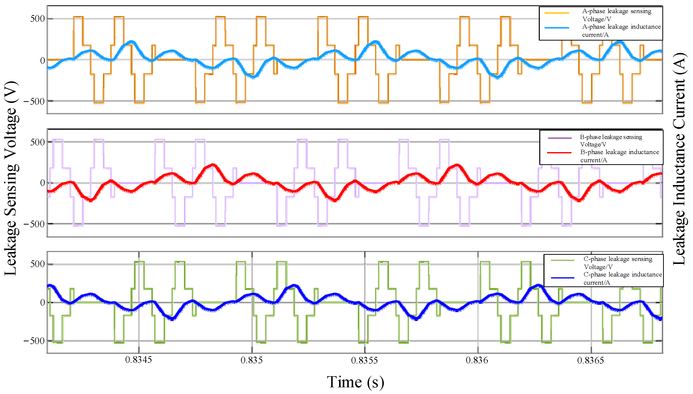
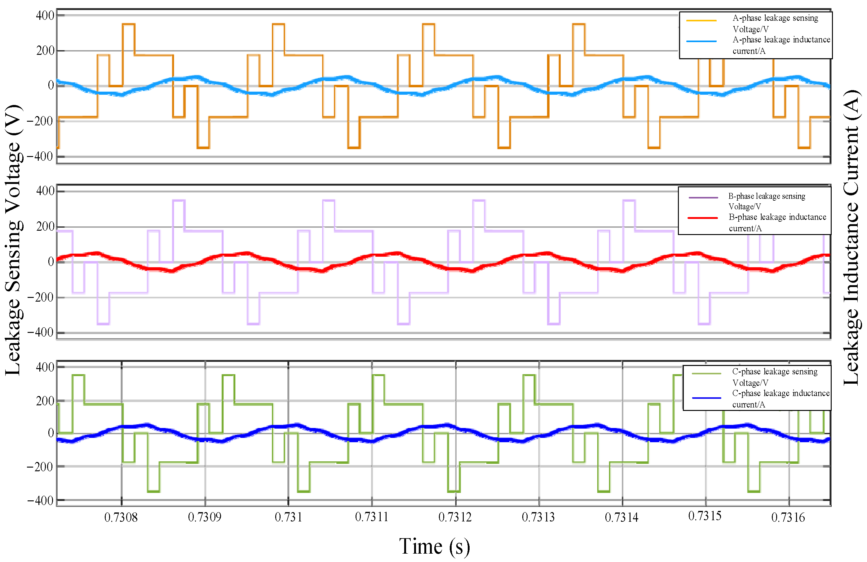
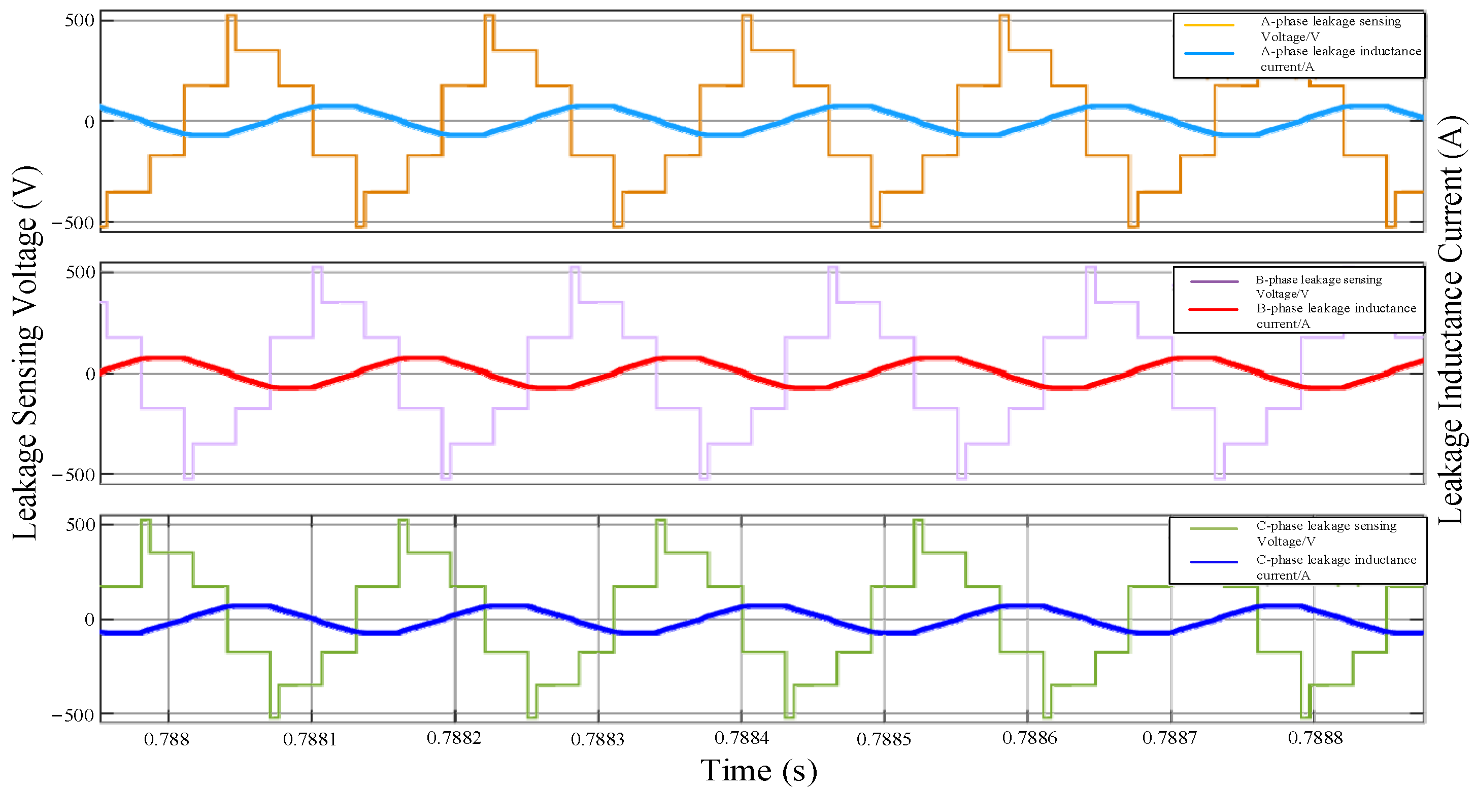
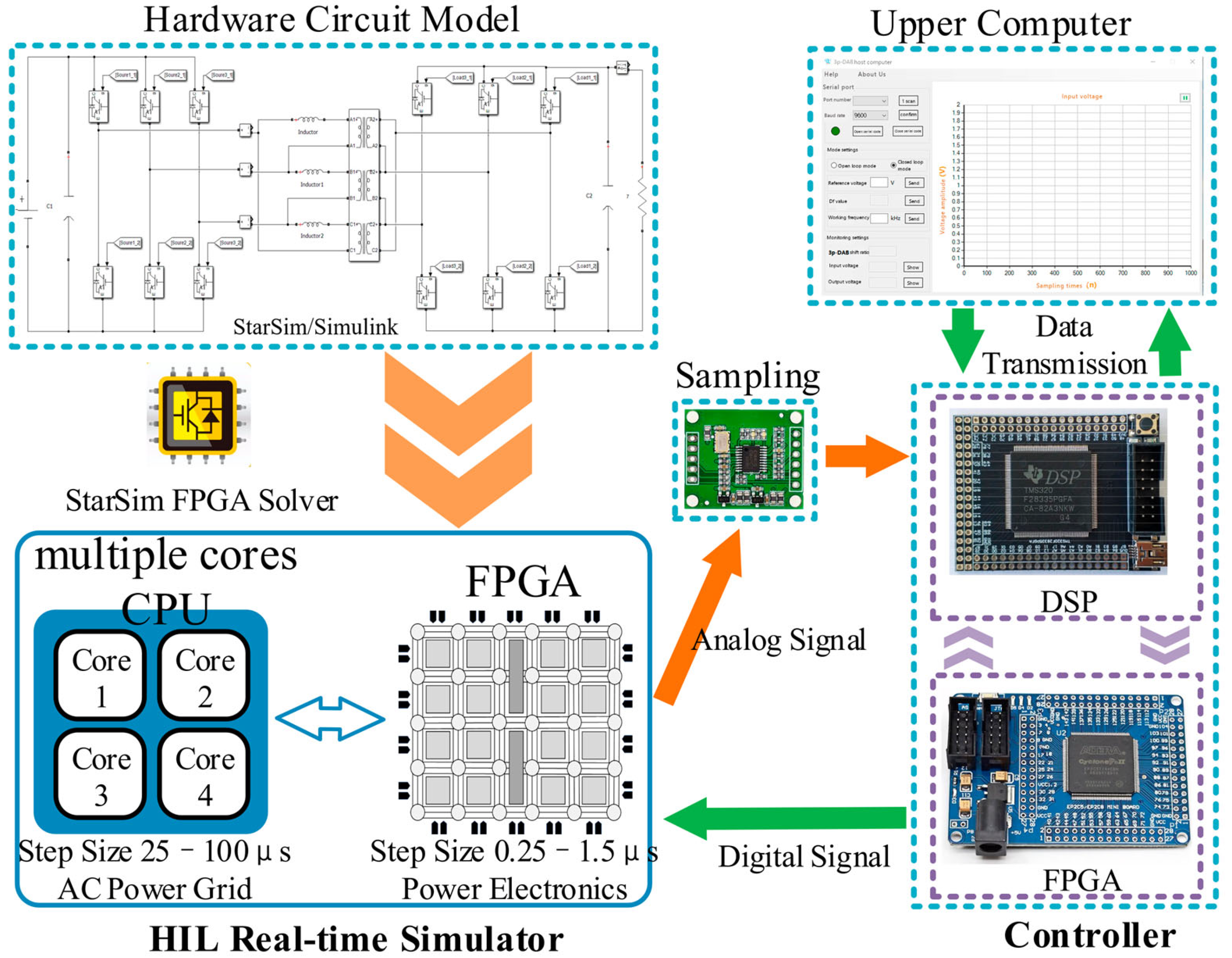
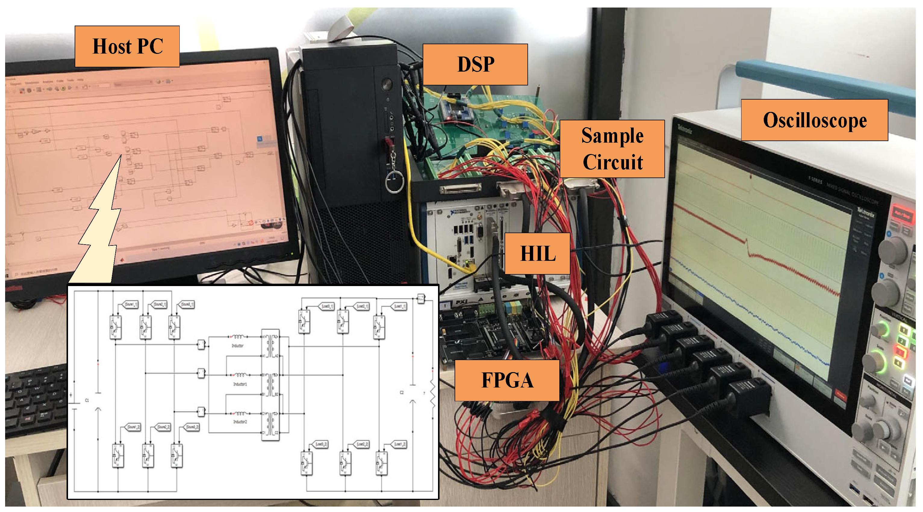
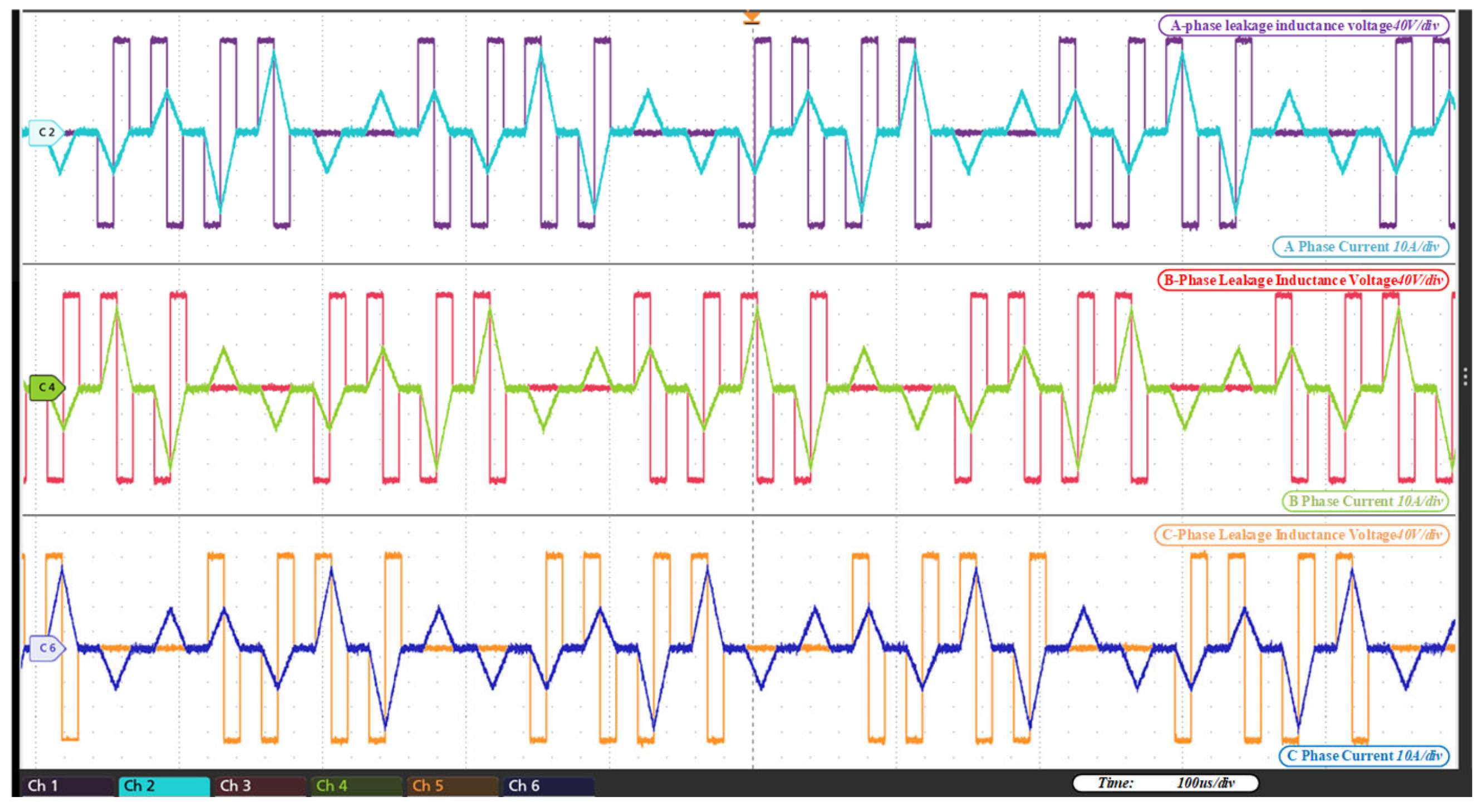
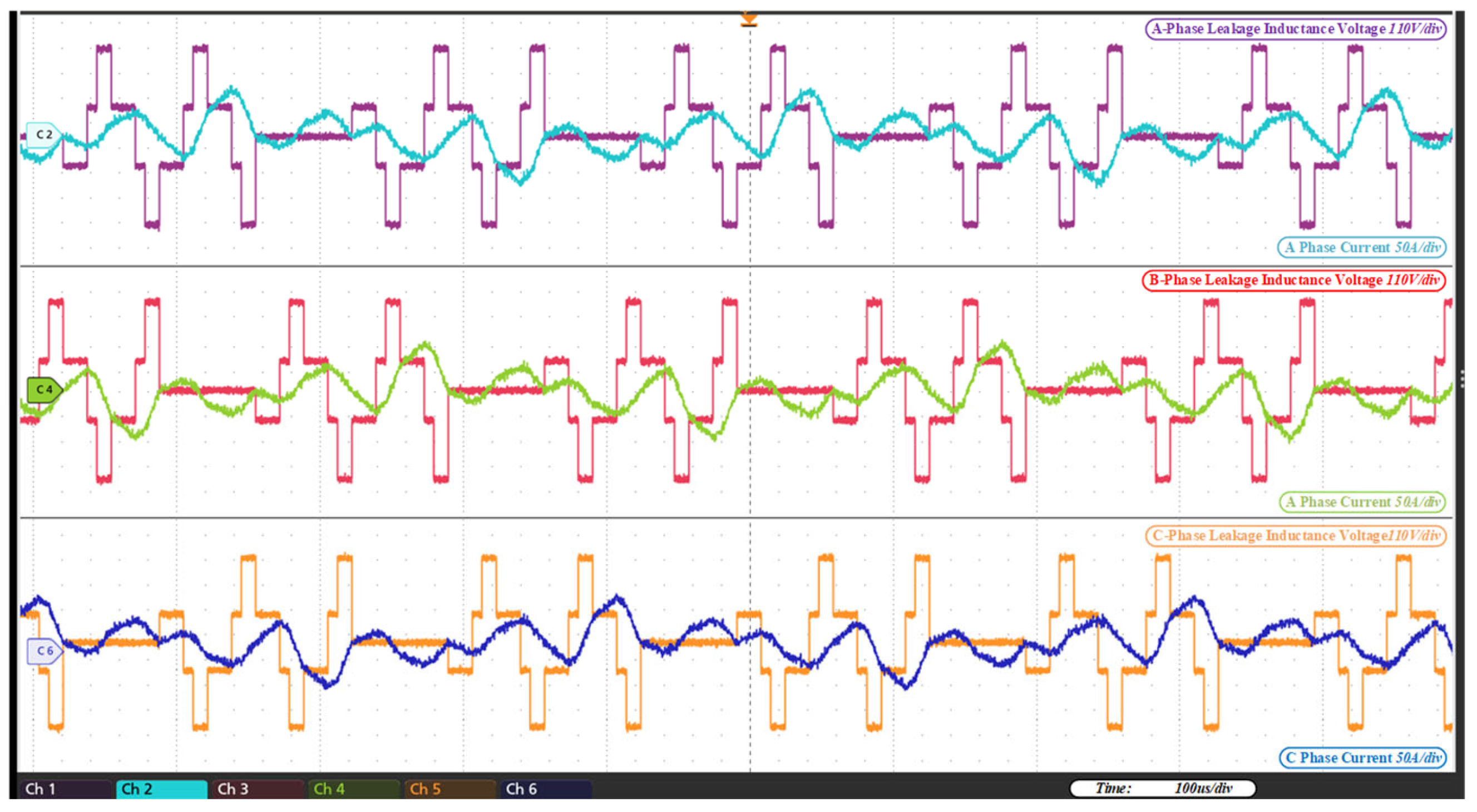
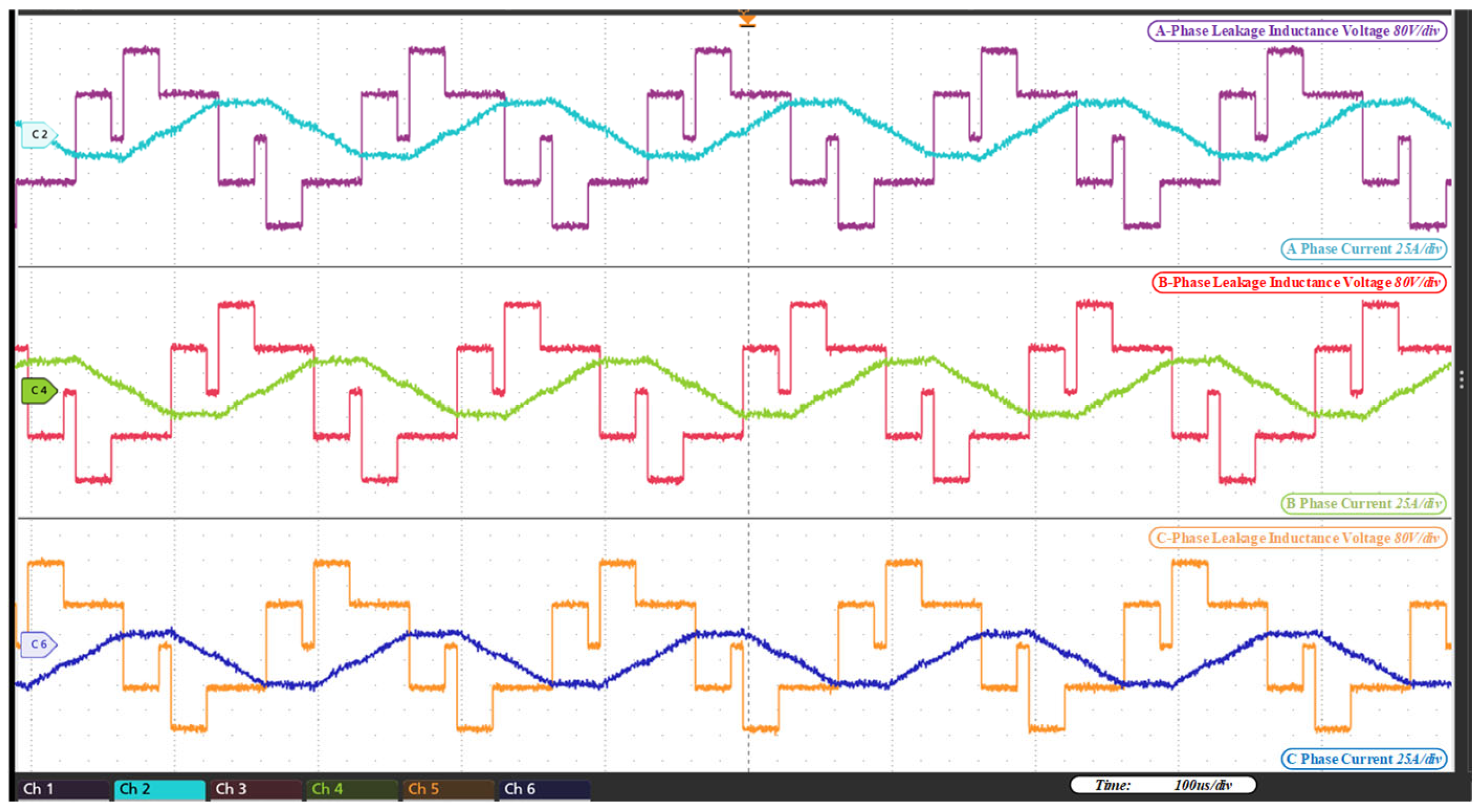
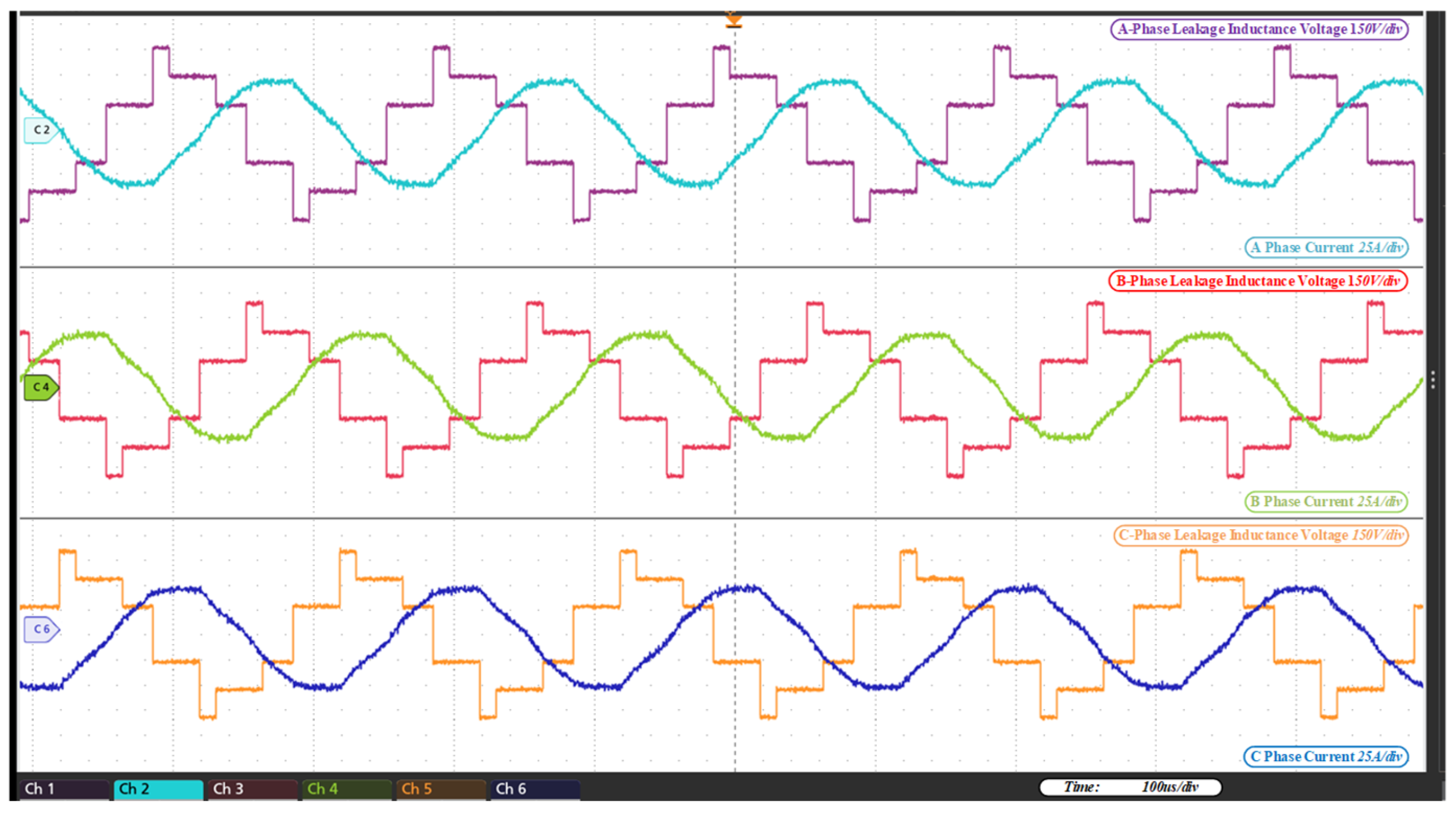
6. Experimental Verification

To demonstrate the practical feasibility of the proposed hybrid control scheme for the 3p-DAB, this section first conducts experimental validation based on a HIL (hardware-in-the-loop) simulation platform. The circuit design requirements and parameters refer to Table 11 and Table 12, while the platform setup is shown in Figure 18, and the specific laboratory hardware platform is illustrated in Figure 19. The experimental focus of this section is to verify the effectiveness of the proposed multimodal switching and optimized operation control. Finally, the experimental results are analyzed in detail.
HIL simulation connects simulated hardware components with real ones, enabling the use of digital models to replace actual system operations. The experimental results obtained through this technique closely resemble those of actual system operations. Moreover, HIL allows for real-time modification of hardware parameters and monitoring, which helps improve the development efficiency of control algorithms. It has been widely used in the development and design verification of circuits [26]. Considering circuit design costs and control algorithm development efficiency, and based on available laboratory resources, a schematic diagram of the experimental platform based on StarSim HIL (ModelingTech Energy Technology Co., Ltd., Nanjing, China) is shown in Figure 18.
The HIL experimental platform is constructed according to the schematic diagram shown in Figure 19. This platform consists of a simulator running the main circuit model and a combined controller composed of a DSP (TMS320F28335) (Texas Instruments Inc., Dallas, TX, USA) and an FPGA (EP4CE10F17C8N) (Intel Corporation (formerly Altera), San Jose, CA, USA). The host configuration parameters are transmitted via the simulator to the sampling circuit, where they are filtered. The DSP then executes the control algorithm, while the FPGA simultaneously performs optimized scheme table lookup, storage, and modulation wave generation. Finally, the drive signals are fed back to the simulator to form a closed loop, and an oscilloscope monitors waveform dynamics in real time.
Next, we conduct a detailed analysis of the experimental results under four operating conditions:
(1)
Operating performance of the 3 p S P C P S _ t r i mode under Power1 condition:
In this scenario, the open-loop controlled hardware circuit is set with parameters D f = 0.15 and d = 0.5 , corresponding to the Power1 operating condition. As shown in Figure 20, the experimental waveforms of the three-phase currents and the voltages at the leakage inductance ends are presented. According to the analysis in Section 3.2, the circuit is expected to operate in the 3 p S P C P S _ t r i mode. The experimental results show that the three-phase current waveforms exhibit a triangular shape, and the relationship among the three-phase currents aligns with the analysis of the 3pSPCPS mode. The experimental results are very close to the simulation results shown in Figure 14.
(2)
Operating performance of the 3 p S P C P S _ t r a p e mode under the Power2 condition:
In this scenario, the open-loop controlled hardware circuit is configured with parameters D f = 0.40 and d = 0.5 , corresponding to the P o w e r 2 operating condition. As shown in Figure 21, the experimental waveforms of the three-phase currents and the voltages at the leakage inductance ends are presented. At this point, the circuit is expected to operate in the 3 p S P C P S _ t r a p e mode. The three-phase current waveforms exhibit a trapezoidal shape, and the relationship among the three-phase currents conforms to the analysis of the 3pSPCPS mode. The experimental results are very close to the simulation results shown in Figure 15.
(3)
Operating performance of the 3pSPCPS mode under P o w e r 3 condition:
In this scenario, the open-loop controlled hardware circuit is configured with parameters D f = 0.65 and d = 0.5 , corresponding to the P o w e r 3 operating condition. As shown in Figure 22, the experimental waveforms of the three-phase currents and the voltages at the leakage inductance ends are presented. According to the analysis in Section 3.2, the circuit is expected to operate in the 3pSPCPS mode. The experimental results indicate that the relationship between the three-phase currents conforms to the mode analysis of the conventional SPS control under the condition of 0 D 3 p S P S 1 / 3 . The experimental results closely match the simulation results shown in Figure 16.
(4)
Operating performance of the 3pSPCPS mode under P o w e r 4 condition:
In this scenario, the open-loop controlled hardware circuit is configured with parameters D f = 0.85 and d = 0.5 , corresponding to the Power4 operating condition. As shown in Figure 23, the experimental waveforms of the three-phase currents and the voltages at the leakage inductance ends are presented. According to the analysis in Section 3.2, the circuit is expected to operate in the 3pSPCPS mode. The experimental results show that the relationship among the three-phase currents conforms to the mode analysis under the conventional SPS control with 1 / 3 D 3 p S P S 1 / 2 . The experimental results are very close to the simulation results shown in Figure 17.
As shown above, both the simulation and the experiment have verified the operating characteristics of the proposed control strategy at different power intervals of the 3p-DAB. The two show a high degree of consistency in terms of the output voltage, inductor current waveforms, and the zero-voltage turn-on characteristics under soft-switching conditions. Although there are certain fluctuations and ripples in the experiment, the overall trend is consistent with the simulation analysis, which further verifies the practicality and accuracy of the theoretical model.

7. Conclusions

Firstly, in response to the challenge of achieving soft-switching and targeted optimization under traditional control for the 3p-DAB across a wide voltage range and under medium to low-power conditions, the 3 p S P C P S operating mode was introduced to enable the 3p-DAB to function in a manner similar to the 1p-DAB. Subsequently, a standardized global operational strategy was proposed for various conditions within wide voltage applications. This strategy allows the 3p-DAB to operate in the 3pSPCPS mode under medium to low-power conditions to extend the range of soft-switching and minimize current stress, and in the 3pSPS mode under high-power conditions to increase the power transmission limit. Following that, the operational characteristics of this multimodal switching management scheme were analyzed. This optimized operational control not only preserves the high-power transmission features of the 3p-DAB but also expands the soft-switching range. Finally, through the simulation verification of the 3p-DAB and hardware-in-the-loop simulation, the feasibility of implementing the 3pSPCPS mode and the rationality of the working effects of mode switching under various conditions were demonstrated.
Although the proposed control strategy achieves soft-switching and optimization across wide voltage and power ranges, the current work still has several limitations. First, the analysis is based on idealized component models and assumes a perfectly symmetrical 3-phase DAB topology. Second, the experimental validation is conducted on a fixed-rated 5kW setup, limiting generalization. In future works, the proposed method can be extended to systems with non-idealities such as parasitic capacitance, component mismatches, and thermal variations. Additionally, adaptation to multi-port or modular DAB topologies and implementation on real-time embedded platforms will be pursued to further evaluate the control robustness and practical applicability.

Author Contributions

Validation, R.W.; Data curation, S.J.; Writing—original draft, C.Z.; Writing—review and editing, C.H. All authors have read and agreed to the published version of the manuscript.

Funding

This research received no external funding.

Data Availability Statement

The original contributions presented in this study are included in the article. Further inquiries can be directed to the corresponding author.

Conflicts of Interest

Author Shaoxu Jiang was employed by the State Grid Jibei Electric Power Co., Ltd., Tangshan Power Supply Company. The remaining authors declare that the research was conducted in the absence of any commercial or financial relationships that could be construed as a potential conflict of interest.

Nomenclature

Abbreviations Sets and Indices f Switching frequency
DABDual Active Bridge v c d , v a b Reflected secondary-side voltage, Primary-side voltage between nodes a and b
3p-DABThree-Phase Dual Active Bridge D 1 , D 2 , D 3 Duty ratios
1p-DABSingle-Phase Dual Active Bridge V 1 Input voltage
3pSPCPSThree-Phase Single-Cycle Parallel-Cycle Phase-Shifting L S 1 Series leakage inductance
3pSPSThree-Phase Single-Phase-Shift M o d e Operating mode selection variable
TPSThree-Phase-Shift P 3 p S P S Power under 3-phase Single-Phase-Shift control
SPSSingle-Phase-Shift D 3 p S P S Phase-shift ratio in 3-phase SPS mode
EPSExtended Phase-Shift f ( D 3 ) A function of the normalized duty ratio D 3
APSAsymmetric Phase-Shift 3 p S P S 3-phase Single-Phase-Shift control
DCCDuty Cycle Control i a , i b , i c Phase A, B, C current
RMSRoot Mean SquareDecision Variables
ZVSZero Voltage Switching t 3 Switching time instants within a clock cycle
HILHardware-in-the-Loop D 1 opt On-state duty ratio of switch 1
DSPDigital Signal Processor D 2 opt On-state duty ratio of switch 2
FPGAField Programmable Gate Array D f o p t Optimized virtual phase-shift ratio
Parameters and constants d ^ The reciprocal of the voltage gain
T Switching period v ^ a b , v ^ c d Primary voltage equals the reflected secondary voltage, Reflected secondary voltage equals the primary voltage
D 1 , D 2 Primary and secondary duty ratios D ^ 1 , D ^ 2 , D ^ 3 Mapped duty ratios
3 p S P C P S _ t r i Three-Phase Single-Cycle Parallel-Cycling Phase-Shift Control (Triangular Mode) I b , P b Base current for normalization, Base power for normalization
3 p S P C P S _ t r a p e Three-Phase Single-Cycle Parallel-Cycling Phase-Shift Control (Trapezoidal Mode) D f Virtual phase-shift ratio (used for mode switching and global unification)
P o n Power delivered during switch-on interval P M _ 1 p-DAB Maximum power of 1-phase DAB in mode M
d Voltage gain D b o u n d a r y _ 3 p S P S Boundary duty ratio for switching from 3pSPCPS to 3pSPS
Power1, Power2,
Power3 and Power4
Low-power region, Medium-power region, Quasi-high-power region, High-power region P b o u n d a r y _ h i g h p o w e r int e r m e d i a t e s t a t e Power at the boundary of high-power intermediate state
P b o u n d a r y _ h i g h p o w e r int e r m e d i a t e s t a t e

References

  1. Energy Crisis vs. Energy Revolution; World Knowledge Ltd.: Slough, UK, 2021; Volume 23, pp. 12–13.
  2. Liu, F. International Energy Agency: Global Electricity Demand Will Accelerate. Oil Gas New Energy 2023, 35, 31. [Google Scholar]
  3. Zhao, H. New Challenges in Energy Security During the International Energy Transition. Natl. Secur. Res. 2022, 6, 88–104. [Google Scholar]
  4. Jiang, R. The Global Economic Impact of the Energy Crisis. World Knowl. 2022, 21, 72–73. [Google Scholar]
  5. Saranyaa, J.S.; Peer, F.A. A Comprehensive Survey on the Current Trends in Improvising the Renewable Energy Incorporated Global Power System Market. IEEE Access 2023, 11, 24016–24038. [Google Scholar] [CrossRef]
  6. Wang, R.; Ma, D.; Li, M.-J.; Sun, Q.; Zhang, H.; Wang, P. Accurate Current Sharing and Voltage Regulation in Hybrid Wind/Solar Systems: An Adaptive Dynamic Programming Approach. IEEE Trans. Consum. Electron. 2022, 68, 261–272. [Google Scholar] [CrossRef]
  7. International Energy Agency. The Worst Global Energy Crisis May Still Be Ahead. China Foreign Energy 2022, 27, 103. [Google Scholar]
  8. Wang, R.; Hu, J.; Sun, Q.; Zhang, H.; Wang, P. Electric Vehicle-Research on Energy Reciprocity Control Strategy. Sci. China Technol. Sci. 2022, 52, 957–970. [Google Scholar]
  9. Wang, R.; Li, M.J.; Wang, Y.; Sun, Q.; Zhang, P. A Study of Novel Real-Time Power Balance Strategy with Virtual Asynchronous Machine Control for Regional Integrated Electric-Thermal Energy Systems. Sci. China Technol. Sci. 2024, 67, 2074–2089. [Google Scholar] [CrossRef]
  10. Zhai, S.; Zhang, Z.; Wang, W.; Li, X.; Chen, Y. Research on Energy Mutual Aid Control Strategy for Electric Vehicles. Integr. Smart Energy 2025, 2025, 1–9. [Google Scholar]
  11. Wang, R.; Yu, X.; Sun, Q.; Li, D.; Gui, Y.; Wang, P. The Integrated Reference Region Analysis for Parallel DFIGs’ Interfacing Inductors. IEEE Trans. Power Electron. 2024, 39, 7632–7642. [Google Scholar] [CrossRef]
  12. Wang, R.; Sun, Q.; Hu, W.; Li, Y.; Ma, D.; Wang, P. SoC-Based Droop Coefficients Stability Region Analysis of the Battery for Stand-Alone Supply Systems with Constant Power Loads. IEEE Trans. Power Electron. 2021, 36, 7866–7879. [Google Scholar] [CrossRef]
  13. Wang, R.; Sun, Q.; Zhang, P.; Gui, Y.; Qin, D.; Wang, P. Reduced-Order Transfer Function Model of the Droop-Controlled Inverter via Jordan Continued-Fraction Expansion. IEEE Trans. Energy Convers. 2020, 35, 1585–1595. [Google Scholar]
  14. Wang, Q.; Zhang, Z.; Liu, B.; Han, D.; Zhao, M.; Guo, J.; Li, S.; Guo, Y. Global Optimization Control of Minimum Reflux Power for Dual Active Bridge Converters Under Dual Phase Shift Control. Power Syst. Technol. 2024, 48, 3921–3930. [Google Scholar]
  15. Yang, X.; Wang, J.; Kong, L.; Du, Y.; Zhang, T. Efficiency Optimization Method for Dual Active Bridge Converters Under Voltage Mismatch Operating Conditions. Trans. China Electrotech. Soc. 2022, 37, 6239–6251. [Google Scholar]
  16. Zeng, J.; Zhang, C.; Cao, B.; Yu, X.; Lan, Z.; Zou, B.; Wang, T.; Cao, Y. Fundamental Circulating Current Optimization Control Strategy for Dual Active Bridge DC-DC Converter Based on Unified Phase-Shifting Control Model. Electr. Power Autom. Equip. 2024, 44, 74–81. [Google Scholar]
  17. Sun, J.; Qiu, L.; Liu, X.; Ma, J.; Rodriguez, J.; Fang, Y. Model-Free Moving-Discretized-Control-Set Predictive Control for Three-Phase Dual-Active-Bridge Converters. IEEE Trans. Power Electron. 2024, 39, 9160–9173. [Google Scholar] [CrossRef]
  18. Schulz, G.; Bauman, J. Time-Domain Analysis and Optimization of a Three-Phase Dual-Active-Bridge Converter with Variable Duty-Cycle Modulation. IEEE Trans. Power Electron. 2023, 38, 500–510. [Google Scholar] [CrossRef]
  19. Chen, H.; Ouyang, S.; Liu, J.; Li, X. An Asymmetrical Phase-Shift Scheme of Three-Phase Dual Active Bridge with Minimum Current Root-Mean-Square Value Control. IEEE Trans. Power Electron. 2022, 37, 6320–6333. [Google Scholar] [CrossRef]
  20. Van Hoek, H.; Neubert, M.; De Doncker, R.W. Enhanced Modulation Strategy for a Three-Phase Dual Active Bridge-Boosting Efficiency of an Electric Vehicle Converter. IEEE Trans. Power Electron. 2013, 28, 5499–5507. [Google Scholar] [CrossRef]
  21. Tu, C.; Guan, L.; Xiao, F.; Liu, B.; Ge, Q.; Lan, Z. Modal Analysis Method for Dual Active Bridge DC-DC Converters. Proc. CSEE 2019, 39, 5468–5479. [Google Scholar]
  22. Gong, L.; Li, W.; Xu, J.; Li, H.; Wang, Y. Hybrid Multi-Phase Shifting Control Strategy for High-Frequency DAB Converters Based on Multi-Objective Optimization. Proc. CSEE 2024, 44, 1517–1534. [Google Scholar]
  23. Sun, B.; Li, J.; Zhang, Q.; Yang, Z.; Deng, X. Dual Phase-Shifted Segmented Control of Minimum Reflux Power for Bidirectional Full-Bridge DC-DC Converter Based on ZVS. Acta Energiae Solaris Sin. 2023, 44, 39–48. [Google Scholar]
  24. Ren, Q.; Ai, S. DAB Three Degree of Freedom Optimization Control Strategy for the Entire Operating Range. Chin. J. Electr. Eng. 2020, 40, 2500–2510. [Google Scholar]
  25. Yu, H.; Hang, L.; Zhang, X.; He, Z.; He, Y.; Shen, L. Globally Unified ZVS and Quasi-Optimal Minimum Conduction Loss Modulation of DAB Converters. IEEE Trans. Transp. Electrif. 2022, 8, 3989–4000. [Google Scholar] [CrossRef]
  26. Wang, R.; Jiang, S.; Ma, D.; Sun, Q.; Zhang, H.; Wang, P. The Energy Management of Multiport Energy Router in Smart Home. IEEE Trans. Consum. Electron. 2022, 68, 344–353. [Google Scholar] [CrossRef]
Figure 1. Topology diagram of 1p-DAB and 3p-DAB.
Processes 13 01921 g001
Figure 2. 3p-DAB parallel-phase operation diagram.
Processes 13 01921 g002
Figure 3. Operating status of switch tube at P ower 1 and T 2 .
Processes 13 01921 g003
Figure 5. Switch current waveform of a circuit under two working conditions of P ower 1 and Power 2 .
Processes 13 01921 g005
Figure 6. Hysteresis control scheme.
Processes 13 01921 g006
Figure 7. Multi-mode control strategy with power range partitioning under wide voltage conditions.
Processes 13 01921 g007
Figure 8. Global power range of a soft-switching area diagram with wide voltage range.
Processes 13 01921 g008
Figure 9. Simulation model of 3p-DAB operation management control based on Simulink.
Processes 13 01921 g009
Figure 10. 3p-DAB output results in the 3pSPCPS operating mode.
Processes 13 01921 g010
Figure 11. Simulation of switching tube drive signal control under 3pSPCPS.
Processes 13 01921 g011
Figure 12. Voltage and leakage current at both ends of the three-phase leakage inductance.
Processes 13 01921 g012
Figure 13. Simulation results of three-phase leakage current.
Processes 13 01921 g013
Figure 14. Circuit operation of the 3 p S P C P S _ t r i operating mode under the Power1 working condition.
Processes 13 01921 g014
Figure 15. Circuit operation of the 3 p S P C P S _ t r a p e operating mode under the Power2 working condition.
Processes 13 01921 g015
Figure 16. Circuit operation of the 3pSPS operating mode under the Power3 working condition.
Processes 13 01921 g016
Figure 17. Circuit operation of the 3pSPS operating mode under the Power4 working condition.
Processes 13 01921 g017
Figure 18. Schematic diagram of a HIL-based experiment.
Processes 13 01921 g018
Figure 19. Experimental platform.
Processes 13 01921 g019
Figure 20. Experimental results of three-phase current and leakage inductance terminal voltage under the Power1 working condition.
Processes 13 01921 g020
Figure 21. Experimental results of three-phase current and leakage inductance terminal voltage under the Power2 working condition.
Processes 13 01921 g021
Figure 22. Experimental results of three-phase current and leakage inductance terminal voltage under the P o w e r 3 working condition.
Processes 13 01921 g022
Figure 23. Experimental results of three-phase current and leakage inductance terminal voltage under the P o w e r 4 working condition.
Processes 13 01921 g023
Table 1. Comparison of advantages and disadvantages of three feasible schemes of 3p-DAB and 1p-DAB.
Non-CyclicFixed CycleSingle Cycle
Single phaseAdvantages: Simple implementation, high reliability
Disadvantages: Circuit redundancy
Advantages: Higher reliability
Disadvantages: Inefficient circuit utilization
Advantages: Higher reliability
Disadvantages: Inefficient circuit utilization
Parallel phaseAdvantages: Efficient circuit utilization
Disadvantages: Uneven heating, high requirements for parallel symmetry
Advantages: Efficient circuit utilization, uniform heating
Disadvantages: Control requires additional costs, fluctuations in the cycling process, high requirements for parallel symmetry
Advantages: High circuit utilization, uniform heating, low thermal design difficulty
Disadvantages: High requirements for parallel symmetry
Table 2. Table of switching status and switching sequence.
T1T2T3T4T5T6T7
PWM1SASA, SBSBSB, SCSCSC, SASA
PWM2SB, SCSCSC, SASASA, SBSBSB, SC
Table 3. Optimal buck scheme for forward power transmission at medium and low power.
ConditionPower RangeOperating ModeOptimization
P o w e r 1 0 , ( 1 d ) d 2 π 2 3 p S P C P S _ t r i D 1 opt = 2 P o n ( 1 d ) π , D 2 opt = 1 d 2 P o n ( 1 d ) π , D f o p t = 2 ( 1 d ) π P o n 2 d π
P o w e r 2   ( 1 d ) d 2 π 2 , d π 4 3 p S P C P S _ t r a p e D 1 opt = 1 ( 1 d ) d π 4 P o n 1 2 d + 2 d 2 d π , D 2 opt = 1 , D f o p t = 1 2 1 2 d d π 4 P o n 1 2 d + 2 d 2 π
Table 4. Boost optimization scheme for forward power transmission at medium and low power.
ConditionPower RangeOperating ModeOptimization
P o w e r 1 0 , ( d 1 ) π 2 d 3 3 p S P C P S _ t r i D 1 opt = 2 d P o n ( d 1 ) π , D 2 opt = d 2 d P o n ( d 1 ) π , D f o p t = d 2 ( 1 1 / d ) π P o n 2 π
P o w e r 2   ( d 1 ) π 2 d 3 , π 4 d 3 p S P C P S _ t r a p e D 1 opt = 1 d π 4 d 2 P o n ( d 1 ) π , D 2 opt = 1 , D f o p t = 1 2 1 2 1 / d π / d 4 P o n ( 1 1 / d ) 2 π
Table 5. Optimal control scheme of wide voltage in forward medium and low transmission power.
Voltage GainConditionPower RangeOperating ModeOptimization
d < 1 P o w e r 1 0 , d 2 ( 1 d ) 2 3 p S P C P S _ t r i D 1 = 2 d P n 1 d D 2 = D 1 d , D 3 = 0
P o w e r 2 d 2 ( 1 d ) 2 , d 4 3 p S P C P S _ t r a p e D 1 = 1 ( 1 d ) 1 4 P n 1 2 d + 2 d 2 D 2 = 1 , D 3 = D 1 d 2 ( 1 d )
d 1 P o w e r 1 0 , d 1 2 d 3 3 p S P C P S _ t r i D 2 = 2 P n d 1 D 1 = d D 2 , D 3 = d D 2 D 2
P o w e r 2 d 1 2 d 3 , 1 4 d 3 p S P C P S _ t r a p e D 2 = 1 ( d 1 ) 1 4 P n d 2 2 d + 2 D 1 = 1 , D 3 = ( 2 d ) D 2 + 2 d 3 2 ( d 1 )
Table 6. Lower control table of forward high transmission power.
Power RangeOperating ModeOptimization Strategy
0 , d 2 3 p S P S D 3 p S P S = 2 3 1 3 4 6 P n d
d 2 , 7 d 12 3 p S P S D 3 p S P S = 1 2 1 2 7 9 4 P n 3 d
Table 7. Corrected low and medium power range table.
Voltage Gain P o w e r 1 P o w e r 2
d < 1 0 , d 2 ( 1 d ) 3 d 2 ( 1 d ) 3 , d 6
d 1 0 , d 1 3 d 3 d 1 3 d 3 , 1 6 d
Table 8. Working condition division table of full power range.
Condition P o w e r 1
(Low Power)
P o w e r 2
(Medium Power)
P o w e r 3
(Quasi-High Power)
P o w e r 4
(High Power)
D f range [ 0 , 1 d 2 ] ( 1 d 2 , 1 2 ] ( 1 2 , 0.5 + 10 2 2 ( 10 1 ) ] ( 0.5 + 10 2 2 ( 10 1 ) , 1 ]
Operating mode 3 p S P C P S _ t r i 3 p S P C P S _ t r a p e 3 p S P S
Optimization D 1 = 2 d 1 d D f , D 2 = 2 1 d D f D 1 = 1 ( 1 d ) 1 2 D f d D 2 = 1 D 3 p S P S = D f 0.5 0.5 D b o u n d a r y _ 3 p S P S 0.5 + D b o u n d a r y _ 3 p S P S
Table 9. Wide voltage global unified optimal control scheme under forward transmission power.
Voltage Gain D f RangeConditionControl ModeOperation Plan
d < 0.95 [ 0 , 1 d 2 ] P o w e r 1 3 p S P C P S _ t r i D 1 = 2 d 1 d D f , D 2 = 2 1 d D f
( 1 d 2 , 0.45 ] P o w e r 2 3 p S P C P S _ t r a p e D 1 = 1 ( 1 d ) 1 2 D f d D 2 = 1
( 0.45 , 0.5 ] hysteresis zone
( 1 2 , 2 10 3 2 ( 10 1 ) ] P o w e r 3 3 p S P S D 3 p S P S = D f 0.5 0.5 D b o u n d a r y _ 3 p S P S 0.5                                                             + D b o u n d a r y _ 3 p S P S
( 2 10 3 2 ( 10 1 ) , 1 ] P o w e r 4
d [ 0.95 , 1.05 ] ( 0 , 0.45 ] medium and low power level 1 p S P S D 1 = 1 , D 2 = 1
( 0.45 , 0.5 ] hysteresis zone
( 1 2 , 2 10 3 2 ( 10 1 ) ] P o w e r 3 3 p S P S D 3 p S P S = D f 0.5 0.5 D b o u n d a r y _ 3 p S P S 0.5                                                             + D b o u n d a r y _ 3 p S P S
( 2 10 3 2 ( 10 1 ) , 1 ] P o w e r 4
d > 1.05 0 , d 1 2 d P o w e r 1 3 p S P C P S _ t r i D 1 = 2 d d 1 D f D 2 = 2 d 1 D f
d 1 2 d , 0.45 P o w e r 2 3 p S P C P S _ t r a p e D 1 = 1 D 2 = 2 d + 2 ( d 1 ) D f
( 0.45 , 0.5 ] hysteresis zone
( 1 2 , 2 10 3 2 ( 10 1 ) ] P o w e r 3 3 p S P S D 3 p S P S = D f 0.5 0.5 D b o u n d a r y _ 3 p S P S 0.5                                                             + D b o u n d a r y _ 3 p S P S
( 2 10 3 2 ( 10 1 ) , 1 ] P o w e r 4
Table 10. Simulation model system parameter table.
ParametersNumerical Value
Input voltage U350 V
Input capacitor C12200 μF
Output capacitor C22200 μF
High-frequency transformer ration1.1
3p-DAB leakage inductance La/Lb/Lc0.25 mH
Switching frequency fs5.6 kHz
Table 11. Electrical parameter design requirements.
Technical IndicatorsParametersTechnical IndicatorsParameters
System Rated Power:5 kWSwitching Frequency:10 kHz
Maximum Transmission Power:10 kWInput Voltage:300 V
Input Voltage Overshoot:<10%Output Voltage:150 V–400 V
Input Voltage Droop:<10%Output Voltage Ripple Ratio:<5%
Table 12. Circuit design parameters.
Electrical ParametersParameters
Switching frequency:10 kHz
Number of MOSFETs:12
Input capacitor C1:1000 µF
Input capacitor C2:1500 µF
Leakage inductance L:140 µH
Disclaimer/Publisher’s Note: The statements, opinions and data contained in all publications are solely those of the individual author(s) and contributor(s) and not of MDPI and/or the editor(s). MDPI and/or the editor(s) disclaim responsibility for any injury to people or property resulting from any ideas, methods, instructions or products referred to in the content.

