Abstract
In two-dimensional (2D) materials research, exfoliating 2D transition metal dichalcogenides (TMDs) from their growth substrates for device fabrication remains a significant challenge. Current methods, such as those involving polymers, metals, or chemical etchants, suffer from limitations like contamination, defect introduction, and a lack of scalability. Here, we demonstrate a selenium capping-based exfoliation technique. Its advantage lies in its ability to enable the clean, contamination-free exfoliation and transfer of TMD films. We successfully exfoliated and transferred monolayer and multilayer TMD films, including WSe2 and MoSe2. The selenium capping layer not only enables seamless exfoliation but also protects the film from oxidation, as confirmed by X-ray photoelectron spectroscopy and Raman spectroscopy. This approach is versatile and applicable to a range of TMDs and thicknesses, paving the way for the high-quality, scalable integration of 2D materials into nanoelectronic devices.
1. Introduction
Since the discovery of graphene, the library of two-dimensional (2D) materials has continued to expand rapidly, offering diverse functionalities and properties [1,2,3,4,5,6,7,8,9,10,11]. Among these, transition metal dichalcogenides (TMDs) have gained significant attention due to their atomic-scale thickness, tunable bandgap, and unique proximity effects [12,13,14,15,16,17,18,19,20,21]. TMDs with a direct bandgap in the monolayer limit or those exhibiting spin/valley polarization are particularly promising for applications in optoelectronics and spintronics [22,23,24,25]. Furthermore, the weak van der Waals (vdW) forces between monolayers allow for the stacking of exfoliated films at desired twist angles, enabling the exploration of perfect light absorption and superconductivity [26,27,28,29,30].
Despite these exciting opportunities, research on these materials still heavily relies on the traditional method of the tape exfoliation of bulk crystals [31,32,33,34]. While simple, this method suffers from several limitations, including small flake sizes, low yield, and contamination from adhesive residues, which often require prolonged solvent or plasma treatments [35,36,37,38,39]. Most importantly, tape exfoliation is not scalable, posing a significant bottleneck for the development of large-area devices.
To address these limitations, thin film deposition techniques such as molecular beam epitaxy (MBE) and chemical vapor deposition (CVD) have emerged as promising alternatives for producing large-area 2D films [40,41,42,43]. MBE, in particular, offers several advantages, including exceptional film quality, wafer-scale uniformity, and low defect density. Its low growth temperature makes it compatible with a wide range of commercial substrates, supporting emerging applications like monolithic 3D integration (M3D) for next-generation logic and memory devices. Additionally, MBE is well suited for directly growing heterostructures and superlattices. However, the strong interactions between as-grown films and the growth substrate often prevent their mechanical exfoliation, complicating the transfer process required for further characterization and device fabrication.
Current wafer-scale film transfer techniques involve the use of polymer layers, such as polymethyl methacrylate (PMMA) or polydimethylsiloxane (PDMS), metal layers, or chemical etchants [44,45,46,47,48,49,50,51,52,53,54,55,56,57]. These methods, while effective to some extent, bring the 2D films into direct contact with external agents, raising concerns about contamination, oxidation, unintentional doping, and potential degradation [58,59,60,61,62,63]. See Table 1 for a comparison.

Table 1.
Comparison of different exfoliation methods regarding defect density, yield, contamination levels, advantages, and disadvantages.
In this work, we demonstrate a novel approach to addressing these challenges by capping TMD films with selenium. This capping layer enables the efficient exfoliation of TMD layers, taking advantage of the interaction between selenium and the transition metal selenide interface. Additionally, since these TMDs are selenides, the Se capping layer ensures the ultra-clean transfer of the TMD layers without the introduction of new elements. Unlike conventional methods, our process avoids the use of polymers, metal layers, or chemical etchants, preserving the purity and quality of the films. Additionally, the selenium capping layer protects the films from oxidation during the transfer process. The transferred films maintain their quality, as confirmed by X-ray photoelectron spectroscopy (XPS), Raman spectroscopy, and diffraction. This method is highly versatile, compatible with a wide range of TMD materials and thicknesses, and paves the way for scalable, high-quality 2D material integration in advanced nanoelectronic applications.
2. Materials and Methods
Sample growth in this study was performed in a ScientaOmicron (Uppsala, Sweden) MBE system. MBE operates in an ultrahigh vacuum environment of 10−10 mbar, effectively minimizing background gas molecules that could introduce contamination or alter the deposition trajectory of evaporated atoms. WSe2 growth was performed on a single-side polished c-plane (0001) sapphire wafer through a co-deposition method, where elemental W and Se were evaporated using an e-beam evaporator for W and a valved effusion cell with a cracker for Se. A substrate temperature of 600 °C was used. A constant Se-to-W flux ratio of 200:1 was maintained, as calibrated by the beam flux monitor within the MBE chamber. A W flux of approximately 5 × 10⁻⁹ mbar was achieved with e-beam settings of 200 mA and 6 kV. A Se flux of approximately 1 × 10⁻⁶ mbar was used by setting the Se effusion cell’s reservoir temperature to 130 °C and the cracker tip to 1100 °C. Before initiating the growth, the source shutters were left open for 30 min to stabilize the fluxes. Subsequently, the substrate shutter was opened to expose the substrate to the evaporated source materials, initiating the growth. MoSe2 growth was performed on a double-side polished c-plane sapphire wafer at a growth temperature of 500 °C and a Se-to-Mo ratio of 200:1. A Mo flux of approximately 5 × 10⁻⁹ mbar was used, which was achieved with e-beam settings of 100 mA and 6 kV.
For selenium layer deposition, the substrate temperature was kept at 20 °C, and the sample was exposed to a pure selenium flux of approximately 5 × 10⁻⁶ mbar, evaporated using a standard Knudsen cell with a selenium deposition rate measured to be 35 nm/min. For all samples, selenium was deposited for 30 min, resulting in a 1050 nm thick amorphous selenium film.
Exfoliation and transfer were conducted in a Class 10,000 cleanroom to maintain high cleanliness standards. After Se capping, the sample was taken out from the chamber, and a quarter-section of the 2-inch wafer was cut using a diamond scribe pen. A thermal release tape (Revalpha 3195 V, sourced from Semiconductor Equipment Corp., Moorpark, CA, USA) was then applied to the TMD/Se sample. To ensure uniform adhesion, the tape was gently pressed onto the wafer using a cleanroom wipe as an interface between the TMD/Se/tape stack and the operator’s gloved hand. The tape was then carefully peeled off by hand at no specific peeling angle, effectively exfoliating the TMD/Se layer while leaving the sapphire substrate clean. The exfoliated TMD/Se/tape stack was subsequently transferred onto a SiO2/Si substrate by gently pressing it with a cleanroom wipe to ensure proper contact. The sample was then heated at 170 °C for 10 s on a hot plate, enabling the detachment of the thermal release tape and leaving the TMD/Se layer securely on the SiO2/Si substrate. To eliminate any residual tape contaminants, the sample was sequentially immersed in acetone and isopropyl alcohol (IPA) for 5 min each. Following the cleaning process, the sample was loaded into the MBE loading port and pumped down overnight under a vacuum pressure of ~10⁻⁵ mbar to desorb any residual surface adsorbates, such as H2O, O2, and carbon-based contaminants. The sample was then transferred to the MBE deposition chamber, where it was annealed at 250 °C for 1 h. The selenium desorption process was monitored in real time using reflection high-energy electron diffraction (RHEED) to ensure the complete removal of the Se capping layer, leaving a clean TMD film on the SiO2/Si substrate.
A total of eight samples were prepared and tested. The exfoliation success rate was 75% (six out of eight samples). For the successfully exfoliated samples, 100% of the film was successfully peeled from the sapphire substrate, leaving no film behind on the growth substrate. For the remaining two samples, exfoliation did not occur at all, indicating a binary success/failure outcome rather than partial exfoliation. Further experiments are underway to understand the underlying mechanisms.
Raman spectra were acquired at room temperature using a micro-Raman spectrometer, specifically the NRS-5100 model by Jasco (Tokyo, Japan). A 532 nm excitation wavelength with a power of 4.5 mW/um2 was used. The backscattered signal was dispersed using a 1800 g/mm grating. The scans were conducted with an integration time of 10 s, averaged over five integrations. The spectra were calibrated with respect to the Raman peak of silicon at 520.7 cm−1.
XPS spectra were acquired by a Scientia Omicron (Uppsala, Sweden) XPS system with an Argus CU analyzer and using a monochromated Al Kα source (Energy = 1486.7 eV). A takeoff angle of 90° and pass energy of 15 eV were used. The high-resolution spectra were acquired with an energy interval of 0.05 eV and averaged over 15 scans. A charge neutralizer was used to eliminate charging, and spectra were calibrated with respect to the W 4f7/2 peak at a binding energy value of 32.7 eV.
3. Results
We begin our discussion with the exfoliation of monolayer (ML) tungsten diselenide (WSe2). WSe2 growth was performed on a 2-inch sapphire wafer using the parameters described in the Materials and Methods Section. Growth was monitored in real time by in situ reflection high-energy electron diffraction (RHEED), and ML growth was confirmed by the disappearance of the RHEED pattern of the sapphire substrate and the appearance of the WSe2 pattern, as shown in Figure 1a,b, as well as ex situ Raman measurements.
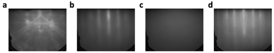
Figure 1.
The RHEED pattern of (a) the c-plane (0001) sapphire wafer, (b) after the growth of WSe2, (c) after the Se capping of WSe2, and (d) after WSe2 recovery post Se desorption. The streaky RHEED pattern in (b) is an indication of crystalline WSe2, while the diffused RHEED pattern in (c) confirms the amorphous nature of the Se capping layer.
After the growth of WSe2, the W and Se sources were turned off, and the substrate temperature was lowered to room temperature (20 °C). The sample was then transferred to the adjacent XPS chamber to collect in situ XPS data on this as-grown WSe2. Subsequently, the sample was returned to the MBE deposition chamber, where it was exposed to a pure selenium flux of approximately 5 × 10⁻⁶ mbar at room temperature. Selenium was deposited for 30 min, which resulted in an approximately 1 μm thick amorphous film of selenium. The amorphous nature of the capping layer was confirmed by the appearance of a diffused RHEED pattern, as shown in Figure 1c. After selenium capping, the sample was taken out of the MBE chamber, and thermal release tape (TRT) was used to exfoliate the Se/WSe2 film stack from the sapphire substrate. Note that, as schematically illustrated in Figure 2, the tape only comes into contact with the top Se cap and not the WSe2 layer.
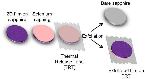
Figure 2.
A schematic illustration of the selenium-assisted exfoliation of a 2D film grown on sapphire, where the film is never brought into direct contact with any metal, polymer, or etchant.
The exfoliated Se/WSe2 film stack was then transferred onto the desired substrate, consisting of 270 nm of thermally grown SiO2 on silicon, and heated at 170 °C on a hot plate for 10 s to release the tape. The Se/WSe2/SiO2 sample was later cleaned with acetone and isopropyl alcohol for 5 min each to remove any tape residue from the surface of the capping layer and then loaded back into the MBE chamber. Lastly, the Se/WSe2/SiO2 stack was annealed at 250 °C for approximately an hour in MBE to desorb the selenium capping layer and recover the transferred WSe2 layer. Se desorption and WSe2 recovery were monitored in real time with RHEED. Figure 1d shows a representative image of the recovered WSe2 film post Se desorption. Finally, the sample was moved to the XPS chamber to collect data on this exfoliated WSe2. Figure 3 shows the film transfer process.
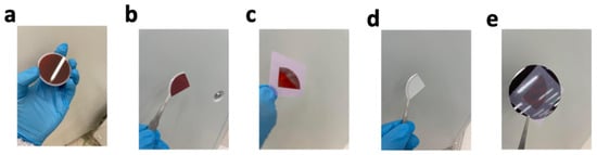
Figure 3.
(a) Selenium-capped WSe2. (b) Small piece used for exfoliation. (c) Se/2D stack exfoliated by thermal release tape. (d) Sapphire substrate post exfoliation. (e) Se/2D stack transferred onto SiO2 substrate.
To confirm whether the exfoliation process worked successfully, we first employed Raman spectroscopy. Figure 4a shows a comparison of the Raman spectra of a monolayer of WSe2 grown on sapphire and later transferred onto a SiO2 substrate. The first thing to note for the as-grown sample is the presence of the degenerate Raman mode E12g/A1g around 250 cm−1 and the 2 LA(M) mode at ~260 cm−1 that are signatures of the semiconducting H-phase of WSe2 [66,67]. The ‘A’ mode refers to an out-of-plane vibrational mode, which involves the movement of atoms perpendicular to the plane of the film, while the ‘E’ mode is an in-plane vibrational mode. These modes are almost degenerate at around 250 cm−1 in monolayer WSe2. The ‘2 LA(M)’ mode is a second-order scattering process which involves longitudinal acoustic phonons at the M point of the Brillouin zone. The absence of the interlayer breathing mode (B2g) around 310 cm−1 confirms the monolayer thickness of the sample, as this mode, caused by interlayer interactions, only appears in multilayer films [68]. Compared with the Raman spectra of the same film transferred onto SiO2, we saw similar Raman peaks with a slight blue shift of ~0.4 cm−1 in the peak position. This small shift, which is likely due to uniaxial strain caused by the SiO2 substrate due to its larger surface roughness (4 Å–8 Å) than sapphire (1 Å–2 Å), has been reported previously [69]. Most importantly, no enhancement was observed in the 2 LA(M) mode of the transferred film which confirms that neither the transfer process nor the cap desorption process introduces any disorder or lattice defects in the transferred film. This observation is significant because an increase in the intensity of the 2 LA(M) mode has been ascribed to be a signature of defective WSe2 films [70].
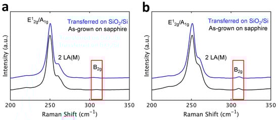
Figure 4.
A Raman comparison of as-grown WSe2 on sapphire (in black) versus the same film transferred on SiO2 (in blue). (a) shows the plot for monolayer WSe2, and (b) shows that for bilayer WSe2. Three measurements were taken for all samples at random locations. Error is ±0.7 cm−1.
To further check whether this method can be used to transfer more than one layer, a bilayer sample of WSe2 was grown and later transferred to SiO2 using the same process. Unlike in monolayer WSe2, the energy degeneracy of the E12g and A1g modes is lifted in bilayer WSe2, resulting in a redshift in the E12g mode and a blueshift in the A1g modes, as reported in Ref. [71]. Consequently, the Raman line shape of bilayer WSe2 appears slightly broader than that of monolayer WSe2, as the bilayer spectrum is now a convolution of two slightly shifted peaks. This is evident in the comparison in Figure 4a,b. This, combined with the observation of the interlayer breathing mode at 310 cm−1 in both the as-grown and transferred bilayer films, confirms that this method is equally effective in exfoliating thicker films.
A significant advantage of this exfoliation technique is that the TMD layer, protected by the selenium capping layer, remains shielded from oxidation. To confirm this, we performed XPS. Figure 5 presents a comparative XPS analysis of an as-grown WSe2 monolayer on the sapphire substrate and the same layer transferred onto SiO2, along with a Se capping layer. The plot includes XPS spectra for the W 4f, W 5p, and Se 3d regions, with the data normalized and aligned relative to the W 4f7/2 peak at 32.7 eV. In the as-grown sample, only the characteristic peaks corresponding to a high-intensity Se–W bond and a low-intensity Se–Se bond are observed, as shown by the peak deconvolution. The presence of Se–Se bonds is similar to that of As–As bonds in the As region of GaAs [72], alongside As–Ga bonds. Oxidized WSe2 typically exhibits additional W–O and Se–O peaks at higher binding energies relative to the main W 4f and Se 3d peaks; however, such peaks were absent in our as-grown film due to the in situ transfer to the XPS chamber [73,74,75]. For the Se capping layer, we observed a single doublet representing the Se–Se bond. The peak position is the same as that of the Se–Se bond in WSe2 but with a broader width, which is attributed to the amorphous structure. The XPS profile of the transferred film closely matched that of the as-grown film, with no W–O or Se–O peaks detected, confirming the oxidation-free nature of the transfer process, even though the capped sample was exposed to air for two days. These findings demonstrate the effectiveness of the transfer method in preventing oxidation, addressing a common challenge associated with alternative transfer techniques.
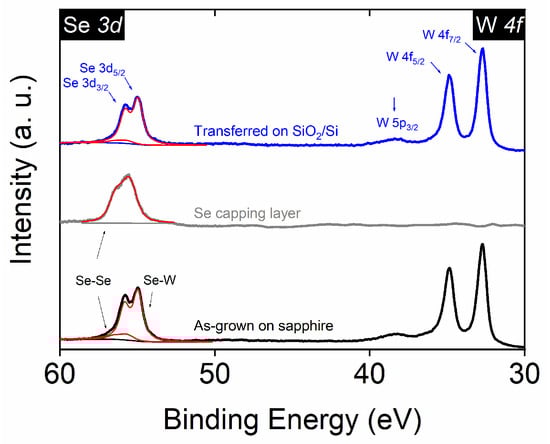
Figure 5.
An XPS comparison of an as-grown WSe2 monolayer and one transferred to SiO2, together with a Se capping layer. The Se regions are fitted in red. For WSe2 samples, two doublets corresponding to Se–W and Se–Se bonds are used, while the Se capping layer is fitted with a single Se–Se doublet. The identical line shapes of WSe2 indicate no oxidation and no residual Se from the cap or any other chemistry changes after film transfer.
Another notable advantage of this transfer method is its versatility, as it is not limited to a specific TMD but can be applied to a wide range of other 2D chalcogenides. For instance, we successfully transferred molybdenum diselenide (MoSe2) as well. Figure 6 presents a Raman analysis comparing a thick MoSe2 film grown on sapphire with the same film after being transferred onto SiO2. The characteristic Raman peaks of MoSe2, corresponding to the A1g and E12g modes, were observed near 242 cm−1 and 287 cm−1, respectively, consistent with the values reported in the literature [76]. Similar to WSe2, few-layer-thick MoSe2 exhibits an interlayer breathing mode near 353 cm−1 [77]. This mode is the strongest for bilayers and gradually diminishes with increasing layer thickness, becoming absent in bulk MoSe2 due to translational symmetry [76]. In our case, we observed a very weak B2g mode, consistent with the target thickness of approximately 5 MLs. Lastly, similar to the results obtained for WSe2, the transferred MoSe2 film exhibited no broadening, peak shifts, or intensity degradation, thereby confirming both the successful transfer and the general applicability of this method.
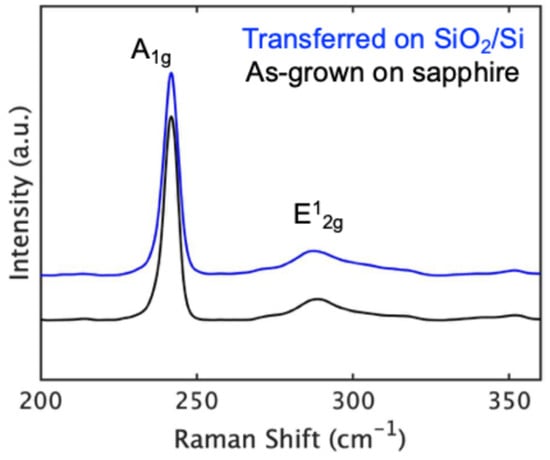
Figure 6.
A Raman comparison of a thick MoSe2 film grown on sapphire (in black) versus the same film transferred on SiO2 (in blue).
Multiple experimental trials showed that the overall peeling efficiency of selenium-assisted exfoliation was 100% and that the entire film, including both monolayers and thick films, was successfully exfoliated from the sapphire growth substrate, leaving no residual material behind. The transfer success rate onto the SiO2/Si target substrate exceeded 95% of the overall film. The minor material loss (~5%) can be avoided through refined handling techniques or automation. The exfoliation and transfer technique proved effective for a wide range of film thicknesses, from monolayers and bilayers to thick films, as demonstrated in Figure 4 and Figure 6.
4. Discussions
The outstanding performance of selenium-assisted exfoliation provides insights into understanding the exfoliation mechanism. Studies on other methods, such as metal-assisted exfoliation, have demonstrated that the stamp layer exhibits higher adhesion energy with 2D materials compared to the substrate. For instance, the average adhesion energy [55] for 2D-2D interactions is 0.45 J/m2, while for 2D sapphire, it is 0.26 J/m2. In contrast, the adhesion energy [55] between nickel and 2D materials reaches 1.4 J/m2. Although the adhesion energy for Se–WSe2 has not yet been reported, considering the Se–W–Se sandwich structure and the bonding of the top Se layer with the selenium capping layer, the van der Waals adhesion is expected to be significantly weaker than that of metal/WSe2 interactions. For example [78], the adhesion energy of Se on graphene has been reported to be only 0.34 J/m2 which is still larger than the 0.26 J/m2 of a TMD film on sapphire, indicating that transfer off the sapphire is still energetically favorable with a Se cap. However, other mechanisms beyond the adhesion energy should also be considered. It has been previously suggested [53] that when a semiconductor comes into contact with a metal or another semiconductor, the built-in electric field exerts a force on both materials, influencing the structure and bonding characteristics, an effect particularly pronounced in 2D materials. Consequently, the interlayer distance between adjacent TMD layers could be altered, in this case, increased, and results in a smaller 2D-2D interaction which facilitates exfoliation [53].
As for the ability of a Se cap to prevent oxidation, selenium is known for its relative inertness to air. Studies have shown that a strong oxidizing agent is required to obtain selenium oxide, and its reaction with oxygen requires catalysts such as nitrogen oxides to facilitate oxidation [79]. Therefore, selenium has been widely used as a capping layer, preventing the thin film from oxidizing [80]. The Se capping layer can be easily evaporated at 200 °C, a low enough temperature to prevent degradation and chalcogen vacancy formation in most TMDs. Here, selenium-assisted exfoliation also benefits from this inert nature in protecting the underlying thin film. These unique physical and chemical properties make selenium a superior candidate for TMD transfer compared to other existing methods.
5. Conclusions
We introduced a selenium-assisted exfoliation technique for the transfer of 2D transition metal dichalcogenide films as a scalable and contamination-free solution to the challenges faced by conventional methods. By employing a selenium capping layer, we demonstrated that monolayer and multilayer TMD films could be efficiently exfoliated and transferred to target substrates while preserving their structural and electronic integrity. Characterization through Raman spectroscopy and X-ray photoelectron spectroscopy confirmed that the transferred films maintained their quality and remained free of defects and oxidation. This versatile approach not only overcomes the limitations of traditional exfoliation methods, such as contamination, oxidation, unintentional doping, damage, and scalability issues, but also offers a platform for integrating various 2D materials into nanoelectronic devices. Moreover, in practical industrial applications, selenium can be deposited using sputtering, e-beam evaporation, or thermal evaporation, offering good uniformity and excellent scalability for large-area applications, an advantage not achievable with polymer- or liquid-assisted methods. We also anticipate this technique to be extendable to other TMDs, such as MoS2 and WS2, with minimal parameter adjustments due to the weak interaction of the Se cap on inert 2D surfaces that enables Se desorption at low temperatures. Additionally, our results suggest a potential strategy for identifying materials suitable as an exfoliation stamp, following the guiding principle that materials with inert properties, shared elemental composition, and low-temperature evaporability are promising candidates. As the demand for wafer-scale, high-quality 2D materials grows, this selenium-assisted exfoliation process presents a significant step forward in advancing the fabrication and application of next-generation electronic and optoelectronic devices.
Author Contributions
R.Y. and C.L.H. conceived and designed this study; R.Y. conducted the experiments and collected data under the guidance of G.Z. and C.L.H. R.Y. and C.L.H. wrote the manuscript with the input from all the authors. All authors have read and agreed to the published version of the manuscript.
Funding
The authors acknowledge funding from SUPREME, one of seven centers in JUMP 2.0, a Semiconductor Research Corporation (SRC) program sponsored by DARPA.
Data Availability Statement
All data that support the findings of this study are included within the article.
Conflicts of Interest
The authors declare no conflicts of interests.
Abbreviations
The following abbreviations are used in this manuscript:
| MBE | Molecular beam epitaxy; |
| MoSe2 | Molybdenum diselenide; |
| RHEED | Reflection high-energy electron diffraction; |
| WSe2 | Tungsten diselenide. |
References
- Novoselov, K.S.; Geim, A.K.; Morozov, S.V.; Jiang, D.; Zhang, Y.; Dubonos, S.V.; Grigorieva, I.V.; Firsov, A.A. Electric Field Effect in Atomically Thin Carbon Films. Science 2004, 306, 666–669. [Google Scholar] [CrossRef] [PubMed]
- Mbayachi, V.B.; Ndayiragije, E.; Sammani, T.; Taj, S.; Mbuta, E.R.; Khan, A.U. Graphene Synthesis, Characterization and Its Applications: A Review. Results Chem. 2021, 3, 100163. [Google Scholar] [CrossRef]
- Lin, Y.-C.; Torsi, R.; Younas, R.; Hinkle, C.L.; Rigosi, A.F.; Hill, H.M.; Zhang, K.; Huang, S.; Shuck, C.E.; Chen, C.; et al. Recent Advances in 2D Material Theory, Synthesis, Properties, and Applications. ACS Nano 2023, 17, 9694–9747. [Google Scholar] [CrossRef]
- Bhimanapati, G.R.; Lin, Z.; Meunier, V.; Jung, Y.; Cha, J.; Das, S.; Xiao, D.; Son, Y.; Strano, M.S.; Cooper, V.R.; et al. Recent Advances in Two-Dimensional Materials beyond Graphene. ACS Nano 2015, 9, 11509–11539. [Google Scholar] [CrossRef]
- Shanmugam, V.; Mensah, R.A.; Babu, K.; Gawusu, S.; Chanda, A.; Tu, Y.; Neisiany, R.E.; Försth, M.; Sas, G.; Das, O. A Review of the Synthesis, Properties, and Applications of 2D Materials. Part. Part. Syst. Charact. 2022, 39, 2200031. [Google Scholar] [CrossRef]
- Molaei, M.J.; Younas, M.; Rezakazemi, M. A Comprehensive Review on Recent Advances in Two-Dimensional (2D) Hexagonal Boron Nitride. ACS Appl. Electron. Mater. 2021, 3, 5165–5187. [Google Scholar] [CrossRef]
- Kumbhakar, P.; Jayan, J.S.; Sreedevi Madhavikutty, A.; Sreeram, P.R.; Saritha, A.; Ito, T.; Tiwary, C.S. Prospective Applications of Two-Dimensional Materials beyond Laboratory Frontiers: A Review. iScience 2023, 26, 106671. [Google Scholar] [CrossRef] [PubMed]
- Khan, K.; Tareen, A.K.; Aslam, M.; Wang, R.; Zhang, Y.; Mahmood, A.; Ouyang, Z.; Zhang, H.; Guo, Z. Recent Developments in Emerging Two-Dimensional Materials and Their Applications. J. Mater. Chem. C Mater. 2020, 8, 387–440. [Google Scholar] [CrossRef]
- Carvalho, A.; Wang, M.; Zhu, X.; Rodin, A.S.; Su, H.; Castro Neto, A.H. Phosphorene: From Theory to Applications. Nat. Rev. Mater. 2016, 1, 16061. [Google Scholar] [CrossRef]
- Hou, C.; Tai, G.; Hao, J.; Sheng, L.; Liu, B.; Wu, Z. Ultrastable crystalline semiconducting hydrogenated borophene. Angew. Chem. Int. Ed. 2020, 59, 10819–10825. [Google Scholar] [CrossRef]
- Hou, C.; Tai, G.; Liu, Y.; Wu, Z.; Liang, X.; Liu, X. Borophene-Based Materials for Energy, Sensors and Information Storage Applications. Nano Res. Energy 2023, 2, e9120051. [Google Scholar] [CrossRef]
- Manzeli, S.; Ovchinnikov, D.; Pasquier, D.; Yazyev, O.V.; Kis, A. 2D Transition Metal Dichalcogenides. Nat. Rev. Mater. 2017, 2, 17033. [Google Scholar] [CrossRef]
- Choi, W.; Choudhary, N.; Han, G.H.; Park, J.; Akinwande, D.; Lee, Y.H. Recent Development of Two-Dimensional Transition Metal Dichalcogenides and Their Applications. Mater. Today 2017, 20, 116–130. [Google Scholar] [CrossRef]
- Joseph, S.; Mohan, J.; Lakshmy, S.; Thomas, S.; Chakraborty, B.; Thomas, S.; Kalarikkal, N. A Review of the Synthesis, Properties, and Applications of 2D Transition Metal Dichalcogenides and Their Heterostructures. Mater. Chem. Phys. 2023, 297, 127332. [Google Scholar] [CrossRef]
- Gong, C.; Zhang, Y.; Chen, W.; Chu, J.; Lei, T.; Pu, J.; Dai, L.; Wu, C.; Cheng, Y.; Zhai, T.; et al. Electronic and Optoelectronic Applications Based on 2D Novel Anisotropic Transition Metal Dichalcogenides. Adv. Sci. 2017, 4, 1700231. [Google Scholar] [CrossRef] [PubMed]
- Shahbaz, I.; Tahir, M.; Li, L.; Song, Y. Advancements in 2D Transition Metal Dichalcogenides (TMDs) Inks for Printed Optoelectronics: A Comprehensive Review. Mater. Today 2024, 77, 142–184. [Google Scholar] [CrossRef]
- Chhowalla, M.; Shin, H.S.; Eda, G.; Li, L.-J.; Loh, K.P.; Zhang, H. The Chemistry of Two-Dimensional Layered Transition Metal Dichalcogenide Nanosheets. Nat. Chem. 2013, 5, 263–275. [Google Scholar] [CrossRef]
- Wei, Z.; Li, B.; Xia, C.; Cui, Y.; He, J.; Xia, J.; Li, J. Various Structures of 2D Transition-Metal Dichalcogenides and Their Applications. Small Methods 2018, 2, 1800094. [Google Scholar] [CrossRef]
- Zhao, B.; Shen, D.; Zhang, Z.; Lu, P.; Hossain, M.; Li, J.; Li, B.; Duan, X. 2D Metallic Transition-Metal Dichalcogenides: Structures, Synthesis, Properties, and Applications. Adv. Funct. Mater. 2021, 31, 2105132. [Google Scholar] [CrossRef]
- Chen, H.; Zhang, J.; Kan, D.; He, J.; Song, M.; Pang, J.; Wei, S.; Chen, K. The Recent Progress of Two-Dimensional Transition Metal Dichalcogenides and Their Phase Transition. Crystals 2022, 12, 1381. [Google Scholar] [CrossRef]
- Chaves, A.; Azadani, J.G.; Alsalman, H.; da Costa, D.R.; Frisenda, R.; Chaves, A.J.; Song, S.H.; Kim, Y.D.; He, D.; Zhou, J.; et al. Bandgap Engineering of Two-Dimensional Semiconductor Materials. NPJ 2D Mater. Appl. 2020, 4, 29. [Google Scholar] [CrossRef]
- Mak, K.F.; Shan, J. Photonics and Optoelectronics of 2D Semiconductor Transition Metal Dichalcogenides. Nat. Photonics 2016, 10, 216–226. [Google Scholar] [CrossRef]
- Wang, Q.H.; Kalantar-Zadeh, K.; Kis, A.; Coleman, J.N.; Strano, M.S. Electronics and Optoelectronics of Two-Dimensional Transition Metal Dichalcogenides. Nat. Nanotechnol. 2012, 7, 699–712. [Google Scholar] [CrossRef]
- Younas, R.; Zhou, G.; Hinkle, C.L. A Perspective on the Doping of Transition Metal Dichalcogenides for Ultra-Scaled Transistors: Challenges and Opportunities. Appl. Phys. Lett. 2023, 122, 160504. [Google Scholar] [CrossRef]
- Husain, S.; Gupta, R.; Kumar, A.; Kumar, P.; Behera, N.; Brucas, R.; Chaudhary, S.; Svedlindh, P. Emergence of Spin–Orbit Torques in 2D Transition Metal Dichalcogenides: A Status Update. Appl. Phys. Rev. 2020, 7, 041312. [Google Scholar] [CrossRef]
- Alexeev, E.M.; Ruiz-Tijerina, D.A.; Danovich, M.; Hamer, M.J.; Terry, D.J.; Nayak, P.K.; Ahn, S.; Pak, S.; Lee, J.; Sohn, J.I.; et al. Resonantly Hybridized Excitons in Moiré Superlattices in van Der Waals Heterostructures. Nature 2019, 567, 81–86. [Google Scholar] [CrossRef] [PubMed]
- Seyler, K.L.; Rivera, P.; Yu, H.; Wilson, N.P.; Ray, E.L.; Mandrus, D.G.; Yan, J.; Yao, W.; Xu, X. Signatures of Moiré-Trapped Valley Excitons in MoSe2/WSe2 Heterobilayers. Nature 2019, 567, 66–70. [Google Scholar] [CrossRef]
- Wang, L.; Shih, E.-M.; Ghiotto, A.; Xian, L.; Rhodes, D.A.; Tan, C.; Claassen, M.; Kennes, D.M.; Bai, Y.; Kim, B.; et al. Correlated Electronic Phases in Twisted Bilayer Transition Metal Dichalcogenides. Nat. Mater. 2020, 19, 861–866. [Google Scholar] [CrossRef]
- An, L.; Cai, X.; Pei, D.; Huang, M.; Wu, Z.; Zhou, Z.; Lin, J.; Ying, Z.; Ye, Z.; Feng, X.; et al. Interaction Effects and Superconductivity Signatures in Twisted Double-Bilayer WSe2. Nanoscale Horiz. 2020, 5, 1309–1316. [Google Scholar] [CrossRef]
- Lee, S.; Seo, D.; Park, S.H.; Izquierdo, N.; Lee, E.H.; Younas, R.; Zhou, G.; Palei, M.; Hoffman, A.J.; Jang, M.S.; et al. Achieving Near-Perfect Light Absorption in Atomically Thin Transition Metal Dichalcogenides through Band Nesting. Nat. Commun. 2023, 14, 3889. [Google Scholar] [CrossRef]
- Novoselov, K.S.; Jiang, D.; Schedin, F.; Booth, T.J.; Khotkevich, V.V.; Morozov, S.V.; Geim, A.K. Two-Dimensional Atomic Crystals. Proc. Natl. Acad. Sci. USA 2005, 102, 10451–10453. [Google Scholar] [CrossRef] [PubMed]
- Radisavljevic, B.; Radenovic, A.; Brivio, J.; Giacometti, V.; Kis, A. Single-Layer MoS2 Transistors. Nat. Nanotechnol. 2011, 6, 147–150. [Google Scholar] [CrossRef] [PubMed]
- Zhang, X.; Li, Y.; Mu, W.; Bai, W.; Sun, X.; Zhao, M.; Zhang, Z.; Shan, F.; Yang, Z. Advanced Tape-Exfoliated Method for Preparing Large-Area 2D Monolayers: A Review. 2D Mater. 2021, 8, 032002. [Google Scholar] [CrossRef]
- Mag-Isa, A.E.; Kim, J.-H.; Lee, H.-J.; Oh, C.-S. A Systematic Exfoliation Technique for Isolating Large and Pristine Samples of 2D Materials. 2D Mater. 2015, 2, 34017. [Google Scholar] [CrossRef]
- Li, Y.; Kuang, G.; Jiao, Z.; Yao, L.; Duan, R. Recent Progress on the Mechanical Exfoliation of 2D Transition Metal Dichalcogenides. Mater. Res. Express 2022, 9, 122001. [Google Scholar] [CrossRef]
- Budania, P.; Baine, P.T.; Montgomery, J.H.; McNeill, D.W.; Mitchell, S.J.N.; Modreanu, M.; Hurley, P.K. Comparison between Scotch Tape and Gel-Assisted Mechanical Exfoliation Techniques for Preparation of 2D Transition Metal Dichalcogenide Flakes. Micro Nano Lett. 2017, 12, 970–973. [Google Scholar] [CrossRef]
- Budania, P.; Baine, P.T.; Montgomery, J.H.; McNeill, D.W.; Mitchell, S.J.N.; Modreanu, M.; Hurley, P.K. Effect of Post-Exfoliation Treatments on Mechanically Exfoliated MoS2. Mater. Res. Express 2017, 4, 025022. [Google Scholar] [CrossRef]
- Islam, M.A.; Serles, P.; Kumral, B.; Demingos, P.G.; Qureshi, T.; Meiyazhagan, A.; Puthirath, A.B.; Bin Abdullah, M.S.; Faysal, S.R.; Ajayan, P.M.; et al. Exfoliation Mechanisms of 2D Materials and Their Applications. Appl. Phys. Rev. 2022, 9, 041301. [Google Scholar] [CrossRef]
- Yang, H.; Qin, S.; Peng, G.; Zheng, X.; Zhang, X. Ultraviolet-Ozone Treatment for Effectively Removing Adhesive Residue on Graphene. Nano 2016, 11, 1650141. [Google Scholar] [CrossRef]
- Maurtua, C.; Zide, J.; Chakraborty, C. Molecular Beam Epitaxy and Other Large-Scale Methods for Producing Monolayer Transition Metal Dichalcogenides. J. Phys. Condens. Matter 2024, 36, 383003. [Google Scholar] [CrossRef]
- Walsh, L.A.; Addou, R.; Wallace, R.M.; Hinkle, C.L. Molecular Beam Epitaxy of Transition Metal Dichalcogenides. In Molecular Beam Epitaxy: From Research to Mass Production; Elsevier: Amsterdam, The Netherlands, 2018; pp. 515–531. [Google Scholar] [CrossRef]
- Cai, Z.; Liu, B.; Zou, X.; Cheng, H.-M. Chemical Vapor Deposition Growth and Applications of Two-Dimensional Materials and Their Heterostructures. Chem. Rev. 2018, 118, 6091–6133. [Google Scholar] [CrossRef] [PubMed]
- Tang, L.; Tan, J.; Nong, H.; Liu, B.; Cheng, H.-M. Chemical Vapor Deposition Growth of Two-Dimensional Compound Materials: Controllability, Material Quality, and Growth Mechanism. Acc. Mater. Res. 2021, 2, 36–47. [Google Scholar] [CrossRef]
- Zhang, F.; Erb, C.; Runkle, L.; Zhang, X.; Alem, N. Etchant-Free Transfer of 2D Nanostructures. Nanotechnology 2018, 29, 025602. [Google Scholar] [CrossRef] [PubMed]
- Gurarslan, A.; Yu, Y.; Su, L.; Yu, Y.; Suarez, F.; Yao, S.; Zhu, Y.; Ozturk, M.; Zhang, Y.; Cao, L. Surface-Energy-Assisted Perfect Transfer of Centimeter-Scale Monolayer and Few-Layer MoS2 Films onto Arbitrary Substrates. ACS Nano 2014, 8, 11522–11528. [Google Scholar] [CrossRef]
- Sharma, M.; Aggarwal, P.; Singh, A.; Kaushik, S.; Singh, R. Flexible, Transparent, and Broadband Trilayer Photodetectors Based on MoS2/WS2 Nanostructures. ACS Appl. Nano Mater. 2022, 5, 13637–13648. [Google Scholar] [CrossRef]
- Amani, M.; Chin, M.L.; Mazzoni, A.L.; Burke, R.A.; Najmaei, S.; Ajayan, P.M.; Lou, J.; Dubey, M. Growth-Substrate Induced Performance Degradation in Chemically Synthesized Monolayer MoS2 Field Effect Transistors. Appl. Phys. Lett. 2014, 104, 203506. [Google Scholar] [CrossRef]
- Van Der Zande, A.M.; Huang, P.Y.; Chenet, D.A.; Berkelbach, T.C.; You, Y.; Lee, G.-H.; Heinz, T.F.; Reichman, D.R.; Muller, D.A.; Hone, J.C. Grains and Grain Boundaries in Highly Crystalline Monolayer Molybdenum Disulphide. Nat. Mater. 2013, 12, 554–561. [Google Scholar] [CrossRef]
- Lim, Y.R.; Han, J.K.; Kim, S.K.; Lee, Y.B.; Yoon, Y.; Kim, S.J.; Min, B.K.; Kim, Y.; Jeon, C.; Won, S.; et al. Roll-to-Roll Production of Layer-Controlled Molybdenum Disulfide: A Platform for 2D Semiconductor-Based Industrial Applications. Adv. Mater. 2018, 30, 1705270. [Google Scholar] [CrossRef] [PubMed]
- Wang, X.; Kang, K.; Chen, S.; Du, R.; Yang, E.-H. Location-Specific Growth and Transfer of Arrayed MoS2 Monolayers with Controllable Size. 2D Mater. 2017, 4, 025093. [Google Scholar] [CrossRef]
- Wang, X.; Gong, Y.; Shi, G.; Chow, W.L.; Keyshar, K.; Ye, G.; Vajtai, R.; Lou, J.; Liu, Z.; Ringe, E.; et al. Chemical Vapor Deposition Growth of Crystalline Monolayer MoSe2. ACS Nano 2014, 8, 5125–5131. [Google Scholar] [CrossRef]
- Lin, Y.-C.; Zhang, W.; Huang, J.-K.; Liu, K.-K.; Lee, Y.-H.; Liang, C.-T.; Chu, C.-W.; Li, L.-J. Wafer-Scale MoS2 Thin Layers Prepared by MoO3 Sulfurization. Nanoscale 2012, 4, 6637–6641. [Google Scholar] [CrossRef] [PubMed]
- Panasci, S.E.; Schilirò, E.; Roccaforte, F.; Giannazzo, F. Gold-Assisted Exfoliation of Large-Area Monolayer Transition Metal Dichalcogenides: From Interface Properties to Device Applications. Adv. Funct. Mater. 2025, 35, 2414532. [Google Scholar] [CrossRef]
- Velický, M.; Donnelly, G.E.; Hendren, W.R.; McFarland, S.; Scullion, D.; DeBenedetti, W.J.I.; Correa, G.C.; Han, Y.; Wain, A.J.; Hines, M.A.; et al. Mechanism of Gold-Assisted Exfoliation of Centimeter-Sized Transition-Metal Dichalcogenide Monolayers. ACS Nano 2018, 12, 10463–10472. [Google Scholar] [CrossRef]
- Shim, J.; Bae, S.-H.; Kong, W.; Lee, D.; Qiao, K.; Nezich, D.; Park, Y.J.; Zhao, R.; Sundaram, S.; Li, X.; et al. Controlled Crack Propagation for Atomic Precision Handling of Wafer-Scale Two-Dimensional Materials. Science 2018, 362, 665–670. [Google Scholar] [CrossRef]
- Cheliotis, I.; Zergioti, I. A Review on Transfer Methods of Two-Dimensional Materials. 2D Mater. 2024, 11, 22004. [Google Scholar] [CrossRef]
- Frisenda, R.; Navarro-Moratalla, E.; Gant, P.; Pérez De Lara, D.; Jarillo-Herrero, P.; Gorbachev, R.V.; Castellanos-Gomez, A. Recent Progress in the Assembly of Nanodevices and van Der Waals Heterostructures by Deterministic Placement of 2D Materials. Chem. Soc. Rev. 2018, 47, 53–68. [Google Scholar] [CrossRef]
- Watson, A.J.; Lu, W.; Guimarães, M.H.D.; Stöhr, M. Transfer of Large-Scale Two-Dimensional Semiconductors: Challenges and Developments. 2D Mater. 2021, 8, 32001. [Google Scholar] [CrossRef]
- Pham, P.V.; Mai, T.-H.; Dash, S.P.; Biju, V.; Chueh, Y.-L.; Jariwala, D.; Tung, V. Transfer of 2D Films: From Imperfection to Perfection. ACS Nano 2024, 18, 14841–14876. [Google Scholar] [CrossRef]
- Jain, A.; Bharadwaj, P.; Heeg, S.; Parzefall, M.; Taniguchi, T.; Watanabe, K.; Novotny, L. Minimizing Residues and Strain in 2D Materials Transferred from PDMS. Nanotechnology 2018, 29, 265203. [Google Scholar] [CrossRef]
- Li, R.; Li, Z.; Pambou, E.; Gutfreund, P.; Waigh, T.A.; Webster, J.R.P.; Lu, J.R. Determination of PMMA Residues on a Chemical-Vapor-Deposited Monolayer of Graphene by Neutron Reflection and Atomic Force Microscopy. Langmuir 2018, 34, 1827–1833. [Google Scholar] [CrossRef]
- Lupina, G.; Kitzmann, J.; Costina, I.; Lukosius, M.; Wenger, C.; Wolff, A.; Vaziri, S.; Östling, M.; Pasternak, I.; Krajewska, A.; et al. Residual Metallic Contamination of Transferred Chemical Vapor Deposited Graphene. ACS Nano 2015, 9, 4776–4785. [Google Scholar] [CrossRef]
- Deng, C.; Lin, W.; Agnus, G.; Dragoe, D.; Pierucci, D.; Ouerghi, A.; Eimer, S.; Barisic, I.; Ravelosona, D.; Chappert, C.; et al. Reversible Charge-Transfer Doping in Graphene Due to Reaction with Polymer Residues. J. Phys. Chem. C 2014, 118, 13890–13897. [Google Scholar] [CrossRef]
- Huang, Y.; Pan, Y.-H.; Yang, R.; Bao, L.-H.; Meng, L.; Luo, H.-L.; Cai, Y.-Q.; Liu, G.-D.; Zhao, W.-J.; Zhou, Z.; et al. Universal Mechanical Exfoliation of Large-Area 2D Crystals. Nat. Commun. 2020, 11, 2453. [Google Scholar] [CrossRef] [PubMed]
- Gupta, P.; Dongare, P.D.; Grover, S.; Dubey, S.; Mamgain, H.; Bhattacharya, A.; Deshmukh, M.M. A Facile Process for Soak-and-Peel Delamination of CVD Graphene from Substrates Using Water. Sci. Rep. 2014, 4, 3882. [Google Scholar] [CrossRef]
- Luo, X.; Zhao, Y.; Zhang, J.; Toh, M.; Kloc, C.; Xiong, Q.; Quek, S.Y. Effects of Lower Symmetry and Dimensionality on Raman Spectra in Two-Dimensional WSe2. Phys. Rev. B Condens. Matter Mater. Phys. 2013, 88, 195313. [Google Scholar] [CrossRef]
- Terrones, H.; Del Corro, E.; Feng, S.; Poumirol, J.M.; Rhodes, D.; Smirnov, D.; Pradhan, N.R.; Lin, Z.; Nguyen, M.A.T.; Elías, A.L.; et al. New First Order Raman-Active Modes in Few Layered Transition Metal Dichalcogenides. Sci. Rep. 2014, 4, 4215. [Google Scholar] [CrossRef]
- Pan, Y.; Li, S.; Rahaman, M.; Milekhin, I.; Zahn, D.R.T. Signature of Lattice Dynamics in Twisted 2D Homo/Hetero-Bilayers. 2D Mater. 2022, 9, 045018. [Google Scholar] [CrossRef]
- Sahin, H.; Tongay, S.; Horzum, S.; Fan, W.; Zhou, J.; Li, J.; Wu, J.; Peeters, F.M. Anomalous Raman Spectra and Thickness-Dependent Electronic Properties of WSe2. Phys. Rev. B Condens. Matter Mater. Phys. 2013, 87, 165409. [Google Scholar] [CrossRef]
- Pudasaini, P.R.; Stanford, M.G.; Oyedele, A.; Wong, A.T.; Hoffman, A.N.; Briggs, D.P.; Xiao, K.; Mandrus, D.G.; Ward, T.Z.; Rack, P.D. High Performance Top-Gated Multilayer WSe2 Field Effect Transistors. Nanotechnology 2017, 28, 475202. [Google Scholar] [CrossRef]
- Zhao, W.; Ghorannevis, Z.; Amara, K.K.; Pang, J.R.; Toh, M.; Zhang, X.; Kloc, C.; Tan, P.H.; Eda, G. Lattice Dynamics in Mono- and Few-Layer Sheets of WS2 and WSe2. Nanoscale 2013, 5, 9677–9683. [Google Scholar] [CrossRef]
- Hinkle, C.L.; Sonnet, A.M.; Vogel, E.M.; McDonnell, S.; Hughes, G.J.; Milojevic, M.; Lee, B.; Aguirre-Tostado, F.S.; Choi, K.J.; Kim, H.C.; et al. GaAs Interfacial Self-Cleaning by Atomic Layer Deposition. Appl. Phys. Lett. 2008, 92, 071901. [Google Scholar] [CrossRef]
- Shallenberger, J.R. 2D Tungsten Diselenide Analyzed by XPS. Surf. Sci. Spectra 2018, 25, 14001. [Google Scholar] [CrossRef]
- Yamamoto, M.; Nakaharai, S.; Ueno, K.; Tsukagoshi, K. Self-Limiting Oxides on WSe2 as Controlled Surface Acceptors and Low-Resistance Hole Contacts. Nano Lett. 2016, 16, 2720–2727. [Google Scholar] [CrossRef] [PubMed]
- Lin, Y.C.; Bersch, B.M.; Addou, R.; Xu, K.; Wang, Q.; Smyth, C.M.; Jariwala, B.; Walker, R.C.; Fullerton-Shirey, S.K.; Kim, M.J.; et al. Modification of the Electronic Transport in Atomically Thin WSe2 by Oxidation. Adv. Mater. Interfaces 2020, 7, 2000422. [Google Scholar] [CrossRef]
- Tonndorf, P.; Schmidt, R.; Böttger, P.; Zhang, X.; Börner, J.; Liebig, A.; Albrecht, M.; Kloc, C.; Gordan, O.; Zahn, D.R.T.; et al. Photoluminescence Emission and Raman Response of Monolayer MoS2, MoSe2, and WSe2. Opt. Express 2013, 21, 4908. [Google Scholar] [CrossRef]
- Pan, Y.; Zahn, D.R.T. Raman Fingerprint of Interlayer Coupling in 2D TMDCs. Nanomaterials 2022, 12, 3949. [Google Scholar] [CrossRef] [PubMed]
- Sharma, V.; Mitlin, D.; Datta, D. Understanding the Strength of the Selenium–Graphene Interfaces for Energy Storage Systems. Langmuir 2021, 37, 2029–2039. [Google Scholar] [CrossRef]
- Waitkins, G.R.; Clark, C.W. Selenium Dioxide: Preparation, Properties, and Use as Oxidizing Agent. Chem. Rev. 1945, 36, 235–289. [Google Scholar] [CrossRef]
- Onishi, S.; Ugeda, M.M.; Zhang, Y.; Chen, Y.; Ojeda-Aristizabal, C.; Ryu, H.; Mo, S.; Hussain, Z.; Shen, Z.; Crommie, M.F.; et al. Selenium Capped Monolayer NbSe2 for Two-dimensional Superconductivity Studies. Phys. Status Solidi (b) 2016, 253, 2396–2399. [Google Scholar] [CrossRef]
Disclaimer/Publisher’s Note: The statements, opinions and data contained in all publications are solely those of the individual author(s) and contributor(s) and not of MDPI and/or the editor(s). MDPI and/or the editor(s) disclaim responsibility for any injury to people or property resulting from any ideas, methods, instructions or products referred to in the content. |
© 2025 by the authors. Licensee MDPI, Basel, Switzerland. This article is an open access article distributed under the terms and conditions of the Creative Commons Attribution (CC BY) license (https://creativecommons.org/licenses/by/4.0/).