


Scalable and Contamination-Free Selenium-Assisted Exfoliation of Transition Metal Dichalcogenides WSe2 and MoSe2


Abstract
1. Introduction
2. Materials and Methods
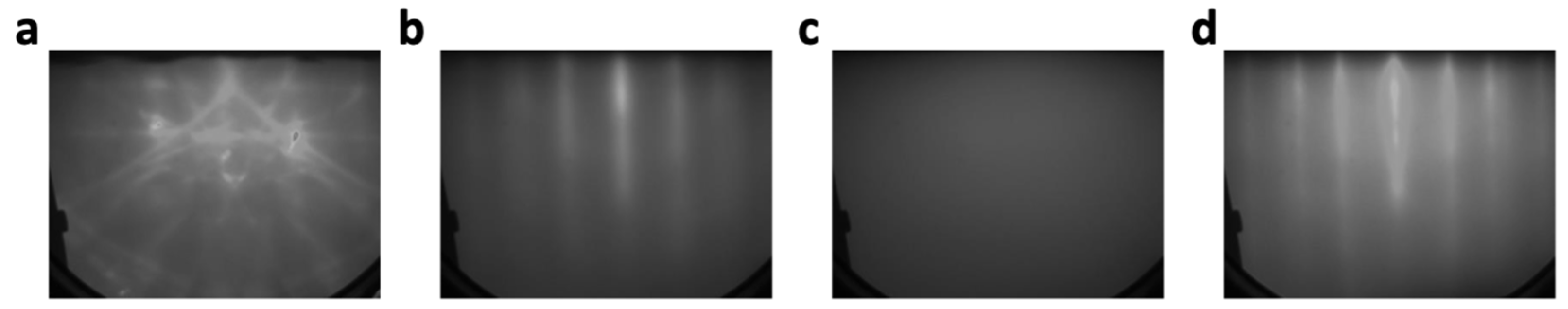
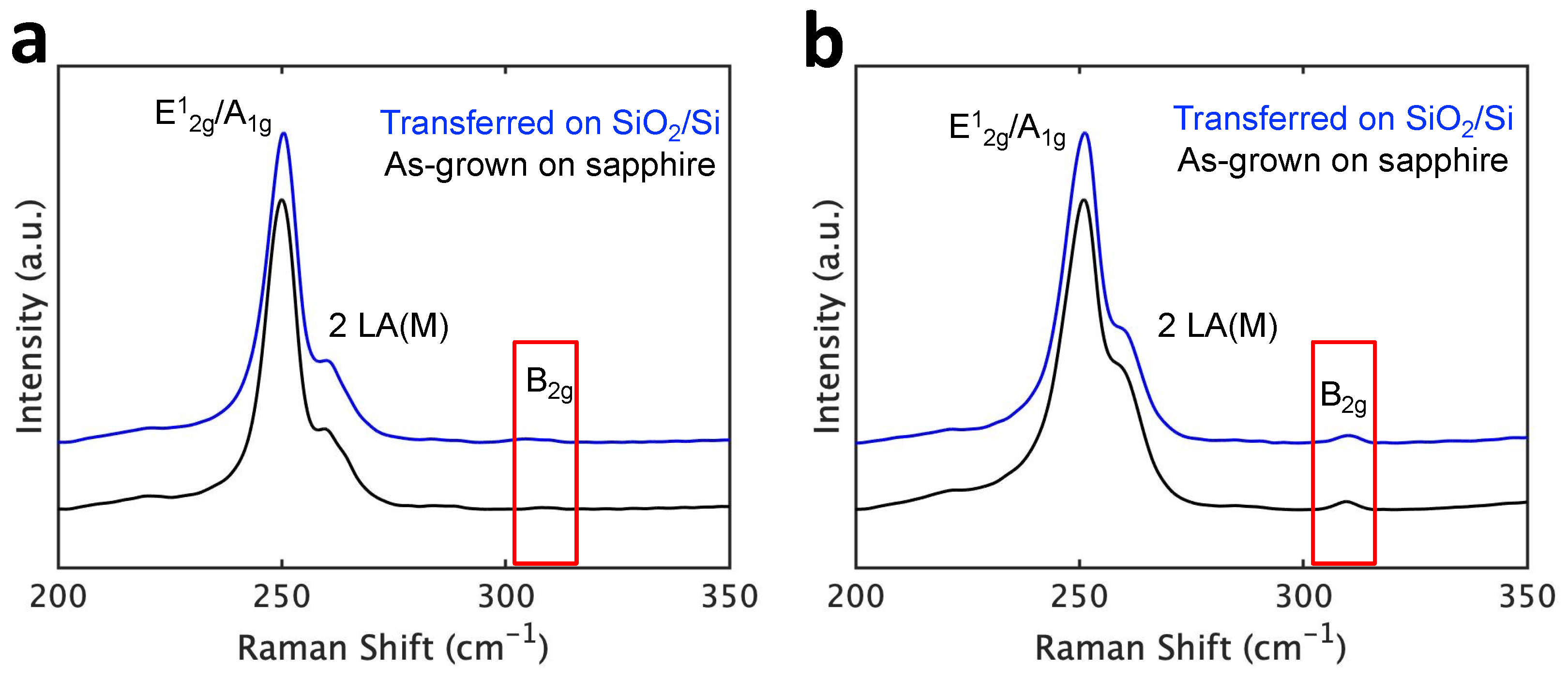
3. Results
4. Discussions
5. Conclusions
Author Contributions
Funding
Data Availability Statement
Conflicts of Interest
Abbreviations
| MBE | Molecular beam epitaxy; |
| MoSe2 | Molybdenum diselenide; |
| RHEED | Reflection high-energy electron diffraction; |
| WSe2 | Tungsten diselenide. |
References
- Novoselov, K.S.; Geim, A.K.; Morozov, S.V.; Jiang, D.; Zhang, Y.; Dubonos, S.V.; Grigorieva, I.V.; Firsov, A.A. Electric Field Effect in Atomically Thin Carbon Films. Science 2004, 306, 666–669. [Google Scholar] [CrossRef] [PubMed]
- Mbayachi, V.B.; Ndayiragije, E.; Sammani, T.; Taj, S.; Mbuta, E.R.; Khan, A.U. Graphene Synthesis, Characterization and Its Applications: A Review. Results Chem. 2021, 3, 100163. [Google Scholar] [CrossRef]
- Lin, Y.-C.; Torsi, R.; Younas, R.; Hinkle, C.L.; Rigosi, A.F.; Hill, H.M.; Zhang, K.; Huang, S.; Shuck, C.E.; Chen, C.; et al. Recent Advances in 2D Material Theory, Synthesis, Properties, and Applications. ACS Nano 2023, 17, 9694–9747. [Google Scholar] [CrossRef]
- Bhimanapati, G.R.; Lin, Z.; Meunier, V.; Jung, Y.; Cha, J.; Das, S.; Xiao, D.; Son, Y.; Strano, M.S.; Cooper, V.R.; et al. Recent Advances in Two-Dimensional Materials beyond Graphene. ACS Nano 2015, 9, 11509–11539. [Google Scholar] [CrossRef]
- Shanmugam, V.; Mensah, R.A.; Babu, K.; Gawusu, S.; Chanda, A.; Tu, Y.; Neisiany, R.E.; Försth, M.; Sas, G.; Das, O. A Review of the Synthesis, Properties, and Applications of 2D Materials. Part. Part. Syst. Charact. 2022, 39, 2200031. [Google Scholar] [CrossRef]
- Molaei, M.J.; Younas, M.; Rezakazemi, M. A Comprehensive Review on Recent Advances in Two-Dimensional (2D) Hexagonal Boron Nitride. ACS Appl. Electron. Mater. 2021, 3, 5165–5187. [Google Scholar] [CrossRef]
- Kumbhakar, P.; Jayan, J.S.; Sreedevi Madhavikutty, A.; Sreeram, P.R.; Saritha, A.; Ito, T.; Tiwary, C.S. Prospective Applications of Two-Dimensional Materials beyond Laboratory Frontiers: A Review. iScience 2023, 26, 106671. [Google Scholar] [CrossRef] [PubMed]
- Khan, K.; Tareen, A.K.; Aslam, M.; Wang, R.; Zhang, Y.; Mahmood, A.; Ouyang, Z.; Zhang, H.; Guo, Z. Recent Developments in Emerging Two-Dimensional Materials and Their Applications. J. Mater. Chem. C Mater. 2020, 8, 387–440. [Google Scholar] [CrossRef]
- Carvalho, A.; Wang, M.; Zhu, X.; Rodin, A.S.; Su, H.; Castro Neto, A.H. Phosphorene: From Theory to Applications. Nat. Rev. Mater. 2016, 1, 16061. [Google Scholar] [CrossRef]
- Hou, C.; Tai, G.; Hao, J.; Sheng, L.; Liu, B.; Wu, Z. Ultrastable crystalline semiconducting hydrogenated borophene. Angew. Chem. Int. Ed. 2020, 59, 10819–10825. [Google Scholar] [CrossRef]
- Hou, C.; Tai, G.; Liu, Y.; Wu, Z.; Liang, X.; Liu, X. Borophene-Based Materials for Energy, Sensors and Information Storage Applications. Nano Res. Energy 2023, 2, e9120051. [Google Scholar] [CrossRef]
- Manzeli, S.; Ovchinnikov, D.; Pasquier, D.; Yazyev, O.V.; Kis, A. 2D Transition Metal Dichalcogenides. Nat. Rev. Mater. 2017, 2, 17033. [Google Scholar] [CrossRef]
- Choi, W.; Choudhary, N.; Han, G.H.; Park, J.; Akinwande, D.; Lee, Y.H. Recent Development of Two-Dimensional Transition Metal Dichalcogenides and Their Applications. Mater. Today 2017, 20, 116–130. [Google Scholar] [CrossRef]
- Joseph, S.; Mohan, J.; Lakshmy, S.; Thomas, S.; Chakraborty, B.; Thomas, S.; Kalarikkal, N. A Review of the Synthesis, Properties, and Applications of 2D Transition Metal Dichalcogenides and Their Heterostructures. Mater. Chem. Phys. 2023, 297, 127332. [Google Scholar] [CrossRef]
- Gong, C.; Zhang, Y.; Chen, W.; Chu, J.; Lei, T.; Pu, J.; Dai, L.; Wu, C.; Cheng, Y.; Zhai, T.; et al. Electronic and Optoelectronic Applications Based on 2D Novel Anisotropic Transition Metal Dichalcogenides. Adv. Sci. 2017, 4, 1700231. [Google Scholar] [CrossRef] [PubMed]
- Shahbaz, I.; Tahir, M.; Li, L.; Song, Y. Advancements in 2D Transition Metal Dichalcogenides (TMDs) Inks for Printed Optoelectronics: A Comprehensive Review. Mater. Today 2024, 77, 142–184. [Google Scholar] [CrossRef]
- Chhowalla, M.; Shin, H.S.; Eda, G.; Li, L.-J.; Loh, K.P.; Zhang, H. The Chemistry of Two-Dimensional Layered Transition Metal Dichalcogenide Nanosheets. Nat. Chem. 2013, 5, 263–275. [Google Scholar] [CrossRef]
- Wei, Z.; Li, B.; Xia, C.; Cui, Y.; He, J.; Xia, J.; Li, J. Various Structures of 2D Transition-Metal Dichalcogenides and Their Applications. Small Methods 2018, 2, 1800094. [Google Scholar] [CrossRef]
- Zhao, B.; Shen, D.; Zhang, Z.; Lu, P.; Hossain, M.; Li, J.; Li, B.; Duan, X. 2D Metallic Transition-Metal Dichalcogenides: Structures, Synthesis, Properties, and Applications. Adv. Funct. Mater. 2021, 31, 2105132. [Google Scholar] [CrossRef]
- Chen, H.; Zhang, J.; Kan, D.; He, J.; Song, M.; Pang, J.; Wei, S.; Chen, K. The Recent Progress of Two-Dimensional Transition Metal Dichalcogenides and Their Phase Transition. Crystals 2022, 12, 1381. [Google Scholar] [CrossRef]
- Chaves, A.; Azadani, J.G.; Alsalman, H.; da Costa, D.R.; Frisenda, R.; Chaves, A.J.; Song, S.H.; Kim, Y.D.; He, D.; Zhou, J.; et al. Bandgap Engineering of Two-Dimensional Semiconductor Materials. NPJ 2D Mater. Appl. 2020, 4, 29. [Google Scholar] [CrossRef]
- Mak, K.F.; Shan, J. Photonics and Optoelectronics of 2D Semiconductor Transition Metal Dichalcogenides. Nat. Photonics 2016, 10, 216–226. [Google Scholar] [CrossRef]
- Wang, Q.H.; Kalantar-Zadeh, K.; Kis, A.; Coleman, J.N.; Strano, M.S. Electronics and Optoelectronics of Two-Dimensional Transition Metal Dichalcogenides. Nat. Nanotechnol. 2012, 7, 699–712. [Google Scholar] [CrossRef]
- Younas, R.; Zhou, G.; Hinkle, C.L. A Perspective on the Doping of Transition Metal Dichalcogenides for Ultra-Scaled Transistors: Challenges and Opportunities. Appl. Phys. Lett. 2023, 122, 160504. [Google Scholar] [CrossRef]
- Husain, S.; Gupta, R.; Kumar, A.; Kumar, P.; Behera, N.; Brucas, R.; Chaudhary, S.; Svedlindh, P. Emergence of Spin–Orbit Torques in 2D Transition Metal Dichalcogenides: A Status Update. Appl. Phys. Rev. 2020, 7, 041312. [Google Scholar] [CrossRef]
- Alexeev, E.M.; Ruiz-Tijerina, D.A.; Danovich, M.; Hamer, M.J.; Terry, D.J.; Nayak, P.K.; Ahn, S.; Pak, S.; Lee, J.; Sohn, J.I.; et al. Resonantly Hybridized Excitons in Moiré Superlattices in van Der Waals Heterostructures. Nature 2019, 567, 81–86. [Google Scholar] [CrossRef] [PubMed]
- Seyler, K.L.; Rivera, P.; Yu, H.; Wilson, N.P.; Ray, E.L.; Mandrus, D.G.; Yan, J.; Yao, W.; Xu, X. Signatures of Moiré-Trapped Valley Excitons in MoSe2/WSe2 Heterobilayers. Nature 2019, 567, 66–70. [Google Scholar] [CrossRef]
- Wang, L.; Shih, E.-M.; Ghiotto, A.; Xian, L.; Rhodes, D.A.; Tan, C.; Claassen, M.; Kennes, D.M.; Bai, Y.; Kim, B.; et al. Correlated Electronic Phases in Twisted Bilayer Transition Metal Dichalcogenides. Nat. Mater. 2020, 19, 861–866. [Google Scholar] [CrossRef]
- An, L.; Cai, X.; Pei, D.; Huang, M.; Wu, Z.; Zhou, Z.; Lin, J.; Ying, Z.; Ye, Z.; Feng, X.; et al. Interaction Effects and Superconductivity Signatures in Twisted Double-Bilayer WSe2. Nanoscale Horiz. 2020, 5, 1309–1316. [Google Scholar] [CrossRef]
- Lee, S.; Seo, D.; Park, S.H.; Izquierdo, N.; Lee, E.H.; Younas, R.; Zhou, G.; Palei, M.; Hoffman, A.J.; Jang, M.S.; et al. Achieving Near-Perfect Light Absorption in Atomically Thin Transition Metal Dichalcogenides through Band Nesting. Nat. Commun. 2023, 14, 3889. [Google Scholar] [CrossRef]
- Novoselov, K.S.; Jiang, D.; Schedin, F.; Booth, T.J.; Khotkevich, V.V.; Morozov, S.V.; Geim, A.K. Two-Dimensional Atomic Crystals. Proc. Natl. Acad. Sci. USA 2005, 102, 10451–10453. [Google Scholar] [CrossRef] [PubMed]
- Radisavljevic, B.; Radenovic, A.; Brivio, J.; Giacometti, V.; Kis, A. Single-Layer MoS2 Transistors. Nat. Nanotechnol. 2011, 6, 147–150. [Google Scholar] [CrossRef] [PubMed]
- Zhang, X.; Li, Y.; Mu, W.; Bai, W.; Sun, X.; Zhao, M.; Zhang, Z.; Shan, F.; Yang, Z. Advanced Tape-Exfoliated Method for Preparing Large-Area 2D Monolayers: A Review. 2D Mater. 2021, 8, 032002. [Google Scholar] [CrossRef]
- Mag-Isa, A.E.; Kim, J.-H.; Lee, H.-J.; Oh, C.-S. A Systematic Exfoliation Technique for Isolating Large and Pristine Samples of 2D Materials. 2D Mater. 2015, 2, 34017. [Google Scholar] [CrossRef]
- Li, Y.; Kuang, G.; Jiao, Z.; Yao, L.; Duan, R. Recent Progress on the Mechanical Exfoliation of 2D Transition Metal Dichalcogenides. Mater. Res. Express 2022, 9, 122001. [Google Scholar] [CrossRef]
- Budania, P.; Baine, P.T.; Montgomery, J.H.; McNeill, D.W.; Mitchell, S.J.N.; Modreanu, M.; Hurley, P.K. Comparison between Scotch Tape and Gel-Assisted Mechanical Exfoliation Techniques for Preparation of 2D Transition Metal Dichalcogenide Flakes. Micro Nano Lett. 2017, 12, 970–973. [Google Scholar] [CrossRef]
- Budania, P.; Baine, P.T.; Montgomery, J.H.; McNeill, D.W.; Mitchell, S.J.N.; Modreanu, M.; Hurley, P.K. Effect of Post-Exfoliation Treatments on Mechanically Exfoliated MoS2. Mater. Res. Express 2017, 4, 025022. [Google Scholar] [CrossRef]
- Islam, M.A.; Serles, P.; Kumral, B.; Demingos, P.G.; Qureshi, T.; Meiyazhagan, A.; Puthirath, A.B.; Bin Abdullah, M.S.; Faysal, S.R.; Ajayan, P.M.; et al. Exfoliation Mechanisms of 2D Materials and Their Applications. Appl. Phys. Rev. 2022, 9, 041301. [Google Scholar] [CrossRef]
- Yang, H.; Qin, S.; Peng, G.; Zheng, X.; Zhang, X. Ultraviolet-Ozone Treatment for Effectively Removing Adhesive Residue on Graphene. Nano 2016, 11, 1650141. [Google Scholar] [CrossRef]
- Maurtua, C.; Zide, J.; Chakraborty, C. Molecular Beam Epitaxy and Other Large-Scale Methods for Producing Monolayer Transition Metal Dichalcogenides. J. Phys. Condens. Matter 2024, 36, 383003. [Google Scholar] [CrossRef]
- Walsh, L.A.; Addou, R.; Wallace, R.M.; Hinkle, C.L. Molecular Beam Epitaxy of Transition Metal Dichalcogenides. In Molecular Beam Epitaxy: From Research to Mass Production; Elsevier: Amsterdam, The Netherlands, 2018; pp. 515–531. [Google Scholar] [CrossRef]
- Cai, Z.; Liu, B.; Zou, X.; Cheng, H.-M. Chemical Vapor Deposition Growth and Applications of Two-Dimensional Materials and Their Heterostructures. Chem. Rev. 2018, 118, 6091–6133. [Google Scholar] [CrossRef] [PubMed]
- Tang, L.; Tan, J.; Nong, H.; Liu, B.; Cheng, H.-M. Chemical Vapor Deposition Growth of Two-Dimensional Compound Materials: Controllability, Material Quality, and Growth Mechanism. Acc. Mater. Res. 2021, 2, 36–47. [Google Scholar] [CrossRef]
- Zhang, F.; Erb, C.; Runkle, L.; Zhang, X.; Alem, N. Etchant-Free Transfer of 2D Nanostructures. Nanotechnology 2018, 29, 025602. [Google Scholar] [CrossRef] [PubMed]
- Gurarslan, A.; Yu, Y.; Su, L.; Yu, Y.; Suarez, F.; Yao, S.; Zhu, Y.; Ozturk, M.; Zhang, Y.; Cao, L. Surface-Energy-Assisted Perfect Transfer of Centimeter-Scale Monolayer and Few-Layer MoS2 Films onto Arbitrary Substrates. ACS Nano 2014, 8, 11522–11528. [Google Scholar] [CrossRef]
- Sharma, M.; Aggarwal, P.; Singh, A.; Kaushik, S.; Singh, R. Flexible, Transparent, and Broadband Trilayer Photodetectors Based on MoS2/WS2 Nanostructures. ACS Appl. Nano Mater. 2022, 5, 13637–13648. [Google Scholar] [CrossRef]
- Amani, M.; Chin, M.L.; Mazzoni, A.L.; Burke, R.A.; Najmaei, S.; Ajayan, P.M.; Lou, J.; Dubey, M. Growth-Substrate Induced Performance Degradation in Chemically Synthesized Monolayer MoS2 Field Effect Transistors. Appl. Phys. Lett. 2014, 104, 203506. [Google Scholar] [CrossRef]
- Van Der Zande, A.M.; Huang, P.Y.; Chenet, D.A.; Berkelbach, T.C.; You, Y.; Lee, G.-H.; Heinz, T.F.; Reichman, D.R.; Muller, D.A.; Hone, J.C. Grains and Grain Boundaries in Highly Crystalline Monolayer Molybdenum Disulphide. Nat. Mater. 2013, 12, 554–561. [Google Scholar] [CrossRef]
- Lim, Y.R.; Han, J.K.; Kim, S.K.; Lee, Y.B.; Yoon, Y.; Kim, S.J.; Min, B.K.; Kim, Y.; Jeon, C.; Won, S.; et al. Roll-to-Roll Production of Layer-Controlled Molybdenum Disulfide: A Platform for 2D Semiconductor-Based Industrial Applications. Adv. Mater. 2018, 30, 1705270. [Google Scholar] [CrossRef] [PubMed]
- Wang, X.; Kang, K.; Chen, S.; Du, R.; Yang, E.-H. Location-Specific Growth and Transfer of Arrayed MoS2 Monolayers with Controllable Size. 2D Mater. 2017, 4, 025093. [Google Scholar] [CrossRef]
- Wang, X.; Gong, Y.; Shi, G.; Chow, W.L.; Keyshar, K.; Ye, G.; Vajtai, R.; Lou, J.; Liu, Z.; Ringe, E.; et al. Chemical Vapor Deposition Growth of Crystalline Monolayer MoSe2. ACS Nano 2014, 8, 5125–5131. [Google Scholar] [CrossRef]
- Lin, Y.-C.; Zhang, W.; Huang, J.-K.; Liu, K.-K.; Lee, Y.-H.; Liang, C.-T.; Chu, C.-W.; Li, L.-J. Wafer-Scale MoS2 Thin Layers Prepared by MoO3 Sulfurization. Nanoscale 2012, 4, 6637–6641. [Google Scholar] [CrossRef] [PubMed]
- Panasci, S.E.; Schilirò, E.; Roccaforte, F.; Giannazzo, F. Gold-Assisted Exfoliation of Large-Area Monolayer Transition Metal Dichalcogenides: From Interface Properties to Device Applications. Adv. Funct. Mater. 2025, 35, 2414532. [Google Scholar] [CrossRef]
- Velický, M.; Donnelly, G.E.; Hendren, W.R.; McFarland, S.; Scullion, D.; DeBenedetti, W.J.I.; Correa, G.C.; Han, Y.; Wain, A.J.; Hines, M.A.; et al. Mechanism of Gold-Assisted Exfoliation of Centimeter-Sized Transition-Metal Dichalcogenide Monolayers. ACS Nano 2018, 12, 10463–10472. [Google Scholar] [CrossRef]
- Shim, J.; Bae, S.-H.; Kong, W.; Lee, D.; Qiao, K.; Nezich, D.; Park, Y.J.; Zhao, R.; Sundaram, S.; Li, X.; et al. Controlled Crack Propagation for Atomic Precision Handling of Wafer-Scale Two-Dimensional Materials. Science 2018, 362, 665–670. [Google Scholar] [CrossRef]
- Cheliotis, I.; Zergioti, I. A Review on Transfer Methods of Two-Dimensional Materials. 2D Mater. 2024, 11, 22004. [Google Scholar] [CrossRef]
- Frisenda, R.; Navarro-Moratalla, E.; Gant, P.; Pérez De Lara, D.; Jarillo-Herrero, P.; Gorbachev, R.V.; Castellanos-Gomez, A. Recent Progress in the Assembly of Nanodevices and van Der Waals Heterostructures by Deterministic Placement of 2D Materials. Chem. Soc. Rev. 2018, 47, 53–68. [Google Scholar] [CrossRef]
- Watson, A.J.; Lu, W.; Guimarães, M.H.D.; Stöhr, M. Transfer of Large-Scale Two-Dimensional Semiconductors: Challenges and Developments. 2D Mater. 2021, 8, 32001. [Google Scholar] [CrossRef]
- Pham, P.V.; Mai, T.-H.; Dash, S.P.; Biju, V.; Chueh, Y.-L.; Jariwala, D.; Tung, V. Transfer of 2D Films: From Imperfection to Perfection. ACS Nano 2024, 18, 14841–14876. [Google Scholar] [CrossRef]
- Jain, A.; Bharadwaj, P.; Heeg, S.; Parzefall, M.; Taniguchi, T.; Watanabe, K.; Novotny, L. Minimizing Residues and Strain in 2D Materials Transferred from PDMS. Nanotechnology 2018, 29, 265203. [Google Scholar] [CrossRef]
- Li, R.; Li, Z.; Pambou, E.; Gutfreund, P.; Waigh, T.A.; Webster, J.R.P.; Lu, J.R. Determination of PMMA Residues on a Chemical-Vapor-Deposited Monolayer of Graphene by Neutron Reflection and Atomic Force Microscopy. Langmuir 2018, 34, 1827–1833. [Google Scholar] [CrossRef]
- Lupina, G.; Kitzmann, J.; Costina, I.; Lukosius, M.; Wenger, C.; Wolff, A.; Vaziri, S.; Östling, M.; Pasternak, I.; Krajewska, A.; et al. Residual Metallic Contamination of Transferred Chemical Vapor Deposited Graphene. ACS Nano 2015, 9, 4776–4785. [Google Scholar] [CrossRef]
- Deng, C.; Lin, W.; Agnus, G.; Dragoe, D.; Pierucci, D.; Ouerghi, A.; Eimer, S.; Barisic, I.; Ravelosona, D.; Chappert, C.; et al. Reversible Charge-Transfer Doping in Graphene Due to Reaction with Polymer Residues. J. Phys. Chem. C 2014, 118, 13890–13897. [Google Scholar] [CrossRef]
- Huang, Y.; Pan, Y.-H.; Yang, R.; Bao, L.-H.; Meng, L.; Luo, H.-L.; Cai, Y.-Q.; Liu, G.-D.; Zhao, W.-J.; Zhou, Z.; et al. Universal Mechanical Exfoliation of Large-Area 2D Crystals. Nat. Commun. 2020, 11, 2453. [Google Scholar] [CrossRef] [PubMed]
- Gupta, P.; Dongare, P.D.; Grover, S.; Dubey, S.; Mamgain, H.; Bhattacharya, A.; Deshmukh, M.M. A Facile Process for Soak-and-Peel Delamination of CVD Graphene from Substrates Using Water. Sci. Rep. 2014, 4, 3882. [Google Scholar] [CrossRef]
- Luo, X.; Zhao, Y.; Zhang, J.; Toh, M.; Kloc, C.; Xiong, Q.; Quek, S.Y. Effects of Lower Symmetry and Dimensionality on Raman Spectra in Two-Dimensional WSe2. Phys. Rev. B Condens. Matter Mater. Phys. 2013, 88, 195313. [Google Scholar] [CrossRef]
- Terrones, H.; Del Corro, E.; Feng, S.; Poumirol, J.M.; Rhodes, D.; Smirnov, D.; Pradhan, N.R.; Lin, Z.; Nguyen, M.A.T.; Elías, A.L.; et al. New First Order Raman-Active Modes in Few Layered Transition Metal Dichalcogenides. Sci. Rep. 2014, 4, 4215. [Google Scholar] [CrossRef]
- Pan, Y.; Li, S.; Rahaman, M.; Milekhin, I.; Zahn, D.R.T. Signature of Lattice Dynamics in Twisted 2D Homo/Hetero-Bilayers. 2D Mater. 2022, 9, 045018. [Google Scholar] [CrossRef]
- Sahin, H.; Tongay, S.; Horzum, S.; Fan, W.; Zhou, J.; Li, J.; Wu, J.; Peeters, F.M. Anomalous Raman Spectra and Thickness-Dependent Electronic Properties of WSe2. Phys. Rev. B Condens. Matter Mater. Phys. 2013, 87, 165409. [Google Scholar] [CrossRef]
- Pudasaini, P.R.; Stanford, M.G.; Oyedele, A.; Wong, A.T.; Hoffman, A.N.; Briggs, D.P.; Xiao, K.; Mandrus, D.G.; Ward, T.Z.; Rack, P.D. High Performance Top-Gated Multilayer WSe2 Field Effect Transistors. Nanotechnology 2017, 28, 475202. [Google Scholar] [CrossRef]
- Zhao, W.; Ghorannevis, Z.; Amara, K.K.; Pang, J.R.; Toh, M.; Zhang, X.; Kloc, C.; Tan, P.H.; Eda, G. Lattice Dynamics in Mono- and Few-Layer Sheets of WS2 and WSe2. Nanoscale 2013, 5, 9677–9683. [Google Scholar] [CrossRef]
- Hinkle, C.L.; Sonnet, A.M.; Vogel, E.M.; McDonnell, S.; Hughes, G.J.; Milojevic, M.; Lee, B.; Aguirre-Tostado, F.S.; Choi, K.J.; Kim, H.C.; et al. GaAs Interfacial Self-Cleaning by Atomic Layer Deposition. Appl. Phys. Lett. 2008, 92, 071901. [Google Scholar] [CrossRef]
- Shallenberger, J.R. 2D Tungsten Diselenide Analyzed by XPS. Surf. Sci. Spectra 2018, 25, 14001. [Google Scholar] [CrossRef]
- Yamamoto, M.; Nakaharai, S.; Ueno, K.; Tsukagoshi, K. Self-Limiting Oxides on WSe2 as Controlled Surface Acceptors and Low-Resistance Hole Contacts. Nano Lett. 2016, 16, 2720–2727. [Google Scholar] [CrossRef] [PubMed]
- Lin, Y.C.; Bersch, B.M.; Addou, R.; Xu, K.; Wang, Q.; Smyth, C.M.; Jariwala, B.; Walker, R.C.; Fullerton-Shirey, S.K.; Kim, M.J.; et al. Modification of the Electronic Transport in Atomically Thin WSe2 by Oxidation. Adv. Mater. Interfaces 2020, 7, 2000422. [Google Scholar] [CrossRef]
- Tonndorf, P.; Schmidt, R.; Böttger, P.; Zhang, X.; Börner, J.; Liebig, A.; Albrecht, M.; Kloc, C.; Gordan, O.; Zahn, D.R.T.; et al. Photoluminescence Emission and Raman Response of Monolayer MoS2, MoSe2, and WSe2. Opt. Express 2013, 21, 4908. [Google Scholar] [CrossRef]
- Pan, Y.; Zahn, D.R.T. Raman Fingerprint of Interlayer Coupling in 2D TMDCs. Nanomaterials 2022, 12, 3949. [Google Scholar] [CrossRef] [PubMed]
- Sharma, V.; Mitlin, D.; Datta, D. Understanding the Strength of the Selenium–Graphene Interfaces for Energy Storage Systems. Langmuir 2021, 37, 2029–2039. [Google Scholar] [CrossRef]
- Waitkins, G.R.; Clark, C.W. Selenium Dioxide: Preparation, Properties, and Use as Oxidizing Agent. Chem. Rev. 1945, 36, 235–289. [Google Scholar] [CrossRef]
- Onishi, S.; Ugeda, M.M.; Zhang, Y.; Chen, Y.; Ojeda-Aristizabal, C.; Ryu, H.; Mo, S.; Hussain, Z.; Shen, Z.; Crommie, M.F.; et al. Selenium Capped Monolayer NbSe2 for Two-dimensional Superconductivity Studies. Phys. Status Solidi (b) 2016, 253, 2396–2399. [Google Scholar] [CrossRef]


| Polymer-Assisted Transfer | Metal-Assisted Transfer | Liquid-Phase Transfer | Se-Assisted Transfer | |
|---|---|---|---|---|
| Defect density | High [39] | Low [64] | Low [36] | Low |
| Yield | 95% [45] | 70–99.5% [54,64] | 90% [65] | 100% |
| Contamination level | High | Low | Low | Very low |
| Advantage | Low cost | Easily scalable | Low cost | Easily scalable; best for clean transfer |
| Disadvantage | Small flake size; carbon contamination | Metal contamination | Complex process; challenging scalability | Selenide preferred |
Disclaimer/Publisher’s Note: The statements, opinions and data contained in all publications are solely those of the individual author(s) and contributor(s) and not of MDPI and/or the editor(s). MDPI and/or the editor(s) disclaim responsibility for any injury to people or property resulting from any ideas, methods, instructions or products referred to in the content. |
© 2025 by the authors. Licensee MDPI, Basel, Switzerland. This article is an open access article distributed under the terms and conditions of the Creative Commons Attribution (CC BY) license (https://creativecommons.org/licenses/by/4.0/).
Share and Cite
Younas, R.; Zhou, G.; Hinkle, C.L. Scalable and Contamination-Free Selenium-Assisted Exfoliation of Transition Metal Dichalcogenides WSe2 and MoSe2. Processes 2025, 13, 791. https://doi.org/10.3390/pr13030791
Younas R, Zhou G, Hinkle CL. Scalable and Contamination-Free Selenium-Assisted Exfoliation of Transition Metal Dichalcogenides WSe2 and MoSe2. Processes. 2025; 13(3):791. https://doi.org/10.3390/pr13030791
Chicago/Turabian StyleYounas, Rehan, Guanyu Zhou, and Christopher L. Hinkle. 2025. "Scalable and Contamination-Free Selenium-Assisted Exfoliation of Transition Metal Dichalcogenides WSe2 and MoSe2" Processes 13, no. 3: 791. https://doi.org/10.3390/pr13030791
APA StyleYounas, R., Zhou, G., & Hinkle, C. L. (2025). Scalable and Contamination-Free Selenium-Assisted Exfoliation of Transition Metal Dichalcogenides WSe2 and MoSe2. Processes, 13(3), 791. https://doi.org/10.3390/pr13030791