Abstract
The development of ultraflexible and sensitive gas sensors is critical for advancing next-generation environmental monitoring and healthcare diagnostics. In this work, we demonstrate an ultraflexible chemiresistive nitrogen dioxide (NO2) sensor integrated with a photopatterned porous poly(3-hexylthiophene) (P3HT)/SU-8 blend film as an active sensing layer. The porous microarchitecture was fabricated via high-resolution photolithography, utilizing SU-8 as a photoactive porogen to template a uniform, interconnected pore network within the P3HT matrix. The engineered porosity level ranged from 0% to 36%, substantially improving gas diffusion kinetics to enlarge the accessible surface area for analyte adsorption. Our sensor exhibited a marked enhancement in sensitivity at an optimized porosity of 36%, with the current response at 30 ppm NO2 increasing from 354% to 3201%, along with a detection limit of 0.7 ppb. The device further exhibited a high selectivity against common interfering gases, including NH3, H2S, and SO2. Moreover, the porous structure imparted excellent mechanical durability, maintaining over 90% of its initial sensing performance after 500 bending cycles at a 1 mm radius, underscoring its potential for integration into next-generation wearable environmental monitoring platforms.
1. Introduction
The rapid and precise detection of nitrogen dioxide (NO2), which is a toxic, highly reactive atmospheric pollutant primarily originating from fossil fuel combustion, vehicular emissions, and industrial activities, is critically important for environmental surveillance, public health, and occupational safety [1,2,3,4]. Chronic exposure to concentrations of NO2 as low as sub-ppm has been implicated in a range of adverse health effects, including respiratory inflammation, reduced lung function, and heightened susceptibility to airborne infections [5,6,7]. Accordingly, there is a growing demand for portable, high-performance gas sensors—or electronic noses—capable of detecting trace levels of NO2 under ambient conditions [8]. However, conventional medical-level gas sensing technologies often face substantial limitations: rigid device architectures [9], complex fabrication procedures [10], and limited mechanical adaptability collectively hinder their deployment in emerging wearable and conformable electronic platforms [11,12]. To address these challenges, a broad spectrum of NO2 sensing technology has been developed, encompassing electrochemical [13,14], optical [15,16], piezoelectric [17,18], chemiresistive [19,20,21], and more recently, transistor-based systems [22,23,24]. Each modality exploits a distinct signal transduction mechanism and offers specific trade-offs with respect to sensitivity, selectivity, scalability, and environmental operability. Among these, chemiresistive sensors have garnered significant attention due to their operational simplicity, low driving voltage, and compatibility with ultrathin, mechanically flexible substrates [19]. These sensors function by monitoring resistance changes in the active material upon gas adsorption, and typically employ semiconducting materials such as metal oxides, carbon-based nanomaterials, two-dimensional materials, or conjugated polymers [7,25,26,27]. In particular, semiconducting polymers offer several unique advantages, including solution processability, molecular tunability, and compatibility with low-temperature, large-area fabrication techniques. Moreover, their intrinsic mechanical compliance and low Young’s modulus render them ideal candidates for integration into deformable and stretchable sensing platforms [28].
Despite these benefits, critical challenges remain unresolved, particularly in achieving high sensitivity for NO2 at low concentrations, ensuring operational stability under mechanical strain, and developing scalable fabrication strategies for device integration. Recent efforts have focused on the microstructural engineering of the sensing layer to enhance analyte diffusion, improve polymer–gas interactions, and stabilize electrical responses [29,30,31]. Porous architectures, especially those with ordered features, have demonstrated substantial promise in this context. Among them, honeycomb-like microstructures, comprising periodic, hexagonally arranged through-pores, are particularly advantageous due to their high surface-area-to-volume ratios, reduced diffusion barriers, and capacity to accommodate mechanical deformation via distributed strain dissipation [21,32,33]. Nevertheless, the fabrication of highly ordered, porous polymer films on ultrathin and flexible substrates remains technically challenging [34,35]. Conventional approaches such as breath figure templating, phase separation, and sacrificial templating can introduce porosity, but often suffer from poor spatial control, limited reproducibility, and incompatibility with large-area processing [36,37,38]. UV-induced crosslinking presents a compelling alternative, providing high spatial precision, structural tunability, and compatibility with scalable, low-temperature processing [39,40]. Such merits in microstructural design and patterning strategies are pivotal for the development of next-generation NO2 sensors that combine high analytical performance with mechanical adaptability and integration readiness for wearable electronics.
Herein we present an ultraflexible chemiresistive NO2 sensor that incorporates a photopatterned, porous poly(3-hexylthiophene) (P3HT)/SU-8 composite film as the gas sensing layer. The porous microarchitecture is realized via high-resolution photolithography, where SU-8 functions as a photoactive porogen to template a uniform and interconnected pore network within the semiconducting P3HT matrix. By precisely controlling the porosity from 0% to 36%, we substantially enhance gas diffusion dynamics and increase the available surface area for analyte adsorption. At an optimized porosity of 36%, the sensor exhibits a nine-fold increase in sensitivity, with the normalized resistance response (ΔR/R0) at 30 ppm NO2 rising from 354% (dense P3HT) to 3201% (porous P3HT/SU-8 blend), while achieving a detection limit below 200 ppb. The device also displays excellent selectivity against common interfering gases, including NH3, H2S, and SO2. Critically, the porous framework imparts outstanding mechanical resilience, retaining over 90% of its original sensing performance after 500 bending cycles at a 1 mm radius, highlighting its suitability for conformal integration into next-generation wearable platforms for real-time environmental monitoring.
2. Materials and Methods
Materials and chemicals: The organic semiconductor P3HT used for gas sensing was sourced from Sigma-Aldrich. The SU-8 2002 photoresist employed for photopatterning, along with the negative photoresist nLOF 2035 and its corresponding developer AZ MIF 300, was purchased from MicroChem. All solvents used in this experimental part, including isopropanol, chloroform, and acetone, were obtained from Sigma-Aldrich.
Sensor fabrication: To fabricate the ultraflexible NO2 sensor, a 120 μm thick sacrificial layer of Micro-90 was first spin-coated onto a pre-cleaned Si/100 nm SiO2 substrate and thermally dried at 100 °C for 1 min. An ultrathin Parylene film (3 μm) was subsequently deposited to serve as a mechanically compliant support layer. Gold electrodes were then defined on the Parylene surface via a standard photolithographic lift-off process. Specifically, a layer of nLOF 2035 negative photoresist was spin-coated (500 rpm for 5 s, followed by 3000 rpm for 55 s), soft-baked at 110 °C for 60 s, and exposed to 365 nm UV light (140 mJ) through a patterned photomask. After post-exposure baking (110 °C, 60 s), the pattern was developed in MIF300 for 40 s to reveal the electrode regions. A thin adhesion layer of chromium (3 nm) and gold (50 nm) was then deposited by thermal evaporation. Lift-off in acetone removed the excess metal and photoresist, yielding well-defined Au electrode patterns. Subsequently, a P3HT/SU-8 mixed solution with varying ratios was spin-coated at 3000 rpm onto the electrode-patterned substrate to form the active sensing layer. The film was photopatterned under UV exposure (365 nm, 4800 mJ), followed by development in chloroform to yield a porous and patterned semiconducting structure. Finally, the entire device was gently delaminated from the substrate in deionized water, releasing an ultraflexible, free-standing NO2 sensor suitable for environmental monitoring.
Film and device characterization: To investigate surface morphologies, both dense and porous P3HT/SU-8 blend films were examined using a scanning electron microscope (Gemini SEM 300) and atomic force microscopy (AFM, Bruker, Billerica, MA, USA). To pattern the blend films, P3HT was first dissolved in chloroform at a concentration of 6 mg/mL; this solution was then mixed with SU-8 at a mass ratio of 20:1 (P3HT:SU-8) to generate porous microstructures upon spin-coating and subsequent development. Gas sensing measurements were conducted in a sealed testing chamber with an internal volume of approximately 0.02 L. Pre-mixed dry air and target analytes—including NO2, SO2, NH3, and H2S—were introduced into the chamber at a controlled flow rate of 100 standard cm3 min−1 using a mass flow controller to ensure consistent gas delivery. The humidity atmosphere was controlled by bubbling the air with distilled water and calibrated using a high-accuracy hygrometer (Rotronic, HC2-S, Huntington, NY, USA); the variation in relative humidity (RH) was obtained by regulating the mass flow ratio of dry air, humid air, and target NO2 gas. To ensure the rapid and complete removal of gas after each exposure, the test chamber was immediately purged with dry air at a flow rate of 500 sccm for 300 s once the target gas inlet was closed. This purge duration was more than an order of magnitude longer than the sensor’s electrical recovery time, thereby guaranteeing full desorption before the next measurement cycle. The chemiresistive responses of the ultraflexible sensors were evaluated using a semiconductor parameter analyzer (Keithley 4200-SCS, Germering, Germany) under ambient conditions (25 °C).
3. Results and Discussions
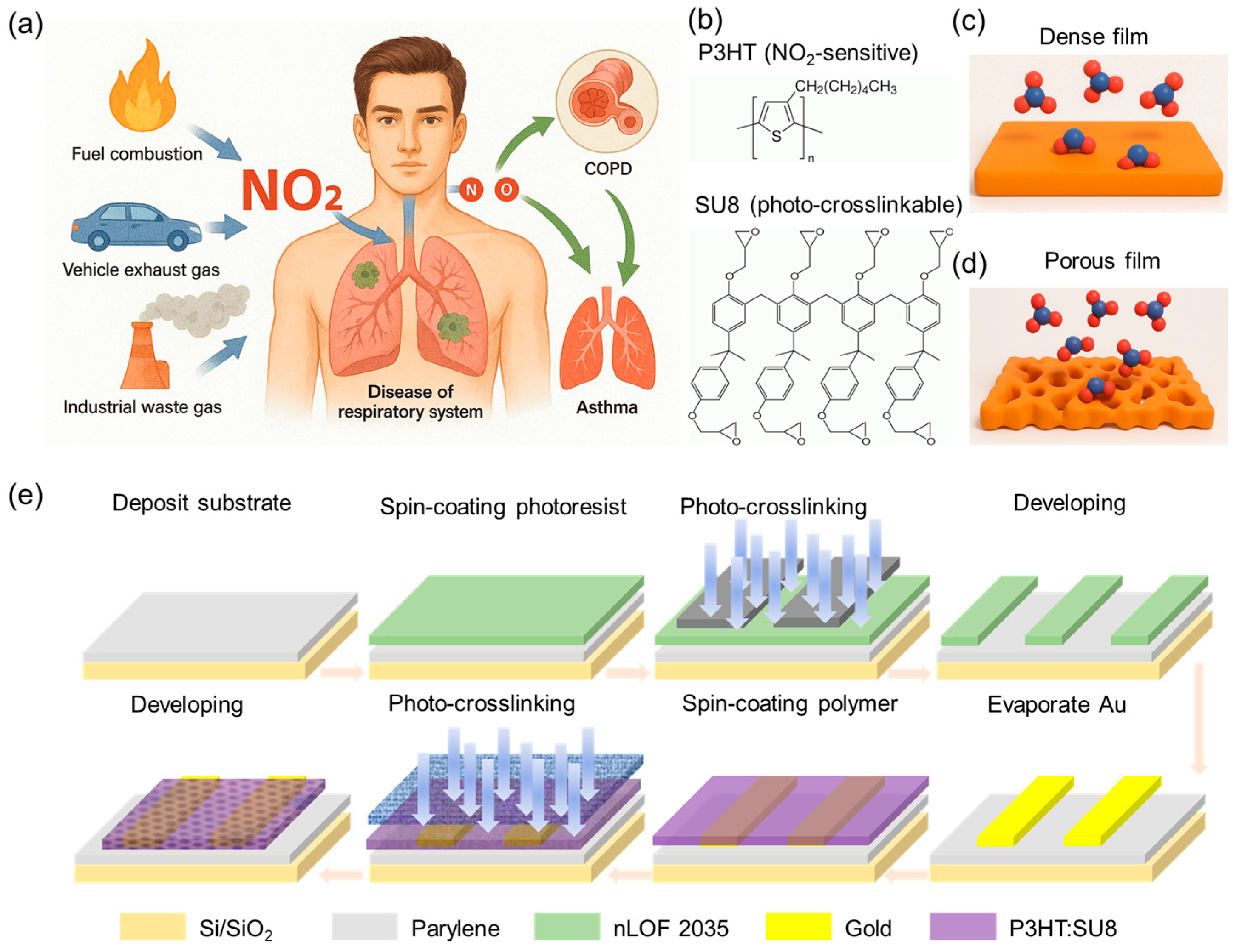
NO2 from fuel combustion, industry, and traffic seriously harms health, penetrating alveoli to trigger oxidative stress, inflammation, and worsening COPD or asthma. Urgent on-body monitoring demands ultraflexible, low-voltage, high-sensitivity NO2 sensors (Figure 1a). Thus, we introduce a photo-crosslinkable polymer matrix (SU-8) and gas-sensitive semiconducting (P3HT) components to create a porous, high-surface-area morphology tailored for enhanced gas sorption and efficient charge transport. Its chemical structure is illustrated in Figure 1b. This design contrasts the compact, diffusion-limited morphology of conventional dense film with a porous structure that allows for efficient gas ingress and increased molecular access to redox-active sites in semiconductor bulk, thereby enabling more sensitive electronic response (Figure 1c,d). To translate this material innovation into a scalable sensing platform, we established a fully solution-processable and photopatternable fabrication strategy for a porous chemiresistive NO2 gas sensor (Figure 1e, see Materials and Methods for fabrication details). Central to this approach is the development of a photo-crosslinkable semiconducting polymer, which undergoes in situ crosslinking upon UV exposure using a predesigned photomask with variable porosity (Figure S1). This process not only enables effective template removal but also yields a micropatterned, nanostructured semiconducting film with a high surface-to-volume ratio and excellent mechanical robustness. The resulting P3HT/SU-8 porous architecture imparts several advantages: (i) enhanced NO2 gas permeability and accelerated redox kinetics for sensitive NO2 detection; (ii) a mechanically resilient crosslinked network that preserves structural integrity under repeated mechanical deformation, ensuring compatibility with wearable and flexible electronics; (iii) a crosstalk-free, high-resolution patterning strategy that supports sensor integration using fully solution-based processes where required.
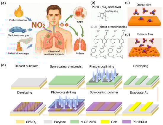
Figure 1.
Design concept and fully photolithographic fabrication of porous chemiresistive NO2 sensor. (a) Schematic representation of major environmental sources of NO2. (b) Molecular structures of semiconducting polymer P3HT and photo-crosslinkable resin SU-8. (c,d) Schematic comparison of NO2 diffusion and interaction at semiconductor interface in dense P3HT films (c) versus photopatterned porous P3HT/SU-8 composites (d). (e) Stepwise fabrication procedure of patterned porous chemiresistive sensor via all-photolithographic process.
To systematically validate the porosity properties of the patterned P3HT/SU-8 blend films, a suite of optical, electron microscopy, and spectroscopic analyses were conducted across porosity levels ranging from 0% to 36%. Note that porosity is defined as the ratio of the total pore area to the total area of the sensing film, as observed from top-view microscopy images. As illustrated in Figure 2a, optical microscopy images reveal the progressive emergence of highly ordered, hexagonally arranged through-pores with increasing porosity. The successful realization of a periodic honeycomb-like architecture, with feature sizes below 5 μm, confirms the high-fidelity photopatternability of the polymer blend and highlights the exceptional resolution achievable via SU-8 photo-crosslinking. SEM (Figure 2b) images further confirm the morphology of the films, revealing an interconnected porous network whose density and uniformity increase with porosity. Notably, no signs of pore collapse or film delamination are observed, even at the highest porosity (36%), underscoring the mechanical robustness of the crosslinked framework. These through-pores are expected to substantially reduce diffusion barriers for NO2 gas molecules, enabling deeper analyte penetration and enhanced redox interaction across the film’s thickness. The elemental mapping of carbon (C) via energy-dispersive X-ray spectroscopy (EDS) (Figure 2c) confirms the spatial fidelity of the photopatterned porous architecture. Carbon signals, predominantly originating from the P3HT/SU-8 domains, show an inverse correlation with the pore network, validating the selective removal of the un-exposed regions.
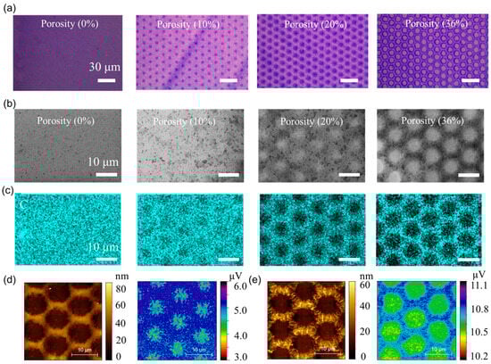
Figure 2.
Morphological and elemental analysis of photopatterned porous P3HT/SU-8 sensing films. (a) Optical microscopy images of photopatterned P3HT/SU-8 blend films. (b) Corresponding SEM images reveal evolution of microstructural features with increasing porosity. (c) Energy-dispersive X-ray spectroscopy (EDS) mapping of carbon (C) confirms spatial distribution across varying porosity conditions. (d) Atomic force microscopy (AFM) and Kelvin probe force microscopy (KPFM) measurements of 36% porosity film. (e) AFM and KPFM measurements of 36% porosity film after NO2 absorption.
Complementary EDS maps for silicon (Si) and oxygen (O) (Figure S2) provide further insight into the pore formation mechanism: the Si signal (from the underlying substrate) is intensified in the pore regions, whereas the O signal remains uniformly distributed, corresponding to residual crosslinked SU-8 at the pore periphery and confirming the structural continuity of the matrix. Topographical analysis via atomic AFM (Figure 2d, left) reveals a uniform pore morphology with a film thickness of approximately 80 nm, ensuring a low diffusion distance for NO2 molecules while maintaining adequate mechanical compliance for a flexible sensor. Kelvin probe force microscopy (KPFM) (Figure 2d, right) maps the surface potential distribution, indicating localized regions of higher work function within the pore walls—suggesting preferential NO2 adsorption and redox interaction sites. More importantly, a direct visual comparison clearly highlights the surface potential shift (from 5.2 μV to 10.8 μV) induced by NO2 adsorption, supporting our interpretation of charge transfer and doping effects (Figure 2e). These results elucidate the structural–functional relationship between engineered porosity and enhanced chemiresistive sensing performance, with the patterned pores serving as efficient molecular conduits and adsorption centers.
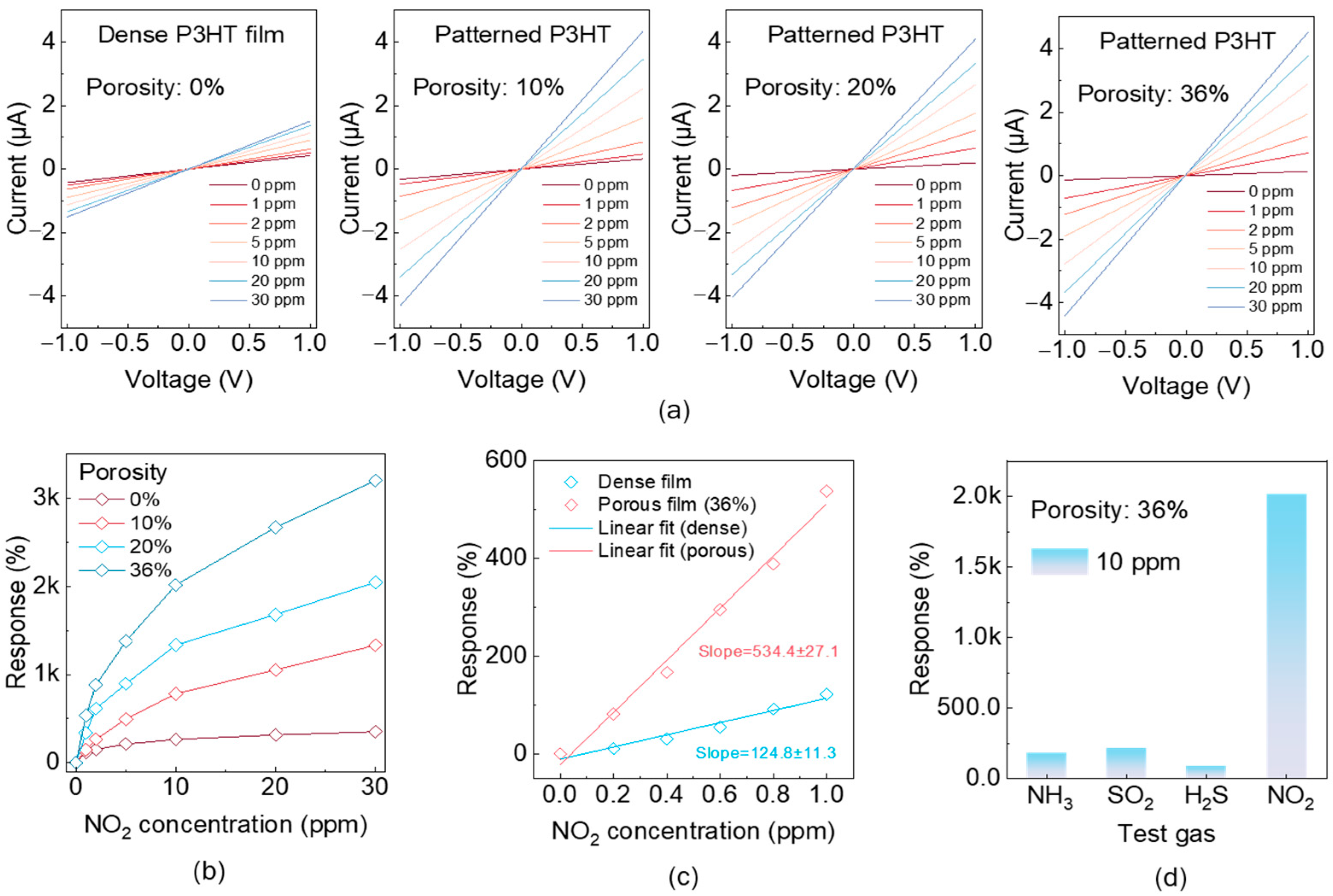
To elucidate the role of nanostructured porosity via the photopattern technique in modulating analyte transport and sensing performance, a systematic investigation was conducted on chemiresistive NO2 sensors fabricated with controlled porosity levels of 0%, 10%, 20%, and 36%. Figure 3a presents the response profiles of the four sensors upon exposure to varying NO2 concentrations (1–30 ppm), with the normalized current change (I/I0) plotted as a function of voltage, where I0 is the baseline current measured in dry air after 300 s stabilization and I is the steady-state current recorded after 300 s of exposure to NO2 at the specified concentration. The dense film sensor (0% porosity) exhibits a markedly low response, reaching only ~353% at 30 ppm, with substantial signal overlap across concentrations—indicative of limited NO2 diffusion and poor surface accessibility. In contrast, sensors with 10% and 20% porosity demonstrate significantly enhanced signal separation and higher saturation amplitudes, reflecting improved gas permeability and more efficient analyte adsorption on the active sensing layer. These results confirm that moderate porosity optimizes the trade-off between surface area accessibility and structural/electronic continuity. Notably, the sensor with 36% porosity achieves the highest response amplitude, reaching ~3201% at 30 ppm—approximately 9-fold greater than that of the dense film—highlighting the critical role of engineered nano-porosity in amplifying chemiresistive sensitivity. Note that as the porosity of the active layer increases from 0% to 10%, 20%, and 36%, the corresponding channel current decreases from 0.43 µA to 0.32 µA, 0.20 µA, and 0.14 µA under 1 V bias and 0 ppm NO2 concentration conditions, indicating a clear increase in resistivity, thus enhancing the response ability. Figure 3b presents the steady-state responses of sensors with varying porosity levels as a function of NO2 concentration. All the response curves exhibit a non-linear yet monotonic increase with rising NO2 levels. Notably, sensors with higher porosity demonstrate markedly steeper response slopes, with the 36% porosity device achieving substantially greater signal amplitudes across the entire concentration range. This enhancement in both slope and response magnitude underscores the role of porosity in promoting gas–surface interaction kinetics and facilitating the more complete utilization of the sensing film’s active sites. The pronounced increase in slope with porosity substantiates the design strategy of microstructural tuning to improve detection performance without modifying the intrinsic sensing chemistry.
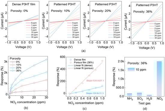
Figure 3.
Chemiresistive sensing performance of porosity-engineered NO2 sensors. (a) Dynamic resistance response (ΔR/R0) of sensors fabricated with varying porosity levels (0%, 10%, 20%, and 36%) upon exposure to NO2 gas. (b) Steady-state response amplitudes as functions of NO2 concentration. (c) Linear regression analysis of low-concentration range for dense (0%) and 36% porosity sensors. (d) Selectivity evaluation of 36% porous sensor in presence of 10 ppm NO2 versus typical interfering gases, including NH3, H2S, and SO2.
To quantify the detection limit, Figure 3c displays the linear response fits within the low-concentration regime (0–1 ppm) for the devices with the dense and 36% porosity films. The slope of the response–concentration curve increases markedly from 124.8 ± 11.3 (dense, 0% porosity) to 534.4 ± 37.1 (36% porosity), indicating a more than four-fold enhancement in sensitivity. This linear regime is particularly critical for practical sensing applications, as it defines the calibration window and determines the minimum concentration change that can be reliably detected. Notably, the porous architecture enables a response approaching 100 even at concentrations as low as 0.2 ppm, indicating the capability of the photopatterned porous structure to achieve ultralow detection limits. By combining the sensor’s baseline noise measurements in the absence of NO2, the limit of detection (LOD) was estimated to be approximately 0.7 ppb (Figure S3). Next, to broaden the practical applications of our sensor, NO2 needed to be selectively distinguished from other chemically reactive gases that (i) occur at comparable ambient concentrations, (ii) exhibit similar oxidizing or reducing behavior, (iii) interact with the P3HT/SU-8 semiconducting blend. Figure 3d evaluates the chemical selectivity of the sensor by comparing its response to 10 ppm of NO2 against several representative interfering gases, including NH3, H2S, and SO2. The sensor exhibits a markedly stronger response to NO2, with signal amplitudes at least an order of magnitude higher than those induced by the other analytes. This pronounced selectivity is attributed to the intrinsic redox interactions between NO2 and the sensing material, likely involving strong electron-withdrawing adsorption onto the p-type semiconducting backbone. In contrast, the interfering gases have weak electron donors or are relatively inert under ambient conditions, thus inducing minimal charge transfer and negligible sensor activation, irrespective of the material’s porosity. Such selective responsiveness is critical for practical deployment in complex, mixed-gas environments where the accurate discrimination of target analytes is essential. In addition, the influence of ambient humidity must be considered for practical deployment. Figure S4 presents the sensor’s response to varying NO2 concentrations under different relative humidity (RH) conditions. Notably, the sensing performance exhibited a gradual decline with increasing RH, indicating that the chemiresistive sensor based on the P3HT/SU-8 blend can operate reliably only within a specific humidity range. Moreover, we evaluated the response dynamics of the P3HT/SU-8-blend-based gas sensor. Owing to its highly porous microstructure, the sensor enables the rapid adsorption and desorption of gas molecules, resulting in a fast response speed, with a rise time of 30.91 s and a recovery time of 5.13 s (Figure S5). Notably, the device maintains stable operation across multiple continuous 30 ppm NO2 exposure cycles, demonstrating excellent repeatability and robustness (Figure S6).
Next, evaluating the sensor’s performance under mechanical deformation—particularly bending, which is among the most common modes of strain encountered in practical wearable and bio-integrated electronic systems—was essential for validating its real-world applicability. As shown in Figure 4a, the serpentine geometry of the interconnects enables large in-plane deformation by geometrically distributing the applied strain, minimizing localized stress concentrations, and preserving the electrical and structural integrity of the conductive pathways. Complementing this, the porous architecture of the active sensing layer, which was engineered through a P3HT/SU-8 photopatterned composite, facilitates mechanical flexibility and gas permeability.
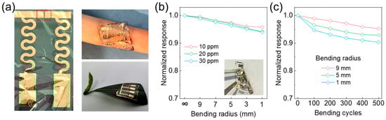
Figure 4.
Mechanical durability and reliability of ultraflexible NO2 sensor under bending deformation. (a) Optical image of fabricated device and demonstrations of conformal integration on curved surfaces. (b) Normalized resistance changes at three representative gas concentrations as functions of bending radius, showing negligible electrical degradation down to radius of 2 mm. (c) Resistance variation over 500 bending cycles.
Meanwhile, the ultrathin Parylene (3 μm) substrate enables intimate and conformal contact with arbitrarily curved or dynamically moving surfaces, such as human skin or plant leaves. This structure mitigates delamination and mechanical mismatch, thereby underscoring the system’s potential for seamless, long-term bio-integration. To systematically assess the mechanical compliance and operational reliability of the device, we characterized the NO2 sensing performance under a range of bending radii and repeated bending cycles. As illustrated in Figure 4b, the sensor maintains a stable chemiresistive response across bending radii from ∞ (flat) to 1 mm at various NO2 concentrations (10 ppm, 20 ppm, and 30 ppm), with negligible performance degradation (signal retention > 95%) throughout. This phenomenon indicates robust mechanical resilience and sensing reliability under diverse curvature scenarios relevant to conformal applications. Furthermore, long-term durability was determined by subjecting the sensor to 500 bending cycles. As shown in Figure 4c, the relative response remains above 95% of its initial value at a 9 mm bending radius and exceeds 90% even under more extreme deformation at 1 mm radius, showing excellent fatigue resistance and reliable operation under dynamic mechanical stress. Collectively, these results suggest that the sensor has mechanical robustness and long-term operational stability, promoting its application in wearable and bio-interfaced environmental monitoring platforms.
4. Conclusions
In summary, we have developed an ultraflexible chemiresistive NO2 sensor featuring a photopatterned porous P3HT/SU-8 composite film as an active layer. By leveraging SU-8 as a photoactive porogen, we achieved precise control over the microstructure, enabling uniform, interconnected porosity that significantly enhanced gas diffusion and adsorption. The optimized device, with 36% engineered porosity, exhibits a ~9× improvement in sensitivity compared to its non-porous counterpart, alongside sub 200 ppb detection limits and high selectivity against common interfering gases. Furthermore, the sensor demonstrates exceptional mechanical durability (1 mm) under repeated bending (500 cycles), highlighting its suitability for integration into next-generation wearable environmental monitoring platforms. This work establishes a scalable and versatile strategy for porosity engineering in organic semiconductors, opening new avenues for high-performance, flexible gas sensing technology.
Supplementary Materials
The following supporting information can be downloaded at: https://www.mdpi.com/article/10.3390/chemosensors13060216/s1, Figure S1: Photomask design with variable porosity used for fabricating porous film; Figure S2: Energy-dispersive X-ray spectroscopy (EDS) mappings of silicon (Si) and oxygen (O) for the 36% porosity film; Figure S3: Noise measurements under 0 ppm NO2 atmosphere to calculate the sensor’s limit of detection (LOD), where LOD≈0.7 ppb; Figure S4: Gas sensing performance of the P3HT/SU-8 blend film-based sensor (porosity = 36%) under varying relative humidity conditions; Figure S5: Response time during the gas adsorption and desorption processes of the sensor; Figure S6: Multiple continuous 30 ppm NO2 exposure-purged cycles.
Author Contributions
Conceptualization, X.Y. and J.Y.; methodology, X.Y., B.W. and L.G.; validation, X.Y. and Y.P.; formal analysis, L.G.; investigation, X.Y.; data curation, X.Y.; writing—original draft preparation, X.Y., B.W. and L.G.; writing—review and editing, Y.H. and J.Y.; supervision, J.Y.; funding acquisition, J.Y. All authors have read and agreed to the published version of the manuscript.
Funding
This work was financially supported by the National Key R&D Program of China (2022YFE0134800, 2023YFC2411800), the National Natural Science Foundation of China (No. 62273073), the Aeronautical Science Foundation of China (20230024080002), the Sichuan Science and Technology Program (No. 2023ZYD0161), and Sichuan Youth Software Innovation Project Funding (No. MZGC20240059). This work was also sponsored by the Sichuan Province Key Laboratory of Display Science and Technology.
Institutional Review Board Statement
Not applicable.
Informed Consent Statement
Not applicable.
Data Availability Statement
The original contributions presented in this study are included in the article. Further inquiries can be directed to the corresponding authors.
Conflicts of Interest
The authors declare no conflicts of interest. The funders had no role in the design of the study; in the collection, analyses, or interpretation of data; in the writing of the manuscript; or in the decision to publish the results.
References
- Ueda, T.; Boehme, I.; Hyodo, T.; Shimizu, Y.; Weimar, U.; Barsan, N. Effects of gas adsorption properties of an Au-loaded porous In2O3 sensor on NO2-sensing properties. ACS Sens. 2021, 6, 4019–4028. [Google Scholar] [CrossRef] [PubMed]
- Wang, Q.; Li, H.; Chu, J.; Pan, J.; Yang, A.; Xiao, S.; Yuan, H.; Rong, M.; Wang, X. Real-time monitoring of air discharge in a switchgear by an intelligent NO2 sensor module. ACS Sens. 2023, 8, 4646–4654. [Google Scholar] [CrossRef] [PubMed]
- Zhang, S.; Lai, X.; Xiao, R.; Pang, L.; Lu, Z.; He, X.; Gao, J. Size-dependent response of hydrothermally grown SnO2 for a high-performance NO2 sensor and the impact of oxygen. ACS Sens. 2024, 9, 195–205. [Google Scholar] [CrossRef] [PubMed]
- Goswami, P.; Gupta, G. Recent progress of flexible NO2 and NH3 gas sensors based on transition metal dichalcogenides for room temperature sensing. Mater. Today Chem. 2022, 23, 100726. [Google Scholar] [CrossRef]
- Kumar, S.; Meng, G.; Mishra, P.; Tripathi, N.; Bannov, A.G. A systematic review on 2D MoS2 for nitrogen dioxide (NO2) sensing at room temperature. Mater. Today Commun. 2023, 34, 105045. [Google Scholar] [CrossRef]
- Li, Q.; Zeng, W.; Li, Y. Metal oxide gas sensors for detecting NO2 in industrial exhaust gas: Recent developments. Sens. Actuators B Chem. 2022, 359, 131579. [Google Scholar] [CrossRef]
- Wang, X.; Chen, Y.; Zeng, Z.; Yan, M.; Jia, X.; Hu, P.; Xu, J.; Xue, Z.; Xu, J. Tailoring the injection action of oxygen over top-surface of bismuth sulfide to change reactive electron transfer path for flexible NO2 sensors. Mater. Sci. Eng. R Rep. 2024, 160, 100819. [Google Scholar] [CrossRef]
- Freddi, S.; Gonzalez, M.; Casotto, A.; Sangaletti, L.; Feyter, S. Machine-Learning-Aided NO2 Discrimination with an Array of Graphene Chemiresistors Covalently Functionalized by Diazonium Chemistry. Chem. A Eur. J. 2023, 60, e202302154. [Google Scholar] [CrossRef] [PubMed]
- Liu, C.; Wang, Q.; Wang, C.; Wang, Q.; Zhao, W.; He, Z.; Zheng, Y.; Jing, Y.; Sun, X.; Zhang, S. State of the art overview wearable biohazard gas sensors based on nanosheets for environment monitoring applications. Trends Environ. Anal. Chem. 2023, 40, e00215. [Google Scholar] [CrossRef]
- Yin, Z.; Yang, Y.; Hu, C.; Li, J.; Qin, B.; Yang, X. Wearable respiratory sensors for health monitoring. NPG Asia Mater. 2024, 16, 8. [Google Scholar] [CrossRef]
- Lee, M.Y.; Lee, H.R.; Park, C.H.; Han, S.G.; Oh, J.H. Organic transistor-based chemical sensors for wearable bioelectronics. Acc. Chem. Res. 2018, 51, 2829–2838. [Google Scholar] [CrossRef] [PubMed]
- Verma, G.; Gupta, A. Next-Generation Chemiresistive Wearable Breath Sensors for Non-Invasive Healthcare Monitoring: Advances in Composite and Hybrid Materials. Small 2025, 21, 2411495. [Google Scholar] [CrossRef]
- Khan, M.A.H.; Rao, M.V.; Li, Q. Recent advances in electrochemical sensors for detecting toxic gases: NO2, SO2 and H2S. Sensors 2019, 19, 905. [Google Scholar] [CrossRef] [PubMed]
- Fergus, J.W. Materials for high temperature electrochemical NOx gas sensors. Sens. Actuators B Chem. 2007, 121, 652–663. [Google Scholar] [CrossRef]
- Di Franco, C.; Elia, A.; Spagnolo, V.; Scamarcio, G.; Lugarà, P.M.; Ieva, E.; Cioffi, N.; Torsi, L.; Bruno, G.; Losurdo, M. Optical and electronic NOx sensors for applications in mechatronics. Sensors 2009, 9, 3337–3356. [Google Scholar] [CrossRef] [PubMed]
- Pawar, D.; Kale, S.N. A review on nanomaterial-modified optical fiber sensors for gases, vapors and ions. Microchim. Acta 2019, 186, 253. [Google Scholar]
- Zhu, Q.; Wu, T.; Wang, N. From piezoelectric nanogenerator to non-invasive medical sensor: A review. Biosensors 2023, 13, 113. [Google Scholar] [CrossRef]
- Zhao, Z.; Zhu, Q.; Lu, Y.; Mi, Y.; Cao, X.; Wang, N. Chemical sensor based on piezoelectric/triboelectric nanogenerators: A review of the modular design strategy. Chemosensors 2023, 11, 304. [Google Scholar] [CrossRef]
- Najafi, P.; Ghaemi, A. Chemiresistor gas sensors: Design, Challenges, and Strategies: A comprehensive review. Chem. Eng. J. 2024, 498, 154999. [Google Scholar] [CrossRef]
- Sharma, A.; Eadi, S.B.; Noothalapati, H.; Otyepka, M.; Lee, H.-D.; Jayaramulu, K. Porous materials as effective chemiresistive gas sensors. Chem. Soc. Rev. 2024, 53, 2530–2577. [Google Scholar] [CrossRef]
- Liu, C.; Wu, M.; Gao, L.; Liu, H.; Yu, J. Nanoporous polymer films based on breath figure method for stretchable chemiresistive NO2 gas sensors. Sens. Actuators B Chem. 2022, 371, 132540. [Google Scholar] [CrossRef]
- Kang, Y.; Kwak, D.H.; Kwon, J.E.; Kim, B.-G.; Lee, W.H. NO2-affinitive conjugated polymer for selective sub-parts-per-billion NO2 detection in a field-effect transistor sensor. ACS Appl. Mater. Interfaces 2021, 13, 31910–31918. [Google Scholar] [CrossRef]
- Zhuang, X.; Han, S.; Huai, B.; Shi, W.; Yu, J. Sub-ppm and high response organic thin-film transistor NO2 sensor based on nanofibrillar structured TIPS-pentacene. Sens. Actuators B Chem. 2019, 279, 238–244. [Google Scholar] [CrossRef]
- Sharma, N.; Kumar, S.; Gupta, A.; Dolmanan, S.B.; Patil, D.S.K.; Tan, S.T.; Tripathy, S.; Kumar, M. MoS2 functionalized AlGaN/GaN transistor based room temperature NO2 gas sensor. Sens. Actuators A Phys. 2022, 342, 113647. [Google Scholar] [CrossRef]
- Lee, S.W.; Lee, W.; Hong, Y.; Lee, G.; Yoon, D.S. Recent advances in carbon material-based NO2 gas sensors. Sens. Actuators B Chem. 2018, 255, 1788–1804. [Google Scholar] [CrossRef]
- Yang, S.; Jiang, C.; Wei, S.-H. Gas sensing in 2D materials. Appl. Phys. Rev. 2017, 4, 021304. [Google Scholar] [CrossRef]
- Wang, Z.; Huang, L.; Zhu, X.; Zhou, X.; Chi, L. An ultrasensitive organic semiconductor NO2 sensor based on crystalline TIPS-Pentacene films. Adv. Mater. 2017, 29, 1703192. [Google Scholar] [CrossRef]
- Yu, C.; He, J.H.; Cheng, X.F.; Lin, H.Z.; Yu, H.; Lu, J.M. An ion-in-conjugation-boosted organic semiconductor gas sensor operating at high temperature and immune to moisture. Angew. Chem. Int. Ed. 2021, 60, 15328–15334. [Google Scholar] [CrossRef]
- Li, M.; Hu, M.; Liu, Q.; Ma, S.; Sun, P. Microstructure characterization and NO2-sensing properties of porous silicon with intermediate pore size. Appl. Surf. Sci. 2013, 268, 188–194. [Google Scholar] [CrossRef]
- Yan, Y.; Ma, Z.; Sun, J.; Bu, M.; Huo, Y.; Wang, Z.; Li, Y.; Hu, N. Surface microstructure-controlled ZrO2 for highly sensitive room-temperature NO2 sensors. Nano Mater. Sci. 2021, 3, 268–275. [Google Scholar] [CrossRef]
- Shanmugasundaram, A.; Johar, M.A.; Paeng, C.; Jeong, Y.-J.; Abdullah, A.; Park, J.; Ryu, S.-W.; Yim, C.; Lee, D.-W. InGaN/GaN multi-quantum well nanowires: Enhanced trace-level NO2 detection for environmental and breath analysis. Chem. Eng. J. 2024, 491, 152074. [Google Scholar] [CrossRef]
- Gao, L.; Liu, C.; Peng, Y.; Deng, J.; Hou, S.; Cheng, Y.; Huang, W.; Yu, J. Ultrasensitive flexible NO2 gas sensors via multilayer porous polymer film. Sens. Actuators B Chem. 2022, 368, 132113. [Google Scholar] [CrossRef]
- Meng, W.; Wang, L.; Zhou, H.; He, Z.; Dai, L. Enhanced sensing performance of the amperometric NO2 sensor by use of a mixed conductive porous layer. Electrochim. Acta 2022, 431, 141070. [Google Scholar] [CrossRef]
- Liu, C.; Deng, J.; Gao, L.; Cheng, J.; Peng, Y.; Zeng, H.; Huang, W.; Feng, L.W.; Yu, J. Multilayer Porous Polymer Films for High-Performance Stretchable Organic Electrochemical Transistors. Adv. Electron. Mater. 2023, 9, 2300119. [Google Scholar] [CrossRef]
- Peng, Y.; Gao, L.; Liu, C.; Deng, J.; Xie, M.; Bai, L.; Wang, G.; Cheng, Y.; Huang, W.; Yu, J. Stretchable organic electrochemical transistors via three-dimensional porous elastic semiconducting films for artificial synaptic applications. Nano Res. 2023, 16, 10206–10214. [Google Scholar] [CrossRef]
- Cheng, N.; Miao, D.; Wang, C.; Lin, Y.; Babar, A.A.; Wang, X.; Wang, Z.; Yu, J.; Ding, B. Nanosphere-structured hierarchically porous PVDF-HFP fabric for passive daytime radiative cooling via one-step water vapor-induced phase separation. Chem. Eng. J. 2023, 460, 141581. [Google Scholar] [CrossRef]
- Huang, L.; Wang, Z.; Chen, J.; Wang, B.; Chen, Y.; Huang, W.; Chi, L.; Marks, T.J.; Facchetti, A. Porous Semiconducting Polymers Enable High-Performance Electrochemical Transistors. Adv. Mater. 2021, 33, 2007041. [Google Scholar] [CrossRef] [PubMed]
- Huang, J.; Liu, C.; Jin, Y.; Chen, J. Hierarchical porous carbon synthesis by carbonized polymer dots-based sacrificial template for high-performance supercapacitors. Chem. Eng. J. 2023, 461, 141930. [Google Scholar] [CrossRef]
- Gao, L.; Zhang, Q.; Lai, Y.; Xie, M.; Liu, C.; Zhang, D.; Peng, Y.; Bai, L.; Wu, M.; Feng, L.-W. High-loading homogeneous crosslinking enabled ultra-stable vertical organic electrochemical transistors for implantable neural interfaces. Nano Energy 2024, 129, 110062. [Google Scholar] [CrossRef]
- Mooney, M.; Crep, C.; Rondeau-Gagné, S. Materials Design Strategies for Solvent-Resistant Organic Electronics. ACS Appl. Electron. Mater. 2022, 4, 5652–5663. [Google Scholar] [CrossRef]


Disclaimer/Publisher’s Note: The statements, opinions and data contained in all publications are solely those of the individual author(s) and contributor(s) and not of MDPI and/or the editor(s). MDPI and/or the editor(s) disclaim responsibility for any injury to people or property resulting from any ideas, methods, instructions or products referred to in the content. |
© 2025 by the authors. Licensee MDPI, Basel, Switzerland. This article is an open access article distributed under the terms and conditions of the Creative Commons Attribution (CC BY) license (https://creativecommons.org/licenses/by/4.0/).