Review

Gate Engineering in Two-Dimensional (2D) Channel FET Chemical Sensors: A Comprehensive Review of Architectures, Mechanisms, and Materials

by
Ganapathi Bharathi
1 and
Seongin Hong
1,2,*
1
Department of Physics and Semiconductor Science, Gachon University, Seongnam 13120, Republic of Korea
2
Department of Semiconductor Engineering, Gachon University, Seongnam 13120, Republic of Korea
*
Author to whom correspondence should be addressed.
Chemosensors 2025, 13(6), 217; https://doi.org/10.3390/chemosensors13060217
Submission received: 5 May 2025 / Revised: 5 June 2025 / Accepted: 11 June 2025 / Published: 13 June 2025

Abstract

:
Field-effect transistor (FET) chemical sensors are essential for enabling sophisticated lifestyles and ensuring safe working environments. They can detect a wide range of analytes, including gaseous species (NO2, NH3, VOCs), ionic compounds, and biological molecules. Among the structural components of FETs, the gate configuration plays a vital role in controlling the semiconductor channel’s electrostatic environment, thereby strongly influencing sensing performance. Two-dimensional (2D) materials offer additional advantages in these sensors due to their rich surface chemistry and high sensitivity to external interactions. This review offers a comprehensive classification of 2D channel FET chemical sensors based on their gate configurations. Their working principles, fabrication strategies, and sensing performance are discussed in detail. A critical analysis of the advantages and challenges associated with each gate configuration is performed. This review aims to guide future research on the selection of appropriate device configurations for the development of excellent FET chemical sensors.

1. Introduction

Sensors are the eyes of the modern world. Chemical sensors can be deployed in harsh domestic or professional environments to ensure the safety of humans and other living beings. Among various sensor categories, field-effect transistor (FET) sensors have emerged as versatile platforms for the detection of specific chemical and biological species across various physical states and compositions [1,2,3,4]. Target analytes can be categorized by the physical state and chemical nature: (i) gaseous species including inorganic gases (NO2, NH3, CO) and volatile organic compounds (VOCs), (ii) liquid-phase analytes including dissolved ionic species, and (iii) biological entities from small metabolites to complex macromolecules [5,6,7,8]. Each analyte category poses distinct detection challenges that can be addressed through appropriate gate engineering strategies.
FET sensors operate on the principle of channel conductance modulation through gate voltage application. FET chemical sensors record changes in electrical characteristics when the semiconductor channel, gate oxide, or functionalized gate interacts with a target analyte [2,4,9,10]. Despite their complex fabrication processes, FET chemical sensors are promising candidates because of their unique advantages over other sensor types. These advantages include extremely low detection limits (down to parts per trillion level), built-in amplification, multiparameter sensing, low-power and room temperature operations (in most cases), compatibility with CMOS devices, and low-noise signal operations [1,11,12,13,14].
FET chemical sensors can be miniaturized to the nanoscale and deployed on compact sensing platforms. They operate at low power and are suitable for battery-operated wearable-sensing applications. They are compatible with complementary metal–oxide–semiconductor (CMOS) technology, which enables on-chip signal amplification and integration with complex electronic circuitry. This leads to excellent sensitivity with superior detection limits compared to resistive-type sensors. FET chemical sensors allow for the extraction of multiple parametric changes, such as the on/off ratio, threshold voltage, and swing rate, thereby providing a richer dataset for improved analyte identification, even in complex environments [1,11,12,13,14].
As the FET sensing operation is based on the modulation of the channel conductance by applying a gate voltage, the gate configuration plays a key role. The combination of a gate oxide dielectric and a gate electrode is instrumental in controlling the electrostatic potential within the semiconducting channel. When voltage is applied to the gate terminal, an electric field is created across the semiconducting channel, influencing the charge carriers and modulating its conductivity [15,16,17]. In chemical sensing applications, the presence of analytes can alter the surface potential of the channel material or gate dielectric, leading to changes in electrical characteristics [9,18,19,20]. Therefore, gate configuration is critical for transducing chemical interactions into readily measurable electrical signals. Figure 1 shows the different gate configurations that can be used to fabricate FET chemical sensors.
Different gate configurations, such as bottom gate, solution gate, dual gate, and extended gate, offer unique degrees of control over the electrostatic environment of the channel material. For example, solution-gate FETs (SG-FETs) use a liquid gate medium that enables sensing of ions and molecules in liquid environments [21,22,23]. Dual-gate FETs (DG-FETs) are fabricated with two independent gate electrodes that offer sensing-specific control over channel conductance [24,25]. In the extended-gate configuration, a physically separated gate (a combination of dielectric and gate terminals) was fabricated, which served as the sensing element [26,27]. This configuration keeps the transducer away from the actual sensing environment and, therefore, maintains the long-term sustainability of the sensor. This versatility in gate architecture enables tailored sensor designs optimized for specific analytes and operating environments.
Two-dimensional (2D) materials have revolutionized FET sensors. Materials such as graphene, transition metal dichalcogenides (TMDs), black phosphorus (BP), and MXenes possess unique characteristics favorable for sensing applications. These include efficient charge transport properties and a large specific surface area for interactions with target analytes. Owing to their atomic-scale thinness, 2D materials enable the fabrication of ultra-thin channels.
Graphene has been widely used as a channel material in FET chemical sensors, due to its advantages over other 2D materials. For example, its excellent carrier mobility makes it highly sensitive to external perturbations, thereby enabling ultra-high-sensitivity detection with a low limit of detection (LOD) [3,28]. Chemical inertness is another important factor. Graphene can interact reversibly with several analytes; therefore, the sensor can be restored after the sensing experiment. In addition, they can directly interact with several analyte molecules, eliminating the need for membrane layers. Other materials, such as TMDs and BP, also offer several advantages. TMDs possess a natural bandgap that enables conventional switching, greater signal amplification, and subthreshold operation in TMD FETs [26,29,30,31]. Alternatively, BP also possesses a direct bandgap with higher carrier mobility and has demonstrated promising results for gas-sensing applications [32,33].
Figure 1. Schematics of different gate configurations for constructing FET chemical sensing devices, viz., bottom gate [34], extended gate [26], top gate [35], dual gate (both on top) [36], dual gate [24], floating gate [37], buried gate [38], and solution gate [21] (in clockwise direction from top left).
Chemosensors 13 00217 g001
This review aims to provide a comprehensive and critical overview of the role of gate configuration in the sensing performance of FET chemical sensors. FET chemical sensors with different gate configurations, working principles, specific sensing mechanisms, fabrication steps, advantages, and disadvantages are discussed in detail. The classification followed in this review is based on the FET sensor device structure, particularly on the positioning of the operational gate.

2. Working Principle and Figure of Merit

The working principle of FET sensors can be broadly classified into two types: (i) charge-modulated and (ii) dielectric-modulated transduction mechanisms. In charge-modulated FETs, the surface interaction of analyte molecules with the channel material is a charge-transfer-based or charge-induction-based interaction, resulting in the modulation of the channel conductance. Contrastingly, in dielectric-modulated FET sensors, analyte molecules interact through a detection probe, which, in turn, modulates the dielectric constant of the gate and leads to a shift in the threshold voltage [1]. Several parameters can be measured and/or determined directly or indirectly to quantify the sensing performance of FET chemical sensors. These parameters are discussed below.

2.1. Sensitivity (S)

Sensitivity is defined as the change in the measured response per unit increase in stimulus (analyte). It can also be determined from the slope of the calibration curve. If a clear function exists between the drain current and analyte concentration, S can be obtained using the following equation [2]:
S = I D I D C 0 ,
where C is the concentration of the analyte and I D is the drain current corresponding to C . I D is the drain current corresponding to the base buffer.
In the case of liquid samples, sensitivity is a combination of two effects: the modulation of gate voltage with respect to changes in analyte concentration ( V G S / C ) and transconductance ( I D S / V G S ) [39].

2.2. Limit of Detection (LOD)

The limit of detection is defined as the smallest amount of target analyte measurable by a sensor with an acceptable signal-to-noise ratio. LOD can be expressed in terms of concentration or quantity, and is calculated using the following equation [2]:
L O D = 3 s b / S
where s b is the standard deviation of the blank control test, and S is the slope of the calibration curve (given by Equation (1)).

2.3. Response

For the quantitative detection of analytes, the sensing response of an FET sensor is calculated by I / I 0 , where I 0 is the initial I D S , and I is the change in I D S after adding the analyte. Similarly, changes in the subthreshold swing and Dirac voltage can be used to determine the sensing response [1,2].

2.4. Threshold Voltage Shift

This is the minimum voltage required to initiate the carrier flow through a semiconducting channel such as a TMD. In extended-gate FETs (EG-FETs), the shift in the threshold voltage ( V T ) is the core measurement parameter, and the expression for threshold voltage is as follows [40]:
V T = V T H + E R + χ e l Ψ R χ i ,
where V T represents the apparent threshold voltage, V T H is the intrinsic threshold voltage of the FET transducer, E R is the volta potential that arises from the work function mismatch between the gate electrode and the semiconducting channel, χ e l is the surface dipole potential of the electrolyte, Ψ R is the potential of the reference electrode, and χ i is the surface potential at the sensing layer/electrolyte interface.

2.5. Dirac Point Shift

The Dirac point or charge neutrality point (CNP) is defined as the gate voltage at which the carrier density is minimal in a graphene-channel FET. This voltage shifts when the graphene channel interacts with the analyte, and the corresponding shift is used as a sensing parameter [6,16].

2.6. Response Time

The response time of the sensor is defined as the time taken by the sensor to produce a stable output after being exposed to the analyte. τ90 represents the time taken to reach 90% of its final output value for each addition of target analyte. The response time indicates how quickly a sensor responds to a target analyte [2].

2.7. Recovery Time

The recovery time is defined as the time taken by the sensor to recover from the change produced by the interaction with the target analyte, when the analyte is removed. τ10 represents the time required for the sensor signal to return (from 90% of the peak signal) to 10% of the baseline value after the removal of the analyte. τ10 indicates how quickly a sensor can return to its initial state and be ready for the next measurement [41,42].

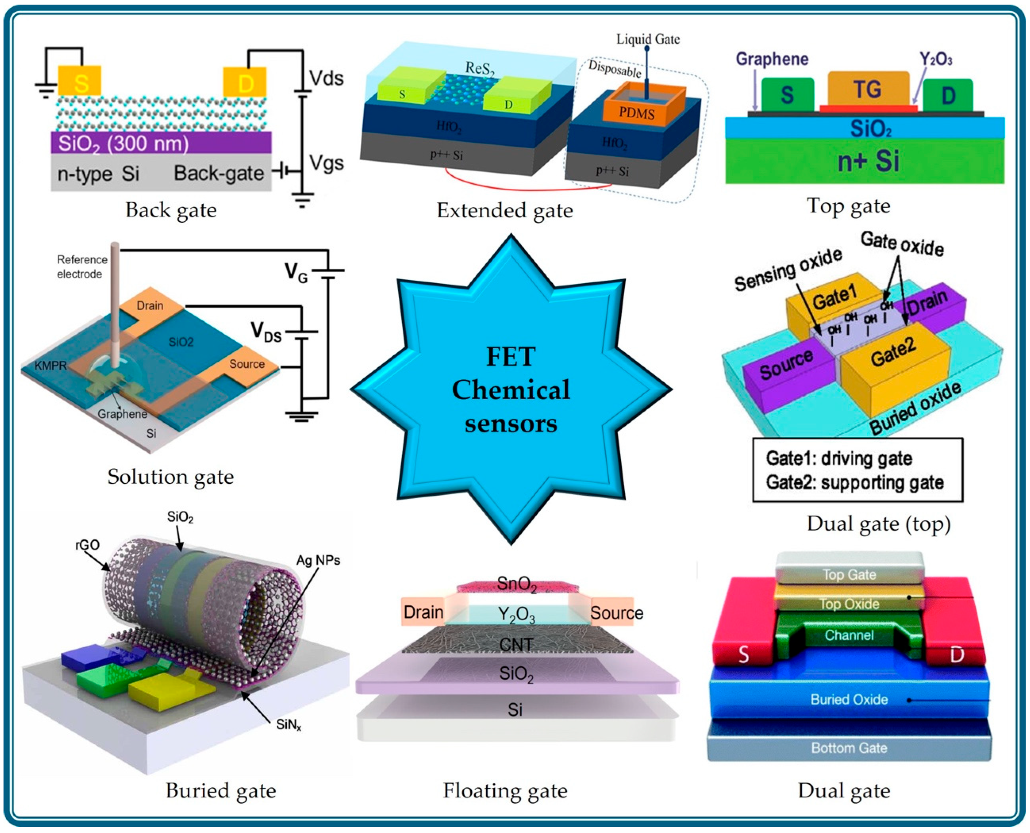
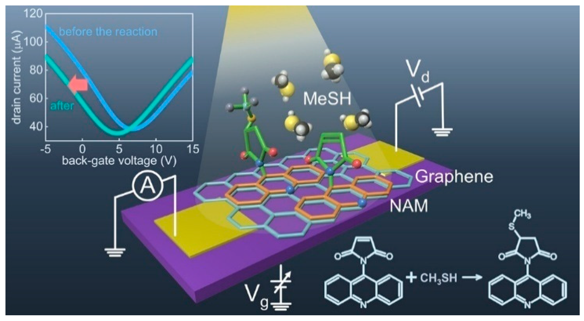
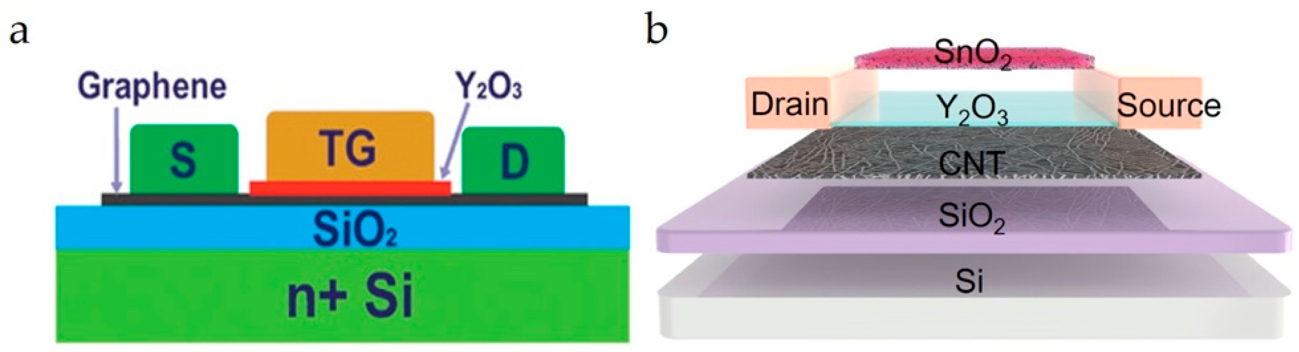
3. Bottom-Gate FET Chemical Sensor

The bottom-gate configuration is the most common in FET chemical sensors, employing an electric field to control the channel material’s electrical conductivity. In BG-FETs, the gate, comprising a dielectric and an electrode, lies beneath the semiconductor channel [10,43,44]. Typically, a heavily doped silicon substrate serves as both the substrate and the gate electrode.

3.1. History and Evaluation

Research into FET devices for chemical sensing began decades ago, with metal oxides commonly used as the active sensing layer (the channel). The first electronic nose was developed in 1982 [45]. The bottom-gate configuration has been the most studied and robust for modulating channel conductivity via an external electric field. Exposure to analytes influences channel conductivity secondarily, enabling target analyte detection.
The emergence of low-dimensional materials, particularly 2D materials, such as graphene, TMDs, and MXenes, has led to significant advancements in FET chemical sensors. Graphene is an excellent candidate for bottom-gate FET chemical sensors due to its chemical inertness, large effective surface area, and sensitivity to surface chemical perturbations. Further studies utilizing other 2D materials, such as MoS2, SnS2, BP, and PdSe2, have enhanced the chemical sensing performance in terms of sensitivity, selectivity, response/recovery times, and LOD. Their long-term stability and reliability were enhanced by employing the encapsulation techniques, which protect the active sensing layers from degradation during chemical interactions with the analytes. Furthermore, the integration of BG-FET chemical sensors with CMOS circuits offers miniaturization and low-power chemical sensing.

3.2. Working Principle

BG-FET chemical sensors operate by recording changes in the electrical properties of the channel upon interaction with the target analytes [10,43,46]. The sensing mechanism can be explained as follows. BG-FET chemical sensors utilize a channel material, such as graphene or a 2D layered material, whose electrical conductivity is modulated by both the adsorbed analytes and the applied back-gate voltage. The analyte adsorption induces charge transfer or electrostatic gating, altering the carrier density and/or mobility in the channel. This, in turn, modulates the channel’s current or conductance, which serves as the sensing signal. The back-gate bias influences the channel’s baseline carrier concentration, which can significantly amplify the sensor’s sensitivity and response to the target analyte. Changes in parameters such as the Dirac point or threshold voltage are monitored. Figure 2 schematically represents the sensing process in a BG-FET chemical sensor for methanethiol (MeSH) detection. The key aspects of BG-FET sensing mechanisms are as follows.

3.2.1. Charge Transfer

Analyte molecules can act as electron donors or acceptors, undergoing charge transfer interactions with semiconductor channel materials. Such interactions alter the channel’s carrier density, thus affecting its conductivity and shifting its Fermi level [10,43,47]. For example, the adsorption of an electron-accepting gas, such as NO2, on n-type semiconducting channels, such as MoS2 and SnS2, leads to a decrease in electron concentration and an increase in resistance [10,44]. Conversely, electron-donating gases, such as NH3, increase the electron concentration in n-type channels upon interaction, thereby decreasing resistance [10].

3.2.2. Electrostatic Gating Effect

The adsorbed analyte molecules, particularly if polar or charged, can create a local electric field that adds to the applied gate voltage and modulates channel conductance [48].

3.2.3. Scattering Effect

The adsorbed analyte molecules can act as scattering centers for charge carriers in the channel, reducing the mobility and affecting the overall conductance of the channel. This effect is significant for non-ionic adsorption of analytes [49].

3.2.4. Chemical Reactions

In some cases, analyte molecules undergo chemical reactions with the channel material. Such interactions lead to changes in the electronic structure and transport properties of channels. For example, during formaldehyde sensing with a SnS2 channel, oxygen atoms from formaldehyde fill the sulfur vacancies in the SnS2 lattice, leading to a p-type doping effect [44].

3.2.5. Quantum Capacitance Effect

In graphene-based devices, changes in the local chemical environment can affect the quantum capacitance of graphene, which, in turn, modulates the overall capacitance of graphene FET chemical sensor devices [50].

3.2.6. Schottky Barrier Modulation
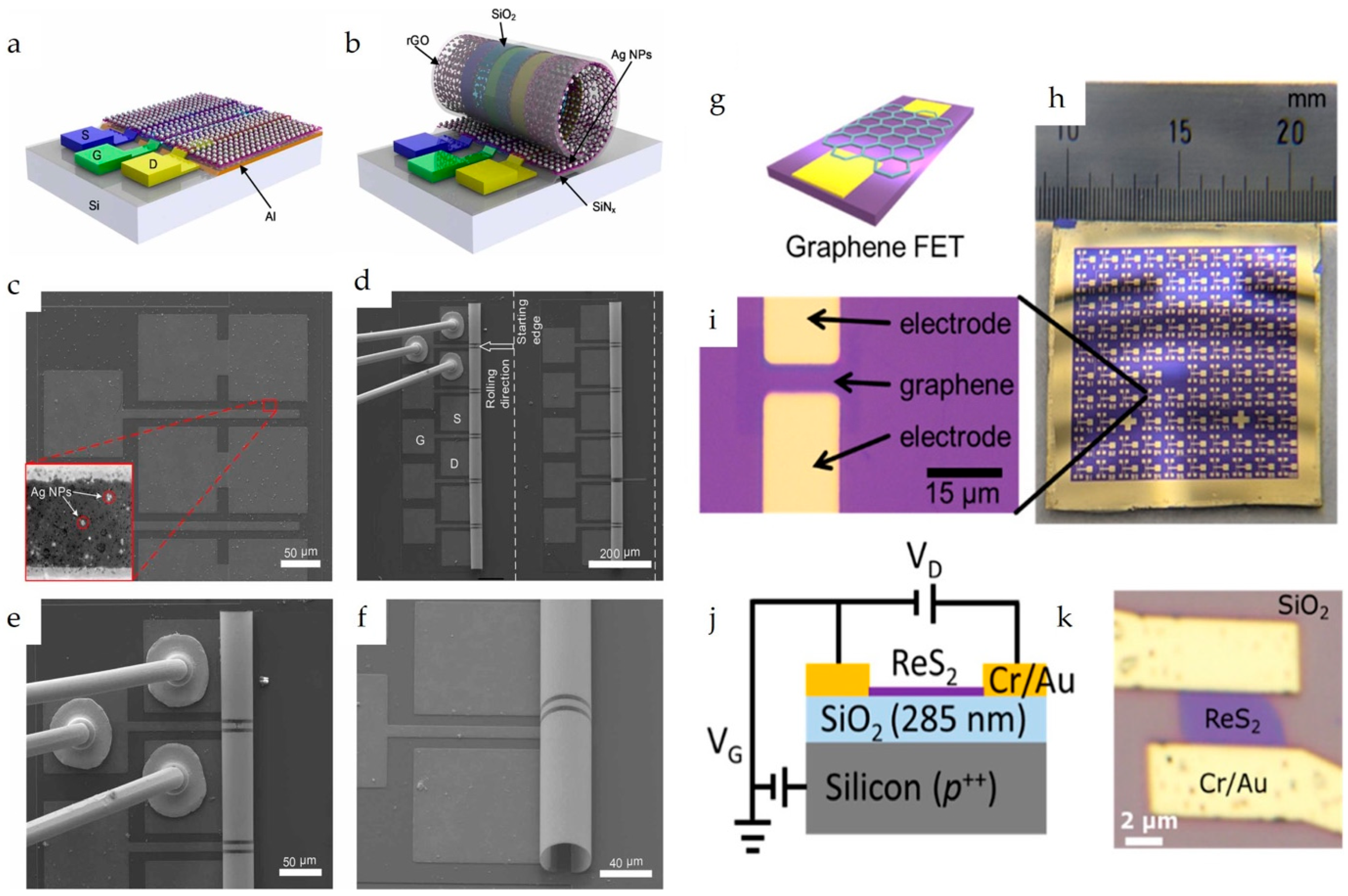
In FET chemical sensors with Schottky contacts between the semiconductor channel and metal electrodes, the adsorption of analyte molecules can alter the work function of the channel near the electrode contacts, thereby modifying the Schottky barrier height and influencing current flow [10].
It is important to note that the choice of the bottom-gate voltage plays a crucial role in the sensing performance. By applying specific bottom-gate voltages, the operating point of the sensor can be tuned to enhance its sensitivity to specific analytes [10,48,51]. For instance, operating a graphene FET chemical sensing device near its Dirac point can amplify the relative change in conductance upon gas adsorption, owing to the minimal carrier density at the Dirac point [51]. Similarly, applying a suitable gate voltage to an n-type MoS2 FET can either enhance or suppress its response to an electron-accepting gas such as NO2 by controlling the electron concentration in the channel [10].

3.3. Fabrication

The fabrication of bottom-gate FET chemical sensors involves conventional fabrication processes, such as substrate preparation with a gate dielectric, channel material deposition/transfer, electrode patterning and deposition, and in some cases, surface decoration or functionalization.

3.3.1. Substrate and Gate Dielectric

In most cases (except for flexible sensor devices), a heavily doped silicon substrate is used, covered with a gate dielectric such as thermally grown SiO2 or physically deposited HfO2, which acts as a gate insulator [10,43,44]. Few studies reported the use of AlOx as an insulating gate oxide on aluminum bottom gates [50].

3.3.2. Channel Material Deposition/Transfer

In general, 2D channel materials are either grown via chemical vapor deposition (CVD) [3,10] or exfoliated from bulk crystals or foils. Preferred exfoliation methods include scotch-tape-assisted mechanical and electrochemical exfoliation [49,52]. The 2D flakes are transferred to the target substrate using different techniques such as (i) dry transfer, (ii) polymer-assisted wet transfer [53], (iii) bubbling method [54], and (iv) thermal-release-tape-assisted transfer [49]. The 2D flakes prepared via chemical exfoliation methods require a solution-mediated deposition step, such as spin coating, drop casting, or printing. The choice of deposition or transfer method may require an additional channel-defining step, such as lithography/etching, to achieve the desired channel geometry [43].

3.3.3. Electrode Patterning and Deposition

Fabrication of source and drain electrodes involves a series of processes, such as forming a photoresist layer, patterning the photoresist layer by photo- or electron beam lithography, wet or dry etching of the photoresist to define the electrodes, deposition of electrodes by thermal/electron beam evaporation or sputtering, and finally, the lift-off process. The choice of electrode materials typically depends on the work function of the channel and material availability. Common electrode materials include gold, silver, platinum, and palladium. In some cases, a thin layer of chromium or titanium is used to enhance the adhesion of electrode materials to the channel [10,32,43,48,55].

3.3.4. Functionalization/Decoration

Surface modification of 2D channel materials, such as functionalization or decoration, has been employed to enhance the selectivity and/or sensitivity of FET sensing devices toward specific analytes. Reportedly, 2D channel materials are decorated with metal nanoparticles (e.g., silver and platinum) [38,56], metal–organic frameworks (MOFs) [10,57], single-stranded DNA (ssDNA) [3], and other sensing layers, such as molybdenum oxide (MoOx) or tin oxide (SnO2) [56,58]. Encapsulation layers such as aluminum oxide (Al2O3) can also be deposited to improve stability, particularly for materials sensitive to ambient conditions, such as BP [32].
Notably, an interesting approach in which a buried-gate FET chemical sensor is fabricated using MEMS technology has been reported [38]. This structure involved a sacrificial aluminum layer, strained silicon nitride layers, a Cr/Au gate electrode, an SiO2 gate dielectric, and a 3D Ag nanoparticle/reduced graphene oxide (rGO) microtubular sensing film (Figure 3a–f). In this case, the sacrificial Al layer was selectively etched after completing the device fabrication leading to the rolling up of the FET device and formation of the microtubular structure.

3.4. Advantages

The BG-FET sensor configuration is a common type of FET device, and these sensors possess most of the advantages of FET devices because their operation relies on changes in channel conductance caused by the external chemical environment. Key advantages of BG-FET chemical sensors are as follows:

3.4.1. High Sensitivity

FET devices are sensitive to changes in the electrical properties of their channel materials. The interaction of the channel material with the target analytes results in electronic changes in the channel material; therefore, the BG-FET sensors are highly sensitive. In addition, 2D channel materials offer better interactions with target analytes because of their high surface-to-volume ratios [10,50,58].

3.4.2. Tunable Sensitivity

The electrical properties (particularly, the channel conductance) of FET devices directly depend on the operational gate voltage. By tuning the gate voltage, the operational sensitivity of the BG-FET sensors can be tuned [48,51].

3.4.3. Low-Power Operation

The 2D-material-based BG-FET sensors can operate effectively at room temperature, eliminating the need for heating stages for high-temperature sensor operation, in contrast to the conventional metal-oxide-based sensors [44,58,59]. Furthermore, as electronic devices, their power requirements for sensing operations are significantly lower.

3.4.4. Potential for Miniaturization and Integration

The planar structure of BG-FETs makes them amenable to miniaturization and integration with microelectronic circuits, enabling the development of compact and portable sensing devices [10,38].

3.4.5. Versatility in Sensing Mechanism

BG-FETs can exploit changes in the resistance, capacitance, threshold voltage, carrier mobility, and Dirac point position for sensing, providing multiple parameters for monitoring [10,50].

3.5. Disadvantages

3.5.1. Stability Issues

FET-based sensors are inherently susceptible to environmental influences. BG-FET chemical sensors with 2D channel materials are sensitive to humidity and oxygen-group surface interactions, which can lead to sensor degradation over time. Encapsulation can effectively mitigate these stability issues [32].

3.5.2. Selectivity

Achieving high selectivity in BG-FET chemical sensors can be challenging because discriminating and understanding the sensing response of analytes with similar interfering compounds is difficult. Strategies such as functionalization, choice of gate voltage, and fabrication of an array of sensors with different sensing materials are useful for achieving selectivity toward the target analyte [3,10,60].

3.5.3. Hysteresis and Drift

Some BG-FET sensors exhibit hysteresis in their electrical characteristics (owing to the electrical characteristics of the channel material) and a drift in the baseline signal. This eventually affects the accuracy and reliability of the sensor measurements [10,60].

3.5.4. Contact Resistance

The electrical contact between the metal electrodes and the semiconductor channel significantly influences the device performance of BG-FET sensors. A high or unstable contact resistance can limit sensitivity and introduce noise into the measured signal [38].

3.5.5. Recovery Time

In some cases, the recovery of the sensor to its baseline state after exposure to the analyte can be slow, which limits the speed of the actual measurements [58].

3.6. Applications

BG-FET chemical sensors are widely used for detecting various species including inorganic gases, volatile organic compounds (VOCs), and organic molecules. The ultra-sensitive detection of methanethiol (MeSH) was reported by Sakamoto et al. [4] using a graphene channel BG-FET chemical sensor (Figure 3g–i), with a detection limit of 10 parts per billion (ppb). For highly selective detection, the graphene channel was functionalized with N-(9-Acridinyl)maleimide (NAM), which undergoes a chemical reaction upon MeSH exposure. This surface chemical reaction modulates the electrical characteristics of the graphene channels. Zulkefli et al. developed a BG-FET sensor using ReS2 for VOC detection (Figure 3j,k) [17]. Illumination of the channel material at different wavelengths modulates the sensing response to VOCs, such as acetone, methanol, and ethanol. Erande et al. fabricated a BG-FET sensor for humidity sensing using electrochemically exfoliated BP nanosheets as the channel material [33]. A similar BP-channel BG-FET humidity sensor was also reported by Miao et al., in which the stability of the channel material was improved using a 6-nm-thick Al2O3 coating [32].
Ju et al. reported capacitive sensing of nitrogen dioxide (NO2) based on the quantum capacitance effect [50]. An aluminum BG-FET chemical sensor was used, with graphene as the channel material. A 56% increase in the total capacitance was observed in the presence of 100 parts per million (ppm) NO2. Yin et al. constructed a 3D microtubular FET device using an rGO channel decorated with silver nanoparticles [38]. The reported sensor detected 20 ppm NO2 with a recovery time of 116 s. Cadore et al. reported the construction and testing of BG-FET sensors for ammonia gas sensing [52]. The BG-FETs were constructed using a graphene channel and different gate dielectrics, such as SiO2, talc, and hBN. The BG-FET with the hBN gate dielectric performed well in detecting ammonia gas, exhibiting a faster recovery and better electrical response.
Nozaki et al. constructed BG-FETs with ssDNA-modified graphene channels for ethanol detection [3]. Depending on the sequence of the functionalized ssDNA, ultra-low LODs of 1.5 ppb and 60 parts per trillion (ppt) for ethanol gas have been reported. Kybert et al. reported the construction of ssDNA-functionalized graphene channel BG-FET arrays for chemical vapor sensing [54]. A few-layer PdSe2 thin film on a silicon structure was used to construct a BG-FET chemical sensor for NO2 gas detection [34]. The sensing performance of BG-FETs with different PdSe2 film thicknesses was investigated, and an LOD of 0.1 ppm was reported for the 8 nm PdSe2 thin film device, as the best-performing device.
Wang et al. fabricated BG-FET sensors with an MoS2 channel for ammonia (NH3) detection and reported a 22-fold increase in sensitivity upon decoration of the MoS2 channel with FDM-23 (Cu6(m-BDC)6(H2O)6.H3[P(W3O10)4]) MOF [10]. Kumar et al. reported an MOF (Cu2(BDC)2SURMOF-2)-functionalized graphene channel BG-FET for the detection of VOCs, such as methanol, ethanol, and isopropanol [57]. Zong et al. fabricated a single-atom Pt (Pt SA)-implanted Ti3C2Tx MXene-channel BG-FET sensor and reported the detection of triethylamine (VOC) with an LOD of 14 ppb [61]. A strategy for decorating Ag nanoparticles on a Ti3C2Tx MXene channel was reported by Xu et al. for a BG-FET H2S sensor with an LOD of 35 ppb [62].
Azizi et al. fabricated a BG-FET chemical sensor with a monolayer Re0.5Nb0.5S2 channel for selective NO2 gas sensing and reported a good responsivity (~32% for 1 ppm of NO2) [63]. Gakhar et al. reported the role of a suitable gate voltage in enhancing the ethanol-sensing performance of a p-type TiO2-embedded GO channel BG-FET chemical sensor [51]. Falak et al. fabricated a BG-FET chemical sensor with a defined TiO2/graphene channel, in which the TiO2 coverage on graphene varied from 0 to 100% (0, 25, 50, 75, and 100%) [43]. The fabricated sensors exhibited an improved sensing performance with full recovery of NH3 gas through p- to n- mode switching by tuning the gate bias. In a similar report, the authors used thin MoOx layers to cover a predefined graphene channel and investigated the effect of the coverage area (0%, 25%, 50%, 75%, and 100%) on NH3 gas sensing [58].
An ultra-low LOD of ∼0.4 ppb for NO2 gas was reported by Xu et al. using a PtS2 BG-FET, along with sensitivity enhancement under UV light (405 nm) irradiation [64]. Majd et al. fabricated a DNA-carbon-dot-functionalized MoS2 BG-FET chemical sensor for targeted Hg2+ detection in water samples and reported an LOD of 1 aM [55]. In another study, a BG-FET sensor was developed using Ti3C2Tx MXene-channel material for the detection of Hg2+ ions in a high-salinity environment [65]. A Ti3C2Tx MXene-channel BG-FET was also reported for Ag+ ion detection, with an LOD of 0.28 μM [66].
Non-covalent functionalization of a graphene channel with 5-(4-hydroxyphenyl)-10,15,20-tri(p-tolyl)zinc porphyrin (ZnTTPOH) in a BG-FET chemical sensor has been reported for the gas-phase detection of 2,4,6-trinitrotoluene [53]. Hayashi et al. fabricated a BG-FET with a 2D SnS2 channel and reported the selective detection of formaldehyde (HCHO) with an LOD of ∼1 ppb [44]. Im et al. fabricated a similar MoS2 channel-based BG-FET sensor (Figure 4a–d) for NO2 gas detection [31]. An Al2O3 passivation layer was used to prevent an increase in the off current, which was realized because of the interaction of NO2 gas with the MoS2 channel. In another study, Al2O3 was used to protect the rGO channel in a BG-FET phosphate-ion sensor [67]. In this case, a recognition unit (horse ferritin) for phosphate ions was decorated on the Al2O3 passivation layer using a linker unit (cysteamine and glutaraldehyde). The reported BG-FET sensor can detect phosphate ions in water samples at up to 105 nM (LOD). A monolayer MoS2 BG-FET (Figure 4e–h) was fabricated and tested for NO2 gas sensing by Tabata et al. [49]. Under photoactivation, the fabricated sensor recorded good sensing performances with an LOD of ∼0.15 ppb against the NO2 gas. Table 1 provides a comparison of BG-FET sensors based on channel materials, analytes, and key sensing parameters.

4. Solution-Gate FET Chemical Sensors

The solution-gate FET (SG-FET) chemical sensor, also known as ion-sensitive FET (ISFET), is a specialized FET for sensing applications where the conventional solid gate is replaced by a liquid electrolyte solution containing an immersed reference or gate electrode. The semiconductor channel of an SG-FET is in contact with the electrolyte either directly or via a gate insulator layer [23,68,69].

4.1. History and Evaluation

The concept of field-effect sensing in the solution was pioneered by Bergveld in the early 1970s with the invention of the ISFET [70]. This pioneering work demonstrated the possibility of detecting ions in an electrolyte solution by monitoring the source-to-drain current (IDS) of an FET device where the metal gate was replaced by a reference electrode in contact with both the analyte-containing electrolyte solution and a gate insulator. The initial ISFET was designed and used to detect Na+ and H+ (pH values). Subsequently, the integration of newly developed nanomaterials improved the sensing characteristics of SG-FETs.
Early challenges in the field included sensor drift, limited selectivity, and the influence of Debye screening length in high-ionic-strength solutions. Since its discovery in 2004, graphene has emerged as an ideal candidate for SG-FET chemical sensors due to its outstanding electrical sensitivity to chemical environment changes and its chemical robustness [71,72]. The incorporation of other 2D materials, such as TMDs and MXenes, has also led to considerable improvements in SG-FET sensing characteristics.
Over the years, the development of analyte-selective membranes incorporating ionophores, the use of receptors such as aptamers and enzymes, and the integration of microfluidic systems have significantly enhanced the performance and applicability of SG-FET chemical sensors.

4.2. Working Principle

SG-FET chemical sensors operate based on the modulation of the electrical conductivity of the semiconductor channel. A gate voltage is applied through an electric double layer (EDL) formed in the electrolyte solution. When a target analyte interacts with the sensor surface (either the channel or the gate functionalization), it causes a change in the surface potential or charge distribution at the electrolyte/channel interface. This alteration, in turn, modifies the carrier density within the channel, leading to a measurable change in the channel’s electrical conductance or current. Figure 5 shows the construction and sensing operation of an SG-FET sensor featuring a COF/graphene channel (a representative example). The key aspects of the sensing mechanism of SG-FETs are as follows.

4.2.1. Electric Double-Layer (EDL) Formation

When a gate voltage is applied via the reference/gate electrode immersed in the electrolyte, ions within the electrolyte redistribute to screen the applied electric field at the solid–liquid interface [19,23,69]. This redistribution forms two oppositely charged layers, an ionic layer in the electrolyte and an electronic layer in the channel material. Separated by a very thin region (a few nanometers in width), these two layers are known as electric double layers (EDLs). The EDL effectively acts as a nanoscale capacitor, allowing strong electric fields to be induced in the channel at low gate voltages [69].

4.2.2. Electrostatic Gating Effect

The electric field generated by the EDL affects the carrier concentration (electrons or holes) in the channel material. A positive gate voltage attracts electrons (for n-type channels) or repels holes (for p-type channels), thereby increasing channel conductance. Conversely, a negative gate voltage depletes the electrons or accumulates holes, thereby decreasing conductance [68].

4.2.3. Analyte-Induced Surface Potential Changes

When a target analyte directly interacts with the sensing interface by binding to aptamers, ionophores, functional groups on the channel material surface, or a coating layer, it induces a change in the surface potential of the channel material or the gate oxide. This change in the surface potential influences changes in the threshold voltage (Vth or Dirac point for the graphene channel), leading to modulation of the channel current (IDS) for the same gate voltage [21,68,73,74,75].

4.2.4. Debye Screening

In electrolyte solutions, the electric field from the charged species is screened by the surrounding ions, and the characteristic distance of this screening is known as the Debye length (λD). For effective sensing, particularly for larger charged species such as biomolecules, the binding event should ideally occur within the Debye layer such that the charge changes are not completely screened from influencing the channel conductance [71].

4.3. Fabrication

The fabrication of SG-FET chemical sensors involves conventional fabrication steps (discussed in Section 3.3), with additional functionalization and cavity/sample holder construction.

4.3.1. Surface Functionalization

Surface functionalization is widely employed in SG-FETs to provide selectivity for target analytes. Depending on the target analyte and the specific sensor design, this functionalization involves either direct modification of the channel material itself or application of a selective layer or membrane on the sensing gate electrode or directly over the channel. Different recognition units and their functionalization strategies are discussed below.
Aptamers like DNA are immobilized on the graphene channel via covalent bonding. These aptamers exhibit high affinity for As(III) and K+, and upon such interaction with the target analyte, they cause changes in the surface charge distribution and changes in the EDL [28,76]. This will result in the detection of target analytes.
Ion-imprinted polymers (IIPs) are synthetic polymers engineered to have specific recognition sites that match the size and/or shape of target ions. Grafting IIPs onto materials like reduced graphene oxide (rGO) creates sensors where the selective binding of target ions, such as cadmium(II) (Cd(II)), induces a significant change in the resistance of the rGO channel [75].
Ion-selective membranes, known as ionophores, are the organic molecules that can selectively bind to specific ions. These ionophores are incorporated into ion-selective membranes (ISMs) to improve the selectivity of FET chemical sensors. For example, valinomycin is highly selective for potassium (K+). When the ISM is used as a sensing layer, the selective trapping of ions by the ionophore modulates the surface potential, which, in turn, controls the conductance of the FET channel. In some cases, complexation between ions and ionophores within the membrane can reduce ion mobility, increasing membrane impedance and affecting the voltage applied to the FET gate [22,60,77].
COFs are crystalline mesoporous polymers that have predesigned structures and nanopores. They can encapsulate and protect the sensing channel from fouling while providing a large surface area with specific sites for analyte receptors. COFs have been employed as sensing interfaces, for instance, on graphene, for sensitive and antifouling detection of targets like mercury(II) (Hg2+) by enabling selective absorption into their pores [23].
Materials such as Nafion can act as molecular sieves on the sensing interface, selectively allowing target analytes to reach the channel while blocking larger interfering molecules. For example, Nafion-coated graphene selectively detects protons (H+) for pH sensing by allowing them to pass through to reach the sensing layer [78].
CQDs functionalized with surface groups, such as carboxyl or hydroxyl, exhibit high selective affinity for specific ions such as cobalt(II) (Co(II)), iron(III) (Fe(III)), and copper(II) (Cu(II)). The interaction between these groups and the target ions (e.g., complexation with Fe(III) or coordination with Cu(II)) alters the capacitance of the EDL near the functionalized gate electrode, thereby modulating the channel current [79,80,81]. Similarly, ligands such as L-phenylalanine can also be functionalized on graphene, utilizing their amine and carboxylic groups to coordinate with metal ions (e.g., Na+, Co2+, Al3+, Cu2+), thus promoting interaction through π–π bonds with graphene [82]. Thiacalix [4]arene (TCA) immobilized on graphene allows for selective Cu(II) detection based on coordination with sulfur atoms, as explained by the hard and soft acids and bases (HSAB) theory [74].

4.3.2. Cavity/Sample Holder Construction

To contain the liquid electrolyte and sample, a sample holder consisting of a cavity or microfluidic channel is constructed around the sensing area. The sample cavity is often a simple, well-like structure composed of polydimethylsiloxane (PDMS) or silicone rubber [73,83]. The use of hydrophobic coatings such as CYTOP® inside the cavity has been reported to confine the sample droplets within the cavity structure. Microfluidic channels made of PDMS are aligned with the sensing channel to enable controlled flow of the liquid samples [84].

4.4. Advantages

SG-FETs offer several advantages over other FET chemical sensors. The following points are particularly noteworthy.

4.4.1. High Sensitivity

SG-FETs are highly sensitive to changes in the chemical environment, enabling the detection of smaller amounts (ppb) of analyte molecules. This sensitivity stems from the effective capacitive coupling of the analytes via a thin EDL, which enables strong modulation of the channel conductance, even with minor changes in the surface charge induced by analyte interactions [23,68,71].

4.4.2. Low-Voltage Operation

The high capacitance of the EDL enables these sensors to operate at low voltages (often below 1 V), which is favorable for portable devices and biological applications [69,84].

4.4.3. Label-Free Detection

SG-FET chemical sensors are highly sensitive devices that do not require fluorescent or enzymatic labels for target analytes [23,71,85].
Similar to other FET-type chemical sensors, SG-FETs also offer several other advantages, including real-time monitoring, potential for miniaturization and integration, and versatility in analyte detection.

4.5. Disadvantages

Some challenges associated with SG-FET chemical sensors that require careful consideration are discussed below.

4.5.1. Stability Issues (Drift)

Baseline drift is attributed to several factors, such as ion diffusion, electrochemical reactions, and temperature fluctuations, which can affect the accuracy and reliability of measurements [7,83].

4.5.2. Selectivity

Achieving high selectivity in SG-FETs can be challenging, particularly for complex samples containing multiple interferents. Owing to the highly sensitive nature of SG-FETs, a small amount of interference can disturb the measurements and results. Furthermore, non-specific binding of other molecules or ions to the sensing surface can lead to false positives [60].

4.5.3. Electrolyte Dependence

The performance of an SG-FET sensor is directly influenced by the electrolyte solution’s composition, pH, and ionic strength of the electrolyte solution. Therefore, careful consideration must be given to electrolyte selection to ensure its quality [73,76].

4.5.4. Debye Screening Limitation

Debye screening can limit the sensitivity of SG-FET sensors for detecting larger and/or charged biomolecules, particularly in high-ionic-strength solutions such as physiological buffers [71,85]. There are two widely used strategies for suppressing or eliminating the Debye screening effect. The first one is nanogap engineering, in which nanochannels or nanopores are used to confine the ionic solution [7,27]. This will alter the Debye length locally, thereby enhancing the sensitivity. The second one involves engineering or choosing smaller aptamer recognition units with lengths less than 2–3 nm, which ensures that the target binding events occur within the Debye screening length [33,68]. In addition, the ionic strength reduction can also increase the Debye screening length and improve the electrical coupling between the analytes and the sensing layer.

4.5.5. Potential for Electrochemical Reactions

During the sensing operation of SG-FETs, applying gate voltages to an electrolyte can lead to unwanted electrochemical reactions at the electrode–electrolyte interface, which can degrade sensor performance or introduce noise [68].

4.6. Applications

Wang et al. constructed a large-area monolayer graphene channel SG-FET and investigated its sensing properties [20]. Variations in the Dirac point of the graphene channel were observed upon exposure to different pH values and KCl solutions. Inaba et al. developed an SG-FET chemical sensor for ammonia gas sensing [69]. In the reported sensor, CVD-grown graphene was used as the channel material, and an ionic liquid (1-ethyl-3-methylimidazolium tetrafluoroborate ([EMIM][BF4])), was used as the solution gate. Interestingly, this ionic liquid absorbed NH3 gas when exposed to it and modulated its electrical properties by creating an EDL. The limit of detection (LOD) and response time were 130 ppb and 33 s, respectively. In another report, diethylmethyl (2-methoxyethyl)ammoniumbis(trifluoromethylsulfonyl)imide (DEMETFSI) ionic liquid was utilized as a gate in a graphene-channel SG-FET sensor for pH sensing and demonstrated a detection resolution of 2 × 10⁻⁴ [86]. Yang et al. (Figure 5) reported an SG-FET chemical sensor with antifouling sensing capabilities for Hg2+ ions [23]. The graphene channel was covered with a covalent organic framework (COF) based on tris(4-aminophenyl)benzene (TAPB) and 2,5-bis(methylthio)terephthalaldehyde (BMTTPA). The COF blocked fouling molecules (interferants) from interacting with the graphene channel. This strategy enables the selective detection of 10−10 M Hg2+ within 50 ms.
Ren et al. fabricated an SG-FET chemical sensor using a carbon-dot-sensitized graphene channel and reported selective detection of cobalt(II) (Co2+) ions with an LOD of 10−19 M [79]. Hu et al. constructed an SG-FET with an ion-imprinted polymer (IIP)-functionalized rGO channel for selective detection of cadmium (II) ions [75]. The IIP was developed through surface-initiated reversible addition-fragmentation chain transfer polymerization of polyethylenimine (PEI) and methacrylic acid monomers with Cd(II) ions as the template. This IIP enabled selective recognition of Cd(II) ions in water samples with an LOD of 0.83 ppb.
Wang et al. reported a graphene-channel SG-FET chemical sensor for As(III) detection in which ssDNA was used as the recognition unit for As(III) ions [76]. In contrast to other reports, ssDNA functionalization was performed on an Au gate electrode (in contrast to conventional channel functionalization). The ssDNA-functionalized Au gate was then treated with BSA to prevent the unfunctionalized Au surface from interacting with the ions in the solution. This suppressed interference effects and enabled the specific detection of As(III) ions with an LOD of 5 nM.
Employing a similar functionalization strategy, Fan et al. reported a graphene-channel SG-FET for Cu2+ sensing [80]. The Au gate electrode was functionalized with carbon quantum dots (QDs) using mercaptoacetic acid. The LOD for Cu2+ was recorded as 1 × 10⁻¹⁴ M. The same sensing system was also applied for the Fe3+ detection. Yao et al. also reported the functionalization of the Au gate electrode of an SG-FET with N-doped carbon decorated with a single Fe-site enzyme (Fe-N-C SAE) for the selective detection of Hg2+ ions [87]. Tu et al. fabricated an SG-FET sensor array with a graphene channel to selectively detect Hg2+ [71]. The channel material was functionalized with ssDNA, which served as a recognition unit for Hg2+ ions. The reported sensor was highly selective toward Hg2+, with an LOD of 40 pM.
Li et al. reported a graphene-channel SG-FET sensor with an ion-selective valinomycin-based membrane coated on top of the channel material [22]. The sensor was fabricated as a strip that could be directly dipped into an analyte-containing solution to selectively detect potassium (K+) ions. In another study, Gao et al. fabricated and investigated a graphene-channel SG-FET sensor for real-time pH monitoring of seawater [73]. Alves et al. detected multiple ions (Na+, Co2+, Al3+, and Cu2+) using a graphene-channel SG-FET via ion-selective l-phenylalanine functionalization [82]. Kim et al. constructed a multi-ion-responsive SG-FET chemical sensor using zinc oxide (ZnO) nanoglobules with GO and rGO as channel materials. The fabricated sensor exhibited a good response to Cr(III) and Cu(II) ions [88].
Wang et al. functionalized a graphene channel with an enzyme cascade reaction (ECR) system in an SG-FET chemical sensor to detect organophosphorus pesticides (OPs) [89]. The ECR system consists of acetylcholinesterase (AChE), a copper MOF of 1,3,5-benzenetricarboxylic acid (CuBTC), and CdS QDs. When OPs come into contact with these molecules, a series of light-activated catalytic reactions modulate the gating effect, resulting in a detectable variation in the device characteristics. These SG-FETs can detect OPs with an LOD of 0.5 pm.
Fakih et al. reported the real-time monitoring and simultaneous concentration measurement of K+, Na+, NH4+, NO3, SO42−, HPO42−, and Cl ions using a graphene-channel SG-FET array combined with Nikolsky–Eisenman analysis [60]. This method was employed to calculate the concentrations of individual ions in a multi-interference ion environment. Takagiri et al. immobilized thiacalix [4]arene (TCA) molecules on the graphene channel of an SG-FET for selective detection of Cu2+ ions [74]. Kim et al. (Figure 6a) reported the use of a nitrate-ion-selective membrane in a graphene-channel SG-FET for selective detection of nitrate ions in water [21]. Yuan et al. (Figure 6b–d) reported an enhancement in the K+ ion detection sensitivity of a graphene-channel SG-FET via plasma treatment (10 s), and the LOD reached 0.058 pM [28]. Lee et al. fabricated an SG-FET integrated with a microfluidic flow channel for the detection of H+ ions (pH) and glucose molecules [78]. The graphene channel layer was modified with Nafion coating and Au decoration to improve the sensing performance. Table 2 provides a comparison of SG-FET sensors based on channel materials, analytes, and key sensing parameters.

5. Extended-Gate FET Chemical Sensors

The EG-FET is an interesting sensor configuration where the sensing probe/element is physically separated from the FET transducer but electrically connected to its gate terminal [40]. This unique design retains the basic functionality of the metal–oxide–semiconductor FET (MOSFET) structure while incorporating an extended sensing element to the metal gate. The sensing element comprises a conductive layer, a sensing layer, an analyte solution holder, and an external reference electrode. The conductive layer acts as an extended gate electrode, while the sensing layer interacts with the target analyte.

5.1. History and Evaluation

Classical SG-FETs face packaging and sensitivity issues due to the direct contact of the FET structure with the analyte (i.e., solution gate). To overcome these drawbacks, Van der Spiegel proposed an EG-FET in 1983 [90]. The proposed EG-FET configuration features a sensing element spatially separated from the actual FET transducer. This physical separation of the sensing elements increases the design flexibility of EG-FET sensors. This separation also helps to overcome the stability-related drawbacks of SG-FETs, offering the potential for long-term stability.

5.2. Working Principle

The working mechanism of an EG-FET involves analyte recognition by the extended-gate (EG) sensing element and the signal transduction by the physically separated Field-Effect Transistor (FET) transducer. The EG surface, functionalized with a sensing layer, directly interacts with the target analyte in the sample. This interaction causes a change in the electrical surface potential of the EG. This potential change is then electrically transmitted to the gate of the FET. The FET, acting as a transducer, converts this gate voltage shift into a measurable electrical signal, typically a change in its drain current [40,91,92]. Figure 7a,b schematically represents the pH sensing operation in EG-FET chemical sensor. The interaction between the extended sensing part and the target analyte is governed by either one or a combination of the following mechanisms.

5.2.1. Ion/Analyte Molecule Binding

During sensing, the target analyte that comes into contact with the sensing layer binds to it, influencing a change in the surface potential. This change in the surface potential modulates the gate voltage of the transducer and the resultant electrical characteristics [24,26,77].

5.2.2. Electrochemical/Chemical Reactions

Electrochemical and chemical reactions of analytes occurring during the sensing process can generate or consume charged species, leading to changes in the surface potential. For example, enzyme-based FET sensors utilize enzymatic reactions that produce ions, which are then detected by EG-FET sensors [93,94].

5.3. Fabrication

The fabrication of EG-FET chemical sensors followed the processes described in Section 3.3, with additional extended-gate fabrication. The fabrication of an extended gate resembled that of an FET device, but without source and drain electrodes. The extended gate is constructed by depositing a sensing layer (e.g., 2D materials and metal oxides) on a conductive substrate (usually a heavily doped silicon or a glass/PET substrate with a metal/conducting layer) [26,27]. The substrate is electrically connected to the transducer FET gate. The sensing layer is coated with ionophore layers or target-specific functional molecules for the detection of specific analytes such as metal ions and biomolecules [77]. A sample chamber was optionally constructed (shown in Figure 7a) to analyze liquid analytes similar to solution gating with an additional reference electrode [26,95].

Surface Functionalization

The surface functionalization strategies used in EG-FETs to improve the selectivity are similar to those of SG-FET chemical sensors (Section 4.3.1). A few examples are discussed as follows: (i) An ionophore-embedded polymer membrane can be used to detect specific metal ions. For example, a cadmium ionophore embedded in a PVC membrane was used to selectively detect Cd2+ ions in human serum [77]. This membrane acts as a filter, allowing only the target Cd2+ ion to pass through. The interaction between cadmium ions and the ionophore within the membrane leads to a change in the membrane’s impedance, particularly the real part (resistance), which causes a detectable voltage drop applied to the FET. (ii) Metal oxides can be used to detect pH, as they can selectively interact with H+ ions. As examples, SnO2 [24], Al2O3 [27], and HfO2 [26] layers were used for pH sensing. These materials have hydroxyl groups on their surface that can reversibly bind to hydronium ions, causing a change in surface potential.

5.4. Advantages

EG-FET chemical sensors offer unique advantages over other FET configurations, due to their structural differences. The key advantages are as follows.

5.4.1. Design Flexibility

The spatial separation of the extended gate, i.e., the sensing part, from the transducer FET allows for the use of different sensing layers, geometries, and processing methods, particularly those unsuitable for the construction of a conventional FET structure [40,95]. Additionally, EG-FETs can be adapted to a wide range of analytes, including ions and small molecules, by modifying the sensing layer [40].

5.4.2. Protection of the Transducer and Reusability

The FET transducer is physically separated from the sensor, and therefore, it can be protected from harsh sample exposure and other environmental conditions (such as temperature and light). This improves the long-term stability of FET transducers [24]. The FET transducer can be reused if the sensing component is designed as a disposable element. This helps to reduce production costs by replacing the entire sensing unit.

5.5. Disadvantages

While issues such as the drift and instability of the output signal, the requirement of an external reference electrode (as in the case of SG-FETs), and the complexity of fabrication are common in FET sensors, EG-FET chemical sensors have some notable disadvantages that arise because of their configurational difference.

5.5.1. Drop in Sensitivity

As discussed earlier, the extended sensing gate is physically separated and connected through an electrical connection line. This can result in signal loss and decreased sensitivity during actual measurements [96,97].

5.5.2. Larger Device Footprint

The physical separation of the extended gate part combined with the FET transducer unit results in a larger device footprint compared to other integrated FET sensors.

5.6. Applications

Liao et al. constructed an EG-FET chemical sensor (Figure 7a,b) using a layered ReS2 channel material for pH sensing [26]. The extended gate was constructed by depositing HfO2 on a heavily doped Si substrate with a PDMS solution cavity on top. A notable LOD of 0.0132 pH (e.g., it can detect the difference between 2.0 and 2.02 pH) was reported, with a sensitivity of 54.8 mV/pH.
Wei et al. fabricated an EG-FET (Figure 7c–e) on a glass substrate [27]. The transducer consisted of an MoS2/graphene channel and an hBN gate dielectric. The sensing component was constructed on a glass substrate using graphene as the conducting layer and a stacked hBN/Al2O3 as the ion-selective membrane for pH sensing. The reported LOD was 1.54 × 10⁻³ pH and the sensitivity was 166 mV/pH. In another study, a similar EG-FET was reported using only hBN as the pH sensing layer [95].

6. Dual-Gate FET Chemical Sensors

The DG-FET sensor is an FET device with two gates: one positioned at the bottom and the other at the top of the channel material. Both gates are separated from the channel material using a gate oxide. The second gate enables better control over transistor characteristics, particularly the threshold voltage, which can be adjusted by applying a potential to it.

6.1. History and Evaluation

Dual-gate thin-film transistors (TFTs) were first reported in 1981, using CdSe as the semiconductor channel material. The development of TFT technologies, such as amorphous silicon and organic semiconductors, has led to further development of DG-FETs. Initially, the primary focus of DG-FETs was their application in logic gates and integrated circuits, where the tunability of the threshold voltage offered advantages in circuit performance [98,99].
Over time, DG-FETs have been used for sensing. The first demonstration of ISFETs was a breakthrough in FET chemical sensors due to their wide applicability and large current change in response to small shifts in the threshold voltage [70]. However, the low sensitivity of ISFETs is a limitation, particularly for biomolecule- and label-free sensing applications. To improve sensitivity in the above-mentioned cases, the concept of a dual gate was employed, that is, ISFETs were constructed with a DG-FET structure. The underlying principle for sensitivity enhancement is the capacitive coupling between the two gate dielectrics, which can amplify small changes in the surface potential. This amplification varies linearly with the capacitive coupling [100,101,102]. DG-FET chemical sensors fabricated using 2D channel materials, such as graphene and MoS2, outperformed conventional silicon-based devices in sensitivity and noise-limited resolution [86].

6.2. Working Principle

Similar to other FET sensing devices, the change in the surface potential due to the interaction with target analytes or analyte-associated reactions modulates the channel conductance, which is the primary working principle. In DG-FETs, one gate can be used to set the operating point of the transistor, whereas the other responds to the target analyte, leading to a change in electrical characteristics. Figure 8 illustrates the operation of a DG-FET chemical sensor.

6.2.1. Amplification Through Capacitive Coupling

The dual-gate configuration can amplify changes in the surface potential. The potential change induced in one gate is capacitively coupled with that in the other gate through the semiconducting channel and dielectric layers. This capacitive coupling leads to a shift in the threshold voltage at one gate, caused by a change in the surface potential at the other gate. The magnitude of this shift is proportional to the capacitance ratio of the two gate dielectrics [98,103]. By optimizing these capacitance values, the sensitivity to analyte-induced changes in surface potential can be enhanced.

6.2.2. Dielectric and Work Function Modulation

For detecting gases and biomolecules such as DNA, dielectric modulation and work-function modulation have been reported for dual-gate graphene nanoribbon FETs. During dielectric modulation, the presence of analyte molecules near the gate dielectric changes the local dielectric constant, thereby altering the electrical characteristics of the DG-FET sensor. In work function modulation, the adsorption of gas molecules onto a catalytic metal or conducting polymer gate can alter the work function of the gate, leading to a change in channel conductance [104].

6.2.3. Charge Trapping

In asymmetrical DG-FETs, the top gate (In2Se3) acts as a charge-trapping layer and enables non-volatile memory. The trapping and detrapping of charges in this layer modulate the channel conductance and form the basis for memory and sensing applications in a single device [99].

6.3. Fabrication

The fabrication of DG-FETs is similar to that of BG-FETs, with additional gate fabrication. As discussed in Section 3.3, heavily doped Si was used as the substrate, which also served as the back gate. Thermally grown SiO2 or other oxides, such as HfO2 or AlOx served as the dielectric layer for the back gate. The 2D channel materials were then transferred to or deposited onto SiO2. Subsequently, an additional dielectric layer was deposited (by physical vapor deposition) or transferred (mechanically exfoliated layered materials such as hBN) over the channel material, serving as the gate dielectric for the top gate. A gate electrode was deposited on top of the second dielectric layer in the desired pattern using a shadow mask or photolithography-based pre-patterning. The sensing layer was functionalized or decorated with specific recognition molecules to improve the selectivity of DG-FET sensors. For ISFET operations requiring liquid analyte, a sample holder chamber or flow channel was constructed using PDMS or similar polymers.

6.4. Advantages

The primary advantage of DG-FETs is their higher sensitivity compared to single-gate FET sensors. Capacitive coupling between the two gates amplifies the signal and improves sensitivity. The other advantages include the following.

6.4.1. Tunable Threshold Voltage

The presence of the second gate enables dynamic tunability of the threshold voltage, which is beneficial for optimizing the operating point and sensitivity for the target analyte [98].

6.4.2. Versatile Functionality

The dual-gate structure enables multifunctional devices to integrate logic, memory, and sensing capabilities into a single architecture [99].

6.4.3. Improved Electrical Characteristics

The dual-gate configuration can yield improved device characteristics such as a high on/off ratio and a lower subthreshold swing [99].

6.4.4. Improved Sensing Performances

In addition to improved sensitivity and tunable threshold voltage, DG-FET sensors possess additional sensing advantages, such as a higher signal-to-noise ratio and faster response times [103].

6.5. Applications

Lee et al. reported dual-gate operation in an FET sensor fabricated with an EG-FET-type physical structure, that is, the transducer and sensing parts were fabricated separately and interconnected. An enhanced sensitivity of 2085.53 mV/pH was reported during the dual-gate mode sensing operation (as shown in Figure 8) [24].

7. Other Gate Configurations

Although not all gate configuration FETs strictly fall within the scope of 2D materials and chemical sensors, they are reviewed to understand the diversity in gate configurations.

7.1. Top-Gate FETs

The design of top-gate FETs (TGFETs) involves the deposition of a dielectric layer on top of a semiconducting channel. The dielectric layer can be an oxide (such as Hf2O3, Y2O3, or Al2O3), a nitride layer (such as hBN), or a polymer layer (such as PDMS) [35,105,106]. After depositing the gate dielectric layer, the top-gate electrode is defined by lithography patterning or a shadow mask, followed by electrode deposition. The thin top gate dielectric allows for better control over the channel conductance modulation, and therefore, better device performance can be achieved from TG-FETs (a representative schematic is shown in Figure 9a).

7.2. Floating-Gate FETs

Floating-gate FET (FG-FETs) sensors possess two gates, where one acts as the sensing gate and the other as the control gate. The floating gate is separated from the control gate and channel material using a dielectric layer. For example, Huang et al. fabricated an FG-FET sensor (Figure 9b) with a CNT channel material [37]. In this case, a Y2O3 layer was used to separate the SnO2 floating gate (sensing layer) from the channel. In another CNT-channel-based FG-FET sensor, a Pd-decorated WS2 floating gate was isolated using a Y2O3 layer [107]. In FG-FET sensors, the channel conductance is modulated by the potential difference between the floating gate and the channel. The amplification effect was also reported in FG-FETs, which helped to detect trace gases, with LOD down to ppb levels (20 ppb). Shi et al. fabricated an MoS2 channel FG-FET gas sensing device for NO2 analytes [25]. In this case, an hBN layer is deposited over the source/drain electrodes. Finally, a BP layer was deposited as the gas-recognition layer. The reported device structure was advantageous in that the BP layer and the hBN dielectric layer protected the device performance from NO2 gas poisoning and enabled easier recovery. The LOD for NO2 gas is 3.3 ppb.

8. Cross-Sensitivity

Different gate configurations in FET chemical sensors offer distinct advantages and mechanisms to handle cross-sensitivity and chemical interference. As discussed earlier in the manuscript, functionalization with analyte-specific recognition units improves selectivity in all gate configurations. Apart from functionalization, BG-FETs are reported to use different gate voltages [10] and illumination at specific wavelengths (650 nm for acetone) to recognize specific gas analytes [17].
In EG-FETs, the sensing gate is separated from the transducer, and therefore, this gate configuration is well-suited for fabricating multi-species microprobes. EG-FETs fabricated with multiple sensing gates, functionalized with different target-specific recognition units, can be used as an array to respond selectively to a specific analyte [90].
In SG-FETs, a blocking layer is used to hinder the non-specific interaction of chemical interferents. For example, in an SG-FET sensor, the Au gate electrode was functionalized with ssDNA served as the recognition unit for As(III) ions. In this report, an additional functionalization step was carried out using BSA molecules in order to block non-specific interactions of other chemical species with the gate electrode [76].
In DG-FETs, different biases can be applied simultaneously, which helps to tune the gating effect and dominant sensing mechanism (gate potential-dependent). This strategy is used to improve selectivity in gas sensing using DG-FETs [16]. In addition, DG-FETs are reportedly advantageous in biological environments and samples with high salt contents. The Debye screening length is a major limiting factor in such sample environments, and DG-FETs help to mitigate this issue [24].

9. Stability and Lifetime

Stability and lifetime are critical aspects for the real-world application of FET-based chemical sensors, including those using Bottom-Gated (BG), Extended-Gate (EG), and Solution-Gated (SG) configurations. Different gate designs and the materials used for the channel and sensing layers significantly influence these properties.
The stability of BG-FETs can vary depending on the channel materials and passivation layers. In general, the widely used graphene channel is more stable compared to other channel materials. The use of metal oxide layers (a 6 nm-thick Al2O3) enhanced the stability of few-layer black phosphorus (BP) devices, preventing them from degrading completely in just four days under ambient conditions [32]. A similar Al2O3 passivation layer improved the on-off switching responses of an MoS2 channel BG-FET sensor reported for NO2 sensing, yielding stable and clean signals [31]. MoOx decoration on the graphene channel also improved sensing performance, demonstrating good stability for around 5 months [58].
Stability in SG-FETs is significantly influenced by the channel material, electrolyte, and functionalization/decoration. SG-FETs fabricated with ZnO-NGs@GO and ZnO-NGs@rGO hybrid channel material survived stability tests over 40 consecutive days, showing only a minor reduction in sensor response for Cr(III) and Cu(II) detection [88]. Graphene channel SG-FETs with a valinomycin ion-selective membrane for K+ detection showed excellent repeatability and reliability in sensing experiments conducted over two months [22]. The performance remained unchanged when tested in Tris-HCl solution or when fabricated on a PET substrate. Another graphene channel SG-FET with an ionic liquid gate maintained device stability and performance over several months when kept under high vacuum [86].
The EG architecture itself offers advantages for stability and packaging because it decouples the FET transducer from the chemically sensitive region. The stability of EG-FET chemical sensors is heavily influenced by the material used for the extended gate sensing layer. An EG-FET chemical sensor with a graphene/hBN sensing gate exhibited stability in drain current over 5200 s, with a drift value ~0.50 mV/hour [95]. This low drift is attributed to the hBN sensing gate’s good diffusion barrier against ions. Similarly, an EG-FET with an Al2O3/hBN sensing gate also demonstrated good stability with a reasonable drift value of 4 mV/hr and better pH resolution [27].

10. Power Requirements

The power requirements, particularly the operational voltage range, are a critical consideration when assessing the suitability of different FET gate configurations for wearable devices, which typically rely on low-power, battery operation. The power requirements for Back-Gated (BG), Extended-Gate (EG), and Solution-Gated (SG) FETs, in the context of wearable applications, are discussed as follows:

10.1. Back-Gated (BG) FETs

Conventional BG-FETs, particularly those using a thick silicon dioxide (SiO2) layer as the gate insulator, often require high gate voltages, typically several tens of volts. For instance, an rGO channel BG-FET was reported with an operational gate voltage range from −40 to 40 V [67]. While some BG configurations use lower gate voltage ranges (e.g., −10 to 10 V for Re0.5Nb0.5S2 FETs [63], −5 to 15 V for graphene FETs [4], or −10, −5, +5, +10 V for MoS2/FDM-23 FETs [10]), the need for substantial bottom-gate voltages in many designs is highlighted as a critical problem when applying these devices to low-power and low-voltage sensor devices, such as battery-powered, energy-harvesting, and CMOS-integrated sensors. The drain-source voltage (Vds) in BG-FETs can be relatively low, with examples at ~0.1 V, 50 mV, 1 V, or 5 V [10,63,67]. However, the high gate voltage requirement is often the limiting factor for low-power wearable use.

10.2. Solution-Gated (SG) FETs

SG-FETs use an electrolyte and a gate electrode immersed in it to modulate the channel conductance. This configuration is particularly common for sensing in liquids. A major advantage highlighted for SG-FETs, especially those using ionic liquids (ILs), is their ability to operate at low voltages. Ionic liquids can form a very thin electric double layer (around 1 nm) at the gate interface, allowing for effective gating with much lower voltages compared to solid dielectric layers like thick SiO2. Examples of operational voltage ranges observed in SG-FETs include: (i) Gate voltage (Vg) from −0.8 to 0.8 V using an ionic liquid for gas sensing [69]. (ii) Gate voltage (Vg) from −0.1 to 0.3 V with Vds from −50 to 50 mV for pH sensing in PBS solution [73]. (iii) Gate voltage (Vg) sweep from −0.8 V to 2.2 V with a drain bias of 0.5 V for K+ detection [28]. (iv) Gate voltage (Vg) sweep from −0.8 to 2.0 V with Vds from 0 to 0.8 V for SG-FET arrays for the detection of Hg2+ [71]. These low operating voltage ranges (typically within a few volts) make SG-FETs, especially IL-gated variants, well-suited for low-power, battery-operated devices, aligning with the requirements for wearable applications. While promising for low-voltage operation and high sensitivity, challenges remain for ionic liquid-gated graphene FETs regarding achieving a robust device structure with scalable and sensor-compatible fabrication processes and high process yields for commercial viability, which are practical considerations for widespread wearable use.

10.3. Extended-Gate (EG) FETs

EG-FETs are generally advantageous for low-power wearable sensing applications. However, achieving high sensitivity frequently involves operating the FET transducer in the subthreshold regime. This necessitates measuring low current levels (commonly in the nA range) and requires broad potential sweeping ranges (typically larger than 10 V) [40]. These conditions are not compatible with conventional portable readout electronics, which operate within typical ranges of voltage less than ~10 V and current from ~10 μA to ~10 mA. Operating the FET in the saturation region is better suited for portable applications as it involves larger values of drain current and is more easily interfaced with portable electronics. Developing EG-FET systems compatible with these portable voltage/current ranges is key for wearable integration. Portable EG-FET platforms have been demonstrated [108,109]. Therefore, compared to BG-FETs, both SG-FETs (particularly those using ionic liquids) and EG-FETs are promising due to their ability to operate at significantly lower voltages (within a few volts or even 1 V or below).

11. Summary and Outlook

Field-effect transistor (FET) chemical sensors have evolved as a promising sensing platform for detecting various chemical species due to their strong sensitivity and potential for integration with amplifying circuits at the micron scale. This review paper presents the classification of 2D FET chemical sensors based on their gate configurations. There are four major gate configurations, such as back-gate (BG-FETs), solution-gate (SG-FETs), extended-gate (EG-FETs), and dual-gate (DG-FETs), each with distinct characteristics that determine their suitability for specific sensing applications.

11.1. Comparative Analysis of Gate Configurations

Table 3 provides a comparison of different gate configurations in key aspects. In BG-FETs, the gate is positioned beneath the semiconducting channel. BG-FET chemical sensors with 2D channel materials offer the advantages of simpler fabrication and miniaturization potential. The sensing mechanism in BG-FETs includes charge transfer, electrostatic gating, and scattering effects. Thick dielectric layers (typically 90–300 nm SiO2) result in higher operating voltages (5–20 V) but provide excellent environmental isolation, contributing to device longevity. BG-FETs demonstrate notable efficacy for the detection of reducing gases (NH3) and oxidizing gases (NO2) with 2D materials like graphene, showing detection limits down to 0.1 ppb for NO2.
SG-FETs employ a liquid gate, which enables the detection of ions and molecules in the liquid environment. Despite having advantages like high sensitivity and low-power operation, SG-FETs struggle to achieve selectivity and often require functionalization with specific recognition units. The electrical double layer formation at the semiconductor-solution interface results in high gate capacitance (10–100 pF), allowing for operation at significantly lower voltages (0.5–3 V). This configuration has shown exceptional performance in biosensing applications, with MoS2-based SG-FETs demonstrating protein detection at sub-picomolar concentrations.
EG-FETs have a spatially separated gate (sensing part), which is electrically connected to the back gate of the FET transducer. The EG-FET configuration offers long-term stability of the transducer but suffers from sensitivity loss due to gate separation. This physically separated gate configuration makes EG-FETs particularly suitable for harsh environments and long-term monitoring applications. The reduced interference between the sensing and transducing components allows for greater flexibility in substrate choice and device architecture.
DG-FETs have two independent gates positioned at the top and bottom of the channel material. The dual gate operation provides enhanced control over the channel conductance and amplifies signals through capacitive coupling. However, it accompanies fabrication and operational complexities. The unique ability of DG-FETs to modulate channel properties through two independent gates enables superior discrimination in complex media with multiple interfering species, with demonstrated capacity to distinguish between structurally similar volatile organic compounds (VOCs).

11.2. Thematic Analysis of FET Chemical Sensor Applications

Throughout all the configurations, the use of 2D channel materials improved the device sensitivity, selectivity, and detection limits. Three primary sensing themes have emerged across the various gate configurations:

11.2.1. Environmental Monitoring

FET chemical sensors have demonstrated significant efficacy in ambient air quality monitoring. BG-FETs with graphene channels show exceptional sensitivity to NO2 (0.1 ppb) and NH3 (1 ppb), while MoS2-based DG-FETs enable selective detection of VOCs in complex mixtures. For environmental pollutants in water, SG-FETs functionalized with specific recognition elements have achieved detection limits for heavy metal ions in the sub-ppb range, with Pb2+ detection demonstrated at 0.5 ppb using graphene oxide channels.

11.2.2. Healthcare and Biomedical Applications

The integration of biorecognition elements with different gate configurations has enabled highly specific biosensing platforms. SG-FETs excel in this domain, with protein detection limits reaching picomolar concentrations. The EG-FET configuration has proven particularly valuable for point-of-care diagnostics due to its enhanced stability and compatibility with complex biological matrices. Graphene and MoS2 channel materials functionalized with antibodies have demonstrated the detection of cardiac biomarkers (troponin, BNP) at clinically relevant concentrations (0.1–1 ng/mL).

11.2.3. Industrial Safety and Process Monitoring

The robust nature of BG-FETs makes them suitable for industrial environments, while the enhanced discrimination capabilities of DG-FETs enable selective detection in complex industrial atmospheres. EG-FETs with appropriate encapsulation have demonstrated operational stability in high-temperature and high-humidity environments for periods exceeding two years, making them suitable for continuous industrial process monitoring.
It is observed that modifications like functionalization with recognition units, DNA, metal nanoparticles, or organic molecules further improve selectivity and sensitivity. In parallel, challenges like device stability over time, selectivity among interfering species, environmental noise, and reproducibility of the fabrication process remain on a case-by-case basis.

11.3. Emerging Hybrid Gate Configurations

Recent advances have led to the development of hybrid gate architectures that combine the advantages of multiple configurations. (i) Floating-Extended Gates: Combining floating gate principles with extended gate architecture to enhance capacitive coupling while maintaining transducer protection. (ii) Reconfigurable Dual-Gates: Systems capable of switching between back-gate and solution-gate operation modes depending on the target analyte and environment. (iii) Vertically Stacked Heterojunction Gates: Leveraging the unique band alignments of different 2D materials to create gate structures with inherent selectivity towards specific analyte categories. These hybrid approaches represent a promising direction for overcoming the inherent limitations of individual gate configurations.

11.4. Future Outlook

Extensive research efforts are needed to overcome existing challenges. For example, the development of efficient passivation layers can increase the lifetime of the sensors. Engineering new 2D heterostructures can enable tunable device characteristics. Creating an array of FET sensors with different functionalization can enable multimodal detection.
Future research directions should focus on the following:
  • Material Engineering: Development of defect-engineered 2D materials with tailored sensing properties, exploration of vertical and lateral heterostructures to create built-in p-n junctions that enhance gate efficiency.
  • Gate Dielectric Innovation: Investigation of high-κ dielectrics for back-gate configurations to reduce the operating voltage while maintaining sensitivity; development of ion-selective solid-state electrolytes for solution-gate devices to improve stability.
  • System-Level Integration: Advancement of multi-sensor arrays with different gate configurations on a single chip to enable comprehensive analyte profiling; integration of on-chip reference sensors for drift compensation and environmental variability correction.
  • Standardization Efforts: Development of standardized testing protocols to enable a meaningful comparison between different gate configurations; establishment of benchmark performance metrics specific to each application domain.
Furthermore, coupling FET sensors with machine learning and deep learning approaches can complement the sensor performance by recognizing complex signal patterns. Applying these strategies can improve the real-world applicability of the FET sensors. Integration of FET sensors with secondary circuits, for example, fabricating a sensor with an amplifying circuit in a single chip, can further boost its practical usability.
In conclusion, the field of FET chemical sensors has gained substantial advancements through innovations in gate architecture, with each configuration offering distinct operational benefits tailored to specific sensing environments and analyte classes. The bottom-gate configuration provides robust performance for gas sensing, the solution-gate excels in biomolecular detection, the extended-gate offers superior stability in harsh conditions, and the dual-gate enables enhanced discrimination in complex mixtures. Nonetheless, challenges such as selectivity, environmental stability, and fabrication complexity persist. Notably, the integration with CMOS-compatible platforms, the exploration of novel two-dimensional materials, and the development of multifunctional hybrid gate designs are influencing the future trajectory of this technology. Future research should prioritize scalable fabrication, real-time multi-analyte detection, and design standardization to ensure reproducibility. Gate engineering remains the most efficient strategy to optimize device performance and adaptability for investigation and integration across application domains such as healthcare, environmental monitoring, and industrial safety.

Author Contributions

G.B. conceptualization, data curation, validation, and writing—original draft; S.H. visualization and writing—review and editing. All authors have read and agreed to the published version of the manuscript.

Funding

This work was supported by a National Research Foundation of Korea (NRF) grant funded by the Korean government (MSIT) (No. RS-2023-0024456 and No. RS-2024-00445819).

Conflicts of Interest

The authors declare no conflicts of interest.

References

  1. Chen, X.; Liu, C.; Mao, S. Environmental Analysis with 2D Transition-Metal Dichalcogenide-Based Field-Effect Transistors. Nano-Micro Lett. 2020, 12, 95. [Google Scholar] [CrossRef] [PubMed]
  2. Dai, C.; Liu, Y.; Wei, D. Two-Dimensional Field-Effect Transistor Sensors: The Road toward Commercialization. Chem. Rev. 2022, 122, 10319–10392. [Google Scholar] [CrossRef] [PubMed]
  3. Nozaki, R.; Ikuta, T.; Ueno, K.; Tsukakoshi, K.; Ikebukuro, K.; Maehashi, K. Ethanol Detection at the Parts per Billion Level with Single-Stranded-DNA-Modified Graphene Field-Effect Transistors. Phys. Status Solidi B 2020, 257, 1900376. [Google Scholar] [CrossRef]
  4. Sakamoto, Y.; Ikuta, T.; Maehashi, K. Electrical Detection of Molecular Transformations Associated with Chemical Reactions Using Graphene Devices. ACS Appl. Mater. Interfaces 2021, 13, 45001–45007. [Google Scholar] [CrossRef]
  5. Khatib, M.; Haick, H. Sensors for Volatile Organic Compounds. ACS Nano 2022, 16, 7080–7115. [Google Scholar] [CrossRef]
  6. Anichini, C.; Czepa, W.; Pakulski, D.; Aliprandi, A.; Ciesielski, A.; Samorì, P. Chemical Sensing with 2D Materials. Chem. Soc. Rev. 2018, 47, 4860–4908. [Google Scholar] [CrossRef] [PubMed]
  7. Fan, Q.; Wang, L.; Xu, D.; Duo, Y.; Gao, J.; Zhang, L.; Wang, X.; Chen, X.; Li, J.; Zhang, H. Solution-Gated Transistors of Two-Dimensional Materials for Chemical and Biological Sensors: Status and Challenges. Nanoscale 2020, 12, 11364–11394. [Google Scholar] [CrossRef]
  8. Chen, S.; Sun, Y.; Fan, X.; Xu, Y.; Chen, S.; Zhang, X.; Man, B.; Yang, C.; Du, J. Review on Two-Dimensional Material-Based Field-Effect Transistor Biosensors: Accomplishments, Mechanisms, and Perspectives. J. Nanobiotechnol. 2023, 21, 144. [Google Scholar] [CrossRef]
  9. Mao, S.; Chang, J.; Pu, H.; Lu, G.; He, Q.; Zhang, H.; Chen, J. Two-Dimensional Nanomaterial-Based Field-Effect Transistors for Chemical and Biological Sensing. Chem. Soc. Rev. 2017, 46, 6872–6904. [Google Scholar] [CrossRef]
  10. Wang, B.; Li, H.; Tan, H.; Gu, Y.; Chen, L.; Ji, L.; Sun, Z.; Sun, Q.; Ding, S.; Zhang, D.W.; et al. Gate-Modulated High-Response Field-Effect Transistor-Type Gas Sensor Based on the MoS2 /Metal–Organic Framework Heterostructure. ACS Appl. Mater. Interfaces 2022, 14, 42356–42364. [Google Scholar] [CrossRef]
  11. Song, J.; Guo, T.; Huang, C.; Liu, M.; Cui, H.; Huang, W.; Wang, Y.; Li, T. Part per Trillion Level DMMP Gas Sensor Based on Calixarene Modified Organic Thin Film Transistor. Chem. Eng. J. 2022, 446, 137097. [Google Scholar] [CrossRef]
  12. Bian, L.; Wang, Z.; White, D.L.; Star, A. Machine Learning-Assisted Calibration of Hg2+ Sensors Based on Carbon Nanotube Field-Effect Transistors. Biosens. Bioelectron. 2021, 180, 113085. [Google Scholar] [CrossRef] [PubMed]
  13. Xu, Y.; Zhou, P.; Simon, T.; Cui, T. Ultra-Sensitive Nitrate-Ion Detection via Transconductance-Enhanced Graphene Ion-Sensitive Field-Effect Transistors. Microsyst. Nanoeng. 2024, 10, 137. [Google Scholar] [CrossRef] [PubMed]
  14. Zhang, J.; Liu, L.; Yang, Y.; Huang, Q.; Li, D.; Zeng, D. A Review on Two-Dimensional Materials for Chemiresistive- and FET-Type Gas Sensors. Phys. Chem. Chem. Phys. 2021, 23, 15420–15439. [Google Scholar] [CrossRef]
  15. Liu, C.; Ye, Z.; Wei, X.; Mao, S. Recent Advances in Field-effect Transistor Sensing Strategies for Fast and Highly Efficient Analysis of Heavy Metal Ions. Electrochem. Sci. Adv. 2022, 2, e2100137. [Google Scholar] [CrossRef]
  16. Zhang, P.; Xiao, Y.; Zhang, J.; Liu, B.; Ma, X.; Wang, Y. Highly Sensitive Gas Sensing Platforms Based on Field Effect Transistor-A Review. Anal. Chim. Acta 2021, 1172, 338575. [Google Scholar] [CrossRef] [PubMed]
  17. Zulkefli, A.; Mukherjee, B.; Sahara, R.; Hayakawa, R.; Iwasaki, T.; Wakayama, Y.; Nakaharai, S. Enhanced Selectivity in Volatile Organic Compound Gas Sensors Based on ReS2 -FETs under Light-Assisted and Gate-Bias Tunable Operation. ACS Appl. Mater. Interfaces 2021, 13, 43030–43038. [Google Scholar] [CrossRef]
  18. Chen, J.; Pu, H.; Hersam, M.C.; Westerhoff, P. Molecular Engineering of 2D Nanomaterial Field-Effect Transistor Sensors: Fundamentals and Translation across the Innovation Spectrum. Adv. Mater. 2022, 34, 2106975. [Google Scholar] [CrossRef]
  19. Hu, W.-P.; Yang, Y.-Q.; Lee, C.-H.; Vu, C.-A.; Chen, W.-Y. Comparing Solution-Gate and Bottom-Gate Nanowire Field-Effect Transistors on pH Sensing with Different Salt Concentrations and Surface Modifications. Talanta 2024, 271, 125731. [Google Scholar] [CrossRef]
  20. Yu Wang, Y.; Burke, P.J. A Large-Area and Contamination-Free Graphene Transistor for Liquid-Gated Sensing Applications. Appl. Phys. Lett. 2013, 103, 052103. [Google Scholar] [CrossRef]
  21. Kim, J.; Liu, Q.; Cui, T. Solution-Gated Nitrate Sensitive Field Effect Transistor with Hybrid Film: CVD Graphene/Polymer Selective Membrane. Org. Electron. 2020, 78, 105551. [Google Scholar] [CrossRef]
  22. Li, H.; Zhu, Y.; Islam, M.S.; Rahman, M.A.; Walsh, K.B.; Koley, G. Graphene Field Effect Transistors for Highly Sensitive and Selective Detection of K+ Ions. Sens. Actuators B Chem. 2017, 253, 759–765. [Google Scholar] [CrossRef]
  23. Yang, L.; Jin, Y.; Wang, X.; Yu, B.; Chen, R.; Zhang, C.; Zhao, Y.; Yu, Y.; Liu, Y.; Wei, D. Antifouling Field-Effect Transistor Sensing Interface Based on Covalent Organic Frameworks. Adv. Electron. Mater. 2020, 6, 1901169. [Google Scholar] [CrossRef]
  24. Lee, I.-K.; Jeun, M.; Jang, H.-J.; Cho, W.-J.; Lee, K.H. A Self-Amplified Transistor Immunosensor under Dual Gate Operation: Highly Sensitive Detection of Hepatitis B Surface Antigen. Nanoscale 2015, 7, 16789–16797. [Google Scholar] [CrossRef]
  25. Shi, S.; Hu, R.; Wu, E.; Li, Q.; Chen, X.; Guo, W.; Sun, C.; Hu, X.; Zhang, D.; Liu, J. Highly-Sensitive Gas Sensor Based on Two-Dimensional Material Field Effect Transistor. Nanotechnology 2018, 29, 435502. [Google Scholar] [CrossRef]
  26. Yuan, Q.; Wu, S.; Ye, C.; Liu, X.; Gao, J.; Cui, N.; Guo, P.; Lai, G.; Wei, Q.; Yang, M.; et al. Sensitivity Enhancement of Potassium Ion (K+) Detection Based on Graphene Field-Effect Transistors with Surface Plasma Pretreatment. Sens. Actuators B Chem. 2019, 285, 333–340. [Google Scholar] [CrossRef]
  27. Liao, W.; Wei, W.; Tong, Y.; Chim, W.K.; Zhu, C. Low-Frequency Noise in Layered ReS2 Field Effect Transistors on HfO2 and Its Application for pH Sensing. ACS Appl. Mater. Interfaces 2018, 10, 7248–7255. [Google Scholar] [CrossRef]
  28. Hong, S.; Wu, M.; Hong, Y.; Jeong, Y.; Jung, G.; Shin, W.; Park, J.; Kim, D.; Jang, D.; Lee, J.-H. FET-Type Gas Sensors: A Review. Sens. Actuators B Chem. 2021, 330, 129240. [Google Scholar] [CrossRef]
  29. Sulleiro, M.V.; Dominguez-Alfaro, A.; Alegret, N.; Silvestri, A.; Gómez, I.J. 2D Materials towards Sensing Technology: From Fundamentals to Applications. Sens. Bio-Sens. Res. 2022, 38, 100540. [Google Scholar] [CrossRef]
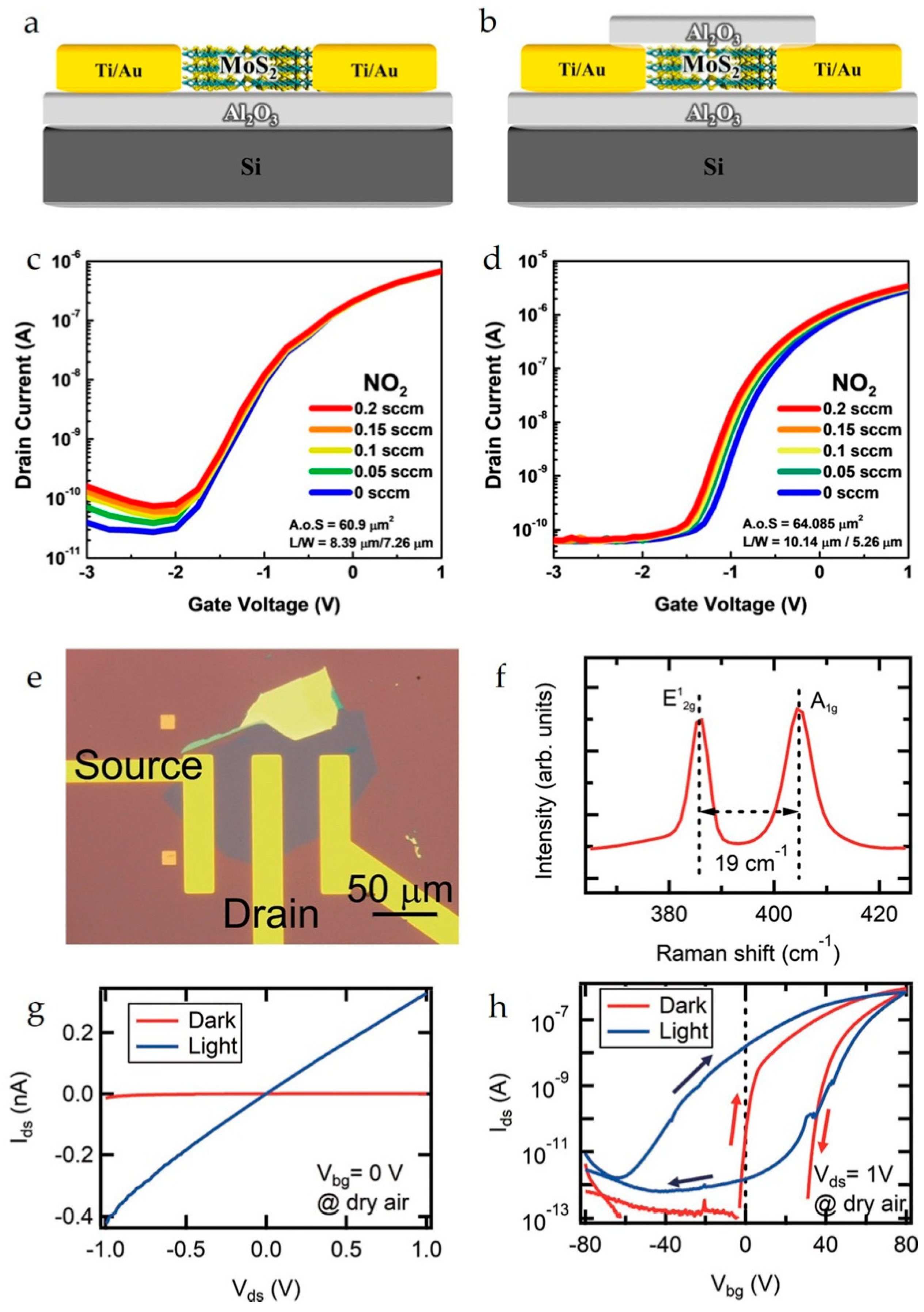
  30. Im, H.; AlMutairi, A.; Kim, S.; Sritharan, M.; Kim, S.; Yoon, Y. On MoS2 Thin-Film Transistor Design Consideration for a NO2 Gas Sensor. ACS Sens. 2019, 4, 2930–2936. [Google Scholar] [CrossRef]
  31. Miao, J.; Cai, L.; Zhang, S.; Nah, J.; Yeom, J.; Wang, C. Air-Stable Humidity Sensor Using Few-Layer Black Phosphorus. ACS Appl. Mater. Interfaces 2017, 9, 10019–10026. [Google Scholar] [CrossRef]
  32. Erande, M.B.; Pawar, M.S.; Late, D.J. Humidity Sensing and Photodetection Behavior of Electrochemically Exfoliated Atomically Thin-Layered Black Phosphorus Nanosheets. ACS Appl. Mater. Interfaces 2016, 8, 11548–11556. [Google Scholar] [CrossRef]
  33. Wei, W.; Zeng, Z.; Liao, W.; Chim, W.K.; Zhu, C. Extended Gate Ion-Sensitive Field-Effect Transistors Using Al2O3 /Hexagonal Boron Nitride Nanolayers for pH Sensing. ACS Appl. Nano Mater. 2020, 3, 403–408. [Google Scholar] [CrossRef]
  34. Fan, J.-L.; Hu, X.-F.; Fu, C.; Qin, W.-W.; Min, X.-J.; Zhao, J.-W.; Luo, L.-B.; Zhang, W. Few-Layer PdSe2 Nanofilm/Si Heterojunction for Sensing NO2 at Room Temperature. ACS Appl. Nano Mater. 2021, 4, 7358–7370. [Google Scholar] [CrossRef]
  35. Xu, H.; Zhang, Z.; Xu, H.; Wang, Z.; Wang, S.; Peng, L.-M. Top-Gated Graphene Field-Effect Transistors with High Normalized Transconductance and Designable Dirac Point Voltage. ACS Nano 2011, 5, 5031–5037. [Google Scholar] [CrossRef]
  36. Ahn, J.-H.; Kim, J.-Y.; Seol, M.-L.; Baek, D.J.; Guo, Z.; Kim, C.-H.; Choi, S.-J.; Choi, Y.-K. A pH Sensor with a Double-Gate Silicon Nanowire Field-Effect Transistor. Appl. Phys. Lett. 2013, 102, 083701. [Google Scholar] [CrossRef]
  37. Huang, Y.; Zhou, Y.; Liu, Y.; Chen, J.; Wei, X.; Cao, J. SnO2 /Carbon Nanotube Floating-Gate Field-Effect Transistor Gas Sensor for Ppb-Level CO Detection. ACS Appl. Nano Mater. 2024, 7, 16119–16126. [Google Scholar] [CrossRef]
  38. Yin, W.; Sun, J.; Zhang, Y.; Zhang, Y.; Li, S.; Zhu, M.; Hong, H.; Ba, Y.; Deng, T. A Novel Three-Dimensional Ag Nanoparticles/Reduced Graphene Oxide Microtubular Field Effect Transistor Sensor for NO2 Detections. Nanotechnology 2021, 32, 025304. [Google Scholar] [CrossRef]
  39. Mackin, C.; Fasoli, A.; Xue, M.; Lin, Y.; Adebiyi, A.; Bozano, L.; Palacios, T. Chemical Sensor Systems Based on 2D and Thin Film Materials. 2D Mater. 2020, 7, 022002. [Google Scholar] [CrossRef]
  40. Janićijević, Ž.; Nguyen-Le, T.-A.; Baraban, L. Extended-Gate Field-Effect Transistor Chemo- and Biosensors: State of the Art and Perspectives. Next Nanotechnol. 2023, 3–4, 100025. [Google Scholar] [CrossRef]
  41. Afsar, M.F.; Rafiq, M.A.; Jamil, A.; Fareed, S.; Siddique, F.; Tok, A.I.Y.; Hasan, M.M.U. Development of High-Performance Bismuth Sulfide Nanobelts Humidity Sensor and Effect of Humid Environment on Its Transport Properties. ACS Omega 2019, 4, 2030–2039. [Google Scholar] [CrossRef]
  42. Ali, S.; Kazmi, S.M.T.; Sher, F.; Nigah, A.; Bilal, M.; Rafiq, M.A. Fast, Sensitive, and Selective Hydrogen Sensing of Silver-Doped Bismuth Sulfide Nanobelts. J. Electron. Mater. 2024, 53, 2753–2762. [Google Scholar] [CrossRef]
  43. Falak, A.; Tian, Y.; Yan, L.; Zhang, X.; Xu, L.; Song, Z.; Dong, F.; Chen, P.; Zhao, M.; Wang, H.; et al. Simultaneous Achievement of Superior Response and Full Recovery of Titanium Dioxide/Graphene Hybrid FET Sensors for NH3 through p- to n-Mode Switch. Phys. Chem. Chem. Phys. 2020, 22, 16701–16711. [Google Scholar] [CrossRef]
  44. Hayashi, K.; Kataoka, M.; Jippo, H.; Ohfuchi, M.; Sato, S. Vacancy-Assisted Selective Detection of Low-Ppb Formaldehyde in Two-Dimensional Layered SnS2. ACS Appl. Mater. Interfaces 2020, 12, 12207–12214. [Google Scholar] [CrossRef] [PubMed]
  45. Persaud, K.; Dodd, G. Analysis of Discrimination Mechanisms in the Mammalian Olfactory System Using a Model Nose. Nature 1982, 299, 352–355. [Google Scholar] [CrossRef]
  46. Liu, Y.; Liu, Y.; Xiao, H.; Xiao, H.; Xiao, H.; Xiao, H.; Goddard, W.A.; Goddard, W.A. Schottky-Barrier-Free Contacts with Two-Dimensional Semiconductors by Surface-Engineered MXenes. J. Am. Chem. Soc. 2016, 138, 15853–15856. [Google Scholar] [CrossRef]
  47. Yan, W.; Lv, C.; Zhang, D.; Chen, Y.; Zhang, L.; Ó Coileáin, C.; Wang, Z.; Jiang, Z.; Hung, K.-M.; Chang, C.-R.; et al. Enhanced NO2 Sensitivity in Schottky-Contacted n-Type SnS2 Gas Sensors. ACS Appl. Mater. Interfaces 2020, 12, 26746–26754. [Google Scholar] [CrossRef] [PubMed]
  48. Tripathy, S.; Sett, A.; Majumder, S.; Bhattacharyya, T.K. Study of Gate Induced Sensitivity Amplification in Carbon Nanotube Thin Film Transistor Based Ammonia Sensor. Sens. Actuators B Chem. 2023, 382, 133511. [Google Scholar] [CrossRef]
  49. Tabata, H.; Matsuyama, H.; Goto, T.; Kubo, O.; Katayama, M. Visible-Light-Activated Response Originating from Carrier-Mobility Modulation of NO2 Gas Sensors Based on MoS2 Monolayers. ACS Nano 2021, 15, 2542–2553. [Google Scholar] [CrossRef]
  50. Ju, W.; Lee, S. Al Back-Gated Graphene Field-Effect Transistors for Capacitive Sensing Applications Based on Quantum Capacitance Effect. AIP Adv. 2022, 12, 095210. [Google Scholar] [CrossRef]
  51. Gakhar, T.; Hazra, A. P-TiO2/GO Heterojunction Based VOC Sensors: A New Approach to Amplify Sensitivity in FET Structure at Optimized Gate Voltage. Measurement 2021, 182, 109721. [Google Scholar] [CrossRef]
  52. Cadore, A.R.; Mania, E.; Alencar, A.B.; Rezende, N.P.; De Oliveira, S.; Watanabe, K.; Taniguchi, T.; Chacham, H.; Campos, L.C.; Lacerda, R.G. Enhancing the Response of NH3 Graphene-Sensors by Using Devices with Different Graphene-Substrate Distances. Sens. Actuators B Chem. 2018, 266, 438–446. [Google Scholar] [CrossRef]
  53. Gajarushi, A.S.; Surya, S.G.; Walawalkar, M.G.; Ravikanth, M.; Rao, V.R.; Subramaniam, C. Ultra-Sensitive Gas Phase Detection of 2,4,6-Trinitrotoluene by Non-Covalently Functionalized Graphene Field Effect Transistors. Analyst 2020, 145, 917–928. [Google Scholar] [CrossRef] [PubMed]
  54. Kybert, N.J.; Han, G.H.; Lerner, M.B.; Dattoli, E.N.; Esfandiar, A.; Charlie Johnson, A.T. Scalable Arrays of Chemical Vapor Sensors Based on DNA-Decorated Graphene. Nano Res. 2014, 7, 95–103. [Google Scholar] [CrossRef]
  55. Mansouri Majd, S.; Ghasemi, F.; Salimi, A.; Sham, T.-K. Transport Properties of a Molybdenum Disulfide and Carbon Dot Nanohybrid Transistor and Its Applications as a Hg2+ Aptasensor. ACS Appl. Electron. Mater. 2020, 2, 635–645. [Google Scholar] [CrossRef]
  56. Han, J.-W.; Rim, T.; Baek, C.-K.; Meyyappan, M. Chemical Gated Field Effect Transistor by Hybrid Integration of One-Dimensional Silicon Nanowire and Two-Dimensional Tin Oxide Thin Film for Low Power Gas Sensor. ACS Appl. Mater. Interfaces 2015, 7, 21263–21269. [Google Scholar] [CrossRef]
  57. Kumar, S.; Pramudya, Y.; Müller, K.; Chandresh, A.; Dehm, S.; Heidrich, S.; Fediai, A.; Parmar, D.; Perera, D.; Rommel, M.; et al. Sensing Molecules with Metal–Organic Framework Functionalized Graphene Transistors. Adv. Mater. 2021, 33, 2103316. [Google Scholar] [CrossRef]
  58. Falak, A.; Tian, Y.; Yan, L.; Xu, L.; Song, Z.; Hu, H.; Dong, F.; Adamu, B.I.; Zhao, M.; Chen, P.; et al. Ultrathin MoOx/Graphene Hybrid Field Effect Transistor Sensors Prepared Simply by a Shadow Mask Approach for Selective ppb-Level NH3 Sensing with Simultaneous Superior Response and Fast Recovery. Adv. Mater. Interfaces 2020, 7, 1902002. [Google Scholar] [CrossRef]
  59. Kim, Y.; Kang, S.-K.; Oh, N.-C.; Lee, H.-D.; Lee, S.-M.; Park, J.; Kim, H. Improved Sensitivity in Schottky Contacted Two-Dimensional MoS2 Gas Sensor. ACS Appl. Mater. Interfaces 2019, 11, 38902–38909. [Google Scholar] [CrossRef]
  60. Fakih, I.; Durnan, O.; Mahvash, F.; Napal, I.; Centeno, A.; Zurutuza, A.; Yargeau, V.; Szkopek, T. Selective Ion Sensing with High Resolution Large Area Graphene Field Effect Transistor Arrays. Nat. Commun. 2020, 11, 3226. [Google Scholar] [CrossRef]
  61. Zong, B.; Xu, Q.; Mao, S. Single-Atom Pt-Functionalized Ti3C2Tx Field-Effect Transistor for Volatile Organic Compound Gas Detection. ACS Sens. 2022, 7, 1874–1882. [Google Scholar] [CrossRef] [PubMed]
  62. Xu, Q.; Zong, B.; Li, Q.; Fang, X.; Mao, S.; Ostrikov, K. (Ken) H2S Sensing under Various Humidity Conditions with Ag Nanoparticle Functionalized Ti3C2Tx MXene Field-Effect Transistors. J. Hazard. Mater. 2022, 424, 127492. [Google Scholar] [CrossRef] [PubMed]
  63. Azizi, A.; Dogan, M.; Long, H.; Cain, J.D.; Lee, K.; Eskandari, R.; Varieschi, A.; Glazer, E.C.; Cohen, M.L.; Zettl, A. High-Performance Atomically-Thin Room-Temperature NO2 Sensor. Nano Lett. 2020, 20, 6120–6127. [Google Scholar] [CrossRef] [PubMed]
  64. Xu, H.; Huang, H.-P.; Fei, H.; Feng, J.; Fuh, H.-R.; Cho, J.; Choi, M.; Chen, Y.; Zhang, L.; Chen, D.; et al. Strategy for Fabricating Wafer-Scale Platinum Disulfide. ACS Appl. Mater. Interfaces 2019, 11, 8202–8209. [Google Scholar] [CrossRef]
  65. Hao, S.; Liu, C.; Chen, X.; Zong, B.; Wei, X.; Li, Q.; Qin, H.; Mao, S. Ti3C2Tx MXene Sensor for Rapid Hg2+ Analysis in High Salinity Environment. J. Hazard. Mater. 2021, 418, 126301. [Google Scholar] [CrossRef]
  66. Liu, C.; Wei, X.; Hao, S.; Zong, B.; Chen, X.; Li, Z.; Mao, S. Label-Free, Fast Response, and Simply Operated Silver Ion Detection with a Ti3C2TxMXene Field-Effect Transistor. Anal. Chem. 2021, 93, 8010–8018. [Google Scholar] [CrossRef]
  67. Zhou, G.; Jin, B.; Wang, Y.; Dong, Q.; Maity, A.; Chang, J.; Ren, R.; Pu, H.; Sui, X.; Mao, S.; et al. Ultrasensitive Sensors Based on Aluminum Oxide-Protected Reduced Graphene Oxide for Phosphate Ion Detection in Real Water. Mol. Syst. Des. Eng. 2020, 5, 936–942. [Google Scholar] [CrossRef]
  68. An, J.H.; Jang, J. A Highly Sensitive FET-Type Aptasensor Using Flower-like MoS2 Nanospheres for Real-Time Detection of Arsenic(III). Nanoscale 2017, 9, 7483–7492. [Google Scholar] [CrossRef]
  69. Inaba, A.; Yoo, K.; Takei, Y.; Matsumoto, K.; Shimoyama, I. Ammonia Gas Sensing Using a Graphene Field–Effect Transistor Gated by Ionic Liquid. Sens. Actuators B Chem. 2014, 195, 15–21. [Google Scholar] [CrossRef]
  70. Bergveld, P. Development, Operation, and Application of the Ion-Sensitive Field-Effect Transistor as a Tool for Electrophysiology. IEEE Trans. Biomed. Eng. 1972, BME-19, 342–351. [Google Scholar] [CrossRef]
  71. Tu, J.; Gan, Y.; Liang, T.; Hu, Q.; Wang, Q.; Ren, T.; Sun, Q.; Wan, H.; Wang, P. Graphene FET Array Biosensor Based on ssDNA Aptamer for Ultrasensitive Hg2+ Detection in Environmental Pollutants. Front. Chem. 2018, 6, 333. [Google Scholar] [CrossRef] [PubMed]
  72. Ang, P.K.; Chen, W.; Wee, A.T.S.; Loh, K.P. Solution-Gated Epitaxial Graphene as pH Sensor. J. Am. Chem. Soc. 2008, 130, 14392–14393. [Google Scholar] [CrossRef]
  73. Gao, J.; Wang, Y.; Han, Y.; Gao, Y.; Wang, C.; Han, L.; Zhang, Y. Graphene-Based Field-Effect Transistors Integrated with Microfluidic Chip for Real-Time pH Monitoring of Seawater. J. Mater. Sci. Mater. Electron. 2020, 31, 15372–15380. [Google Scholar] [CrossRef]
  74. Takagiri, Y.; Ikuta, T.; Maehashi, K. Selective Detection of Cu2+ Ions by Immobilizing Thiacalix[4]Arene on Graphene Field-Effect Transistors. ACS Omega 2020, 5, 877–881. [Google Scholar] [CrossRef] [PubMed]
  75. Hu, J.; Sedki, M.; Shen, Y.; Mulchandani, A.; Gao, G. Chemiresistor Sensor Based on Ion-Imprinted Polymer (IIP)-Functionalized rGO for Cd(II) Ions in Water. Sens. Actuators B Chem. 2021, 346, 130474. [Google Scholar] [CrossRef]
  76. Wang, Y.; Bi, Y.; Wang, R.; Wang, L.; Qu, H.; Zheng, L. DNA-Gated Graphene Field-Effect Transistors for Specific Detection of Arsenic(III) in Rice. J. Agric. Food Chem. 2021, 69, 1398–1404. [Google Scholar] [CrossRef]
  77. Wang, S.-L.; Hsieh, C.-Y.; Wu, C.-R.; Chen, J.-C.; Wang, Y.-L. Highly Sensitive FET Sensors for Cadmium Detection in One Drop of Human Serum with a Hand-Held Device and Investigation of the Sensing Mechanism. Biomicrofluidics 2021, 15, 024110. [Google Scholar] [CrossRef]
  78. Lee, C.W.; Suh, J.M.; Choi, S.; Jun, S.E.; Lee, T.H.; Yang, J.W.; Lee, S.A.; Lee, B.R.; Yoo, D.; Kim, S.Y.; et al. Surface-Tailored Graphene Channels. npj 2D Mater. Appl. 2021, 5, 39. [Google Scholar] [CrossRef]
  79. Ren, Z.; Wang, J.; Xue, C.; Deng, M.; Li, Z.; Zhang, H.; Cai, C.; Xu, B.; Wang, X.; Li, J. Carbon Dot-Functionalized Solution-Gated Graphene Transistors for Highly Sensitive Detection of Cobalt(II) Ions. Chemosensors 2023, 11, 192. [Google Scholar] [CrossRef]
  80. Fan, Q.; Li, J.; Zhu, Y.; Yang, Z.; Shen, T.; Guo, Y.; Wang, L.; Mei, T.; Wang, J.; Wang, X. Functional Carbon Quantum Dots for Highly Sensitive Graphene Transistors for Cu2+ Ion Detection. ACS Appl. Mater. Interfaces 2020, 12, 4797–4803. [Google Scholar] [CrossRef]
  81. Fan, Q.; Li, J.; Wang, J.; Yang, Z.; Shen, T.; Guo, Y.; Wang, L.; Irshad, M.S.; Mei, T.; Wang, X. Ultrasensitive Fe3+ Ion Detection Based on Carbon Quantum Dot-Functionalized Solution-Gated Graphene Transistors. J. Mater. Chem. C 2020, 8, 4685–4689. [Google Scholar] [CrossRef]
  82. Alves, A.P.P.; Meireles, L.M.; Ferrari, G.A.; Cunha, T.H.R.; Paraense, M.O.; Campos, L.C.; Lacerda, R.G. Highly Sensitive and Reusable Ion-Sensor Based on Functionalized Graphene. Appl. Phys. Lett. 2020, 117, 033105. [Google Scholar] [CrossRef]
  83. Miyakawa, N.; Shinagawa, A.; Kajiwara, Y.; Ushiba, S.; Ono, T.; Kanai, Y.; Tani, S.; Kimura, M.; Matsumoto, K. Drift Suppression of Solution-Gated Graphene Field-Effect Transistors by Cation Doping for Sensing Platforms. Sensors 2021, 21, 7455. [Google Scholar] [CrossRef] [PubMed]
  84. Lu, J.; Shiraishi, N.; Imaizumi, R.; Zhang, L.; Kimura, M. Process Development of a Liquid-Gated Graphene Field-Effect Transistor Gas Sensor for Applications in Smart Agriculture. Sensors 2024, 24, 6376. [Google Scholar] [CrossRef]
  85. Sanjay, S.; Sakib, F.I.; Hossain, M.; Bhat, N. Super-Nernstian WSe2 /MoS2 Heterostructure ISFET Combining Negative Capacitance and Charge Screening Effects. IEEE Sens. J. 2023, 23, 12526–12535. [Google Scholar] [CrossRef]
  86. Le, S.T.; Cho, S.; Zaslavsky, A.; Richter, C.A.; Balijepalli, A.K. High-Performance Dual-Gate Graphene pH Sensors. Appl. Phys. Lett. 2022, 120, 263701. [Google Scholar] [CrossRef]
  87. Yao, L.; Gao, S.; Liu, S.; Bi, Y.; Wang, R.; Qu, H.; Wu, Y.; Mao, Y.; Zheng, L. Single-Atom Enzyme-Functionalized Solution-Gated Graphene Transistor for Real-Time Detection of Mercury Ion. ACS Appl. Mater. Interfaces 2020, 12, 6268–6275. [Google Scholar] [CrossRef]
  88. Kim, E.-B.; Imran, M.; Lee, E.-H.; Akhtar, M.S.; Ameen, S. Multiple Ions Detection by Field-Effect Transistor Sensors Based on ZnO@GO and ZnO@rGO Nanomaterials: Application to Trace Detection of Cr (III) and Cu (II). Chemosphere 2022, 286, 131695. [Google Scholar] [CrossRef]
  89. Wang, H.; Hou, E.; Xu, N.; Zhang, Y.; Wu, J.; Yuan, W.; Kong, Z.; Nie, P.; Chang, L.; Zhang, X.; et al. Photoelectrochemical Solution Gated Graphene Field-Effect Transistor Functionalized by Enzymatic Cascade Reaction for Organophosphate Detection. Small 2024, 20, 2402655. [Google Scholar] [CrossRef]
  90. Van Der Spiegel, J.; Lauks, I.; Chan, P.; Babic, D. The Extended Gate Chemically Sensitive Field Effect Transistor as Multi-Species Microprobe. Sens. Actuators 1983, 4, 291–298. [Google Scholar] [CrossRef]
  91. Andoy, N.M.; Filipiak, M.S.; Vetter, D.; Gutiérrez-Sanz, Ó.; Tarasov, A. Graphene-Based Electronic Immunosensor with Femtomolar Detection Limit in Whole Serum. Adv. Mater. Technol. 2018, 3, 1800186. [Google Scholar] [CrossRef]
  92. Wang, B.; Zhao, C.; Wang, Z.; Yang, K.-A.; Cheng, X.; Liu, W.; Yu, W.; Lin, S.; Zhao, Y.; Cheung, K.M.; et al. Wearable Aptamer-Field-Effect Transistor Sensing System for Noninvasive Cortisol Monitoring. Sci. Adv. 2022, 8, eabk0967. [Google Scholar] [CrossRef]
  93. Alvarez-Serna, B.E.; Ramírez-Chavarría, R.G.; Castillo-Villanueva, E.; Carrillo-Reyes, J.; Ramírez-Zamora, R.M.; Buitrón, G.; Alvarez-Icaza, L. Label-Free and Portable Field-Effect Sensor for Monitoring RT-LAMP Products to Detect SARS-CoV-2 in Wastewater. Talanta 2023, 253, 124060. [Google Scholar] [CrossRef]
  94. Zhou, F.; Pan, W.; Chang, Y.; Su, X.; Duan, X.; Xue, Q. A Supported Lipid Bilayer-Based Lab-on-a-Chip Biosensor for the Rapid Electrical Screening of Coronavirus Drugs. ACS Sens. 2022, 7, 2084–2092. [Google Scholar] [CrossRef]
  95. Wei, W.; Liao, W.; Zeng, Z.; Zhu, C. Extended Gate Reference-FET (REFET) Using 2D h-BN Sensing Layer for pH Sensing Applications. IEEE Electron Device Lett. 2020, 41, 159–162. [Google Scholar] [CrossRef]
  96. Kim, H.; Park, S.; Jeong, I.G.; Song, S.H.; Jeong, Y.; Kim, C.-S.; Lee, K.H. Noninvasive Precision Screening of Prostate Cancer by Urinary Multimarker Sensor and Artificial Intelligence Analysis. ACS Nano 2021, 15, 4054–4065. [Google Scholar] [CrossRef]
  97. Ohshiro, K.; Sasaki, Y.; Zhou, Q.; Lyu, X.; Yamanashi, Y.; Nakahara, K.; Nagaoka, H.; Minami, T. Oxytocin Detection at Ppt Level in Human Saliva by an Extended-Gate-Type Organic Field-Effect Transistor. Analyst 2022, 147, 1055–1059. [Google Scholar] [CrossRef]
  98. Spijkman, M.; Myny, K.; Smits, E.C.P.; Heremans, P.; Blom, P.W.M.; De Leeuw, D.M. Dual-Gate Thin-Film Transistors, Integrated Circuits and Sensors. Adv. Mater. 2011, 23, 3231–3242. [Google Scholar] [CrossRef]
  99. Pang, Y.; Zhou, Y.; Tong, L.; Xu, J. 2D Dual Gate Field-Effect Transistor Enabled Versatile Functions. Small 2024, 20, 2304173. [Google Scholar] [CrossRef]
  100. Knopfmacher, O.; Tarasov, A.; Fu, W.; Wipf, M.; Niesen, B.; Calame, M.; Schönenberger, C. Nernst Limit in Dual-Gated Si-Nanowire FET Sensors. Nano Lett. 2010, 10, 2268–2274. [Google Scholar] [CrossRef]
  101. Spijkman, M.-J.; Brondijk, J.J.; Geuns, T.C.T.; Smits, E.C.P.; Cramer, T.; Zerbetto, F.; Stoliar, P.; Biscarini, F.; Blom, P.W.M.; de Leeuw, D.M. Dual-Gate Organic Field-Effect Transistors as Potentiometric Sensors in Aqueous Solution. Adv. Funct. Mater. 2010, 20, 898–905. [Google Scholar] [CrossRef]
  102. Park, Y.M.; Salleo, A. Dual-Gate Organic Thin Film Transistors as Chemical Sensors. Appl. Phys. Lett. 2009, 95, 133307. [Google Scholar] [CrossRef]
  103. Ahn, J.-H.; Choi, B.; Choi, S.-J. Understanding the Signal Amplification in Dual-Gate FET-Based Biosensors. J. Appl. Phys. 2020, 128, 184502. [Google Scholar] [CrossRef]
  104. Tamersit, K.; Djeffal, F. Double-Gate Graphene Nanoribbon Field-Effect Transistor for DNA and Gas Sensing Applications: Simulation Study and Sensitivity Analysis. IEEE Sens. J. 2016, 16, 4180–4191. [Google Scholar] [CrossRef]
  105. Athas, J.; Ereifej, J.; Torres Quiñones, J.; Abrams, A.; Yun, M. A Scalable Top-Gate Graphene Field Effect Transistor with a Polydimethylsiloxane Dielectric. Nano Trends 2024, 6, 100039. [Google Scholar] [CrossRef]
  106. Irfan, M.; Mustafa, H.; Sattar, A.; Ahsan, U.; Alvi, F.; Usman, A.; Siddique, I.; Pang, W.; Qin, S. Top-Gate Engineering of Field-Effect Transistors Based on Single Layers of MoS2 and Graphene. J. Phys. Chem. Solids 2024, 184, 111710. [Google Scholar] [CrossRef]
  107. Sun, Y.; Zhang, Y. Wafer-Scale Floating-Gate Field Effect Transistor Sensor Built on Carbon Nanotubes Film for Ppb-Level NO2 Detection. Chem. Eng. J. 2023, 473, 145480. [Google Scholar] [CrossRef]
  108. Kaisti, M.; Boeva, Z.; Koskinen, J.; Nieminen, S.; Bobacka, J.; Levon, K. Hand-Held Transistor Based Electrical and Multiplexed Chemical Sensing System. ACS Sens. 2016, 1, 1423–1431. [Google Scholar] [CrossRef]
  109. Liao, L.-W.; Chen, P.-H.; Tsai, S.-Y.; Tripathi, A.; Paulose, A.K.; Chang, S.-J.; Wang, Y.-L. Rapid β-Human Chorionic Gonadotropin Detection in Urine with Electric-Double-Layer Gated Field-Effect Transistor Biosensors and a Handheld Device. Biomicrofluidics 2021, 15, 024106. [Google Scholar] [CrossRef]
Figure 2. Schematic representation of a BG-FET chemical sensor for detecting molecular changes. The inset graph shows the signal change upon interaction with analytes. Reproduced with permission from Ref. [4] Copyright 2025, American Chemical Society.
Chemosensors 13 00217 g002
Figure 3. Schematic of the Ag NP/rGO BG-FET NO2 sensor in (a) 2D planar structure and (b) 3D rolled-up structure. (c) SEM micrograph of 2D planar BG-FET rGO structure with Ag NP decoration. (d) SEM micrograph of 3D microtubular Ag NP/rGO BG-FET NO2 sensor array, with one of the sensors through Au wires bonded to PCB. (e) Zoomed-in view of the bonded 3D Ag NP/rGO BG-FET NO2 sensor. (f) Zoomed-in side view of the microtubular structure. Reproduced with permission from Ref. [38]. Copyright 2025, IOP Publishing Ltd. (g) Schematic of the graphene BG-FETs. (h) Optical image of the device. (i) Enlarged optical image of the graphene channel. Reproduced with permission from Ref. [4] Copyright 2025, American Chemical Society. (j) Schematic and (k) optical image of the ReS2 BG-FET. Reproduced with permission from Ref. [17]. Copyright 2025, American Chemical Society.
Chemosensors 13 00217 g003
Figure 4. Schematics of a (a) non-passivated MoS2 BG-FET and (b) passivated MoS2 BG-FET. IDS–VGS curves showing the response of the (c) non-passivated MoS2 BG-FET and (d) passivated MoS2 BG-FET to NO2 gas. Reproduced with permission from Ref. [36]. Copyright 2025, American Chemical Society. (e) Optical microscopy image of a typical monolayer-MoS2 BG-FET device. (f) Raman spectrum of the MoS2 flakes used in the device. (g) Output and (h) transfer curves for the device in dark and light conditions measured in synthetic dry air. The light condition was under the illumination from a solar simulator at an irradiance of 86 mW/cm2. Reproduced with permission from Ref. [49]. Copyright 2025, American Chemical Society.
Chemosensors 13 00217 g004
Figure 5. (a) Schematic of the fabrication of an SG-FET sensor with the COF sensing interface. Antifouling detection mechanism. (b) Schematic of antifouling Hg2+ detection by a pristine graphene-based FET sensor and a COFTAPB-BMTTPA/graphene-based FET sensor. The black and red circles show the processes at the sensing interfaces. (c) Liquid gate transfer curves (Vds = 10 mV) of a pristine graphene-based FET sensor and a COFTAPB-BMTTPA/graphene-based FET sensor before and after the addition of 10−5 m Hg2+ solution, respectively. (d) Liquid gate transfer curves (Vds = 10 mV) of a pristine graphene-based FET sensor before and after the addition of ≈30 and ≈300 ppm PEDOT:PSS. (e) Liquid gate transfer curves (Vds = 10 mV) of COFTAPB-BMTTPA/graphene-based FET sensor before and after the addition of ≈30 and ≈300 ppm PEDOT:PSS. Reproduced with permission from Ref. [23]. Copyright 1999–2025, John Wiley & Sons, Inc.
Chemosensors 13 00217 g005
Figure 6. (a) Schematic for the mechanism of nitrate-selective membrane in an SG-FET chemical sensor. The optical image shows the surface of the sensing area after coating the membrane. The scale bar is 10 μm. Reproduced with permission from Ref. [22]. Copyright 2025, Elsevier B.V. (b) Structure of the graphene-channel SG-FET; (c) ID–VG transfer characteristics of the graphene-channel SG-FETs before and after plasma treatment; and (d) VCNP and ratio of sheet resistance after plasma treatment (Rs) to that in the pristine condition (Rs0). Reproduced with permission from Ref. [33]. Copyright 2025, Elsevier B.V.
Chemosensors 13 00217 g006
Figure 7. (a) Schematic of a ReS2 EG-FET for pH sensing. An Ag/AgCl electrode is used as the liquid gate. A PDMS reservoir with a size of 0.6 × 0.4 × 0.4 mm3 (length × width × height) is glued onto the HfO2 by epoxy to hold the PBS solution. (b) Transfer curves (IDS–VLG) at different pH values on both logarithmic and linear scales. Reproduced with permission from Ref. [26]. Copyright 2025, American Chemical Society. (c) Schematic of the EG-FET. (d) Microscope image of the EG-FET with MoS2 FET and Al2O3/hBN sensing stack. (e) Microscope image of the EG-FET with the PDMS chamber adhered. Reproduced with permission from Ref. [27]. Copyright 2025, American Chemical Society.
Chemosensors 13 00217 g007
Figure 8. Schematic of the DG-FET with an extended-gate sensing device and a description of SG and DG operation modes. Reproduced with permission from Ref. [24]. Copyright 2025, Royal Society of Chemistry.
Chemosensors 13 00217 g008
Figure 9. (a) Cross-section diagram of the TG-FET. Reproduced with permission from Ref. [17]. Copyright 2025, American Chemical Society. (b) Schematic diagram of the CNT channel FG-FET. Reproduced with permission from Ref. [20]. Copyright 2025, American Chemical Society.
Chemosensors 13 00217 g009
Table 1. Key parameters of BG-FET sensors.
Channel MaterialAnalyteLODSensitivity/
Response
Response/Recovery TimesLimitations/ChallengesRef.
MoS2/FDM-23 MOFNH30.1 ppm3303% for 100 ppm NH380 s/144 sSensitivity performance is believed to be more affected by the number of electrons at the interface, surface modification, etc., than by the basic electrical characteristics of the MoS2 FET[10]
ReS2-FETsAcetone and ethanolN/A4.3% ppm−1 for acetone under 650 nm;
−0.85% ppm−1 for ethanol under dark condition
N/AFurther research is still needed to fully understand and enhance the ReS2-FET gas sensor; selectivity concerns without illumination[17]
Few-layer Black Phosphorus (BP)HumidityN/ASensitivity ~521% at 97% relative humidity (RH)101 s/26 sDegrades completely when stored in ambient conditions without encapsulation due to chemical reactions with moisture and oxygen; recovery is not complete in all cycles for the humidity sensor[33]
PdSe2/Si heterojunctionNO2100 ppb7.2% for 100 ppb NO2 ~18% for 1 ppm, ~27% for 3 ppm, and ~42% for 5 ppm NO2~701 s/~1053 s (1 ppm), ~632 s/~1380 s (3 ppm), and ~620 s/~2640 s (5 ppm)Higher concentrations of NO2 require longer recovery times[34]
3D Ag NP/rGO FETNO220 ppm6.42% for 20 ppm116 s for 20 ppm to 191 s for 120 ppm NO2; 366 s for 20 ppm to 1962 s for 120 ppm NO2Higher sensor response corresponds to longer response and recovery times, especially at high concentrations; sensitivity is limited by a width-to-length ratio much smaller than other reported sensors and contact resistance[38]
TiO2/GrapheneNH3373 ppb
Sensitivity 0.1300% ppm−1Response time 3 min; recovery time 7.2–17.3 minWhile humidity enhances the response, it can also influence recovery time, particularly for sensors with lower TiO2 coverage[43]
SnS2NO21 ppb13,000% for 9 ppm NO2 and 97% for 1 ppb NO2N/ABest performance with Mn electrode, but low sensitivity at low concentrations for p-type electrodes; interference from other gases[47]
MoS2 under light activationNO20.15 ppbResponse ~32.66% for 1 ppmResponse/recovery time (to reach 90%) was ~30 s/~410 s upon exposure to 50 ppb NO2 under lightSlow response and recovery kinetics at room temperature for pristine material; requires specific light illumination for enhanced performance[49]
ZnTTPOH-functionalized grapheneTNT0.76 ng1.2 × 1012 V mol−1Response time 40 s; recovery time 5 min by heating at 140 °C with nitrogen flushSaturation at high concentrations above 150 ppb; requires heating to generate detectable vapors of TNT, due to low vapor pressure at room temperature[53]
DNA-CD/MoS2Hg2+ ions0.65 aM2.3799 decade−1Response time 10 minOptimizing the response time for analyte detection is important; requires functionalization with DNA probes[55]
SURMOF-functionalized GrapheneEthanol0.2 mg/L (100 ppm)30% change in conductance for ethanol concentrations of 3 mg/LResponse time within seconds; recovery time 10–20 s by increasing the source–drain voltageWithout thermal activation, ethanol desorption is slow, taking hours to reset the sensor[57]
MoOx/Graphene hybrid FET (MoOx/GFET)NH3310 ppbResponse of −18.10% for 12 ppm NH3; sensitivity of 0.10% ppm−1 is reportedRecovery time 356 sIncreased humidity levels (20% to 60%) enhanced the response but elongated the recovery time; adsorption of p-dopants like oxygen and water vapors over time affected the Schottky barrier height and sensing performance[58]
MoS2NO210 ppmN/AN/ALayer-dependent response, which decreases to 60% when thickness increases from 1 layer to 2 layers; even a small Schottky barrier height (SBH) was found to have a significant effect on the contact resistance[59]
PtS2 thin film under 405 nm lightNH2 and NO2NO2—0.4 ppb;
NH2—∼0.5 ppm
5%@~1 ppm NO2Response time 10–100 sReversal of the resistance response is observed at higher NO2 concentrations (~150/60 ppb dark/light); violet light (405 nm) decreases the required concentration for this transition[64]
Table 2. Key parameters of SG-FET chemical sensors.
Channel MaterialAnalyteLODsSensitivity/ResponseResponse/Recovery TimesChallengesRef
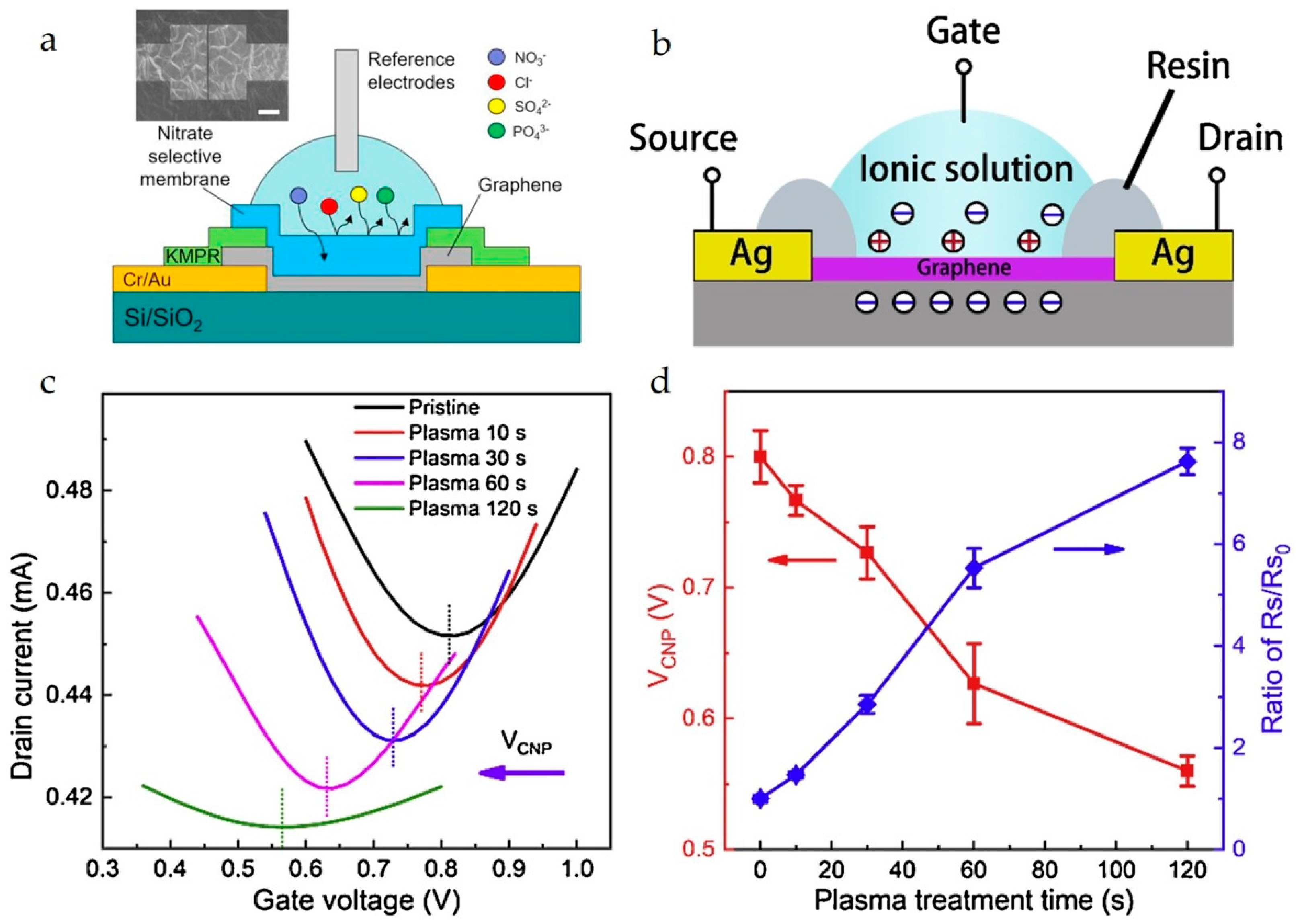
Graphene/nitrate selective polymer selective membraneNitrate ions in water0.1 mg/LDirac point shift of up to 0.25 VResponse time 10 sInterference from other ions present in water samples[21]
Graphene/valinomycin-based ion selective membraneK+ ionsN/A64 mV/decade between 10 µM and 20 mMResponse time 7.1 sSelectivity issues at concentration less than 10 µM; baseline interference[22]
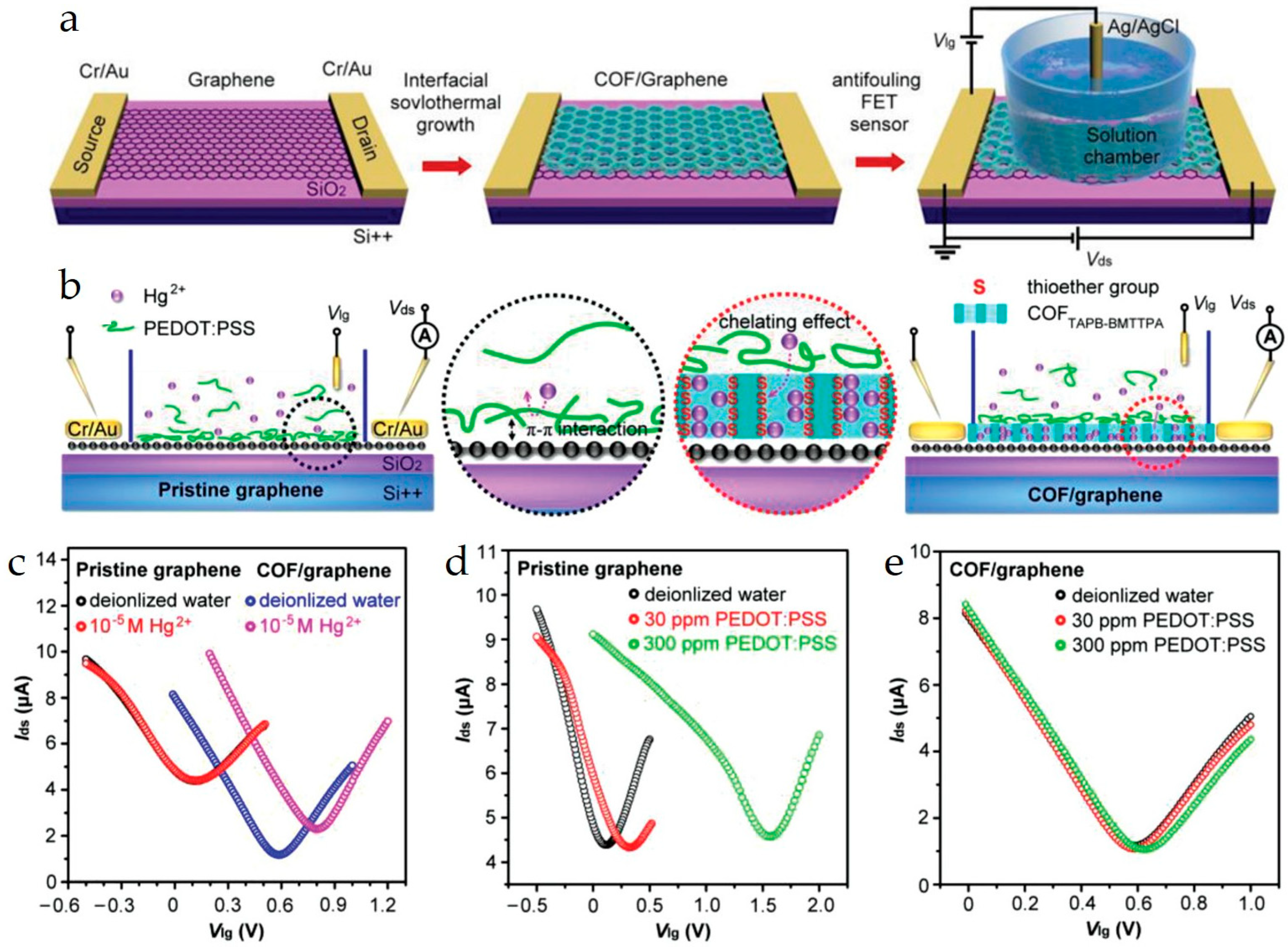
Graphene/covalent organic framework (COFTAPB-BMTTPA)Hg2+1 × 10⁻¹⁰ M10−10 M to 10−4 MResponse time 50 msNon-specific adsorption of interferents; the thickness of the COFTAPB-BMTTPA layer impacts sensitivity[23]
GrapheneK+ ions0.058 pMSensitivity coefficient was 0.0255N/AProlonged plasma treatment results in structural defects and poor conductance characteristics, limiting the device’s performance[28]
GrapheneK+, Na+, NH4+, NO3−, SO42−, HPO42−, Cl1 × 10−5 MK+: 45.7 mV per decade; Na+: 49.2 mV per decade; NH4+: 58.6 mV per decade; NO3−: −56.7 mV per decade; Cl: −43.0 mV per decade; SO42−: −22.6 mV per decade; HPO42−: −34.9 mV per decadeN/ATemperature and pH dependence; in multi-ion solutions, the system of equations occasionally fails to provide real solutions for anion concentrations[60]
GrapheneNH3130 ppbVoltage shift −0.057 per 10-fold increase in NH3 concentration from 9 to 2400 ppmResponse time was 33 s; recovery time varies from 180 to 1500 sNon-linear response; diffusion dependence of gas in ionic liquid; manual ionic liquid placement[69]
Graphene with ssDNA aptamerHg2+40 pM Response time less than 1 sEnvironmental interference; baseline variation[71]
Graphene with microfluidic channelpH in seawaterN/ASensitivity 23.98 mV/pH in 1 × PBS solution; 8.07 mV/pH in seawater solutionResponse time 1 minSensitivity reduction in seawater due to different ion types and concentrations compared to PBS[73]
Thiacalix[4]arene (TCA) immobilized grapheneCu2+1 µM200 mV for 300 µMResponse time 15 minFabrication complexity—TCA immobilization; sentivity saturation at analyte concentrations over 300 µM[74]
Reduced graphene oxide (rGO) functionalized with ion-imprinted polymer (IIP)Cd2+0.83 ppb0.14 ppb−1 in the range of 2–200 ppbResponse time 5 minFabrication complexity—RAFT polymerization process for IIP functionalization; pH dependence[75]
Graphene; DNA-functionalized gate electrodeAs(III)5 nM0.24 mV/nMN/AFabrication complexity—DNA probe synthesis, thiol modification, electrode functionalization, and blocking with BSA[76]
Nafion-coated graphenepH 115.2 mV/pH 8.05: 450%30 s/100 sInterference by K+ ion; pH range[78]
Carbon-dot-functionalized grapheneCo2+1 × 10⁻¹⁹ MN/AResponse time 165 sThe detection mechanism heavily relies on the carboxyl groups on the surface of carbon dots[79]
Carbon-dot-functionalized grapheneCu2+1 × 10⁻¹⁴ MN/AN/AInterference by other metal ions; the mechanism relies on the inner filter effect and amine groups on CQDs[80]
L-phenylalanine-functionalized grapheneNa+, Co2+, Al3+, Cu2+0.000017 nmol/L (femtomolar range) for Cu2+; Nanomolar range for Na+, Co2+, Al3+N/AReal-time responseThe device supports only three cleaning cycles before sensitivity begins to degrade[82]
GraphenepH2 × 10−430 V per unit change in pHRecovery time 10 sDevice and sensing characterization performed in ultra-high vacuum[86]
Graphene; Fe-N-C SAE-functionalized gate electrodeHg2+1 nM−30 mV/decade in the range from 30 nM to 3 μMResponse time less than 2 sDetection not possible in highly polluted environments with concentrations over 3 μM[87]
Zinc oxide (ZnO) nanoglobules (NGs) with graphene oxide (GO) and reduced graphene oxide (rGO)Cr (III) ions (ZnO-NGs@GO); Cu (II) ions (ZnO-NGs@rGO)Cr (III): ~7.05 μM; Cu (II): ~14.9 μMCr (III): ~49.28 mA μM−1 cm−2; Cu (II): ~185.32 mA μM−1 cm−2N/AThe adsorption process may become poor and achieve saturation over time due to the limited quantity of negative adsorptive sites on the electrode surface[88]
Grapheneorganophosphorus (OPs) pesticide0.05 pMN/AResponse time 35 minThe oxidation potential of thiocholine (TCh) is high (≈0.8 V vs. Ag/AgCl), and it requires a high gate potential operation[89]
Table 3. Comparison of the characteristics of different gate configurations.
FeatureBack-Gate (BG-FET)Solution-Gate (SG-FET)Extended-Gate (EG-FET)Dual-Gate (DG-FET)
MaterialsGraphene, MoS2, BP, MXeneGraphene, MoS2, rGO, COFsEG structure with 2D/oxide filmsGraphene, MoS2, In2Se3
FunctionalizationMetal nanoparticles (Ag, Pt), MOFs, ssDNA, metal oxides (SnO2, MoOx)Ionophores, aptamers, IIPs, CQDs, COFs, enzymesSensing films on separate electrode: SnO2, Al2O3, hBNSurface trapping layers, charge modulation layers, chemical gate tuning
Fabrication complexity *Low–ModerateModerate–HighModerateHigh
LODGases and ions to ppt/aMIons to aM, gases ~ppbIons, pH, proteins to pptGases/biomolecules to ppb/ppt
Response Time1–100 s (some up to min)Fast (ms to s)Typically fastVaries; suitable for real-time
Sample environmentGases, liquidsLiquids, ionic liquids, pHLiquids (biological, serum)Liquids, gases
AnalytesGases (NO2, NH3), VOCs, ionsIons (K+, Hg2+), DNA, pHpH, biomarkers, viral proteinsDNA, pH, gases
AdvantagesSimple, CMOS-compatible, versatileHigh sensitivity, real-time, low voltageSensor isolation, reusable transducerSignal gain, dual control, better in high-salt
Primary limitationsDrift, selectivity, contact noiseDrift, Debye effect, needs reference electrodeLarger footprint, moderate sensitivityFabrication difficulty
* The fabrication of complexity of different gate FET sensors is evaluated based on the number of steps required to complete the fabrication process. BG-FET sensor fabrication involves channel deposition/transfer, lithography patterning and electrode deposition (direct electrode deposition using a shadow mask in some cases). This is the basic step for all gate configurations and is considered as step one. SG-FETs require step one and an additional sample chamber building step. EG-FETs require step one on two substrates with an optional sample chamber building step. DG-FETs require carrying out step one two times with an optional sample chamber building step.
Disclaimer/Publisher’s Note: The statements, opinions and data contained in all publications are solely those of the individual author(s) and contributor(s) and not of MDPI and/or the editor(s). MDPI and/or the editor(s) disclaim responsibility for any injury to people or property resulting from any ideas, methods, instructions or products referred to in the content.

