Abstract
Considering the improvements to modern communications and its requirements, antennas need to operate optimally at certain frequencies and have smaller dimensions. This study considered the optimization of two single antennas functioning at 2.4 GHz through geometry modification while preserving or even improving their bandwidth, while also considering their gain. At first, the research was conducted using numerical modeling and, based on the conclusions drawn following this analysis, the next step was the experimental analysis of the structures. Due to their different geometrical appearances, the optimized antennas were compared, and then an optimum two-antenna MIMO structure was determined for both structures using different methods to decrease the mutual coupling. The optimum structure was obtained for both antennas. The new antennas functioned at 2.4 GHz but had different dimensions, thus a study into the decoupling methods was needed to see if the same methods were best for both cases. It was determined that shifting the two antennas in the MIMO was the better method when leaving a distance of λ/2 cannot be considered due to an increase in the dimensions of the structures, followed by a 90° shifting of the antennas. Also, the modification of the gain representation was observed through implementing the different decoupling methods to determine their influence on the beamforming.
1. Introduction
Planar antennas are an important part of technology today due to their small dimensions, easy manufacturing process, and versatility. They are used in a lot of applications, like satellites, radar, and mobile communication. The antennas must be designed such that they meet the needs of the user and are optimized to have the specific parameters like gain and bandwidth that are needed.
Once an antenna has been designed for a specific bandwidth, there is another challenge that needs to be faced, namely the influence of other antennas placed near it. There are a lot of cases where the same device has more than one antenna and, sometimes, they affect one another.
Traditionally, wireless communications used two antennas, one emitter and one receiver, but the transfer speed was limited. MIMO antennas use more than one antenna, sending more than one data flux simultaneously, which increases the data transfer speed. These types of antenna also use beamforming to increase the directivity of the signal. Their major advantages are efficiency, connectivity and mobility, flexibility and security, a higher data rate, the speed of data transmission, power saving, reliability, and the possibility of beamforming [1,2]
MIMO antennas have evolved in the past several years from two or four elements to massive MIMOs where there are more than eight antennas [1,2,3,4].
Through the use of different isolation methods to reduce mutual coupling, MIMO antennas can use the same frequency to send more fluxes simultaneously. There are a lot of methods to improve MIMO functionality, among them being neutralization lines [5,6], modifying the position of the antennas in relation to one another with certain angles, more often 90° and 180° [7,8,9], parasitic elements [10,11,12], defected ground structures [13,14,15], and decoupling structures [16,17,18,19]. There is also the use of metamaterials and reactive impedance surfaces to improve MIMOs, all while maintaining the smallest dimensions possible.
The main aim of this paper was to determine the optimized structure of two different planar antennas operating at 2.4 GHz with different dimensions and to include them in MIMO structures, while also determining which of the mutual coupling-reducing techniques worked better for them. The methods used were inserting a parasitic element between the antennas, increasing the distance between the antennas, creating a defected ground plane, and inserting a slot between the antennas. Also, the antennas were placed at a certain angle from one another, all while observing the S parameters of the structure to see the effects. The ECC (envelope correlation coefficient) and the DG (diversity gain) were determined for the studied structures because they reflect the diversity performance of the MIMO antennas.
Section 2 introduces the two initial antenna designs, both constructed on an FR4 dielectric substrate. The first was a planar Yagi–Uda antenna with dimensions of 56 × 65 mm, while the second was a planar dipole antenna, referred to as the “key antenna” due to its slotted design, measuring 32 × 20 mm. Section 3 details the optimization process, where the antenna dimensions were reduced while maintaining operation at 2.4 GHz. Section 4 explores the integration of these antennas into MIMO structures, evaluating their functionality and dimensions under different isolation techniques. Section 5 presents a discussion of the results, followed by the conclusions in Section 6.
2. Materials and Methods
To design MIMO antennas, the initial step involves developing an optimized structure for a single antenna operating at the desired frequency. This study examines two distinct antenna configurations designed for operation at 2.4 GHz, focusing on their optimization by reducing their dimensions. Cost efficiency was also considered in the material selection process, leading to the choice of FR4 as the dielectric substrate. The first antenna structure was previously investigated by our research group [19], while the second was obtained from the specialized literature [20].
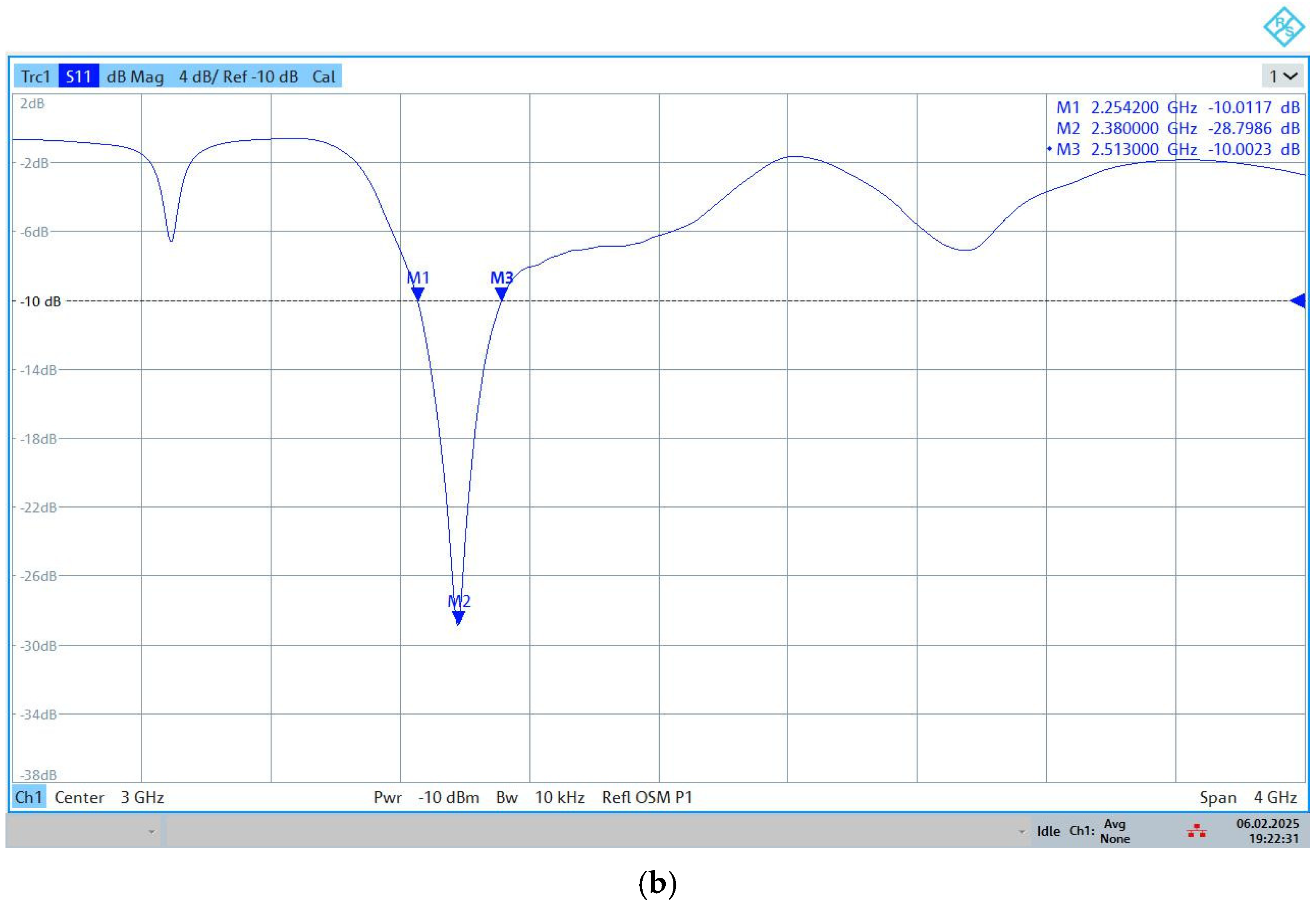
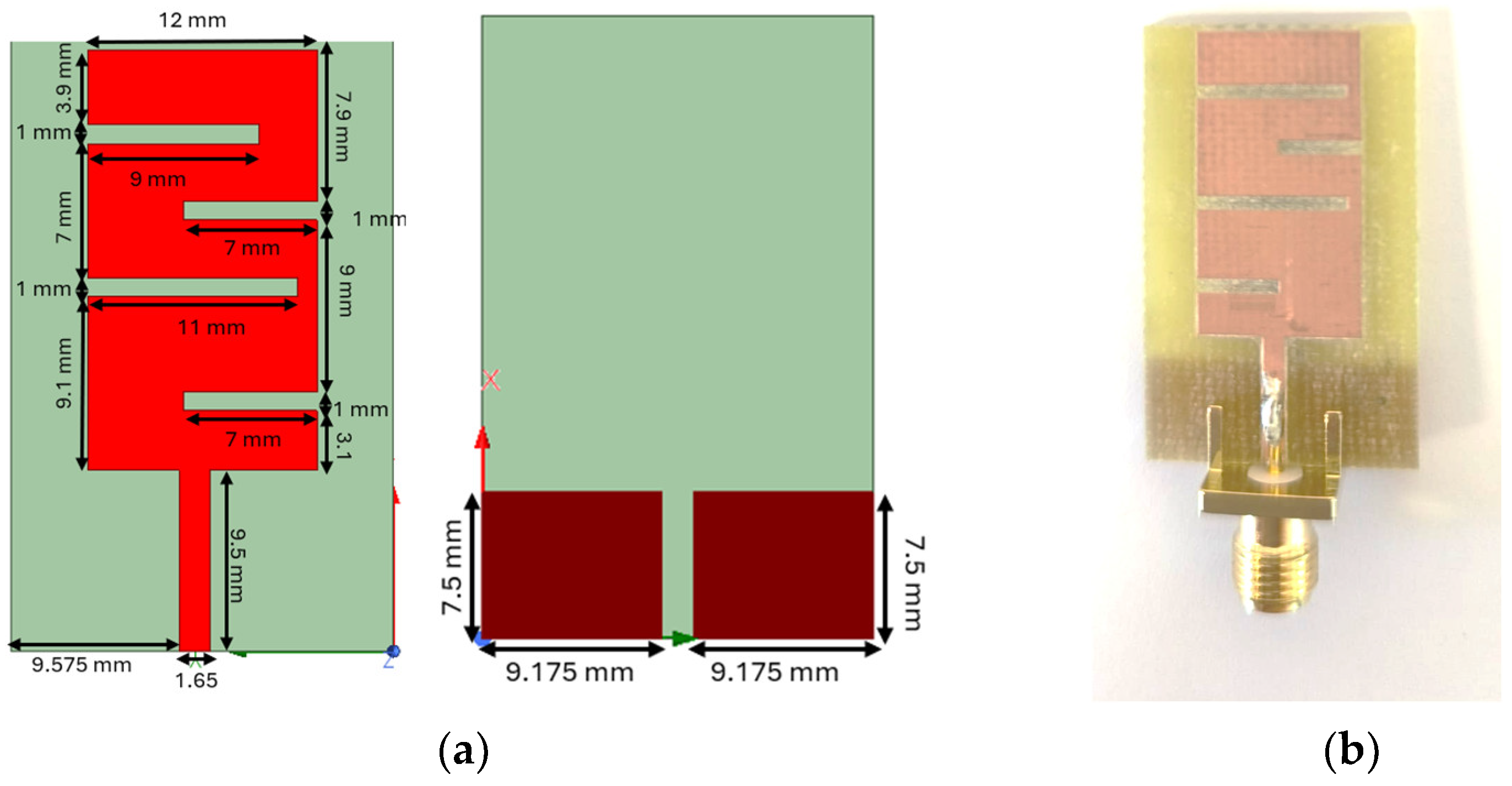
The first structure was a planar Yagi–Uda antenna, as described in [19], with dimensions of 56 × 65 mm, fabricated on an FR4 substrate with a thickness of 1.51 mm. The dimensions of its directors, radiator, and driven element are illustrated in Figure 1. The initial antenna operated within the frequency range of 2.254 GHz to 2.513 GHz, corresponding to an 11% bandwidth, calculated using Equation (2), where fc represents the central frequency, while f1 and f2 denote the lower and upper frequency limits, respectively. The numerical simulations performed using the software program for high-frequency numerical analysis Ansys HFSS 2023 R2 (High Frequency Structure Simulator) indicated that the antenna achieved a peak gain of 3.8823 and a radiation efficiency of 902.93.
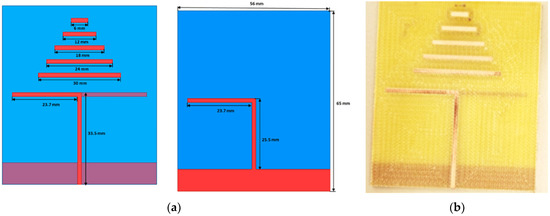
Figure 1.
The initial structure of the first antenna, considered to be optimized: (a) the dimensions of the antenna; (b) the practically constructed antenna.
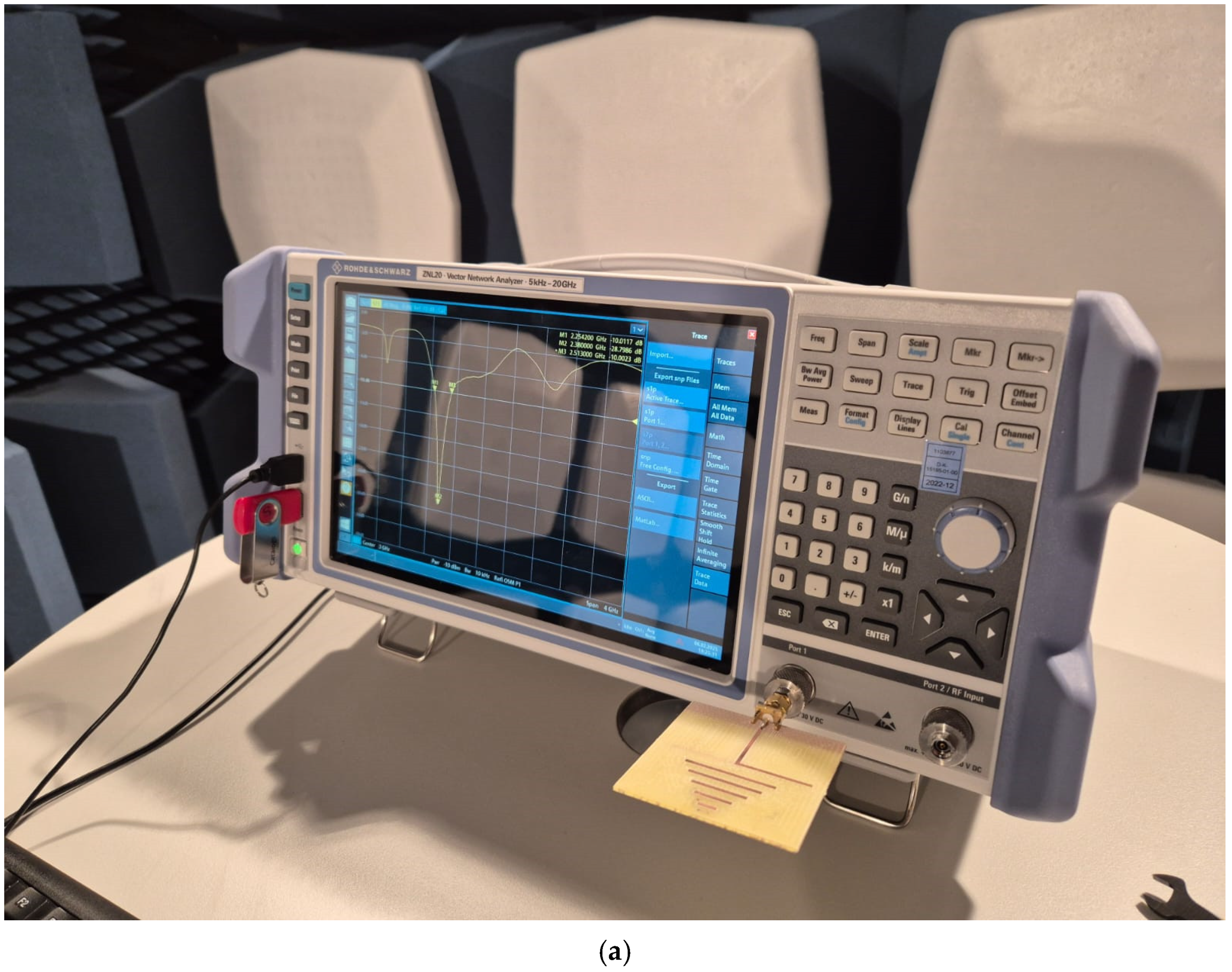
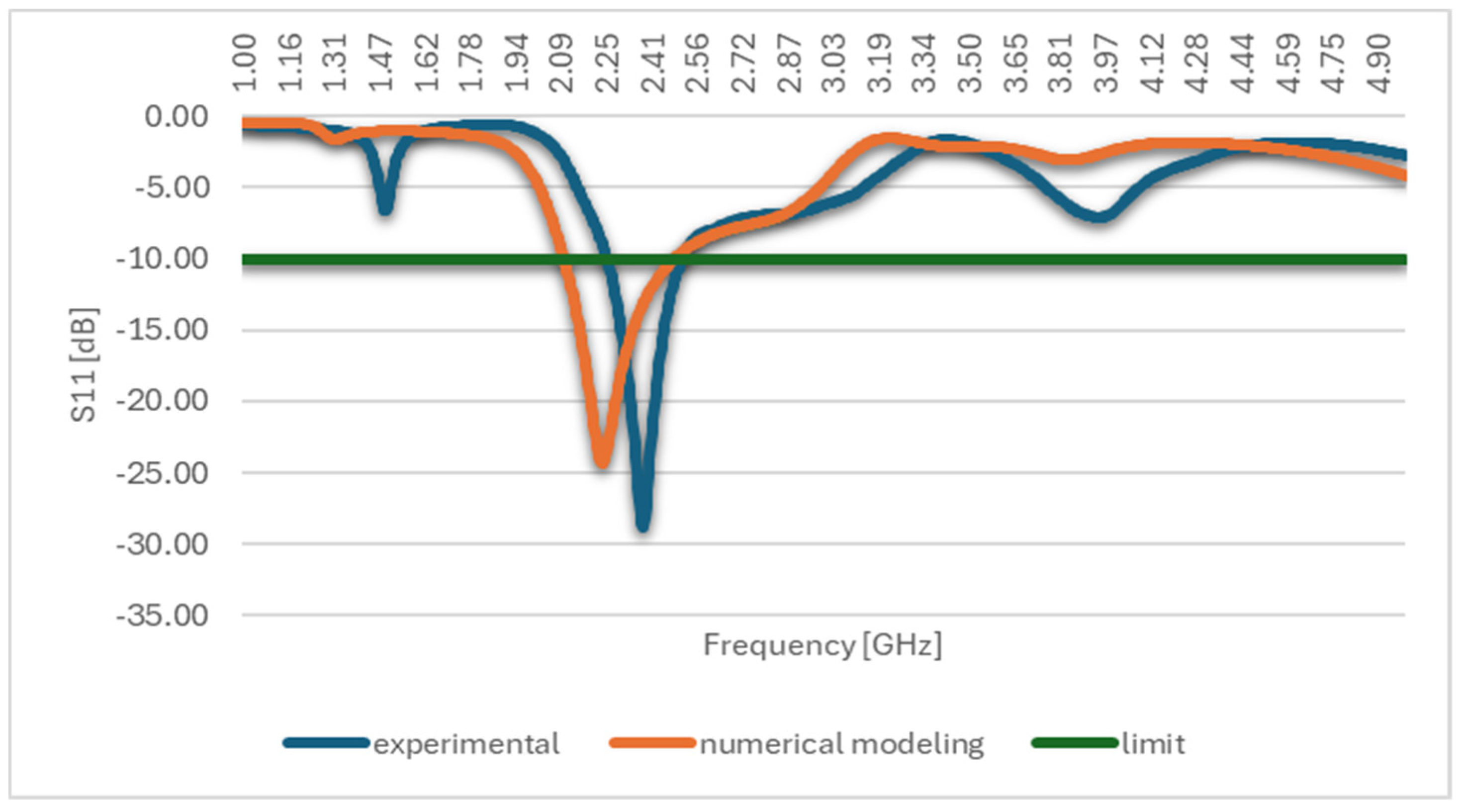
The initial antenna was fabricated on an FR4 dielectric substrate using the LPKF plotter, as illustrated in Figure 1b. Its S parameters were measured using a Vector Network Analyzer (VNA) (Figure 2) within a semi-anechoic chamber to validate the numerical simulations. As shown in Figure 3, a strong agreement was observed between the numerically and experimentally obtained results.

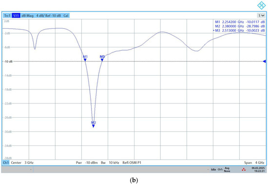
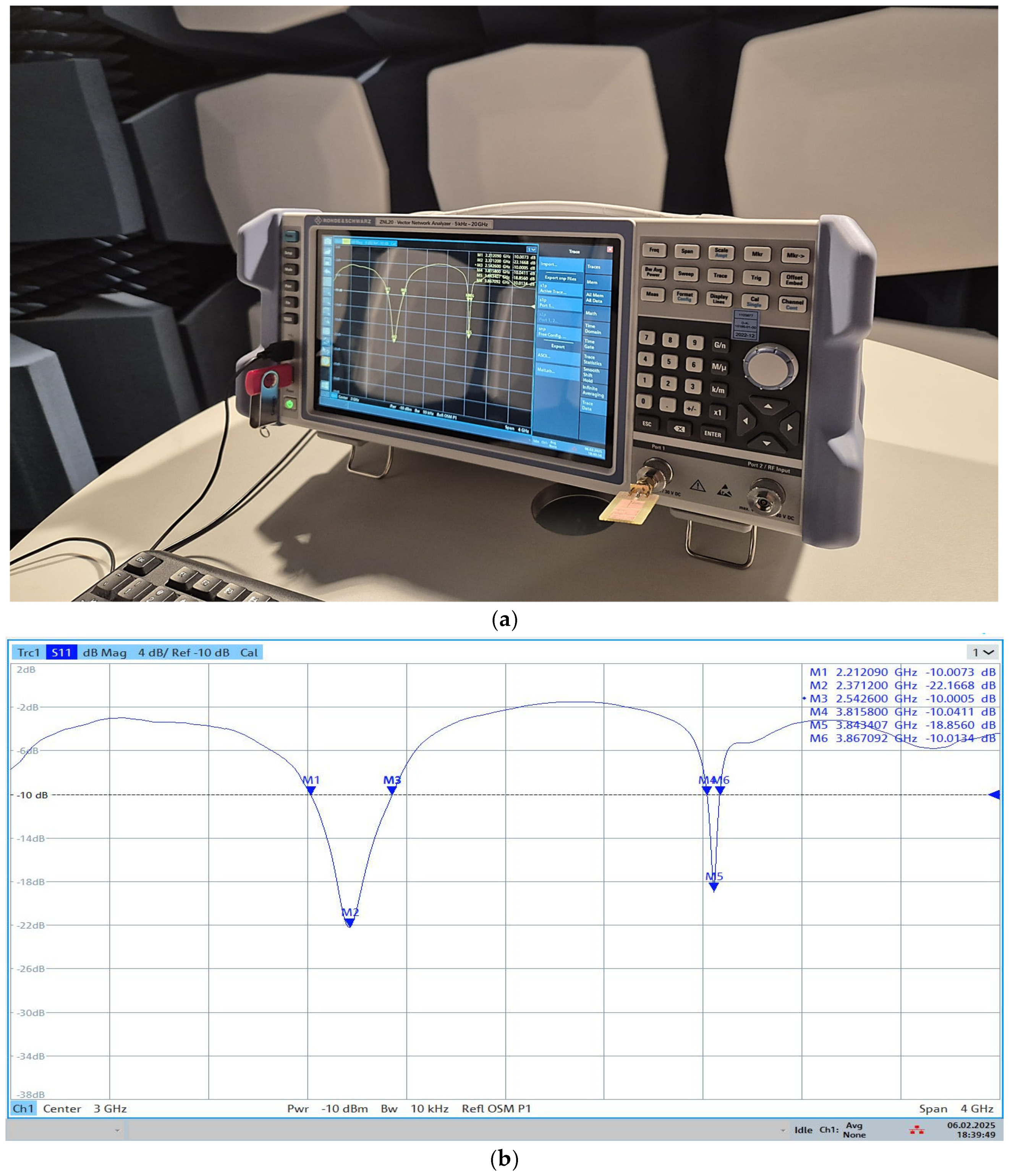
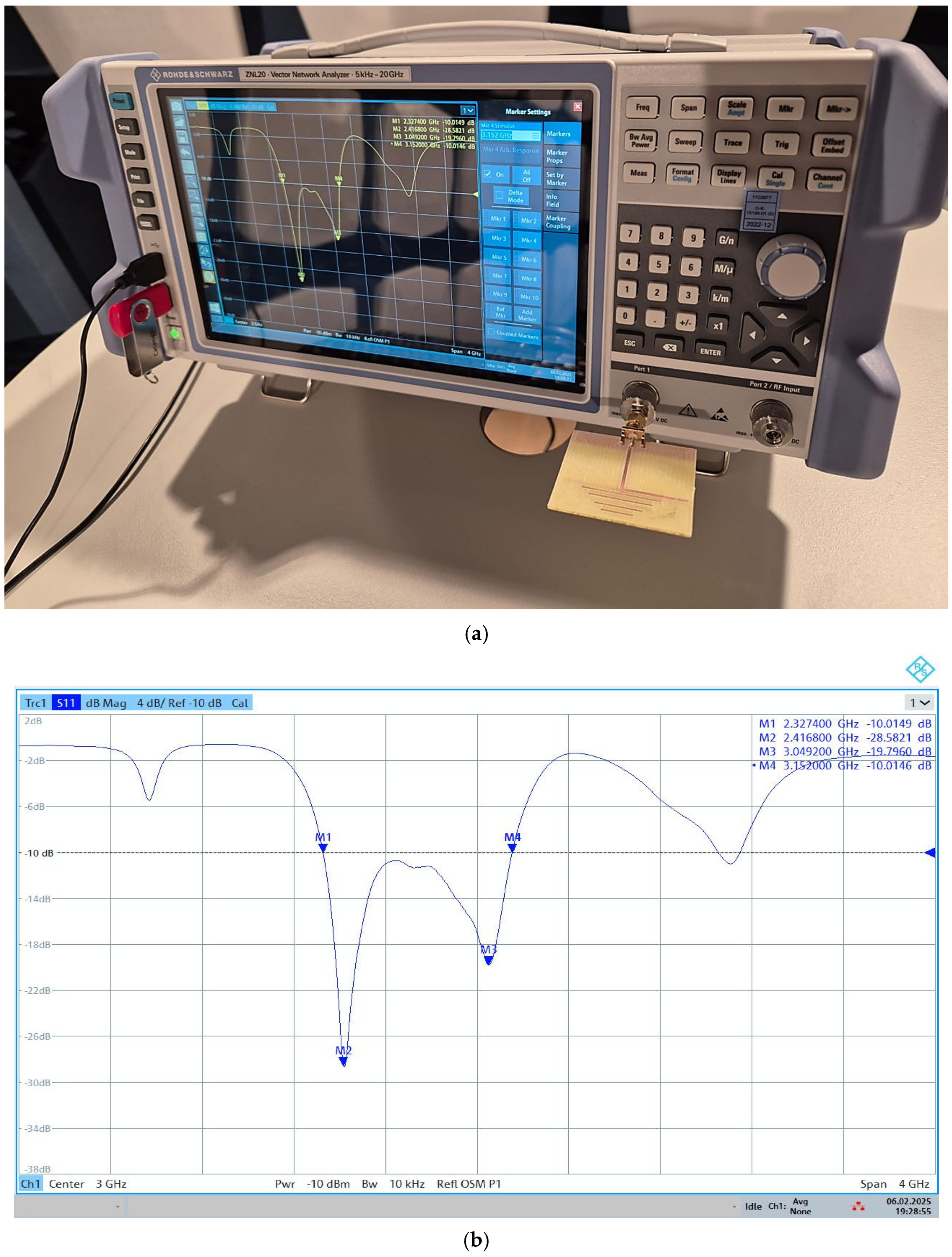
Figure 2.
Measurement of the S parameters for the initial structure: (a) the measurement stand; (b) the results given by the VNA.
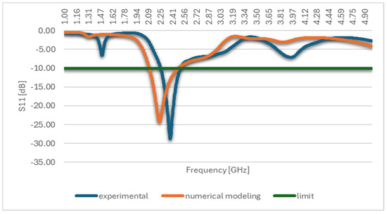
Figure 3.
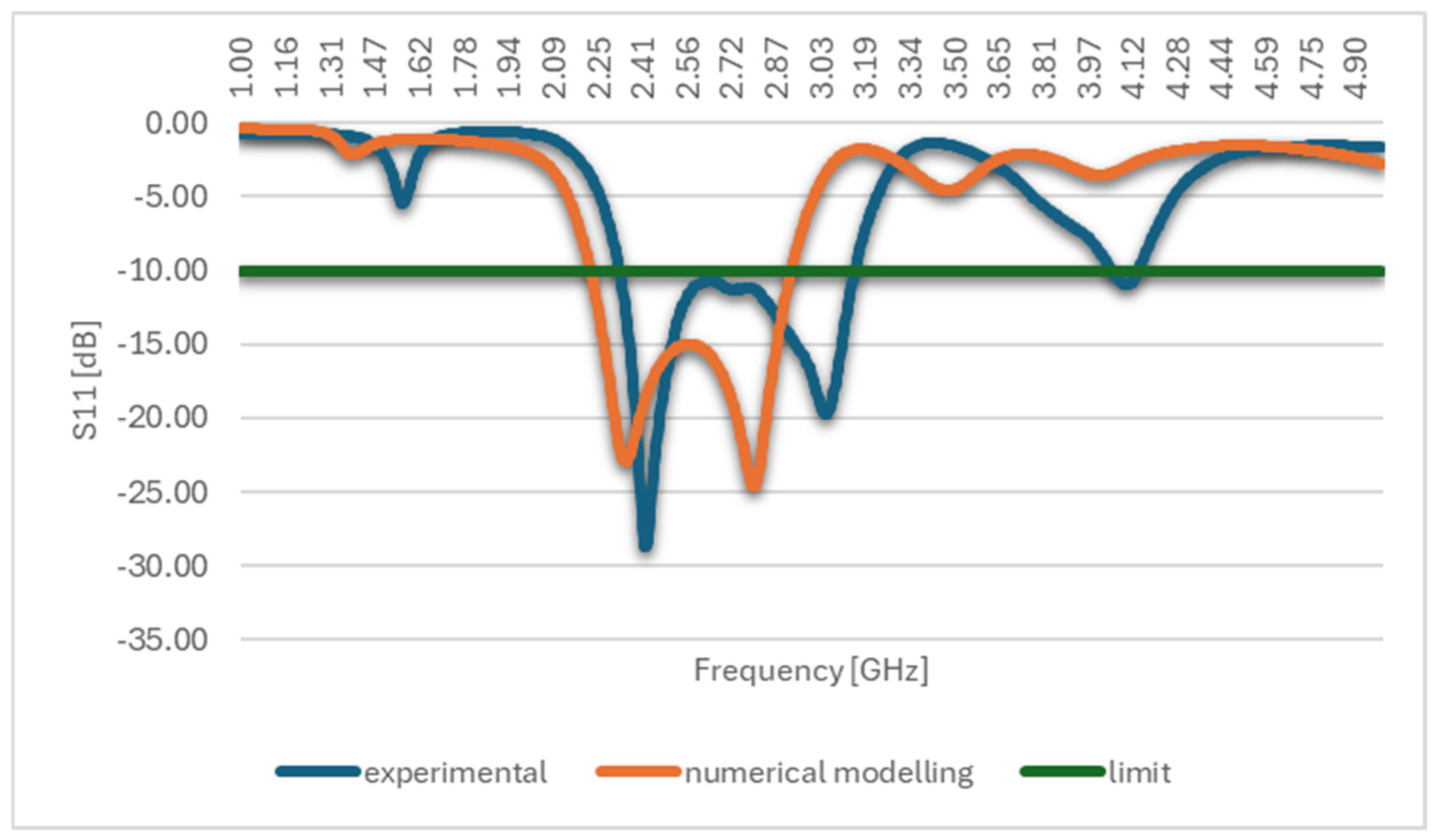
Comparison between the numerically modeled and the experimental S parameter values for the initial structure.
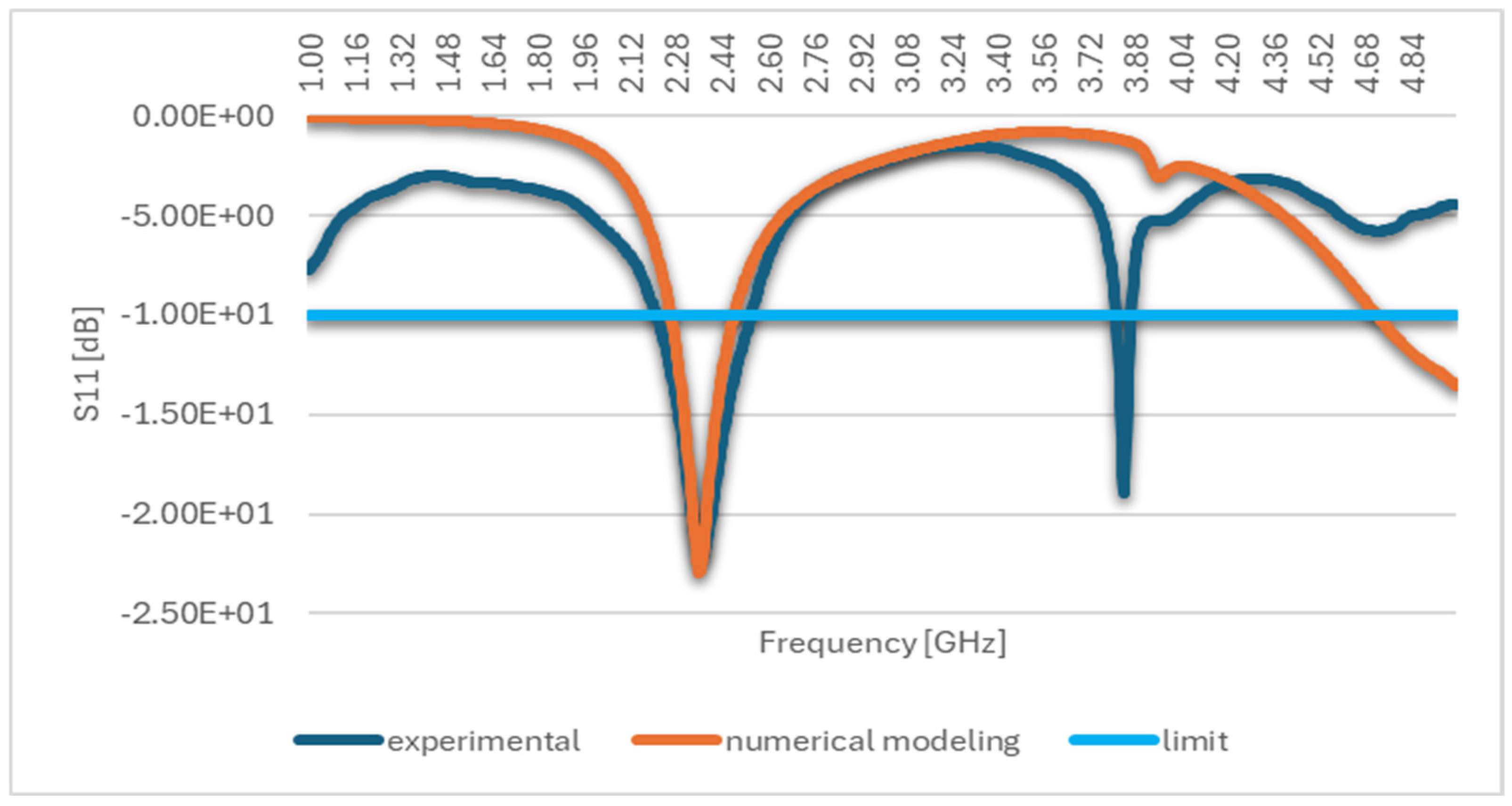
The second optimized antenna, initially presented in [20], was significantly smaller, with dimensions of only 20 × 32 mm, and we aimed to reduce its size further. The first step was to fabricate this antenna on an FR4 dielectric substrate with a thickness of 1.51 mm, whereas the dielectric thickness reported in the literature was 1 mm. The dimensions of this antenna, as well as the antenna fabricated with the LPKF plotter, are shown in Figure 4. The newly fabricated antenna operated within the frequency range of 2.212 GHz to 2.542 GHz, resulting in a 14% bandwidth around the 2.4 GHz central frequency (Figure 5). The results obtained through numerical modeling and experimentally can be observed as a comparison in Figure 6. It achieved a maximum gain of 1.63 and a radiation efficiency of 0.977.

Figure 4.
The initial structure of the second antenna, considered to be optimized: (a) dimensions of the antenna; (b) the practical constructed antenna.

Figure 5.
Measurement of the S parameters for the second initial structure: (a) the measurement stand; (b) the results from the VNA.
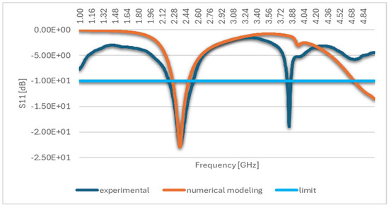
Figure 6.
Comparison between the numerically modeled and the experimental S parameter values for the second initial structure.
The gain patterns of the two antennas exhibited significant differences, which would influence their performance when integrated into MIMO structures. The polar plot depicting the gain distribution for both antennas is shown in Figure 7.
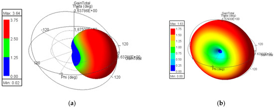
Figure 7.
Representation of the gain in polar plot for the two initial structures: (a) Yagi–Uda antenna; (b) key antenna.
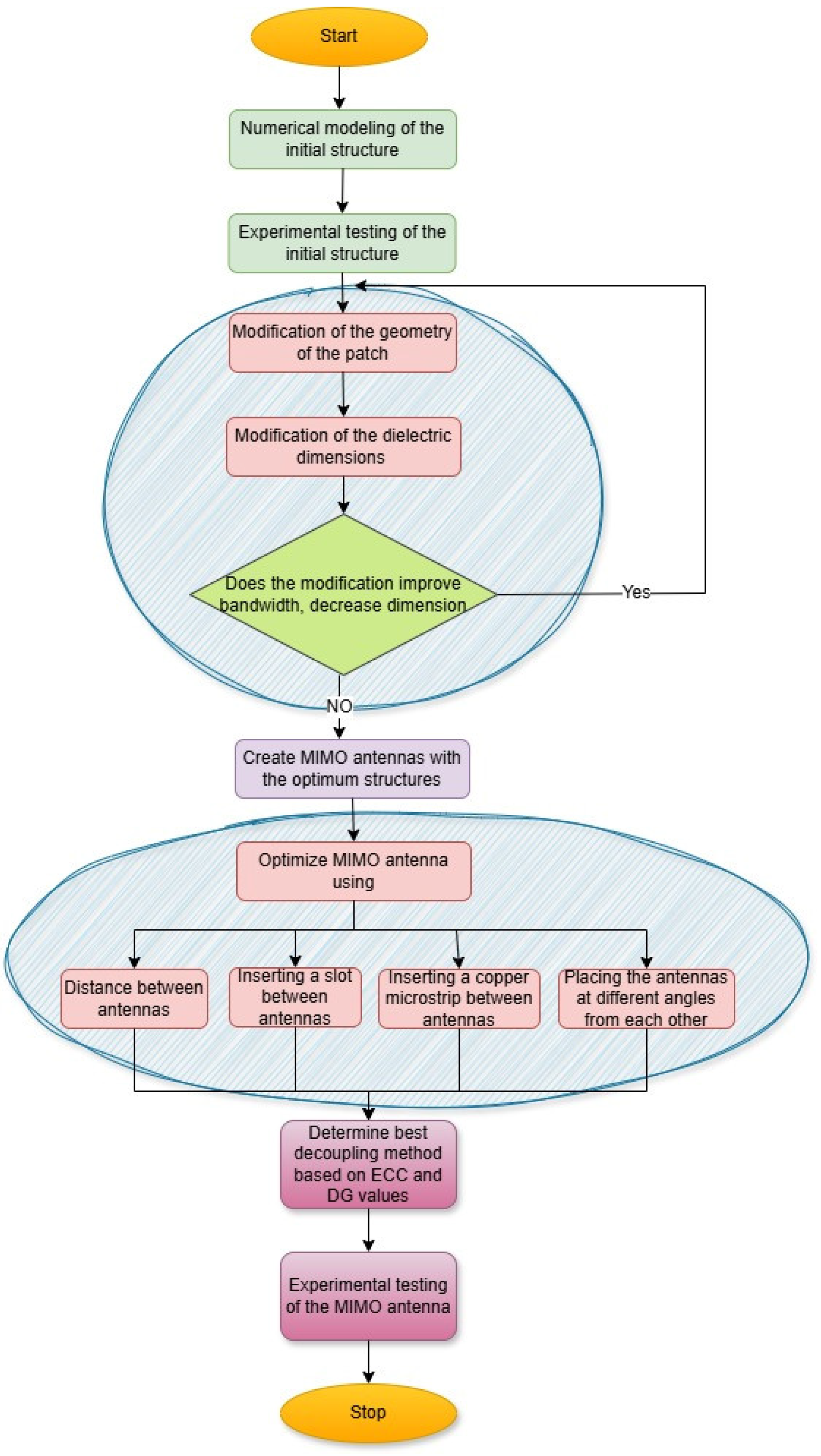
The main focus of this paper was to optimize these two structures and to use them to create reliable MIMO structures that are as small as possible. For this purpose to be achieved, the steps presented in Figure 8 had to be followed. Because of the different geometries of the structures, the specific stages of the optimization process could not be generalized, but the purpose remained the same: namely, to decrease the dimensions of the antennas while ensuring they functioned properly for the considered frequency. The optimization process considered for both antennas had the same steps: modifying the geometry of the patch, which was specific for each patch, and, if possible, modifying the dimensions of the dielectric to improve its parameters of interest.

Figure 8.
The different stages that were used to create a reliable MIMO structure.
After the optimum structure had been determined, the MIMO antenna was created. This new structure also had to be optimized by finding the best and most suitable decoupling method from the ones stated in Figure 8, all while considering the best results when calculating specific parameters like ECC and DG. The study concluded with the experimental testing of the MIMO antennas.
3. Results
Although both of the antenna structures discussed in the previous section were efficient, they were larger than desired, particularly the Yagi–Uda antenna. As a result, reducing their dimensions was a key objective. The optimization process for each of the structures, considering their specific characteristics, is outlined in this section. Defining an optimal antenna is challenging, as some designs prioritize higher gain while others focus on broader bandwidth. In this case, the goal was to minimize the antenna’s area while ensuring it operated effectively at 2.4 GHz, maintaining good gain and radiation efficiency.
3.1. Optimizing the First Antenna Structure
For the first structure, a reduction in size was required while preserving the resonant frequency. The logical approach followed in the research process, along with all of the steps undertaken, is illustrated in Figure 9.

Figure 9.
The logical scheme used for optimizing the Yagi–Uda antenna.
The thickness of the directors (g) varied between 0.1 mm and 1.5 mm, with an increment step of 0.2 mm, using the Optimetrics module of HFSS. The design with the directors measuring 0.9 mm was determined to be optimal. This antenna operated within the frequency range of 2.098 GHz to 2.435 GHz, resulting in a percentage bandwidth of approximately 14%. The S parameters for the structures considered are shown in Figure 10. This antenna was selected due to its prominent resonant frequency, which reached a value of 35.4 dB.
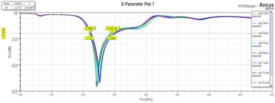
Figure 10.
The S parameters for the variation of director thickness for the Yagi–Uda antenna.
To further reduce the dimensions of the structure, the next step involved adjusting the distance between the directors (d) to ensure the antenna operated at 2.4 GHz while occupying a smaller surface area. The distance between the directors was parametrized and varied between 1.5 mm and 5 mm, with a step of 0.5 mm. This distance was measured from the bottom-left corner of one director to the same corner of the next director. Additionally, the distance between the driven element and the first director was kept constant at 1.5 mm. The bandwidth of the antennas considered remained similar, ranging between 31% and 33%, which represented a 15% increase from the previous step (Figure 11).
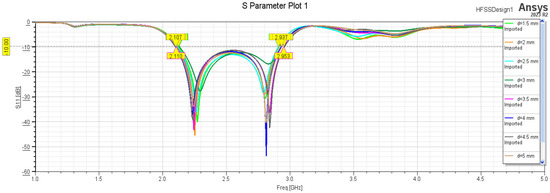
Figure 11.
The S parameters for the variation of the distance between the directors for the Yagi–Uda antenna.
To evaluate the gain, the maximum value was obtained for the antenna with a 3 mm distance between the directors, reaching a peak gain of 3.33. As expected, the gain was slightly decreased compared to the initial structure, but this allowed for a reduction in the antenna’s overall dimensions.
The third step involved adjusting the position of the ground while reducing the dimensions of the dielectric and the driven element. This was achieved by parameterizing the movement of the bottom-left corners of the dielectric, the driven element, and the ground while maintaining their dimensions. This parameter varied between 0 mm and 3 mm, with a step of 0.5 mm. As a result, the dimension was reduced by 1 mm, with the characteristic parameters remaining consistent with those of the optimal design based on the distance between the directors.
Additionally, modifications were made to the lengths of the directors, the driven element, and the reflector; however, these changes negatively impacted the bandwidth and the resonant frequency. Ultimately, by adjusting both the distance between the directors and the position of the ground, the dielectric was reduced to dimensions of 49 × 47 mm. As an example, Figure 12 represents the parameters g and d that were varied to determine the S parameters shown in Figure 10 and Figure 11, along with a few intermediate structures and the final optimized design.
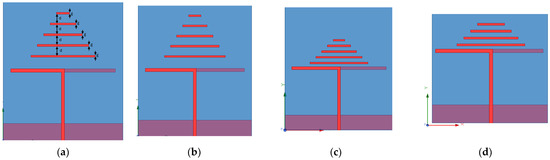
Figure 12.
Representation of the parameter variations used to determine the optimum values: (a) representation of the g and d parameters varied; (b) thinner directors; (c) smaller distance between the directors; (d) optimum antenna with smaller dielectric.
The optimized structure was fabricated and tested to verify whether the numerical modeling results aligned with the experimental measurements. Figure 13 presents the VNA measurements, while Figure 14 clearly shows the differences between the initial and the optimized antennas. A comparison of the S parameters for the numerically modeled and measured optimized structure is provided in Figure 15, demonstrating a close match.
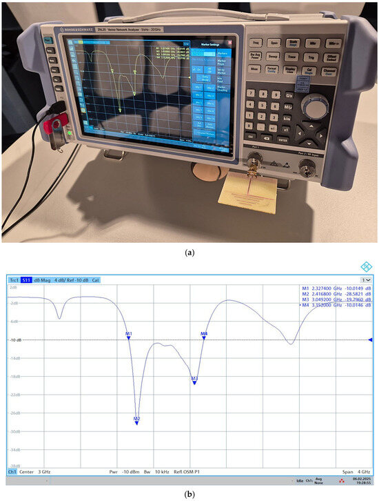
Figure 13.
Measurement of the S parameters for the optimum structure of the Yagi–Uda antenna: (a) the measurement stand; (b) the results from the VNA.
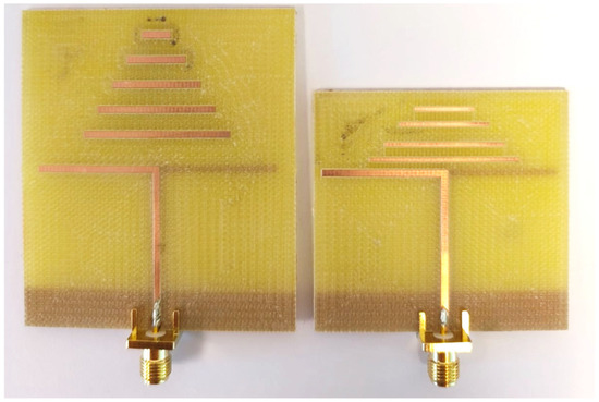
Figure 14.
Comparison between the initial and the optimized structure.

Figure 15.
Comparison between the numerically modeled and the experimental S parameter values for the optimized initial structure of the Yagi–Uda antenna.
Based on the measurement data, it was concluded that the optimized antenna exhibited a bandwidth of 26.9%. Furthermore, the gain pattern remained consistent with that of the initial structure.
For each structure considered, there were some minor discrepancies between the results obtained from the numerical modeling of the structure and the experimental results. Since the VNA was properly calibrated and the resulting S parameter graphs were given for the same number of measuring points, this was not the cause of the differences. Also, the measurements were conducted in a semi-anechoic chamber, which is considered a safe environment with no interference from the exterior. The factors that could have affected the results were the connection cables between the VNA and the antenna (because we know that for measurements at higher frequencies, special cables must be used, and they must not be bent) and the minor geometric variations that can occur when manufacturing the antenna or the solder joints of the SMA on the antenna.
3.2. Optimization Process for the Second Antenna Structure
The second antenna structure, as previously mentioned, was initially constructed on a thinner FR4 substrate, which resulted in different characteristics when considering the S parameters. In an effort to modify the structure so that it resonated at 2.4 GHz, we adjusted the slots, as they were found to significantly influence the resonant frequency. After evaluating several geometries, the initial structure was chosen, as shown in Figure 4. Similar to the previous case, a plan detailing the various steps taken to achieve the optimum design is presented in Figure 16.

Figure 16.
The logical scheme used for optimizing the key antenna.
The first step in the optimization process involved modifying the width of the antenna; however, it was determined that the initial width was the most suitable for achieving the desired resonant frequency.
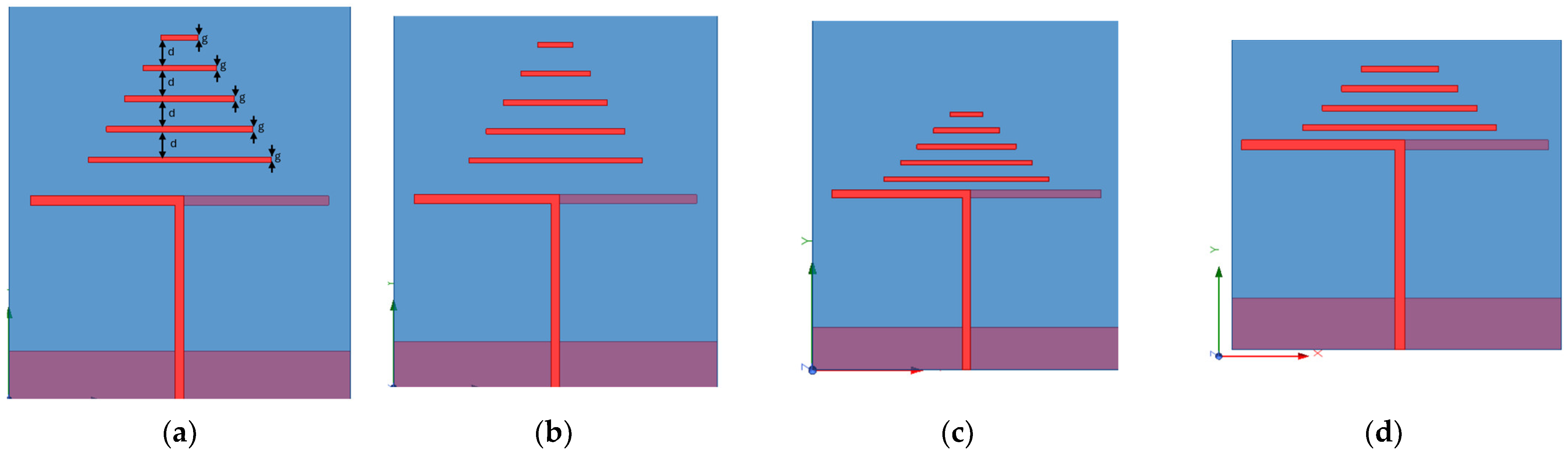
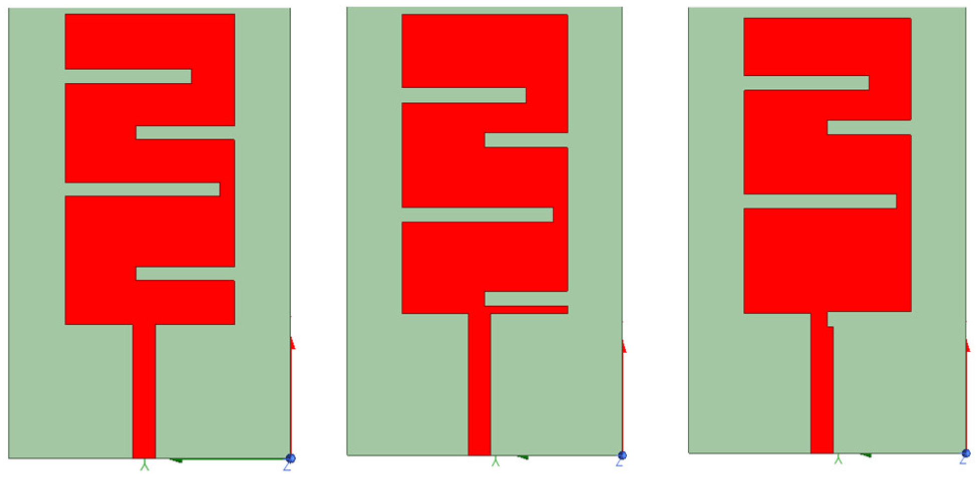
The next step focused on determining the optimal positioning of the slots. The goal was to position them in a way that would reduce the overall dimensions of the patch. A total of 875 possibilities were analyzed. Several configurations were considered, and some of them are presented in Figure 17. However, the variations in bandwidth at 2.4 GHz were found to be too small to warrant consideration. On the other hand, the length and placement of the slots were found to have a significant impact on the antenna’s performance at higher frequencies, enabling it to operate across multiple bandwidths.
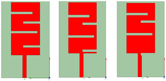
Figure 17.
Some of the possibilities considered for the slot positioning.
When the overall length of the patch was reduced, the results did not show any improvement. Therefore, the initial structure was considered the optimal design for the 2.4 GHz frequency. Additionally, the shape and size of the ground were found not to be parameters that could enhance the antenna’s performance.
4. Analysis of the MIMO Antennas Constructed from Two Antennas
When two antennas are placed next to each other, the signals emitted by them interfere with one another and are distorted. That is why there are a lot of methods to decouple the antennas while keeping the MIMO structure small. For this study, the initial and optimized antennas were inserted into the MIMO and some of the different methods were applied to maintain their optimal functions, all while keeping the structures as small as possible. The study considered the use of two antennas to construct the MIMO. For each of the structures considered, the effective correlation coefficient (ECC) and the diversity gain (DG) were determined [1].
DG arises from the spatial diversity of multiple antennas. This parameter influences the reliability of communication between antennas and the radiation coverage area and is calculated with Formula (3). The closer this parameter is to 1 the better in terms of the antennas not interfering with one another [2].
ECC refers to the independence of the antennas, taking into account the shape, polarization, and relative phase of the radiating elements, and is calculated with Formula (4). A value lower than 0.5 is considered optimal [2].
4.1. MIMO Antennas Constructed from the Yagi–Uda Planar Antenna
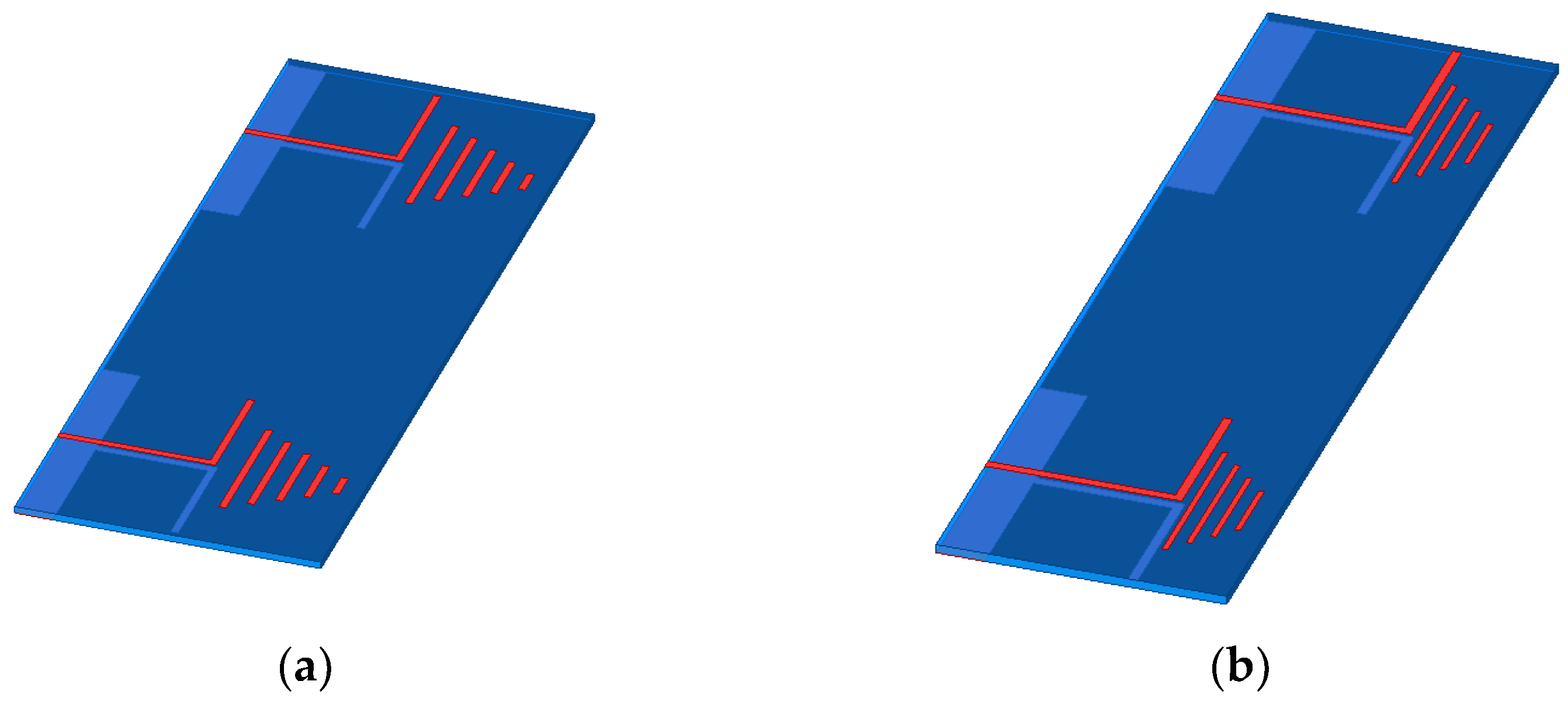
The initial structures for the two-antenna MIMO configuration are shown in Figure 18, which presents both the initial and the optimized designs. The antennas were placed adjacent to each other without any spacing. The impact of the optimization was clearly visible, with the first structure having dimensions of 112 × 65 mm, while the optimized version measures only 102 × 48 mm.
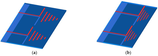
Figure 18.
The initial two-antenna MIMO for: (a) the initial structure; (b) the optimized structure.
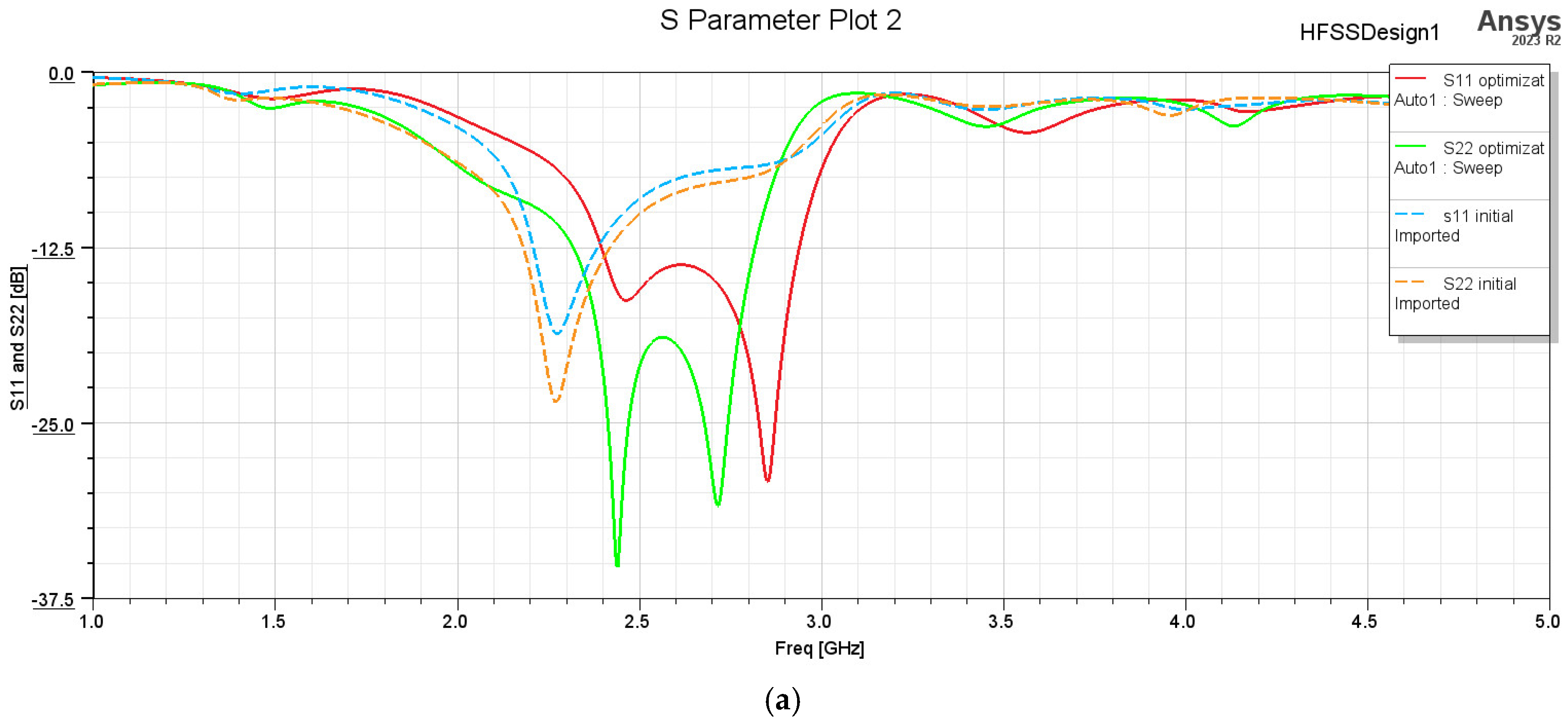
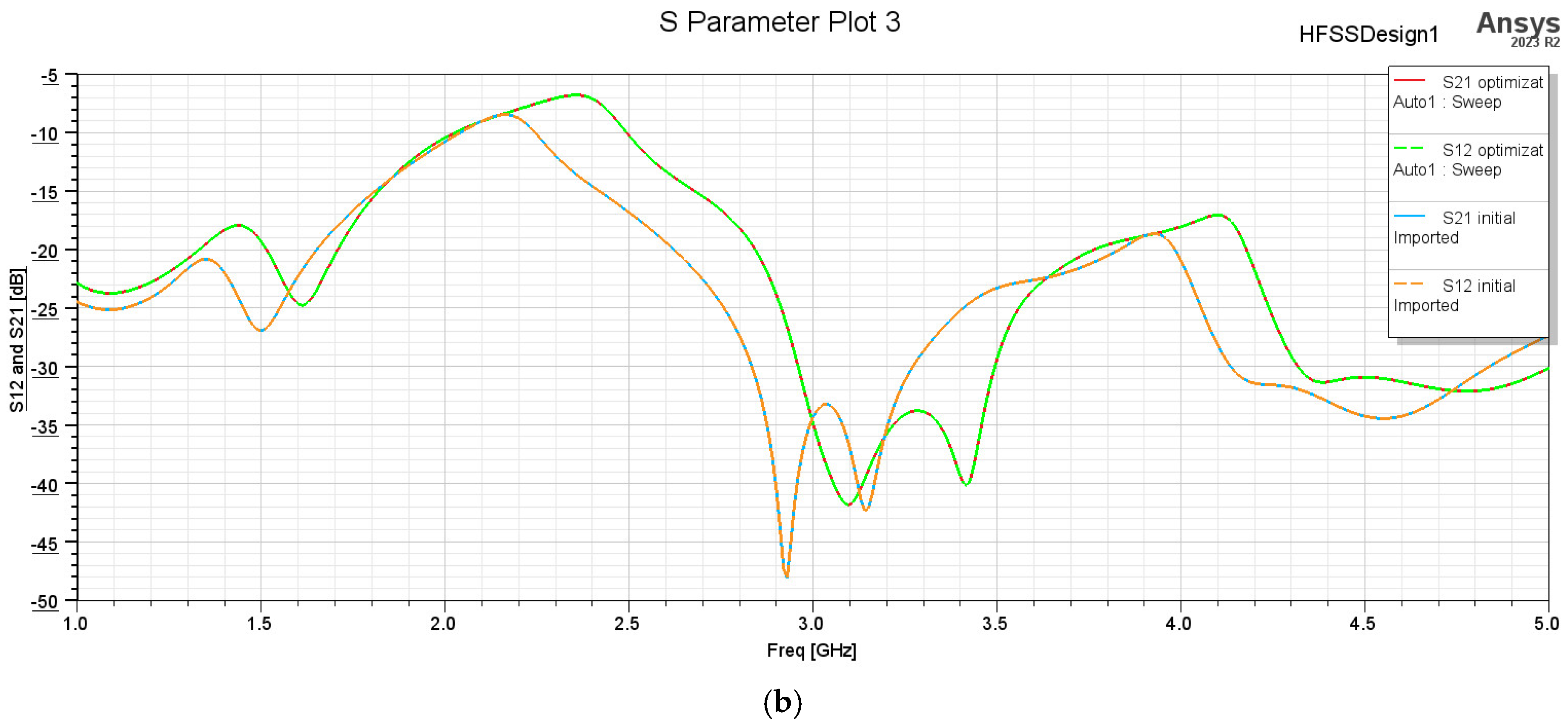
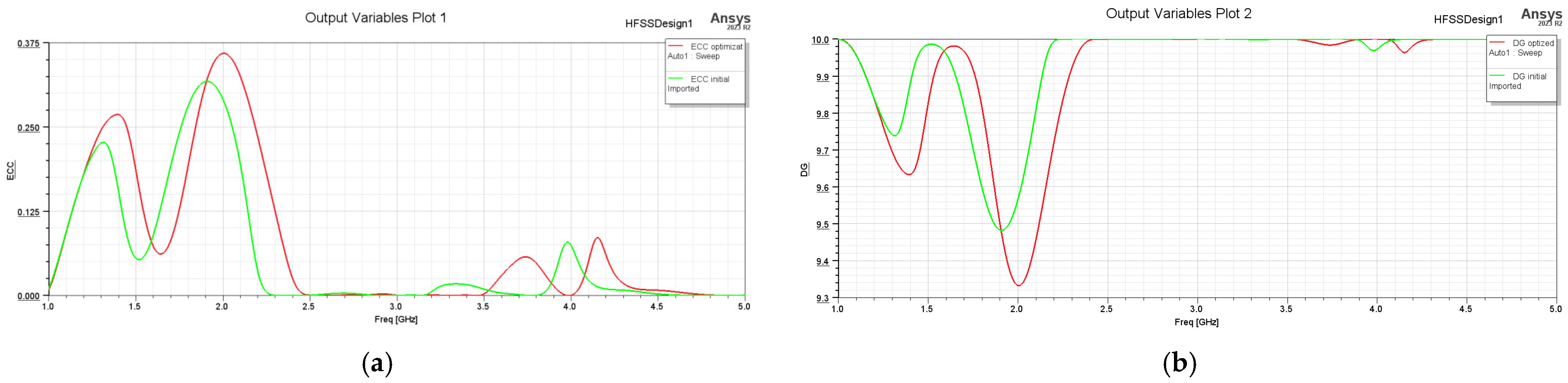
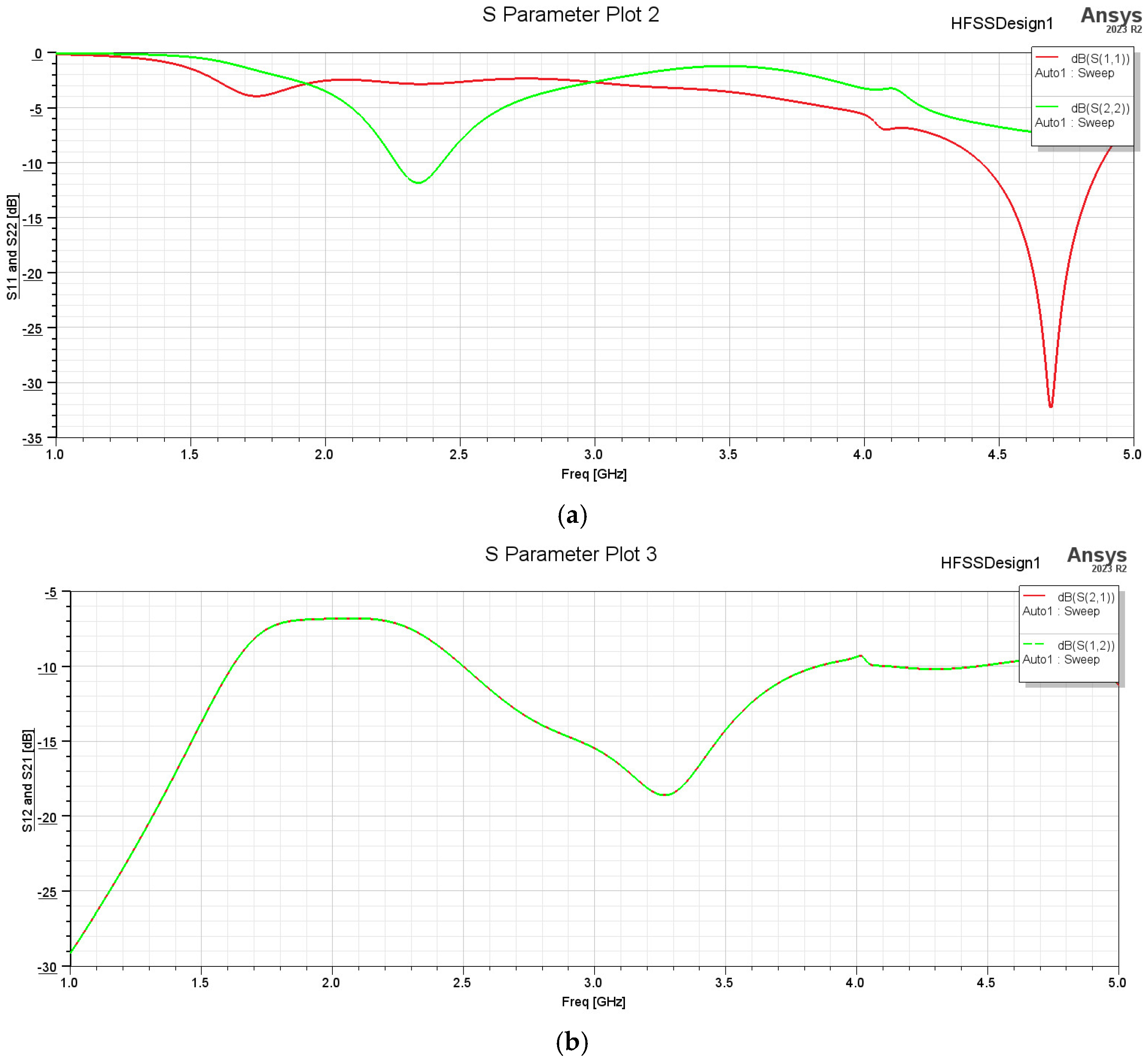
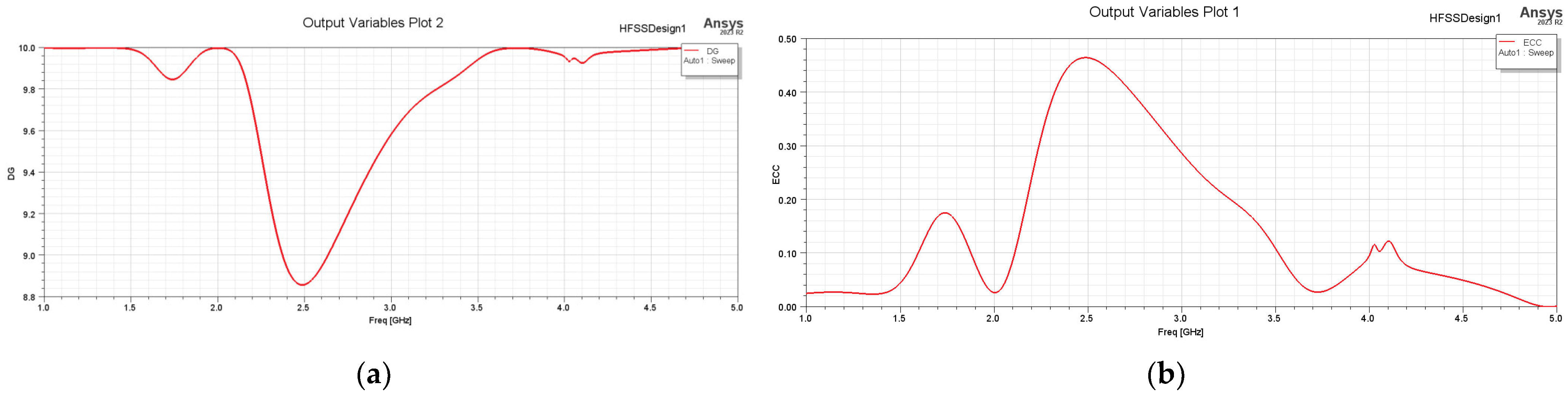
The S parameters for the antennas are presented in Figure 18, with S11 and S22 presented in Figure 19a, and S12 and S21 in Figure 19b. The envelope correlation coefficient (ECC) and the diversity gain (DG) for these antennas were calculated using HFSS over a frequency range of 1 to 5 GHz, as shown in Figure 20. Although the ECC was below 0.5, indicating good isolation (Figure 20), there were noticeable spikes near the frequency at which the antenna was intended to operate. Additionally, the DG was far from the ideal value of 10, at around 2.4 GHz. Furthermore, S11 and S22 did not align for the two antennas, emphasizing the necessity of employing the previously discussed methods to reduce mutual coupling between them.

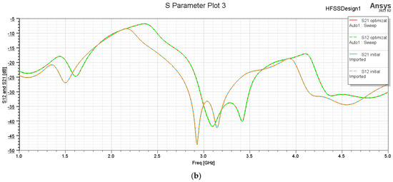
Figure 19.
The S parameters for the MIMO antennas considering the initial and optimum structureof the Yagi-Uda antenna: (a) S11 and S22; (b) S12 and S22.
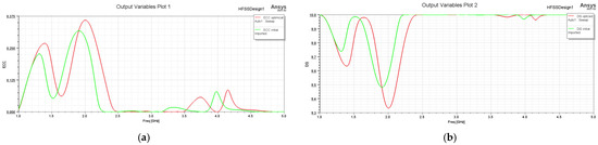
Figure 20.
The parameters used to characterize the MIMO antenna for the initial and optimized Yagi-Uda antenna: (a) ECC; (b) DG.
The initial technique employed involved increasing the distance between the antennas to λ/2, as this is widely regarded in the literature as an effective method for minimizing parasitic coupling between antenna elements [21,22,23,24,25]. However, a significant drawback of this approach is the increase in the overall antenna area. For a frequency of 2.4 GHz, the corresponding distance was calculated to be 62.5 mm, using the Formula (5), where λ represents the wavelength, c is the speed of light, and f is the operating frequency (2.4 GHz in this case). This resulted in a calculated separation of 62.5 mm [26].
The structures, as depicted in Figure 21, now had increased dimensions, with the initial structure measuring 174.5 × 65 mm and the optimized structure measuring 164.5 × 48 mm. Additionally, the grounding had been discontinued.

Figure 21.
MIMO antenna with λ/2 between the antennas: (a) initial structure; (b) optimized structure.
The second method involved inserting a metallic strip between the antennas as a parasitic element. Due to the presence of the directors, the strip could not be too thick; therefore, a 2 mm wide metallic strip was placed between the antennas (Figure 22). Two placement options were considered: one where the metallic strip was positioned on the top surface of the dielectric, and the other where it was placed on the bottom surface, extending as a continuation of the ground layer. The dimensions of the structures were maintained as those presented in Figure 18.
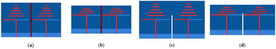
Figure 22.
MIMO antenna: (a) metallic strip initial structure; (b) metallic strip optimized structure; (c) slot initial structure; (d) slot optimized structure.
Also, a slot with a length of 35 mm, a width of 2 mm, and a thickness of 2 mm was created between the antennas. This design took into account the mechanical stability of the structures, ensuring they could withstand the potential risks while also considering the small distance between the directors. The resulting structures are shown in Figure 22c,d.
The fourth method was represented by rotating the antennas at specific angles. This approach was considered the most effective in terms of the ECC, the S parameters, and the DG, although it altered the shape of the antenna. When the initial antenna was rotated by 90°, its dimensions became 121 × 65 mm, while a 180° rotation resulted in dimensions of 130 × 56 mm. For the optimized antenna, the MIMO structure with a 90° rotation of the second antenna measured 51 × 99 mm, and with a 180° rotation, it measured 51 × 96 mm (Figure 23).
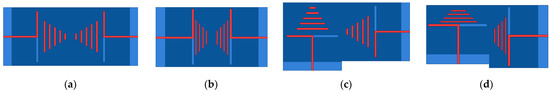
Figure 23.
MIMO antenna with antennas rotated at certain angles: (a) two initial structures at 180°; (b) two optimized structures at 180°; (c) two initial structures at 90°; (d) two optimized structures at 90°.
4.2. MIMO Antennas Constructed from the Key Planar Antenna
For the second antenna, the same decoupling methods were applied. Seven different structures were designed and analyzed, with comparisons made based on their S parameters, ECC, and DG, all while aiming to minimize their dimensions. The initial structure, where the antennas were placed directly next to each other, is shown in Figure 24. The corresponding S parameters for this configuration are presented in Figure 25, while the ECC and DG are shown in Figure 26. In this case, the antennas were significantly affected by parasitic coupling, leading to suboptimal MIMO performance, as indicated by the ECC values being close to 0.5. The DG values were also less than ideal, with a noticeable decrease of around 2.4 GHz, the operating frequency for the antennas.

Figure 24.
The initial MIMO structure for the second antenna considered.
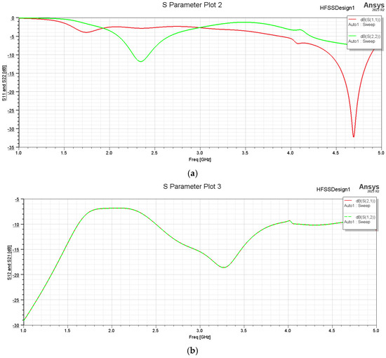
Figure 25.
The S parameters for the MIMO antennas considering the optimum structure of the key antenna: (a) S11 and S22; (b) S12 and S22.
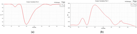
Figure 26.
The parameters used to characterize the MIMO antenna obtained from the key antenna: (a) ECC; (b) DG.
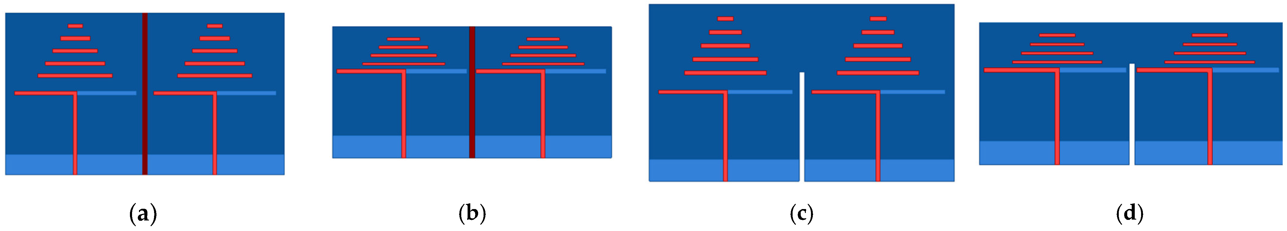
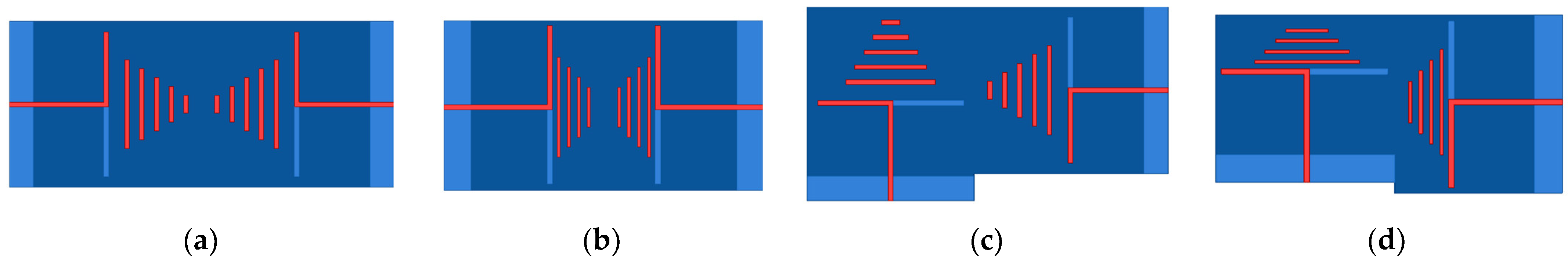
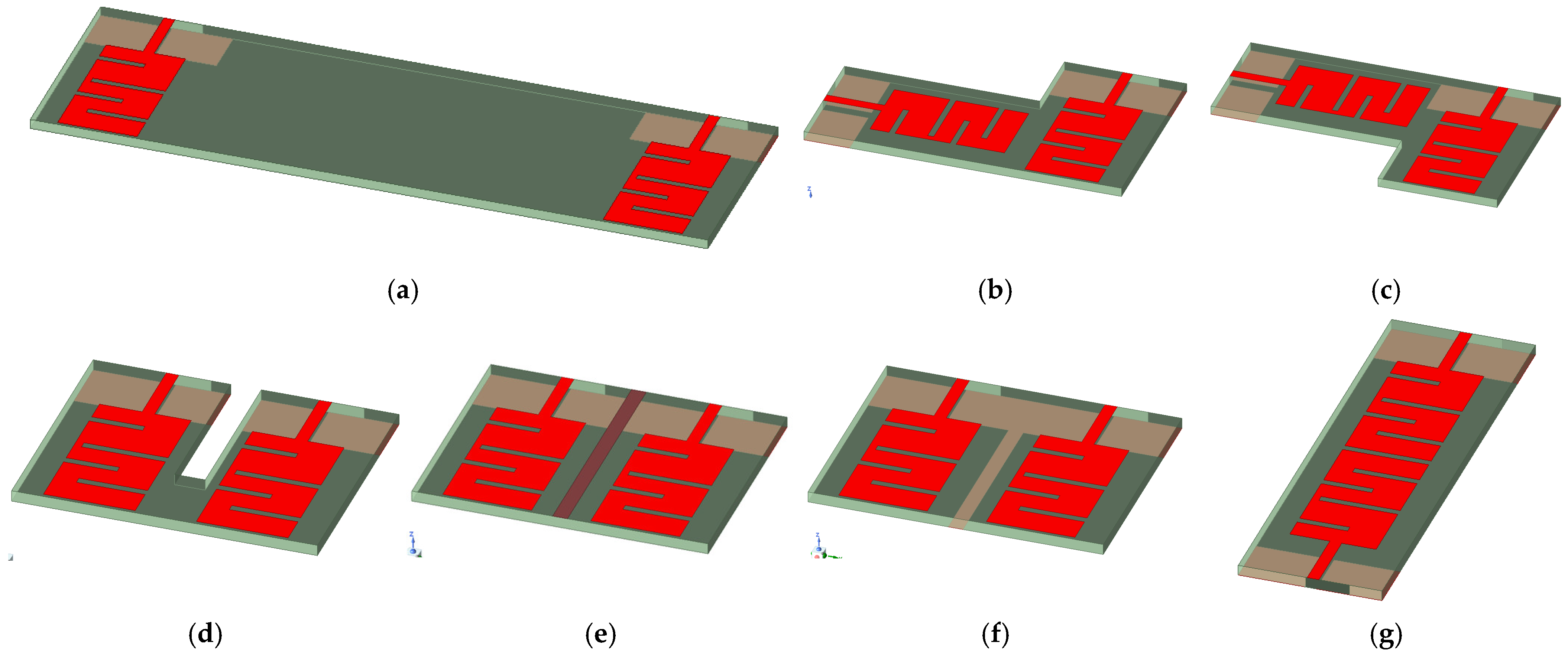
Figure 27 displays all of the structures considered for this study. The design process began by increasing the distance between the antennas to λ/2, followed by experimenting with antenna shifts at different angles (90° and 180°), inserting a metallic strip between the antennas, and creating a slot between them.

Figure 27.
The structures considered for increasing the efficiency of the MIMO structure: (a) antennas at λ/2; (b) antennas at 90° up; (c) antennas at 90° down; (d) antennas with slot; (e) antennas with metallic strip between them on the upper surface of the dielectric; (f) antennas with metallic strip between them on the upper surface of the dielectric; (g) antennas at 180°.
5. Discussion
MIMO antennas operating at 2.4 GHz are used in a variety of applications, from wireless local area networks [27] and IoT (Internet of Things) applications [28] to unmanned aerial vehicles (UAV) and RF energy harvesting systems [29]. Their strong point is their high data transfer, signal reliability, and spectral efficiency, which can be achieved only if the antennas are constructed in an efficient manner. Thus, their coupling is verified constantly to achieve a structure that is as small as possible while still allowing for the desired functioning. In this study, we analyzed a larger-scale antenna and a smaller one, pointing out that their efficiency was based on the geometry and different decoupling methods and could be determined only by analyzing each structure and its characteristics separately.
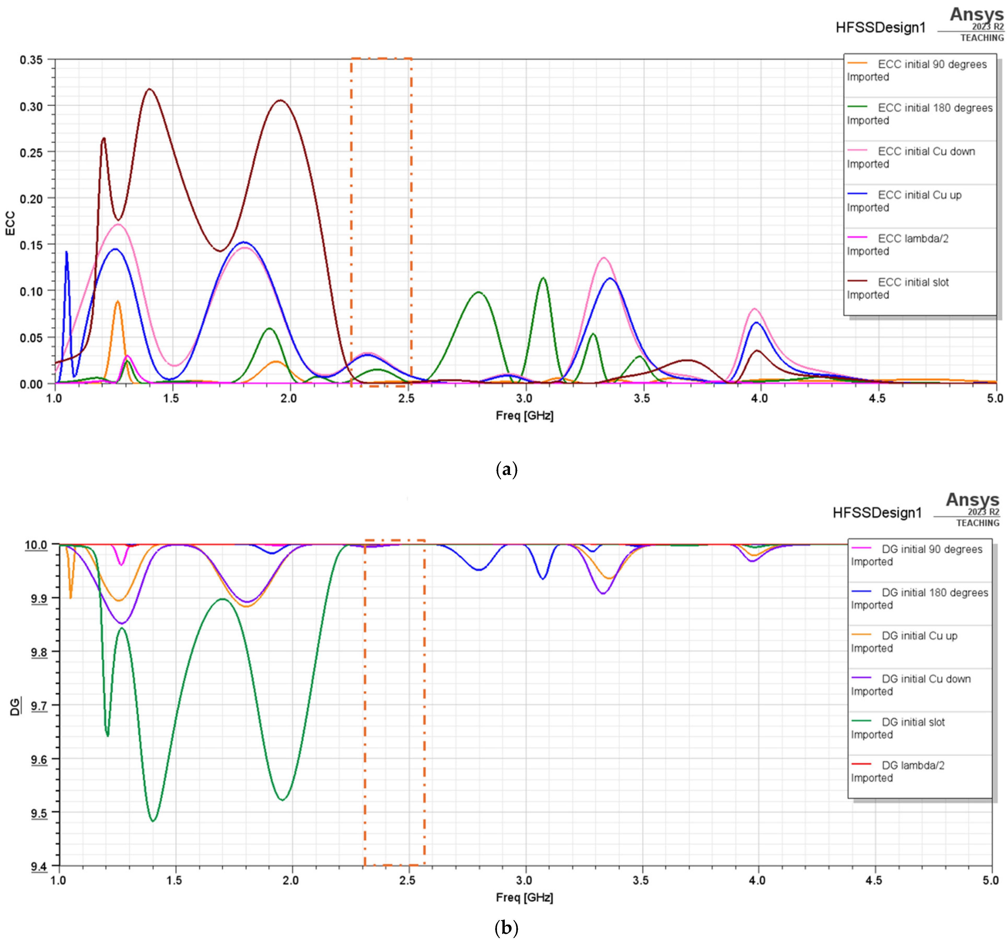
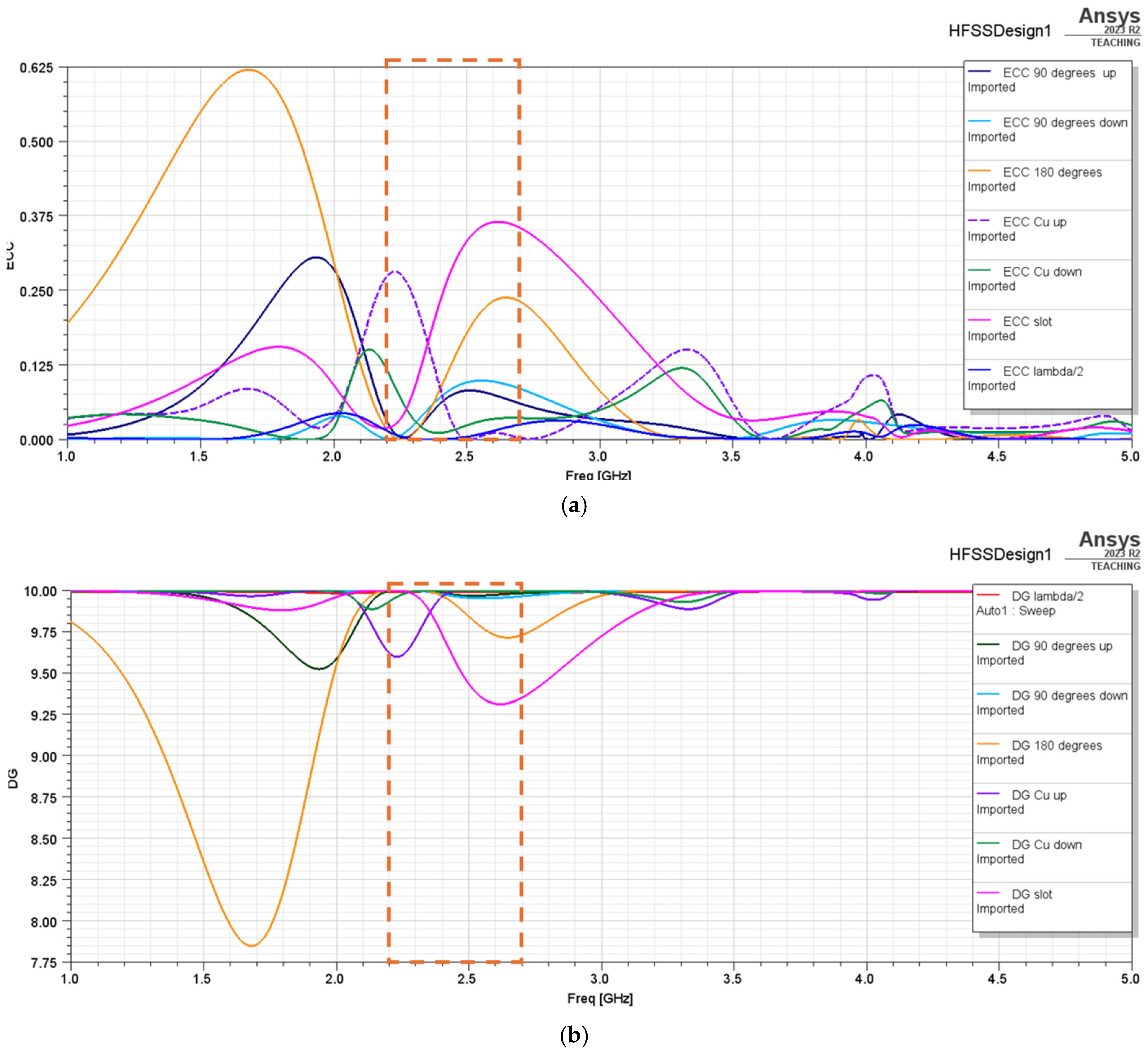
After analyzing all of the structures mentioned above for the Yagi–Uda antenna, the ECC and DG graphs were determined for the initial structure (Figure 28). It can be seen that in the bandwidth where the antenna was operating presented in the figure inside the orange rectangle, all of the methods used produced great results when considering the parasitic interference reduction. The best result was, as expected, the one for the distance of half of the wavelength between the antennas, followed by the method where the antennas were placed at an angle of 90°. Introducing a slot between the antennas was also effective but only in this bandwidth, because for lower frequencies it was the least efficient of the methods considered.
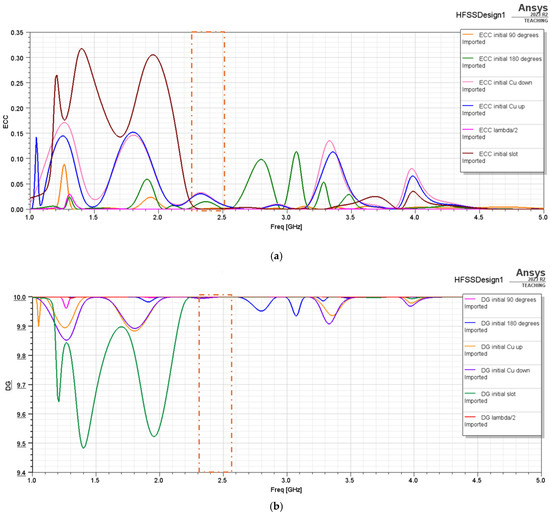
Figure 28.
The parameters used to characterize the MIMO antenna obtained from the Yagi-Uda antenna on which decoupling methods were implemented: (a) ECC; (b) DG.
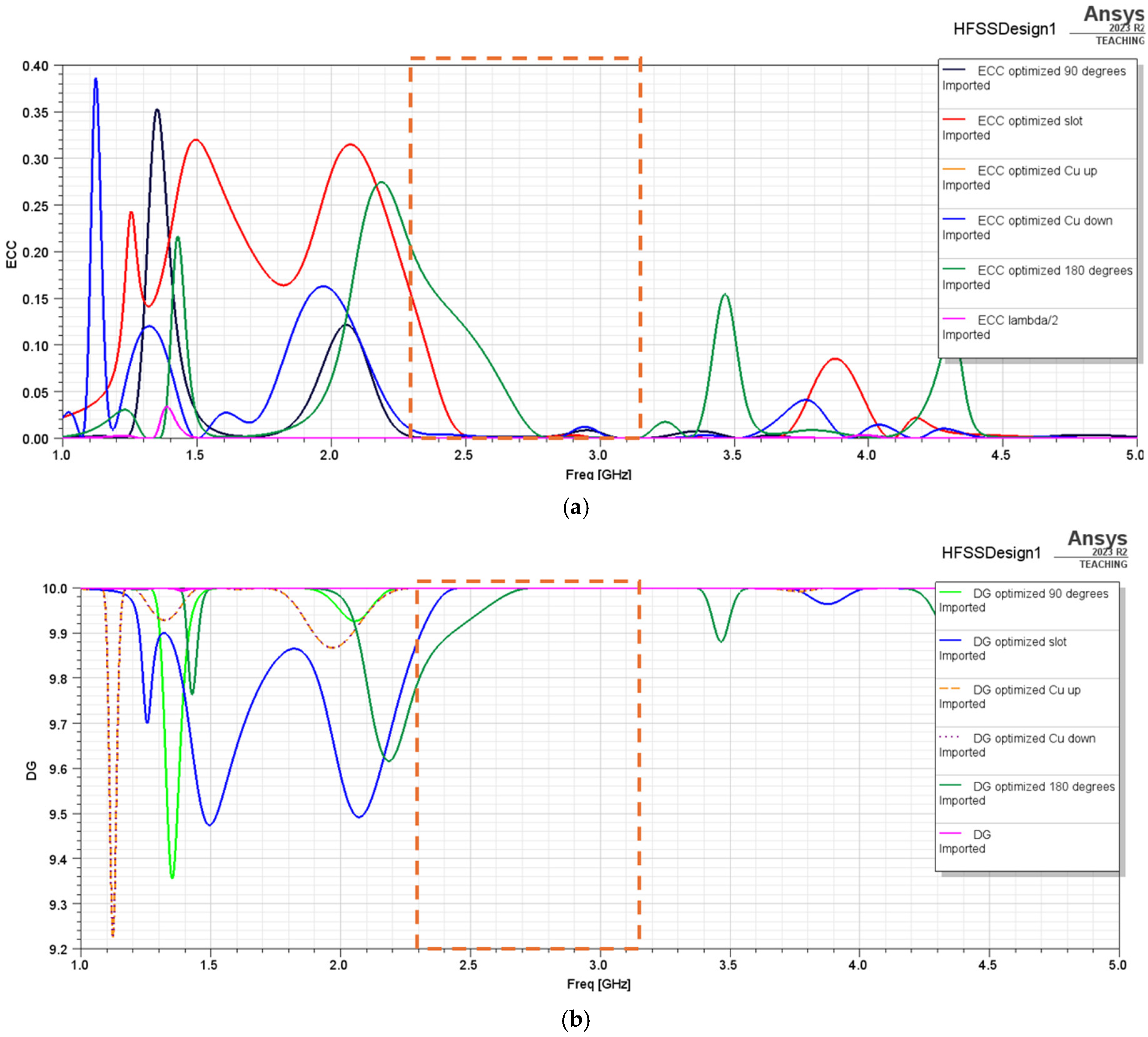
For the optimized structure, the ECC and DG graphs were also determined (Figure 29). For this case, the methods were also effective, but inserting the slot and placing the antennas at 180° from each other were the least effective at around 2.4–2.6 GHz, the frequency at which we wanted the antenna to function. Also, in this case, the ECC tended to reach even higher values in the frequency range analyzed. The effectiveness of the methods can also be observed by analyzing the S parameters of the structures, which tended to overlap and to have the same bandwidth as the initial optimized structure for the Yagi–Uda planar antenna. The orange rectangle includea, as in the previous case, the bandwidth of the analyzed antenna.
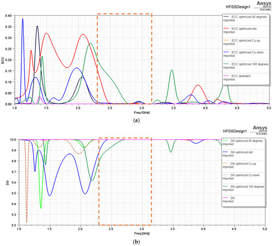
Figure 29.
The parameters used to characterize the MIMO antenna from the optimized structure: (a) ECC; (b) DG.
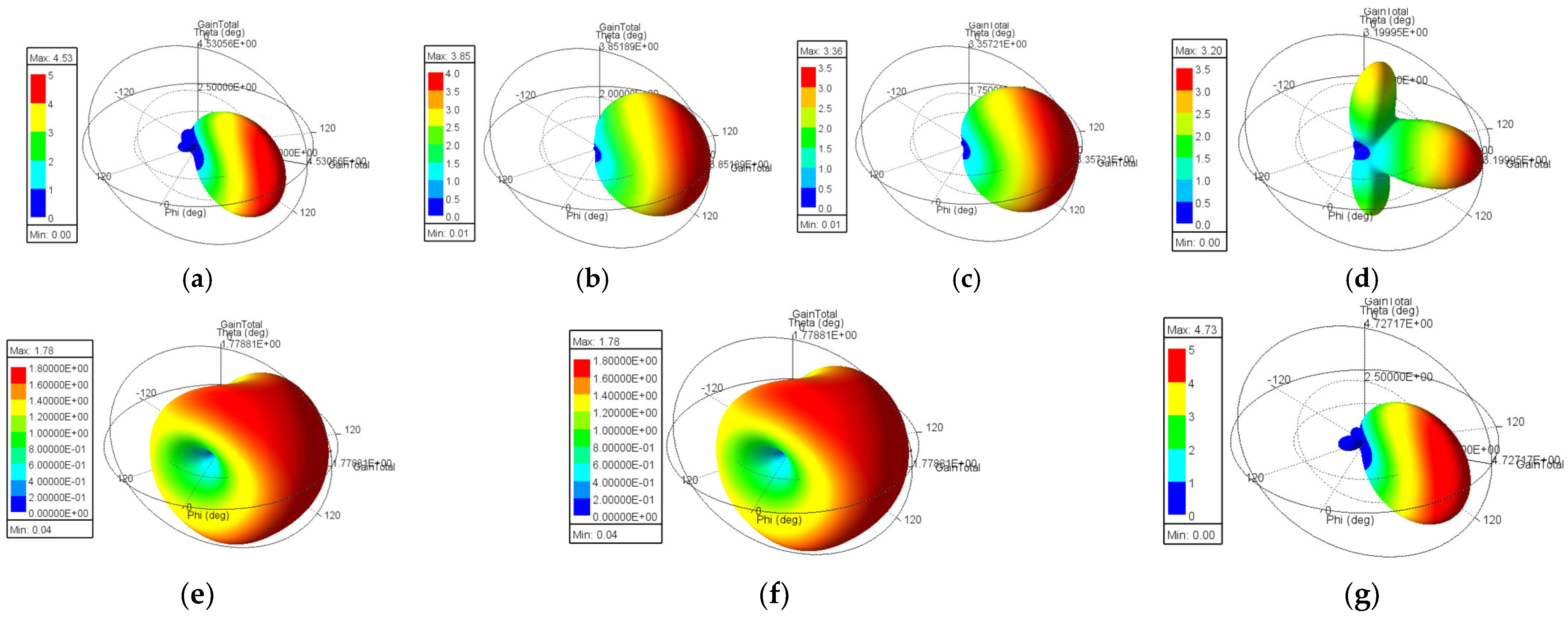
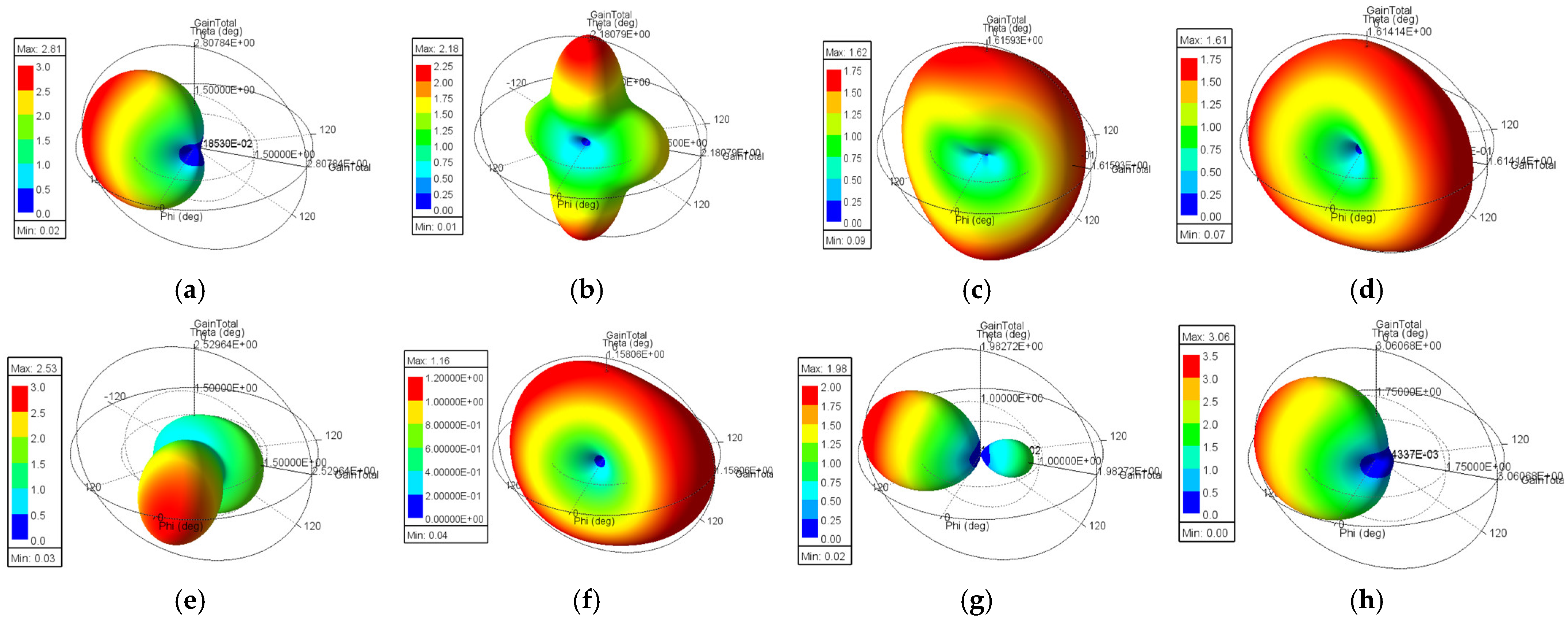
For the different MIMO structures, the 3D polar plot was also obtained in order to see how the different decoupling methods affected the way in which the antenna radiated (Figure 30). The initial antenna radiated in a unidirectional manner, and a lot of MIMO structures radiate in the same way. Differences appeared when considering the antennas shifted by 180° where three lobes were present and in the case where copper was inserted between the antennas, where the structure tended to radiate in an omnidirectional manner. The highest values of the peak gain were found in the case where the antennas were next to each other and when a slot was inserted between them.
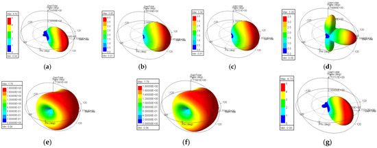
Figure 30.
2D polar gain plot for the considered MIMO structures for the optimized Yagi–Uda antenna: (a) next to each other; (b) placed at half wavelength; (c) at 90°; (d) at 180°; (e) copper strip up; (f) copper strip down; (g) slot.
While for the Yagi–Uda antenna there were no large differences in the studied frequency domain of the antenna and all of the methods were effective, in the case of the second antenna, the key antenna, not all of the methods gave the expected results (Figure 31). The best of the methods was the one where the antennas were placed at half wavelength from each other in the MIMO structure. The next best structure was the one with the metallic strip placed under the dielectric as a continuation of the ground plane and with the antennas placed at 90° from each other. The slot and placing the antennas at 180° from each other were the worst of the methods used. Analyzing the DG graph, the same conclusions can be drawn.
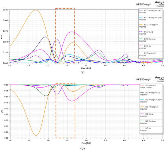
Figure 31.
The parameters used to characterize the MIMO antenna obtained from the key antenna on which decoupling methods were implemented: (a) ECC; (b) DG.
Thus, considering these results, one must conclude that the best decoupling methods were not the same for each antenna considered, and that decreasing the dimensions of an antenna will lead to more parasitic effects that must be avoided in MIMO structures.
When considering the 2D polar plots for the gain, it can be observed that only the structures with the copper strip placed over the dielectric between the antennas and the structures where the antennas were placed at 90° from each other maintained the shape of the radiation, while the highest gain values were obtained for the MIMO antenna with a slot and the one with the antennas placed at 180° from each other (Figure 32).
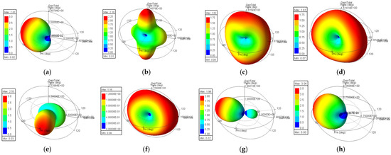
Figure 32.
2D polar gain plot for the considered MIMO structures for the key antenna: (a) next to each other; (b) placed at half wavelength; (c) at 90° up; (d) at 90° down; (e) at 180°; (f) copper strip up; (g) copper strip down; (h) slot.
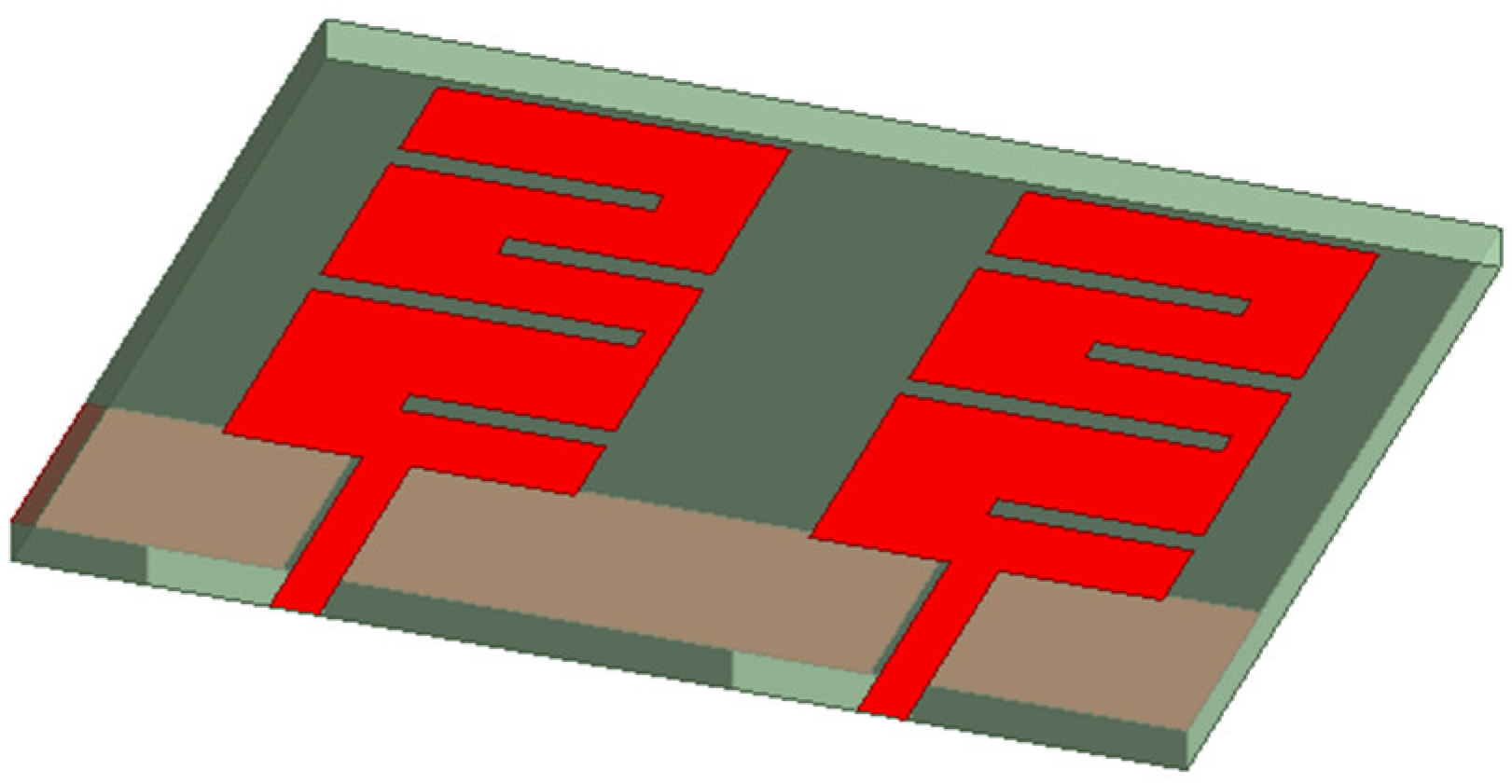
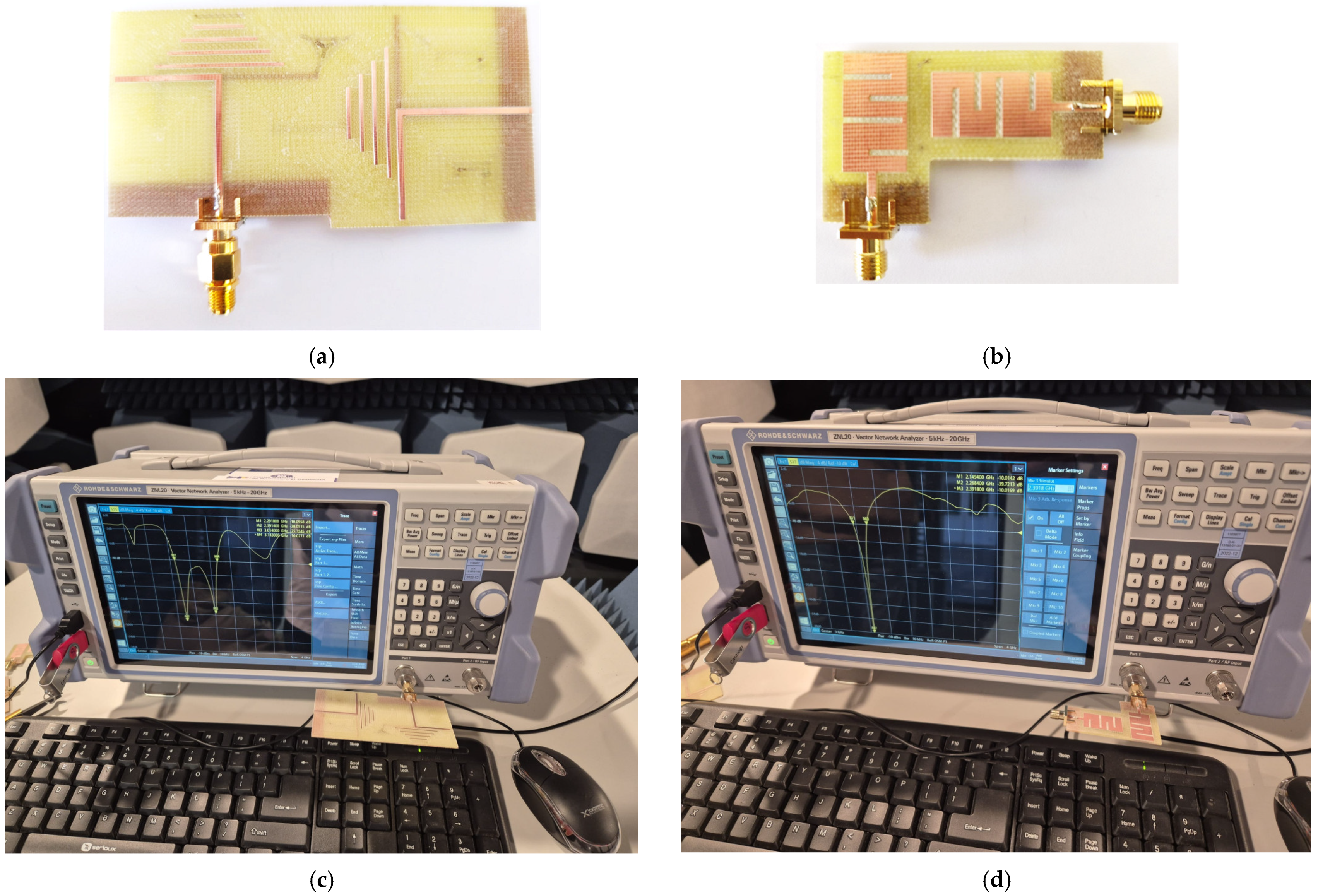
Some of the MIMO antennas, namely the optimized antenna for the first configuration and the second antenna, are presented along with the measurement of the S parameters in Figure 33.
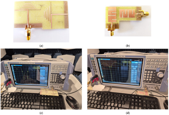
Figure 33.
The two-antenna MIMO constructed and measured: (a) first structure optimized; (b) second antenna; (c) measurement of the S parameters for the first structure considered; (d) measurement of the S parameters for the second structure considered.
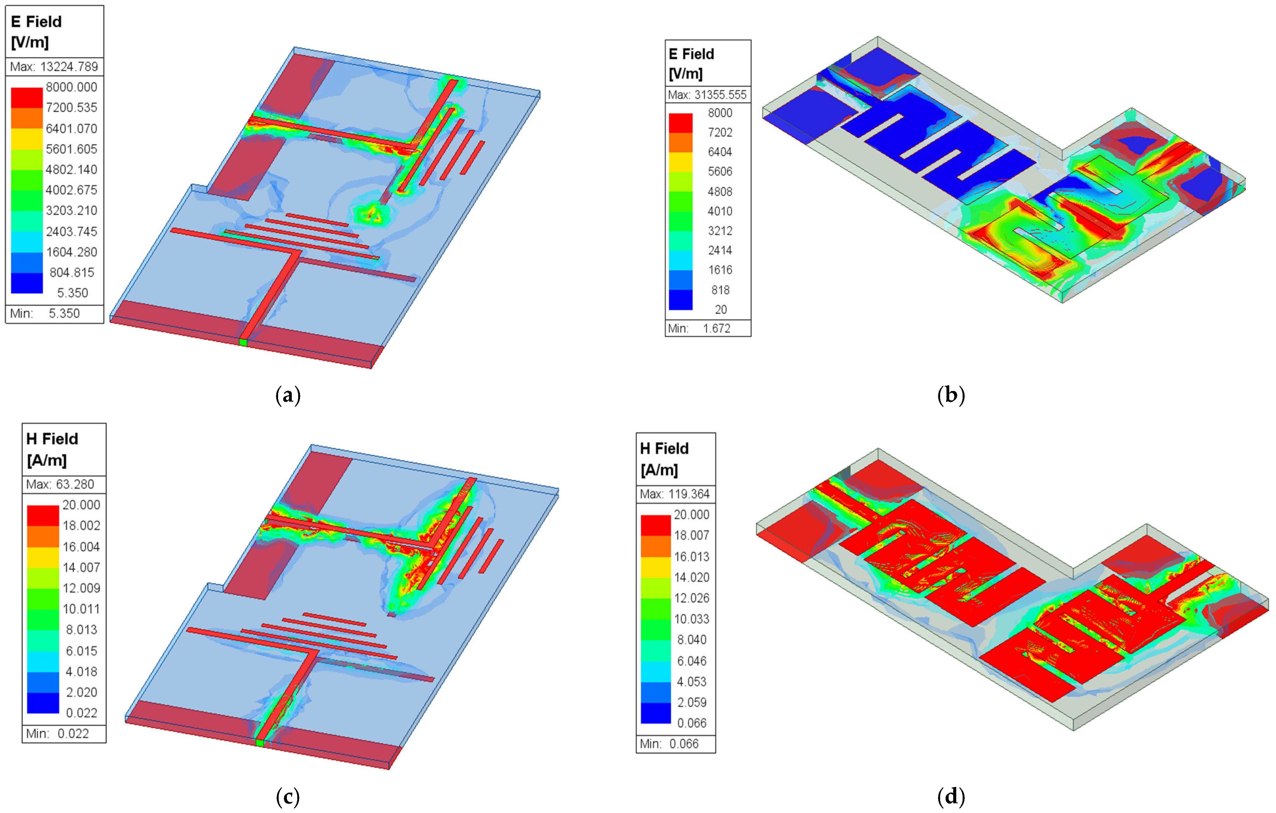
To provide a clearer understanding of the coupling effect, we also analyzed the electric and magnetic fields [30] in the two optimized structures, as shown in Figure 34. The electric field intensity in the second optimized MIMO structure was approximately three times higher than in the first optimized structure. This was particularly evident in the region between the two antennas, where the elevated electric field values indicated stronger coupling. Additionally, the second structure exhibited a larger surface area on the dielectric with high electric field intensity, further confirming the increased coupling effect. The same thing could be observed when analyzing the two structures from the magnetic field point of view, where the maximum values of the magnetic field were almost two times higher in the second optimized MIMO structure than in the first optimized structure.

Figure 34.
Electric and magnetic field of the two optimized MIMO antennas: (a) electric field in the first antenna; (b) electric field in the second antenna; (c) magnetic field in the first antenna; (d) magnetic field in the second antenna.
6. Conclusions
This study explored the design and optimization of two antenna structures operating at 2.4 GHz, followed by an investigation into various parasitic element suppression techniques when integrated into MIMO configurations. The optimization of both antennas focused on reducing their dimensions while maintaining efficient performance at the target frequency. Several decoupling methods, including adjusting the antenna placement, introducing metallic strips, and incorporating slots, were employed to mitigate the mutual coupling and enhance the isolation between the antennas.
The different decoupling techniques demonstrated varying degrees of success in reducing the ECC and improving the DG, though some techniques required trade-offs in the antenna dimensions or complexity. Also, the influence of such methods on the gain of the MIMO structures is presented. For the structures analyzed and the bandwidths where they operate, the best decoupling technique is considered placing them at half wavelength from each other, but the structure’s dimensions are greatly increased. This is why, if we needed to choose one method, this would be the second best, namely placing the antennas at an angle of 90° from each other, which completely decouples the initial Yagi–Uda antennas, while for the other two antenna structures, decoupling is improved but the method is not that effective considering the S parameters, the ECC, and the DG.
This study highlights the importance of carefully selecting the decoupling methods to achieve the optimal performance in MIMO systems, particularly in reducing the parasitic effects that can degrade the system’s performance.
Author Contributions
Conceptualization, C.C., C.P., A.G. and C.M.; methodology, C.C., A.G., L.G. and C.P.; validation, C.C., A.G., C.P., L.G., M.G. and S.A.; formal analysis, C.C.; investigation, C.C., C.P., A.G. and C.M.; resources, S.A. and M.G.; data curation, C.C., C.P., A.G. and C.M.; writing—original draft preparation, C.C.; writing—review and editing, C.C., A.G., L.G. and C.P.; visualization, S.A. and M.G.; supervision, C.M.; project administration, C.C.; funding acquisition, C.C. All authors have read and agreed to the published version of the manuscript.
Funding
This research was funded by the Technical University of Cluj-Napoca, grant number 18/01.07.2024.
Institutional Review Board Statement
Not applicable.
Informed Consent Statement
Not applicable.
Data Availability Statement
Data is contained within the article.
Acknowledgments
This work was supported by the “Dezvoltarea și optimizarea antenelor MIMO și evaluarea expunerii umane la radiațiile emise de acestea” (“Development and Optimization of MIMO Antennas and Evaluation of Human Exposure to the Radiation Emitted by Them”) grant funded by the National Grant Competition—GNaC ARUT 2023.
Conflicts of Interest
The authors declare no conflicts of interest.
Abbreviations
The following abbreviations are used in this manuscript:
| ECC | Envelope correlation coefficient |
| DG | Diversity gain |
| VNA | Vector network analyzer |
| MIMO | Multiple input multiple output |
| HFSS | High Frequency Structure Simulator |
References
- Jayant, S.; Srivastava, G.; Kumar, S.; Mostafa, H.; Goyal, B.; Choi, H.C.; Kim, K.W. Decoupling Methods in Planar Ultra-Wideband Multiple-Input-Multiple-Output Antennas: A Review of the Design, State-of-the-Art, and Research Challenges. Electronics 2023, 12, 3813. [Google Scholar] [CrossRef]
- Ibrahim, S.K.; Singh, M.J.; Al-Bawri, S.S.; Ibrahim, H.H.; Islam, M.T.; Islam, M.S.; Alzamil, A.; Abdulkawi, W.M. Design, Challenges and Developments for 5G Massive MIMO Antenna Systems at Sub 6-GHz Band: A Review. Nanomaterials 2023, 13, 520. [Google Scholar] [CrossRef]
- Ahmed, M.; Zafar, Z.; Javed, I.; Zahid, M.; Amin, Y. 12 Element Inverted E-Shaped Massive MIMO Antennas for Future 5G Smartphone Applications. In Proceedings of the 2023 7th International Multi-Topic ICT Conference (IMTIC), Jamshoro, Pakistan, 10–12 May 2023; pp. 1–5. [Google Scholar] [CrossRef]
- Musaed, A.A.; Al-Bawri, S.S.; Abdulkawi, W.M.; Aljaloud, K.; Yusoff, Z.; Islam, M.T. High isolation 16-port massive MIMO antenna based negative index metamaterial for 5G mm-wave applications. Sci. Rep. 2024, 14, 290. [Google Scholar] [CrossRef]
- Tiwari, R.N.; Singh, P.; Kanaujia, B.K.; Srivastava, K. Neutralization technique based two and four port high isolation MIMO antennas for UWB communication. AEU-Int. J. Electron. Commun. 2019, 110, 152828. [Google Scholar] [CrossRef]
- Zhang, S.; Pedersen, G.F. Mutual Coupling Reduction for UWB MIMO Antennas with aWideband Neutralization Line. IEEE Antennas Wirel. Propag. Lett. 2015, 15, 166–169. [Google Scholar] [CrossRef]
- Arumugam, S.; Manoharan, S.; Palaniswamy, S.K.; Kumar, S. Design and Performance Analysis of a Compact Quad-Element UWB MIMO Antenna for Automotive Communications. Electronics 2021, 10, 2184. [Google Scholar] [CrossRef]
- Govindan, T.; Palaniswamy, S.K.; Kanagasabai, M.; Kumar, S. Design and Analysis of UWB MIMO Antenna for Smart Fabric Communications. Int. J. Antennas Propag. 2022, 2022, 5307430. [Google Scholar] [CrossRef]
- Jayant, S.; Srivastava, G.; Kumar, S. Quad-Port UWB MIMO Footwear Antenna for Wearable Applications. IEEE Trans. Antennas Propag. 2022, 70, 7905–7913. [Google Scholar] [CrossRef]
- Azarm, B.; Nourinia, J.; Ghobadi, C.; Majidzadeh, M. Highly isolated dual band stop two-element UWB MIMO antenna topology for wireless communication applications. J. Instrum. 2019, 14, P10036. [Google Scholar] [CrossRef]
- Tang, Z.; Wu, X.; Zhan, J.; Hu, S.; Xi, Z.; Liu, Y. Compact UWB-MIMO Antenna with High Isolation and Triple Band-Notched Characteristics. IEEE Access 2019, 7, 19856–19865. [Google Scholar] [CrossRef]
- Amin, F.; Saleem, R.; Shabbir, T.; Rehman, S.U.; Bilal, M.; Shafique, M.F. A Compact Quad-Element UWB-MIMO Antenna System with Parasitic Decoupling Mechanism. Appl. Sci. 2019, 9, 2371. [Google Scholar] [CrossRef]
- Ren, J.; Hu, W.; Yin, Y.; Fan, R. Compact Printed MIMO Antenna for UWB Applications. IEEE Antennas Wirel. Propag. Lett. 2014, 13, 1517–1520. [Google Scholar]
- Li, Z.; Yin, C.; Zhu, X. Compact UWB MIMO Vivaldi Antenna with Dual Band-Notched Characteristics. IEEE Access 2019, 7, 38696–38701. [Google Scholar] [CrossRef]
- Jansari, D.V.; Amineh, R.K. A two-element antenna array for compact portable MIMO-UWB communication systems. AIMS Electron. Electr. Eng. 2019, 3, 224–232. [Google Scholar] [CrossRef]
- Jayant, S.; Srivastava, G. Close-Packed Quad-Element Triple-Band-Notched UWB MIMO Antenna with Upgrading Capability. IEEE Trans. Antennas Propag. 2022, 71, 353–360. [Google Scholar] [CrossRef]
- Kumar, S.; Lee, G.H.; Kim, D.H.; Mohyuddin, W.; Choi, H.C.; Kim, K.W. Multiple-input-multiple-output/diversity antenna with dual band-notched characteristics for ultra-wideband applications. Microw. Opt. Technol. Lett. 2019, 62, 336–345. [Google Scholar] [CrossRef]
- Kumar, S.; Lee, G.H.; Kim, D.H.; Mohyuddin, W.; Choi, H.C.; Kim, K.W. A compact four-port UWB MIMO antenna with connected ground and wide axial ratio bandwidth. Int. J. Microw. Wirel. Technol. 2019, 12, 75–85. [Google Scholar] [CrossRef]
- Constantinescu, C.; Pacurar, C.; Giurgiuman, A.; Munteanu, C.; Andreica, S.; Gliga, M. High Gain Improved Planar Yagi Uda Antenna for 2.4 GHz Applications and Its Influence on Human Tissues. Appl. Sci. 2023, 13, 6678. [Google Scholar] [CrossRef]
- Dong, K.; Zhang, F.S.; Chen, L.; Zhu, P.; Zhang, Q.; Zhu, Y. A compact dual-band planar monopole antenna for 2.4/5 GHz WLAN application. In Proceedings of the 2010 International Symposium on Signals, Systems and Electronics, Nanjing, China, 17–20 September 2010; pp. 1–4. [Google Scholar] [CrossRef]
- Awan, W.A.; Islam, T.N.; Alsunaydih, F.; Alsaleem, F.; Alhassoonc, K. Dual-band MIMO antenna with low mutual coupling for 2.4/5.8 GHz communication and wearable technologies. PLoS ONE 2024, 19, e0301924. [Google Scholar] [CrossRef]
- Cheng, Y.-F.; Cheng, K.-K.M. Decoupling of 2 × 2 MIMO Antenna by Using Mixed Radiation Modes and Novel Patch Element Design. IEEE Trans. Antennas Propag. 2021, 69, 8204–8213. [Google Scholar] [CrossRef]
- Ridha, O.; Boutayeb, H.; Louati, S. TE50 Mode SIW Waveguide-Fed Yagi Antenna Array Operating at 5.8 GHz. In Proceedings of the 2024 International Conference on Computing, Internet of Things and Microwave Systems (ICCIMS), Gatineau, QC, Canada, 29–31 July 2024; pp. 1–5. [Google Scholar] [CrossRef]
- Ahmad, J.; Hashmi, M.; Bakytbekov, A.; Falcone, F. Design and Analysis of a Low Profile Millimeter-Wave Band Vivaldi MIMO Antenna for Wearable WBAN Applications. IEEE Access 2024, 12, 70420–70433. [Google Scholar] [CrossRef]
- Gad, M.M.; Sallam, M.O. High gain antipodal meander line antenna for point-to-point WLAN/WiMAX applications. Sci. Rep. 2024, 14, 5769. [Google Scholar] [CrossRef]
- Constantinescu, C.; Andreica, S.; Laszlo, R.; Giurgiuman, A.; Gliga, M.; Munteanu, C.; Pacurar, C. Numerical Modeling, Analysis, and Optimization of RFID Tags Functioning at Low Frequencies. Appl. Sci. 2024, 14, 9544. [Google Scholar] [CrossRef]
- Kim, J.; Shin, H.; Wi, S.; Lee, H.; Li, R.; Kim, H. 2 × 2 MIMO dual-wideband ground radiation antenna with a T-shaped isolator for Wi-Fi 6/6E/7 applications. Sci. Rep. 2025, 15, 85. [Google Scholar] [CrossRef] [PubMed]
- Anouar Es-saleh, Mohammed Bendaoued, Soufian Lakrit, Sudipta Das, Ahmed Faize, Design aspects of MIMO antennas and its applications: A comprehensive review. Results Eng. 2025, 25, 103797. [CrossRef]
- Kumar, A.; Narayaswamy, N.K.; Kumar, H.V.; Mishra, B.; Siddique, S.A.; Dwivedi, A.K. High-isolated WiFi-2.4 GHz/LTE MIMO antenna for RF-energy harvesting applications. AEU—Int. J. Electron. Commun. 2021, 141, 153964. [Google Scholar] [CrossRef]
- Gu, Z.; Ma, Q.; Gao, X.; You, J.W.; Cui, T.J. Direct electromagnetic information processing with planar diffractive neural network. Sci. Adv. 2024, 10, eado3937. [Google Scholar] [CrossRef]


Disclaimer/Publisher’s Note: The statements, opinions and data contained in all publications are solely those of the individual author(s) and contributor(s) and not of MDPI and/or the editor(s). MDPI and/or the editor(s) disclaim responsibility for any injury to people or property resulting from any ideas, methods, instructions or products referred to in the content. |
© 2025 by the authors. Licensee MDPI, Basel, Switzerland. This article is an open access article distributed under the terms and conditions of the Creative Commons Attribution (CC BY) license (https://creativecommons.org/licenses/by/4.0/).