Abstract
This article proposes a compact model for the radiation-sensitive field-effect transistor (RADFET). The model represents the basic I–V characteristics of the MOSFET device and includes the effects of threshold voltage shift as a function of absorbed dose and gate bias, gate tunneling current, gate radiation current, dose accumulation, and fading. It accurately represents high-field effects in the gate dielectric of the RADFET device. Both the Fowler–Nordheim gate tunneling current and the radiation-induced gate current are incorporated into the model. The model enables determination of the radiation-induced charge during RADFET operation under high-field injection conditions, thereby improving the precision of accumulated dose readout. The proposed model is fully compatible with SPICE-based circuit simulators and can represent any type of RADFET device, including those with high-k gate dielectrics. Furthermore, the model was developed entirely using open-source circuit simulation tools.
1. Introduction
Radiation-sensitive field-effect transistors (RADFETs) are widely used for ionizing radiation monitoring in applications such as aerospace systems, nuclear installations, dosimetry instruments, radiation therapy, and environmental monitoring [1,2,3]. Typically, p-channel metal-oxide-semiconductor field-effect transistors (PMOSFETs) are employed as RADFET devices. The radiation-induced charge accumulated in the gate dielectric of the MOSFET causes a shift in the threshold voltage [4,5,6]. By calibrating the dependence of the shift on the accumulated dose, it is possible to determine the absorbed dose from the measured value [1,6,7]. RADFET sensors offer several advantages, including a small active area, low cost, and simple readout circuitry [8,9]. Furthermore, RADFET sensors can be integrated into integrated circuits (ICs) to define the device operating point and enable efficient readout processing [10].
Improving dose sensitivity and utilizing standard CMOS technology nodes such as CD4000 represent key development directions for RADFET sensors [11,12,13]. Such RADFET sensors typically operate under positive gate bias. This operating mode accelerates the separation of electron-hole pairs generated during device irradiation and increases the radiation-induced charge accumulated in the gate dielectric [14,15,16]. The dose sensitivity of the RADFET device and the charge work function both increase with the electric field in the gate dielectric. The operation of MOS sensors under high electric fields in the gate dielectric, particularly under Fowler–Nordheim tunneling conditions, is of special interest [17,18,19]. The use of high-field electron tunneling enables injection annealing after irradiation [17,19,20]. Our research team has proposed a model describing the charge processes in MOS sensors under various gate biases, extending up to the high-field injection region [21,22]. The proposed model can also describe the annealing process [23,24]. Integrating this mathematical model into SPICE-compatible circuit simulation software would enhance its accessibility. The RADFET SPICE models would be particularly useful for the design of specialized integrated circuits (ICs). Moreover, the SPICE RADFET model could be applied in the design of radiation-hardened ICs, enabling consideration of MOSFET parameter shifts caused by irradiation.
SPICE-based circuit simulation tools [25] are the industrial standard for electronic circuits modelling. The most of proprietary (HSPICE, LTspice) and open source (Ngspice, Xyce) circuit simulation tools are based on original SPICE code developed by L.Nagel. The SPICE simulation kernel supports a set of basic passive and active primitive devices, including resistors, inductors, sources, and transistors. The electronic components not included in a basic set of SPICE devices should be described using macromodels or compact models [26]. The macro model represents a complex device as an equivalent circuit. A compact models differs from a macro model by using only simple devices like controlled sources and RCL components in the equivalent circuit. The electronic components are represented by a set of equations describing the voltages and current at its terminals. There are two ways of compact models integration in circuit simulation software:
- Using SPICE subcircuits (.SUBCKT directive) or macromodels [27]. The compact model is assembled as a set of primitive devices (resistor, capacitor, inductor) and behavioral (B-type) sources representing current on voltage or voltage on current dependencies. This method is supported by every SPICE simulation kernel, but complex models may have a poor performance, because the model parsing is required every time when netlist is loaded.
- Using Verilog-A hardware description language [28]. The Verilog-A is an extension of Verilog for analog circuits. The Verilog-A models are compiled into binary shared objects that could be attached to the simulator at the execution time. Therefore Verilog-A provides a better performance than subcircuits.
- Using XSPICE extensions [29,30]. XSPICE modules are written in C programming language with macros and also compiled as shared objects. XSPICE extension are much more difficult to design, but allows to provide a more deep integration of the model and simulation kernel. XSPICE brings no benefit for RADFET model because of design difficulties and no possibility of direct export from schematic. The deep integration with SPICE simulation kernel provided by XSPICE is not required for RADFET device compact model.
In summary, the compact model of the RADFET device can be implemented either as a subcircuit or in Verilog-A form. The Verilog-A implementation is generally preferable, as it offers higher performance. However, since Verilog-A is not supported by some SPICE simulation kernels, such as LTSpice, the subcircuit-based approach provides greater flexibility and broader compatibility.
The RADFET device is not included among the standard SPICE components, which creates a need to develop a custom model. Such a model would enable accurate simulation of the analog part of dosimeter readout circuits using SPICE-compatible circuit simulation tools. The study presented in [31] proposes a modification of the standard SPICE MOSFET model, where the radiation input is represented as a subcircuit parameter. However, this approach has certain limitations, as it employs only a simplified dependence of the MOSFET threshold voltage shift on the absorbed dose. The objective of this research is to extend the model presented in [31] by incorporating additional effects such as gate tunneling current, threshold voltage shift under irradiation, and fading. These improvements are essential for accurate simulation of analog circuits containing RADFET devices. The work described in [32] introduces a limited compact model of the RADFET device but does not provide implementation details.
The novelty of the presented model, compared to the existing approach based on modifying the SPICE model card, lies in its ability to represent the accumulated dose as a virtual input signal (typically a voltage). This feature is not possible when the dose is introduced as a fixed model card parameter. Consequently, the proposed RADFET compact model enables advanced simulations of circuits that include RADFETs and allows for the estimation of dynamic properties such as fading. In addition, the custom compact model makes it possible to incorporate effects that are not represented in the standard SPICE MOSFET model, which would be difficult to achieve through model card modification alone.
In this article, “radiation” refers to ionizing radiation (for example X-rays, gamma-rays, protons etc.). The sensor and model were calibrated by a gamma-ray source.
The rest of the paper is organized as follows. Section 2 provides an overview of the RADFET device, software used for the model generation, and model equations. Section 3 presents the structure of the generated SPICE model and compares the data from simulation and measurement. Section 4 gives a model usage example for readout circuit design. Finally, Section 5 gives an outcome of the paper and the summary of the achieved results.
2. Materials and Methods
2.1. Used RADFET Device
The RADFET devices [21] were fabricated using the 6 m CMOS technology compatible with CD4000 logic IC series. The radiation sensor is shown in Figure 1. It consists of two RADFET devices placed in a single ceramic package. Every RADFET is a PMOS device with a channel length of m and a channel width of m. The n-type silicon wafer doped by phosphorus was used as the substrate. The silicon substrate has 4.5 Ohms per square resistance and <100> orientation. The gate dielectric is silicon dioxide with 100 nm thickness. The total device area is 1,600,000 m2. Micron technology and relatively thick gate dielectric is preferable for RADFET fabrication. The thinner gate dielectric gives the decrease in RADFET sensitivity [33]. The dielectric thickness higher that 100 nm makes sufficient more difficult to implement the Fowler–Nordheim injection mode [34,35].
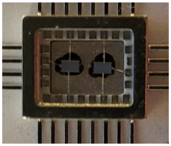
Figure 1.
Radiation sensor containing two PMOS RADFET devices.
The layout view of the RADFET device is shown in Figure 2. It uses multi finger topology to achieve large channel width and device area. Every RADFET has three electrodes: gate, drain and source. The independent gate pin allows to apply gate bias or gate injection current while the device irradiation.
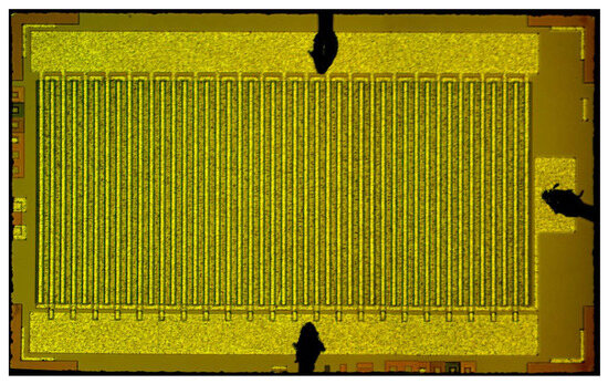
Figure 2.
RADFET device layout view.
2.2. Circuit Simulation Software
The Qucs-S circuit simulator (developed by Kuznetsov et al. [36]) was employed for the design of the presented compact model. This open-source tool offers several advantages: it is freely available, provides comprehensive functionality for compact model development, and includes advanced debugging capabilities that support efficient model verification and optimization. It provides access to SPICE directives, parameters, postprocessor directives and equations defined sources, which is needed to construct the compact model. By default Qucs-S uses free Ngspice [37] simulation kernel that is fully compatible with proprietary SPICE tools. There is a possibility to switch to XYCE circuit simulation backend or QucsatorRF backend specialized for RF simulation. Internal Verilog-A synthesizer of Qucs-S allows to export the designed compact model to Verilog-A module. Interactive tuning and optimization tools implemented in Qucs-S graphical user interface (GUI) level allow to perform models parameters extraction. The key feature of Qucs-S is the quick switching between the simulation backends while the program operation. Qucs-S uses external simulation kernel Ngspice [38] and Verilog-A [39] modules compiler OpenVAF. The data flow diagram is shown in Figure 3. It illustrates the interaction between the parts of the simulation software package.
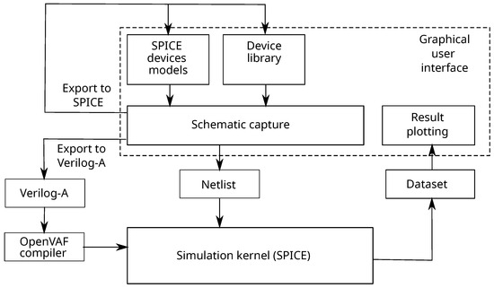
Figure 3.
Qucs-S dataflow diagram.
The main application is written using Qt6 framework and operates at the GUI level. The SPICE simulator and OpenVAF Verilog-A compiler are the command line (CLI) application. The communication between the GUI and CLI parts is implemented using the input and output files. The SPICE netlist is automatically generated and saved to file from the schematic view and serves as the input for SPICE backend. The Verilog-A modules could be specified before the simulation. The simulation backend produces a number of dataset files that could be parsed by visualization system of the main application to output graphs representing voltage and current waveforms and frequency domain response of the simulated circuit.
2.3. Basic RADFET Model Equations
All available SPICE simulators provide MOSFET models levels from 1 to 9 and advanced BSIM MOSFET models. The most of RADFET deices are fabricated using the micron technology. And the drain current could be described using MOSFET level 1 equations. MOSFET models levels above 3 and BSIM models [40], which have much more parameters and more complicated extraction procedure, are applicable for submicron devices and have no benefit for RADFET. MOSFET drain current depends on the voltages between the MOSFET pins: gate to source and and drain to source .
The drain current in the linear IV-curve region () is as follows:
where the is a threshold voltage (V); is channel modulation (1/V); and is transconductance ();
The drain current in the saturation region, if , is
The transconductance parameter as the model parameter should be distinguished from small signal transconductance parameter expressed in . The source of the RADFET device is internally connected to bulk, and the source-bulk voltage is . Therefore, the threshold voltage dependency on bulk potential may not be taken into account.
MOSFET threshold voltage and device transconductance have dependency on the device’s absolute temperature T (K) that must be taken into account in the module. The threshold voltage dependency may be approximated by the linear function
where the is the temperature where the initial device parameters could be measured and is a temperature coefficient (V/K). The transconductance temperature dependency may be approximated by the power function:
where is a coefficient varying in range from 1.3 to 1.5.
2.4. Radiation Dependency of the Threshold Voltage
The threshold voltage shift of the MOSFET can be considered linearly dependent on the absorbed dose D within certain limits. At higher absorbed doses, however, saturation effects become noticeable. The basic model assumes a simple linear dependence of the threshold voltage shift on the absorbed dose, expressed in rads or grays (Gy), without accounting for saturation effects. In this paper, dose values are expressed in rads:
where S is a sensitivity coefficient expressed in . The saturation of the threshold voltage shift at the higher dose may be expressed with a hyperbolic tangent. The more precise approximation proposed in [4,41] may cause convergence issues with SPICE simulator.
where is a dose at which saturation is reached. Usually rad.
The sensitivity has a complex dependency on gate bias during irradiation [42]. This dependency consists of linear and exponential terms:
where the and are the fitting coefficient. If the only the linear dependency on dose is taken into account.
2.5. Gate Current Model
The both MOSFET level 1–9 and BSIM model do not take into account gate current and radiation effects on gate current, which is important for RADFET operation. The gate current could be normalized to gate current density and gate area:
The gate current density of the RADFET device consists of three components: capacitive current , high-field tunnel injection current , and radiation current :
Capacitive component could be expressed using the known unity gate capacitance which may be expressed from gate dielectric parameters and gate oxide thickness :
where is a gate dielectric (for example, SiO2) permittivity and is a dielectric constant. The standard SPICE Level 1–9 MOSFET models used for micron-scale technologies do not provide a parameter for defining the gate dielectric permittivity.
The injection current could be expressed using the Fowler–Nordheim equations:
where is a barrier potential (V); and are Fowler–Nordheim tunneling constants.
The radiation current is expressed by the following Equation [21]:
where q is the charge of electron, is a value of electron-hole pair per dose unit and SiO2 volume (). The is the charge yield under irradiation. The charge yield is the fraction of holes that escape initial recombination [15]. This value measured in arbitrary units. It depends on the field E in the gate dielectric. The charge yield could be determined from the data provided by Schwank et al. [15]. We use the following approximation in the compact model:
where the and are the fitting constants depending on radiation type (gamma-ray, protons, etc.). The plots of the approximation function are shown in Figure 4. It shows good match with experimental plots from [15]. The typical values for and coefficients are given in Table 1.
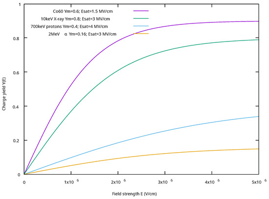
Figure 4.
Charge yield approximation.

Table 1.
Charge yield approximation coefficients.
3. Results
3.1. The Equivalent Circuit of the RADFET Device
The compact model represented by the following equivalent circuit designed in Qucs-S is shown in Figure 5 and Figure 6. For convenience of representation the schematic is splitted into two parts. The first part represents the drain current. The second part represents the gate model.
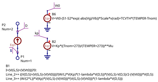
Figure 5.
The equivalent circuit representing the RADFET compact model: drain current stage.
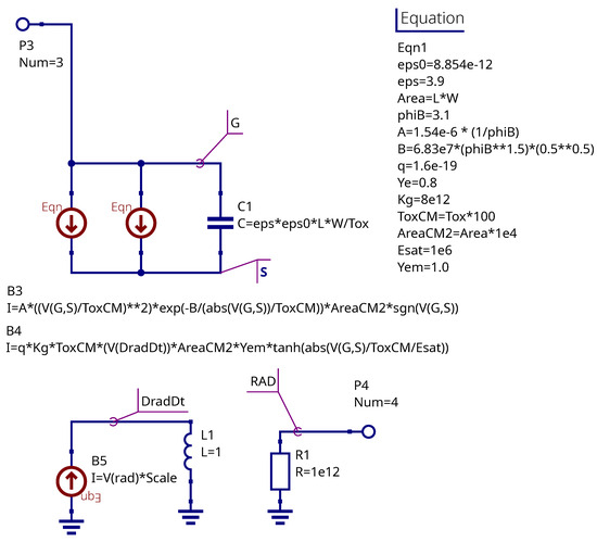
Figure 6.
The equivalent circuit representing the RADFET compact model: gate and radiation input.
The equivalent circuit consists of a number of behavioral current and voltage sources and equation defined passive devices. The model has three terminals for MOSFET electrodes: gate (G—port P3), source (S—port P1), and drain (D—port P2). The fourth terminal (RAD—port P4) serves as the virtual radiation input. The voltage source representing the absorbed dose in rads should be connected to this terminal. The input voltage at the RAD terminal is a virtual signal, and this input is excluded from the operation conditions check (OCC). The unit scale on this input could be set using the Scale model parameter. Set Scale = 1 for 1 V = 1 rad, or Scale = 1000 for 1 V = 1 krad. The dose D is related to the voltage at the radiation input as follows:
The Equation block in Figure 6 represents the parameters calculated before the simulation using the subcircuit parameters. This block is mapped to .PARAM block in the SPICE netlist. The B1 source represents the drain current level 1 MOSFET model with Equations (1) and (2).The transconductance parameter is represented as the virtual voltage. The B2 source is responsible for transconductance temperature dependency (4). The B3 and B4 current sources represent the gate injection (12) and radiation (13) currents respectively. The capacitor C1 is the gate capacitance (11). The L1 inductor and B5 source are a differentiation stage and serve to obtain the radiation intensity using the fundamental properties of inductor current. The B6 controlled source represents a threshold voltage shift dependency on the absorbed dose taking into account gate bias. It relates to Equation (7). The equations placed on schematic field are B-type sources component parameters. It’s shown how to convert the equations to SPICE notation.
The model parameters are summarized in Table 2. This table provides parameter default value, desciption, and unit.
Table 2.
RADFET model parameters.
Qucs-S allows to export the schematic representation of the compact model to a SPICE netlist or Verilog-A module. This subcircuit models could be imported by the most of existing SPICE compatible circuit simulation software. The parameters specified in Table 2 are transferred as the subcircuit parameters. Both the SPICE and Verilog-A forms of the compact models could be accessed via the Zenodo link (see the data availability statement in the end of the paper.)
3.2. Equivalent Circuit Representing Dose Accumulation and Fading
The fading [41] shows the decay of the threshold voltage shift after the irradiation:
where is the threshold voltage after the irradiation, is the threshold voltage after time T, and is the threshold voltage without irradiation.
The schematic shown in Figure 5 and Figure 6 could be modified to simulate the fading. The dose accumulation and fading could be represented by adding an RC-circuit stage (Figure 7). The time constant of the RC circuit represents the fading time.
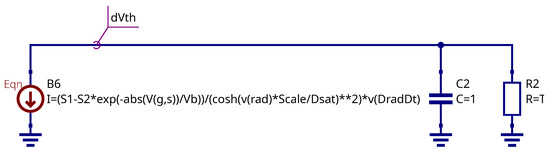
Figure 7.
The RC stage representing fading and charge accumulation.
The capacitor C2 is charged from the current source B6 which current is proportional to the time derivative of the threshold voltage shift:
The capacitor voltage is proportional to the integral of the current, and the voltage at the upper capacitor node corresponds to the threshold voltage shift. The discharge of the capacitor through the resistor R2 represents the fading effect. As the capacitor discharges, the threshold voltage shift gradually approaches zero, and the MOSFET threshold voltage returns to its pre-irradiation value.
The part of the compact model representing fading (RC circuit shown in Figure 7) is optional and may be omitted if the fading simulation is not required. Adding the fading stage adds the parameter , representing fading time constant. This additional parameter could be extracted from the threshold voltage shift fading dependency [41].
3.3. IV-Curves Simulation
The , , and are the MOSFET level 1 model parameters. Its extraction procedure is well described in the literature and not considered here. The pair of and curves are required. The used RADFET device is compatible with the CD4000 technology and these parameters could be taken from the basic technology using common SPICE model extraction methods based on IV-curve properties.
The temperature dependency parameters and are extracted from fitting of the zero temperature coefficient point at the curves family at different temperatures within the device operation range. The modeled ZTC point should match the measured ZTC point.
An example of the temperature parameters extraction is shown in Figure 8. The ZTC point for the used device achieved at the drain current A. The interception points of the IV-curves shown in the figure is located near 10 A current.
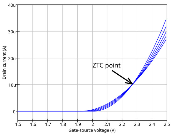
Figure 8.
Temperature dependency extraction of RADFET device.
3.4. Sensitivity Simulation
The sensitivity extraction requires the measurement of the I–V curves under different irradiation levels. We have measured the curves for three irradiation doses: 7 krad, 10 krad and 15 krad with no bias applied at gate. This data was used for sensitivity extraction. The testbench schematic in Qucs-S is shown in Figure 9. The V3 voltage source represents the absorbed dose input. The voltage at this terminal is equal to the dose in rads. Experimental results were obtained using an experimental setup implemented using a PXIe-4135 precision current/voltage generator/meter (National Instruments, Austin, TX, USA), which is a module of the PXI series from National Instruments. The setup is comprehensively described in [18].
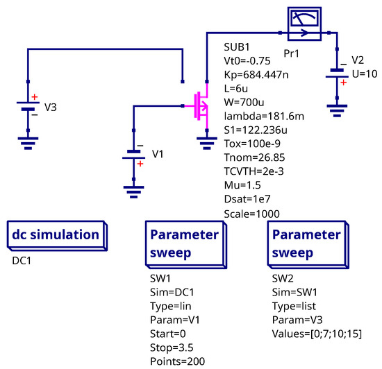
Figure 9.
Testbench schematic for I–V curves measurement.
The simulated and measured I–V curves are shown in Figure 10. The figure shows four I–V curves. The measurements were taken without radiation and under radiation levels 7 krad, 10 krad, and 15 krad. The gamma-ray 60Co source was used.
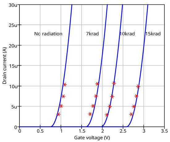
Figure 10.
Simulated (solid line) and measured (stars) I–V curves for the RADFET device.
3.5. Gate Bias Dependency of Sensitivity
The sensitivity could be extracted as the derivative of the threshold voltage:
The threshold voltage can be measured by connecting the MOSFET drain and gate to a current source while grounding the source terminal. When the source current is in the microampere range, the voltage at the drain node closely approximates the threshold voltage. The testbench schematic and the sensitivity extraction script are shown in Figure 11. Nutmeg, the scripting language of the Ngspice simulator, is used to assemble a vector representing the dependency based on the results of a single-point DC sweep simulation.
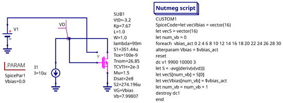
Figure 11.
Testbench schematic for sensitivity extraction.
The simulation results are presented in Figure 12. The data for the IRF9520 power MOSFET, provided in [4], were used since the gate bias dependency for the device described in Section 2.1 was not experimentally measured. The parameters , , and for this MOSFET were taken from the SPICE VDMOS model supplied by the device vendor. The simulation demonstrates good agreement with the experimental data. The extracted parameters are as follows: mV/rad, mV, and V.
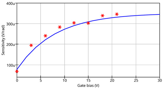
Figure 12.
Simulated (solid line) and measured (stars) sensitivity dependency on the gate bias.
3.6. Gate Current Simulation
The study presented in [22] demonstrates that utilizing gate charge injection in RADFET devices extends their range of applications. Circuit simulation enables the analysis and debugging of dosimeter circuits that operate with gate injection current. The testbench schematic for gate current simulation is shown in Figure 13. In this setup, a DC injection current source (I1) is connected to the MOSFET gate, while all other terminals are grounded. The pulsed voltage source V1 represents a virtual radiation beam, where the pulse rise time corresponds to the irradiation duration and the peak voltage represents the radiation dose D. During transient simulation, the gate voltage drop at the gate node is monitored. Both the drain and source terminals are connected to ground. The virtual current probe Pr1 is used to measure the gate current.
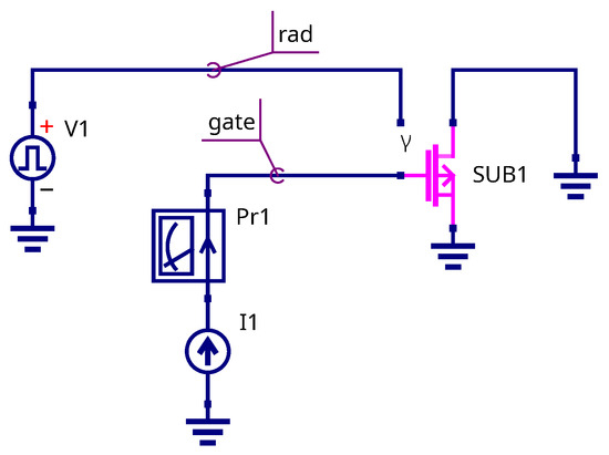
Figure 13.
Testbench schematic for the gate current simulation.
Figure 14 shows the simulation result for the testcase described in the paper [22]. The MOS sensor (RADFET) was injected by current density A/cm2. Then it was irradiated by gamma-rays to achieve the radiation current density higher than injection current density. The voltage drop on the MOS structure (RADFET) depends on the ratio of the radiation current and total current. When the radiation intensity increases, as well as the radiation current, but the voltage drops as the gate decreases. The simulation shows a good match with the data provided in [22].
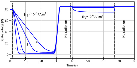
Figure 14.
Waveform of the voltage at RADFET gate under injection and irradiation for different ratio of injection and radiation currents. 1—; 2—; 3—; 4—.
4. Discussion
In the paper [18], we proposed the design of MOS radiation sensor capable of operating under conditions of high-field injection of electrons into the gate dielectric. Experimental testing of the developed sensors was carried out using gamma radiation, alpha particles and protons. The article proposed a physical model describing the physical effects occurring in the MOS sensor when exposed to ionizing radiation in a wide range of electric fields applied to the dielectric (including high-field electron injection). This article is a continuation of the research presented in [18], and in it, the previously described physical effects are taken into account in the SPICE model. As a result, it becomes possible to design RADFET sensors with specified electrophysical and metrological characteristics at the development stage. Also, depending on the modeling, it becomes possible to create more complex electronic devices for monitoring radiation, in which, along with the RADFET sensor, there are electronic components that improve the metrological characteristics and readout (telemetry) of radiation characteristics.
The designed compact model makes it possible to simulate the input stage of the dosimeter described in [43] along with its analog front end. The dosimeter input schematic is shown in Figure 15. The LM334 current source IC (REF1) provides a constant current to the drain and acts as an adjustable current source, which is commonly used in dosimeter readout circuits. The resistor R1 sets a current of 10 A, with its selection guidelines available in the IC datasheet. A SPICE macro model for the LM334 IC is supplied by the device vendor. Switches S1 and S2 are used to simulate the irradiation and measurement phases, respectively. The pulsed voltage source V1 represents a virtual radiation input, where its high voltage level U2 corresponds to the total accumulated dose. The 1 V voltage at the radiation input (wire labeled with rad) represents 1 krad dose. The rise time Tr of the pulsed source represents the duration of the irradiation phase. The delay T1, defined as the time between the start of the simulation and the beginning of the pulse, is used to improve the visual clarity of the simulation plots and can be set arbitrarily. The total pulse duration T2 should be longer than the overall simulation time. At the start of the simulation, switch S1 is closed and S2 is open. The states of the switches change at time . During irradiation, all electrodes of the RADFET are connected to ground, and the sensor operates under exposure. When the irradiation phase ends, S1 opens and S2 closes, switching the MOSFET into the measurement circuit. Under these conditions, the drain voltage corresponding to the selected drain current range is approximately equal to the MOSFET threshold voltage . The virtual current probe Pr1 is used to monitor and verify the DC operating point of the circuit.
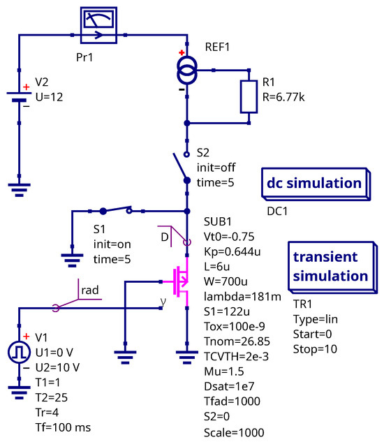
Figure 15.
The schematic of the dosimeter input designed in Qucs-S.
The simulated output voltage and input radiation dose are shown in Figure 16. During the irradiation phase, the drain voltage is equal to zero because the RADFET is disconnected from the readout circuit and its terminals are shorted. In the readout phase, the drain voltage is approximately , since the applied dose (10 krad) does not approach the saturation region and no gate bias is applied during irradiation.
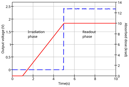
Figure 16.
The simulated output voltage of the dosimeter (dashed curve, left Y-axis) and accumulated dose (solid curve, right Y-axis).
The considered schematic shows how to use the presented RADFET compact model for the readout circuits simulation. The fading is not taken into the account. The presented approach could be extended to more complex readout circuits.
5. Conclusions
This paper presented a compact model of the RADFET device. The proposed model offers a more flexible approach compared to substituting the threshold voltage shift dependency on the accumulated dose directly into a SPICE model card parameter. The model features a dedicated input for a virtual radiation source, enabling simulation of the complex behavior of dosimeter input circuitry in response to varying radiation beam dynamics. The developed model extends standard SPICE MOSFET models and allows simulation of the following effects:
- Basic MOSFET IV-curve dependency;
- Threshold voltage shift dependency on the adsorbed does and gate bias at the irradiation phase;
- Saturation at high absorbed dose;
- Gate dielectric properties;
- Tunneling gate current and irradiation gate current;
- Threshold voltage fading after the irradiation.
A limitation of the proposed model is that the charge yield coefficient is not calculated automatically and must be manually adjusted for different types of radiation sources (for example, protons). Additionally, the bulk terminal and the threshold voltage dependency on the bulk voltage were omitted since the device’s bulk is connected to the source terminal.
The presented model is modular, allowing the fading submodule to be disabled when fading simulation is not required. The model parameters can be extracted from IV-curve measurements and threshold voltage shift measurements obtained during irradiation. The proposed model is fully compatible with the standard Level 1 SPICE MOSFET model and can be used with both open-source and proprietary SPICE simulation kernels. It is implemented in subcircuit form but can be converted to Verilog-A using a Verilog-A synthesizer. The use of the proposed compact model enables accurate simulation of dosimeter analog readout circuits, taking into account both the accumulated dose and the gate bias applied during irradiation. This capability is demonstrated through an example simulation of the dosimeter readout schematic.
Author Contributions
Conceptualization, V.A. and A.I.P.; funding acquisition, V.A.; investigation, V.K. and D.A., software, V.K.; methodology, V.K. and D.A.; supervision, V.A. and A.I.P.; visualization, S.P.; writing—original draft preparation, V.K., D.A. and S.P., writing—review and editing, V.K. and D.A. All authors have read and agreed to the published version of the manuscript.
Funding
The research was financially supported by the Ministry of Science and Higher Education of the Russian Federation as a part of the project FSFN-2024-0086.
Institutional Review Board Statement
Not applicable.
Informed Consent Statement
Not applicable.
Data Availability Statement
The source schematics and generated models are uploaded via Zenodo: https://zenodo.org/records/16936455 (accessed on 1 September 2025).
Conflicts of Interest
The authors declare no conflicts of interest.
References
- Holmes -Siedle, A.; Adams, L. RADFET: A review of the use of metal-oxide-silicon devices as integrating dosimeters. Int. J. Radiat. Appl. Instrum. Part C Radiat. Phys. Chem. 1986, 28, 235–244. [Google Scholar] [CrossRef]
- Kulhar, M.; Dhoot, K.; Pandya, A. Gamma Dose Rate Measurement Using RadFET. IEEE Trans. Nucl. Sci. 2019, 66, 2220–2228. [Google Scholar] [CrossRef]
- Camanzi, B.; Holmes-Siedle, A.G. The race for new radiation monitors. Nat. Mater. 2008, 7, 343–345. [Google Scholar] [CrossRef]
- Ristić, G.S.; Ilić, S.D.; Veljković, S.; Jevtić, A.S.; Dimitrijević, S.; Palma, A.J.; Stanković, S.; Andjelković, M.S. Commercial P-Channel Power VDMOSFET as X-ray Dosimeter. Electronics 2022, 11, 918. [Google Scholar] [CrossRef]
- Assaf, J. Characterization of Commercial P-MOSFETs for Using as a Gamma-Rays Dosimeter. Silicon 2022, 14, 1767–1774. [Google Scholar] [CrossRef]
- Pejovic, M.M. Application of p-Channel Power VDMOSFET as a High Radiation Doses Sensor. IEEE Trans. Nucl. Sci. 2015, 62, 1905–1910. [Google Scholar] [CrossRef]
- Andjelković, M.S.; Ristić, G.S.; Jakšić, A.B. Using RADFET for the real-time measurement of gamma radiation dose rate. Meas. Sci. Technol. 2015, 26, 025004. [Google Scholar] [CrossRef]
- Veljković, S.; Mitrović, N.; Davidović, V.; Golubović, S.; Djorić-Veljković, S.; Paskaleva, A.; Spassov, D.; Stanković, S.; Andjelković, M.; Prijić, Z.; et al. Response of Commercial P-Channel Power VDMOS Transistors to Ionizing Irradiation and Bias Temperature Stress. J. Circuits Syst. Comput. 2022, 31, 2240003. [Google Scholar] [CrossRef]
- Sun, Y.; Wang, T.; Liu, Z.; Xu, J. Investigation of irradiation effects and model parameter extraction for VDMOS field effect transistor exposed to gamma rays. Radiat. Phys. Chem. 2021, 185, 109478. [Google Scholar] [CrossRef]
- Ravotti, F. Dosimetry Techniques and Radiation Test Facilities for Total Ionizing Dose Testing. IEEE Trans. Nucl. Sci. 2018, 65, 1440–1464. [Google Scholar] [CrossRef]
- Siebel, O.; Pereira, J.; Souza, R.; Ramirez-Fernandez, F.; Schneider, M.; Galup-Montoro, C. A very-low-cost dosimeter based on the off-the-shelf CD4007 MOSFET array for in vivo radiotherapy applications. Radiat. Meas. 2015, 75, 53–63. [Google Scholar] [CrossRef]
- Ristić, G.S.; Vasović, N.D.; Kovačević, M.; Jakšić, A.B. The sensitivity of 100nm RADFETs with zero gate bias up to dose of 230Gy(Si). Nucl. Instrum. Methods Phys. Res. Sect. B Beam Interact. Mater. At. 2011, 269, 2703–2708. [Google Scholar] [CrossRef]
- Pejović, M.M.; Pejović, S.M. VDMOSFET as a prospective dosimeter for radiotherapy. Appl. Radiat. Isot. 2018, 132, 1–5. [Google Scholar] [CrossRef]
- Ristic, G.S.; Ilic, S.D.; Andjelkovic, M.S.; Duane, R.; Palma, A.J.; Lalena, A.M.; Krstic, M.D.; Jaksic, A.B. Sensitivity and fading of irradiated RADFETs with different gate voltages. Nucl. Instrum. Methods Phys. Res. Sect. A Accel. Spectrometers Detect. Assoc. Equip. 2022, 1029, 166473. [Google Scholar] [CrossRef]
- Schwank, J.R.; Shaneyfelt, M.R.; Fleetwood, D.M.; Felix, J.A.; Dodd, P.E.; Paillet, P.; Ferlet-Cavrois, V. Radiation Effects in MOS Oxides. IEEE Trans. Nucl. Sci. 2008, 55, 1833–1853. [Google Scholar] [CrossRef]
- Oldham, T.; McLean, F. Total ionizing dose effects in MOS oxides and devices. IEEE Trans. Nucl. Sci. 2003, 50, 483–499. [Google Scholar] [CrossRef]
- Lipovetzky, J.; Holmes Siedle, A.; Garcia Inza, M.; Carbonetto, S.; Redin, E.; Faigon, A. New Fowler-Nordheim Injection, Charge Neutralization, and Gamma Tests on the REM RFT300 RADFET Dosimeter. IEEE Trans. Nucl. Sci. 2012, 59, 3133–3140. [Google Scholar] [CrossRef]
- Andreev, D.V.; Andreev, V.V.; Konuhova, M.; Popov, A.I. Technique of High-Field Electron Injection for Wafer-Level Testing of Gate Dielectrics of MIS Devices. Technologies 2024, 12, 102. [Google Scholar] [CrossRef]
- Peng, L.; Hu, D.; Jia, Y.; Wu, Y.; An, P.; Jia, G. Analysis on the Rapid Recovery of Irradiated VDMOSFETs by the Positive High Electric Field Stress. IEEE Trans. Nucl. Sci. 2017, 64, 2633–2638. [Google Scholar] [CrossRef]
- Andreev, D.V.; Bondarenko, G.G.; Andreev, V.V. Change in the Charge State of MOS Structures with a Radiation-Induced Charge under High-Field Injection of Electrons. J. Surf. Investig. X-Ray Synchrotron Neutron Tech. 2023, 17, 48–53. [Google Scholar] [CrossRef]
- Andreev, D.V.; Bondarenko, G.G.; Andreev, V.V.; Stolyarov, A.A. Use of High-Field Electron Injection into Dielectrics to Enhance Functional Capabilities of Radiation MOS Sensors. Sensors 2020, 20, 2382. [Google Scholar] [CrossRef] [PubMed]
- Andreev, V.V.; Bondarenko, G.G.; Andreev, D.V.; Stolyarov, A.A. Use of MIS Sensors of Radiation in High-Field Electron Injection Modes. J. Contemp. Phys. (Armenian Acad. Sci.) 2020, 55, 144–150. [Google Scholar] [CrossRef]
- Andreev, V.V.; Maslovsky, V.M.; Andreev, D.V.; Stolyarov, A.A. Charge effects in dielectric films of MIS structures being under high-field injection of electrons at ionizing radiation. In Proceedings of the International Conference on Micro- and Nano-Electronics 2018, Zvenigorod, Russia, 1–5 October 2018; Lukichev, V.F., Rudenko, K.V., Eds.; International Society for Optics and Photonics (SPIE): Bellingham, WA, USA, 2019; Volume 11022, p. 1102207. [Google Scholar] [CrossRef]
- Mitrović, N.; Guirado, D.; Danković, D.; Palma, A.J.; Ristić, G.; Carvajal, M.A. Thermal Annealing-Induced Recovery of the VT of Irradiated Commercial MOS Transistors. J. Circuits Syst. Comput. 2025, 34, 2541002. [Google Scholar] [CrossRef]
- Vladirmirescu, A. Shaping the History of SPICE. IEEE Solid-State Circuits Mag. 2011, 3, 36–39. [Google Scholar] [CrossRef]
- De Graaff, H.C.; Kloosterman, W.J.; Versleyen, M. Compact Modelling for Analoge Circuit Design. In Proceedings of the ESPRIT ’90, Brussels, Belgium, 12–15 November 1990; pp. 65–76. [Google Scholar]
- Oh, J.H.; Yu, Y.S. Macro-Modeling for N-Type Feedback Field-Effect Transistor for Circuit Simulation. Micromachines 2021, 12, 1174. [Google Scholar] [CrossRef]
- Ji, S.; Mappes, J.; Koudelka, P.; Scardelletti, M.C.; Zorman, C.; Lavasani, H.M. An Enhanced Verilog-A Model for Graphene Field-Effect Transistors Using Variable Fermi Velocity. Electronics 2024, 13, 5051. [Google Scholar] [CrossRef]
- Kasprowicz, D. Table-Based Model of a Dual-Gate Transistor for Statistical Circuit Simulation. IEEE Trans. Comput.-Aided Des. Integr. Circuits Syst. 2019, 38, 1493–1500. [Google Scholar] [CrossRef]
- Kuznetsov, V. Microstrip Line Modeling Taking into Account Dispersion Using a General-Purpose SPICE Simulator. J. Low Power Electron. Appl. 2025, 15, 42. [Google Scholar] [CrossRef]
- Marjanović, M.; Ilić, S.D.; Veljković, S.; Mitrović, N.; Gurer, U.; Yilmaz, O.; Kahraman, A.; Aktag, A.; Karacali, H.; Budak, E.; et al. The SPICE Modeling of a Radiation Sensor Based on a MOSFET with a Dielectric HfO2/SiO2 Double-Layer. Sensors 2025, 25, 546. [Google Scholar] [CrossRef]
- Mrozovskaya, E.; Zimin, P.; Chubunov, P.; Zebrev, G. Compact modeling of electrical characteristics of p-MNOS based RADFETs. In Proceedings of the International Conference on Micro- and Nano-Electronics 2018, Zvenigorod, Russia, 1–5 October 2018; Lukichev, V.F., Rudenko, K.V., Eds.; International Society for Optics and Photonics (SPIE): Bellingham, WA, USA, 2019; Volume 11022, p. 110220I. [Google Scholar] [CrossRef]
- Meguellati, M.; Djeffal, F. New Dual-Dielectric Gate All Around (DDGAA) RADFET dosimeter design to improve the radiation sensitivity. Nucl. Instrum. Methods Phys. Res. Sect. A Accel. Spectrometers Detect. Assoc. Equip. 2012, 683, 24–28. [Google Scholar] [CrossRef]
- Andreev, D.V.; Maslovsky, V.M.; Andreev, V.V.; Stolyarov, A.A. Modified Ramped Current Stress Technique for Monitoring Thin Dielectrics Reliability and Charge Degradation. Phys. Status Solidi A 2022, 219, 2100400. [Google Scholar] [CrossRef]
- Fleetwood, D.M. Perspective on radiation effects in nanoscale metal–oxide–semiconductor devices. Appl. Phys. Lett. 2022, 121, 070503. [Google Scholar] [CrossRef]
- Brinson, M.; Kuznetsov, V. Qucs-0.0.19S: A new open-source circuit simulator and its application for hardware design. In Proceedings of the 2016 International Siberian Conference on Control and Communications (SIBCON), Moscow, Russia, 12–14 May 2016; pp. 1–5. [Google Scholar] [CrossRef]
- Grabinski, W.; Scholz, R.; Verley, J.; Keiter, E.R.; Vogt, H.; Warning, D.; Nenzi, P.; Lannutti, F.; Salfelder, F.; Davis, A.; et al. FOSS CAD for the Compact Verilog-A Model Standardization in Open Access PDKs. In Proceedings of the 2024 8th IEEE Electron Devices Technology & Manufacturing Conference (EDTM), Bangalore, India, 3–6 March 2024; pp. 1–3. [Google Scholar] [CrossRef]
- Lannutti, F.; Nenzi, P.; Olivieri, M. KLU sparse direct linear solver implementation into NGSPICE. In Proceedings of the 19th International Conference Mixed Design of Integrated Circuits and Systems—MIXDES 2012, Warsaw, Poland, 24–26 May 2012; pp. 69–73. [Google Scholar]
- Kuthe, P.; Müller, M.; Schröter, M. VerilogAE: An Open Source Verilog-A Compiler for Compact Model Parameter Extraction. IEEE J. Electron Devices Soc. 2020, 8, 1416–1423. [Google Scholar] [CrossRef]
- Chauhan, Y.S.; Venugopalan, S.; Paydavosi, N.; Kushwaha, P.; Jandhyala, S.; Duarte, J.P.; Agnihotri, S.; Yadav, C.; Agarwal, H.; Niknejad, A.; et al. BSIM compact MOSFET models for SPICE simulation. In Proceedings of the 20th International Conference Mixed Design of Integrated Circuits and Systems—MIXDES 2013, Gdynia, Poland, 20–22 June 2013; pp. 23–28. [Google Scholar]
- Ristic, G.S.; Ilic, S.D.; Duane, R.; Andjelkovic, M.S.; Palma, A.J.; Lallena, A.M.; Krstic, M.D.; Stankovic, S.J.; Jaksic, A.B. Radiation sensitive MOSFETs irradiated with various positive gate biases. J. Radiat. Res. Appl. Sci. 2021, 14, 353–357. [Google Scholar] [CrossRef]
- Pejović, M.M. Dose response, radiation sensitivity and signal fading of p-channel MOSFETs (RADFETs) irradiated up to 50Gy with 60Co. Appl. Radiat. Isot. 2015, 104, 100–105. [Google Scholar] [CrossRef]
- Vasović, N.D.; Ristić, G.S. A new microcontroller-based RADFET dosimeter reader. Radiat. Meas. 2012, 47, 272–276. [Google Scholar] [CrossRef]


Disclaimer/Publisher’s Note: The statements, opinions and data contained in all publications are solely those of the individual author(s) and contributor(s) and not of MDPI and/or the editor(s). MDPI and/or the editor(s) disclaim responsibility for any injury to people or property resulting from any ideas, methods, instructions or products referred to in the content. |
© 2025 by the authors. Licensee MDPI, Basel, Switzerland. This article is an open access article distributed under the terms and conditions of the Creative Commons Attribution (CC BY) license (https://creativecommons.org/licenses/by/4.0/).