Article

Mitigation and Predictive Assessment of SET Immunity of Digital Logic Circuits for Space Missions

1
Institut d’Electronique et des Systèmes, Université de Montpellier, 5214, 860 Rue de St Priest, Bat. 5, F-34097 Montpellier, France
2
Institut Materiaux Microelectronique Nanoscience de Provence, Aix-Marseille Université, 13013 Marseille, France
3
Advanced Integrated Sensing Lab, KU Leuven University, 2440 Geel, Belgium
*
Author to whom correspondence should be addressed.
Aerospace 2020, 7(2), 12; https://doi.org/10.3390/aerospace7020012
Submission received: 20 December 2019 / Revised: 24 January 2020 / Accepted: 3 February 2020 / Published: 5 February 2020
(This article belongs to the Special Issue Single Event Effect Prediction in Avionics)

Abstract

:
Due to the intrinsic masking effects of combinational circuits in digital designs, Single-Event Transient (SET) effects were considered irrelevant compared to the data rupture caused by Single-Event Upset (SEU) effects. However, the importance of considering SET in Very-Large-System-Integration (VLSI) circuits increases given the reduction of the transistor dimensions and the logic data path depth in advanced technology nodes. Accordingly, the threat of SET in electronics systems for space applications must be carefully addressed along with the SEU characterization. In this work, a systematic prediction methodology to assess and improve the SET immunity of digital circuits is presented. Further, the applicability to full-custom and cell-based design methodologies are discussed, and an analysis based on signal probability and pin assignment is proposed to achieve a more application-efficient SET-aware optimization of synthesized circuits. For instance, a SET-aware pin assignment can provide a reduction of 37% and 16% on the SET rate of a NOR gate for a Geostationary Orbit (GEO) and the International Space Station (ISS) orbit, respectively.

1. Introduction

Within the advancements of technology process, an increased susceptibility to radiation effects is observed in deeply scaled Complementary Metal-Oxide Semiconductor (CMOS) transistors [1]. Energetic particles present in harsh environments, such as in space or in the Earth’s atmosphere, can induce physical and functional damage to electronics systems in space missions. Single-Event Effects (SEEs) are a group of destructive and nondestructive effects originating from a single particle hit in electronic devices. When a single particle hits a memory element, such as a Static Random-Access Memory (SRAM) or flip-flops, and it changes the stored bit value, a so-called Single-Event Upset (SEU) occurs. Similarly, if the particle hits a combinational logic circuitry, a parasitic transient is observed in the circuit node characterizing a Single-Event Transient (SET). Historically, SEUs have been vastly studied in the literature while SETs were not given important attention due to the intrinsic masking effects of combinational logic circuits [2]. There are three main masking effects inherent in digital circuits: (i) Electrical masking, in which the transient pulse is not able to propagate through a logic path due to electrical losses and attenuation of its amplitude; (ii) logical masking, in which a SET will be masked due to the logic dependence of each digital signal; and, (iii) latch-window masking or temporal masking, in which the SET pulse is masked by the latching window of a memory element, i.e., the SET does not reach the memory element on its writing mode. However, the transistor scaling, the reduced logic data path depth, and the increased operating frequencies have attenuated the electrical, logical, and latch-window masking effects of logic circuits at advanced technology nodes [3,4,5,6].
The use of modeling and simulation has always been present in the study of physical phenomena, especially in the field of electronics to study the behavior of MOS transistors [7,8]. Further, with the increase of complexity of very-large-scale-integration (VLSI) system, it is increasingly necessary to use the support of simulation studies to verify and assist the development of such circuits. In this sense, Monte Carlo simulation tools have solid foundations to be used in the study of radiation effects on electronics [9]. There are many works in the literature which propose the research of radiation effects on electronics exploiting simulations and avoiding the time consuming and expensive radiation campaigns [10,11,12,13,14,15,16,17]. Mixed-mode Technology Computer-Aided Design (TCAD) simulations have been vastly used to understand the main mechanisms in SEEs on electronics. However, Monte Carlo simulation codes have a computation time several orders of magnitude lower than mixed-mode TCAD simulations [9,16]. Accordingly, a diverse number of modeling based on Monte Carlo simulations have been proposed to estimate and predict the radiation robustness of electronics [10,11,12,13,14,15,16]. In this work, a layout-based prediction methodology using the MC-Oracle tool is presented. Additionally, the paper discusses the applicability of the proposed SET characterization on acquiring a SET-aware circuit design methodology. Additionally, to conclude, mitigation schemes based on signal probability and pin assignment optimization is proposed and evaluated.
The paper is organized as follows. The prediction methodology and its applicability to address reliability-aware logic synthesis in standard-cell based design are discussed in Section 2. Section 3 presents the results and discussion of: The SET immunity assessment of a set of standard cells; the impact of low-power design techniques; and, a new hardening strategy based on a SET-aware pin assignment. To conclude, Section 4 summarizes the paper and presents some conclusions.

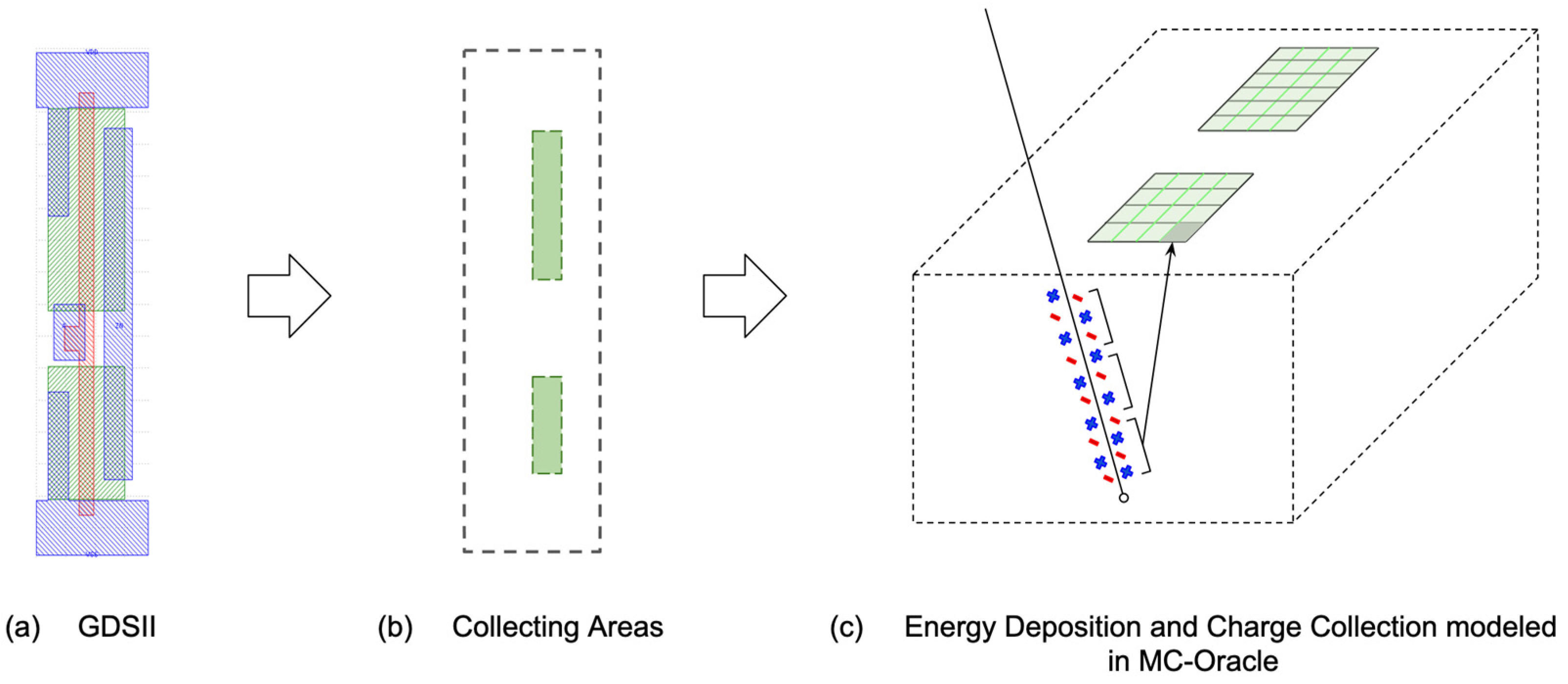
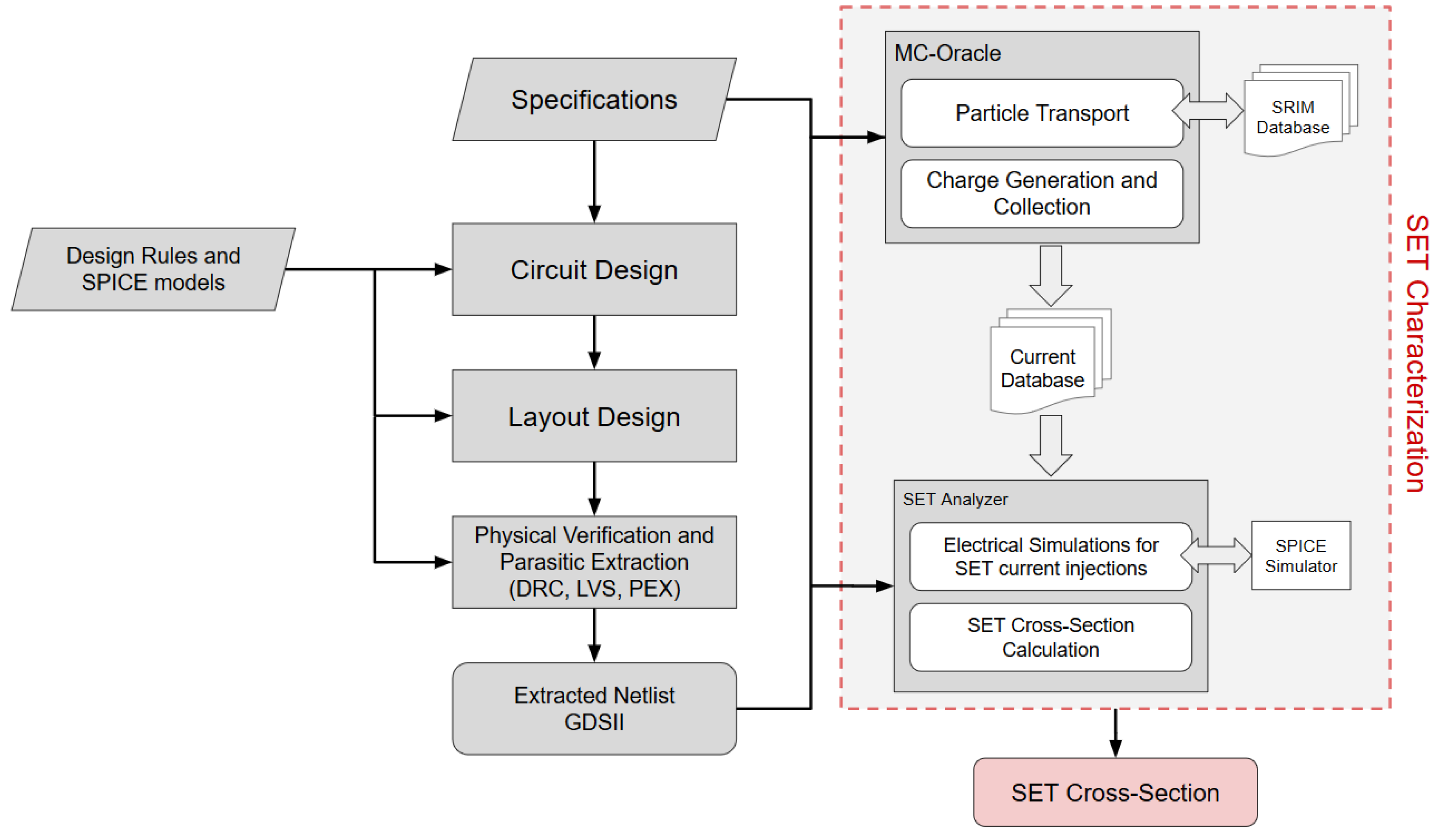
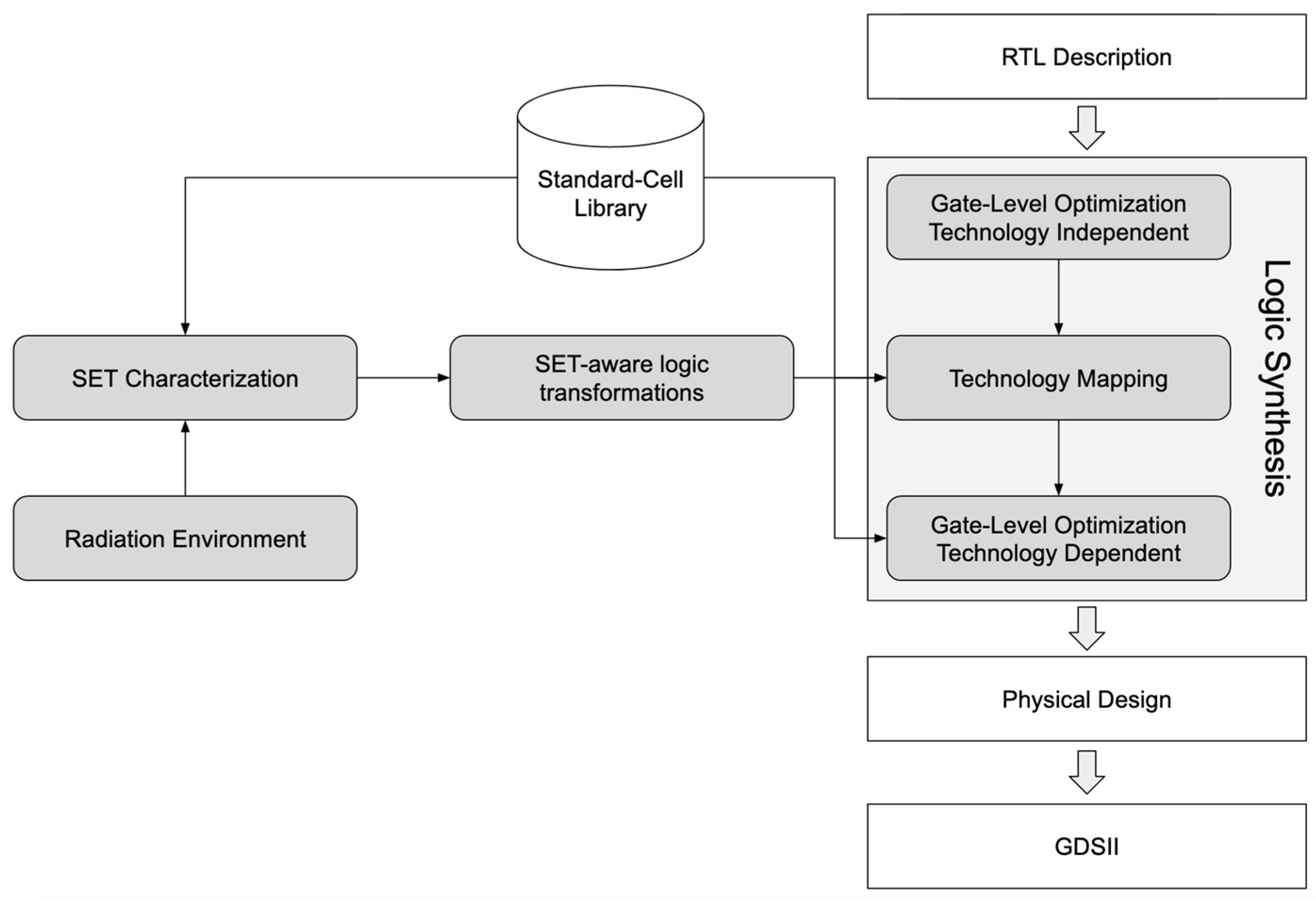
2. Prediction Methodology Based on the Mc-Oracle Tool

To accurately assess the SEE immunity of digital circuits, it is highly recommended to adopt a multi-scale and multi-physics methodology due to the plurality of complex effects involved at the silicon and circuit level [10,11]. Different approaches taking into consideration the aspects from the particle interaction physics to the circuit layout design is explored in different codes as shown in [16]. Additionally, due to the technology scaling, emerging effects as Parasitic Bipolar Amplification (PBA) and charge sharing effects need to be carefully addressed [13,18]. Therefore, layout information from the circuit design is an important determinant on the SEE prediction of electronic circuits. This work presents a layout-based methodology to assess the SEU/SET robustness of digital circuits using the MC-Oracle prediction tool [12].
MC-Oracle is a Monte Carlo simulation code developed to analyze the SEU/SET immunity of electronics based on the particle interaction physics within the sensitive devices. As neutrons, protons and ions can be simulated, the SEU/SET sensitivity can be calculated for different radiation environments such as space, atmosphere, ground, and accelerators. The energetic particles when interacting with silicon material go through the ionization process (i.e., generation of electron-hole pairs), in which parasitic charge is deposited and can be collected by the sensitive transistor junctions. Since neutrons are uncharged particles, they do not experience coulomb’s interactions with orbital electrons. Consequently, neutrons cannot ionize matter directly, however it is still considered as a threat for electronics in space [19,20]. Considering neutrons can experience nuclear reactions with the material target nuclei, they can induce SEE through indirect ionization, i.e., the ionization of secondary products of nuclear reactions. Moreover, as it presents no electromagnetic interaction, neutrons are highly penetrating particles. In the MC-Oracle, the ionization process is modeled using tables of range and electronics stopping power pre-calculated with the Stopping and Range of Ions in Matter (SRIM) code [21,22]. For the nuclear reactions induced by protons or neutrons, a precalculated nuclear database for a given energy range is built based on the Detailed History Of Recoiling Ions induced by Nucleons (DHORIN) code [23]. The location of each nuclear reaction is determined considering the information from the nuclear database in which the mean free path of each particle, i.e., the average distance travelled between collisions, is estimated from the nuclear cross-section.
Once the energy deposition is modeled by ionization and nuclear reactions, the charge transport and collection are modeled by the drift-diffusion mechanism. Drift is a mechanism governed by the electric field present in the p-n junction of the sensitive devices. For instance, when a particle hits directly the sensitive collecting area of the circuit, the carriers will be rapidly collected due to the high electric field present in the reverse-biased p-n junctions. On the other hand, diffusion is a carrier transport mechanism governed by the carrier concentration gradients. It means that the carriers will transport from regions with high to low concentration. Accordingly, in the MC-Oracle, hundreds of thousands of particles interactions are simulated and the resulting ionizing electron-hole path is numerically divided into small fragments and the transport of the carriers is calculated [12,24]. A simplified representation of the layout-based analysis using MC-Oracle is shown in Figure 1. Given a GDSII (Graphical Design System) file of the circuit, the collecting drain area of transistors can be identified and extracted to be submitted as input to the MC-Oracle calculations. In this example, the layout design of an inverter logic gate is shown in Figure 1a. The drain area of the p-type (PMOS) and n-type (NMOS) devices are extracted as shown in Figure 1b. Then, considering a heavy-ion simulation (Figure 1c), the resulting ionizing track is numerically divided into small fragments in which the generated charges diffuse to the collecting drain areas. Each collecting area is divided into elementary collecting areas and the induced transient current is calculated from the integration of the collected charge along the ionizing track for each elemental section of the collecting area (Figure 1c) [18,24].
In summary, the transient current ID of each collecting drain node is obtained following Equation (1) [18,24]:
I D ( t ) = q . v   L E T ( l )   e r 2 4 D t ( 4 π D t ) 3 2   d x d y d l
where q is the elementary charge, v is the carrier velocity in the junction, LET(l) is the ion Linear Energy Transfer (LET) along the ion track, r is the distance between the elemental section of the collecting area and the ion track, and D is the ambipolar diffusion coefficient. For each particle event, MC-Oracle calculates the induced transient current for each collecting area of the circuit design and stores this information in a SET current database. Therefore, multiple-node charge collection effects such as charge sharing mechanism and pulse quenching effects can be evaluated using this tool [18]. A simplified full custom design flow with the SET characterization methodology using MC-Oracle is shown in Figure 2. Given the specifications concerning the system functionality and reliability (including the radiation environment), the design engineer can start the circuit design process. Once the physical verification, i.e., Design Rule Check (DRC), Layout versus Schematic (LVS) are performed, the parasitic extraction of the netlist description and GSDII file can be obtained and submitted to the SET characterization.
The proposed SET characterization is divided into two steps: First, aiming to build an SET current database, the MC-Oracle is used to perform the particle transport and charge collection in the collecting areas of the circuit; second, an SET analyzer is responsible for the SPICE (Simulation Program with Integrated Circuit Emphasis) injection campaign using the current database provided by MC-Oracle. The main inputs to the SET characterization are: Technology model, radiation environment specification, layout design (GSDII), and extracted netlist description of the circuit. For the SET cross-section calculation and the pulse width measurement, the SET analyzer only considers the transient pulses with peak voltage higher than half of the supply voltage, but it can be easily adjusted to the needs of the user. According to the input signals of the analyzed circuit, a customized multiple-node transient injection is performed to provide an input dependence analysis of the SET sensitivity. For all SPICE simulations, a minimum-sized inverter gate is coupled to the output signal of the analyzed circuits, i.e., all circuits have a Fan-Out 1 (FO1). However, the variation of the fan-out of the circuits can also be studied by changing the circuit coupled in the output. For each particle LET, thousands of particles are simulated to reach the minimum of 100 observed events. Since the confidence is the root square of the number of events, with a minimum of 100 events, 10% of confidence is obtained. Different hardening techniques can be adopted to prevent the critical electronics systems, such as spacecrafts and aviation control systems, that fail due to the occurrence of SEEs. Accordingly, the proposed predictive SET characterization methodology allows the investigation of the hardening effectiveness of Radiation-Hardening-By-Design (RHBD) techniques at the layout level.
The development of electronic circuits for space and aviation can be done using different circuit design methodologies, from Field Programmable Gate-Arrays (FPGAs) to full-custom or cell-based Application Specific Integrated Circuits (ASICs). FPGA-based designs provide fast prototyping in the cost of area and performance when compared to full-custom designs [25,26]. However, the use of ASICs provides the best tradeoff between performance, power consumption, and circuit area. One of the main design methodologies adopted in ASICs is the standard-cell methodology in which thousands of predesigned and characterized logic gates, so called “standard-cell logic gates”, are used to design complex VLSI circuits. A considerable effort has been given to adopt mitigation strategies early in the design flow of a VLSI circuit [27,28,29,30]. The proposed predictive SET characterization methodology (Figure 2) can be integrated into the logic synthesis of a cell-based circuit design as shown in Figure 3. From an RTL (Register Transfer Level) description, the logic synthesis is able to translate function to a netlist description of logic gates using a given Standard-Cell library. It can be divided into three main processes [31]: The gate-level optimization independent of technology, i.e., the Boolean equations described in the RTL are optimized to minimize its size and the number of literals; the technology mapping, in which each logic function is transformed into a logic gate (NAND, NOR, AND, OR, and etc.) from the given cell library; the gate-level optimization technology dependent, in which optimizations on the gate netlist will be performed to minimize delay in critical paths, power consumption, and area usage. The gate netlist consists of a logic level representation of the circuit containing gate instances, from the standard-cell library, and its corresponding port connectivity. Thus, the logic synthesis has a major impact on the resulting gate netlist and therefore on the SEE immunity of the final circuit design. In the technology mapping, the technology-independent circuit is decomposed into basic primitive logic cells (Inverter NAND, or NOR gates). After the decomposition, a pattern matching process is performed to identify structural and functional patterns to be used in the covering process, which the best patterns will be implemented following a cost function, i.e., delay, area, and power consumption. Therefore, by assessing the SET immunity of basic logic cells and combinations of cells, it is possible to develop a reliability-driven cost function in the technology mapping. In a previous work, the proposed SET characterization methodology (Figure 2) was used to study the impact of adopting complex-logic standard cells compared to its counterpart implementation based on primitive logic cells [32]. Results have shown a higher SET cross-section for the complex-logic cells due to the suppression of the logic masking effects inherently present in its counterpart implementation [32].
In the physical design process, the synthesized gate netlist provided by the logic synthesis is converted into the geometric representations of different layers used in the manufacturing process, so called circuit layout. It is also in this step in which each logic cell layout is placed and its connections routed to minimize wirelength and improve power/performance metrics. However, the work in [27] proposed a cell placement to improve the induced SER of the circuit, instead. The placement algorithm focused on reducing the charge sharing effects. Similarly, by utilizing the SET characterization methodology on a cell library, a set of SET-aware logic transformations can be derived and adopted into the logic synthesis to improve the SET immunity of the final synthesized gate netlist.
In the next section, this methodology is used to assess the SET immunity of standard-cell logic gates from the 45 nm NanGate library. Additionally, the impact of adopting low-power techniques such as multiple VTH devices and dynamic voltage scaling is also explored. To conclude, SET mitigation based on the assessment provided by the proposed predictive SET characterization methodology into the circuit design flow is explored with signal probability and pin assignment optimization.

3. Results and Discussions

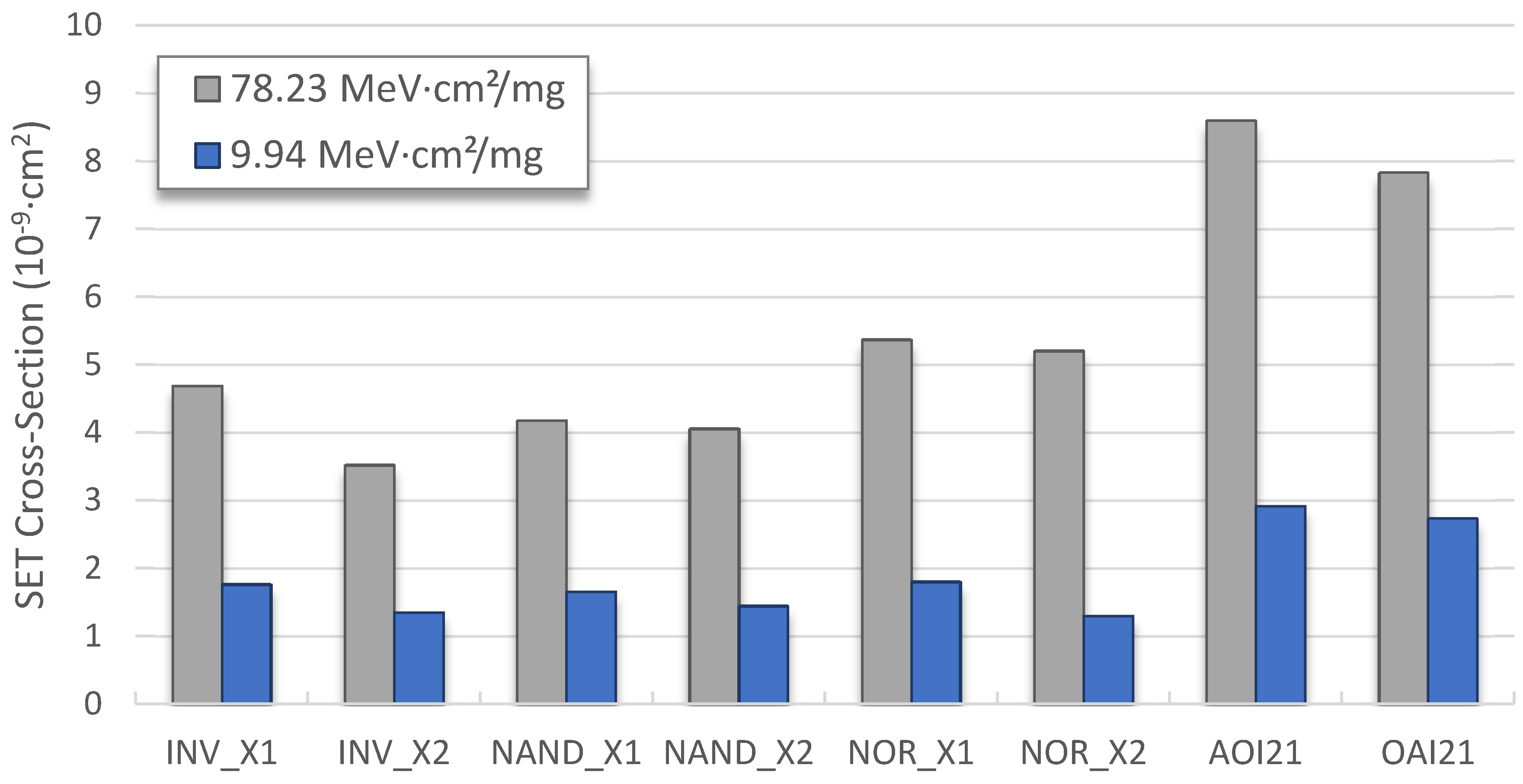
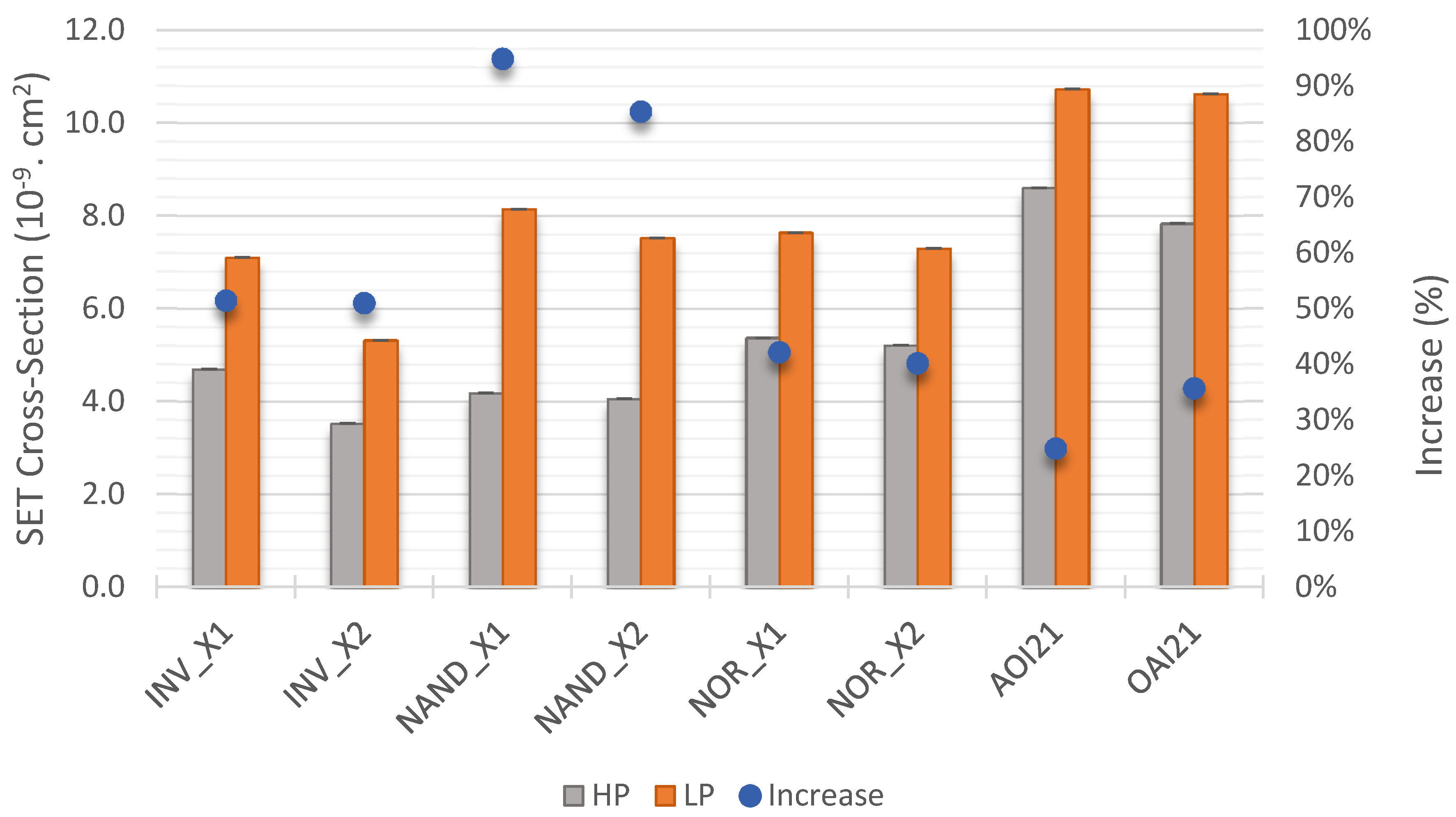
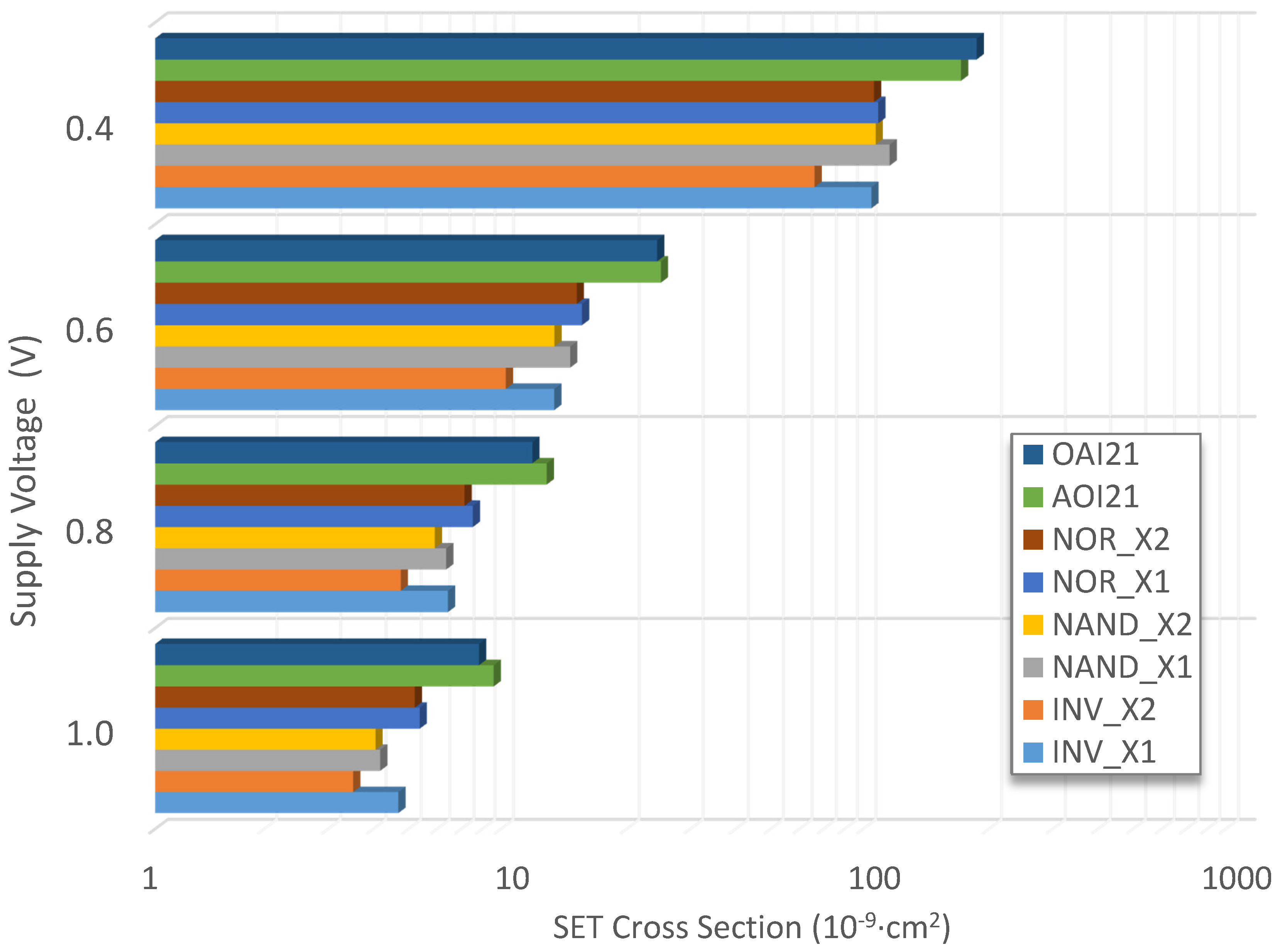
3.1. SET Immunity of Standard-Cell Logic Gates

In this work, a cell level analysis is provided with eight standard-cell gates from the 45 nm NanGate library [33]. However, the methodology is also suitable to evaluate the electrical, logical, and latch-window masking effects at logic data paths composed of a combination of single-cell gates. The eight standard cells were characterized under heavy ions and the SET cross-section is shown in Figure 4. Two different drive strengths were selected for the inverter, NAND, and NOR gates. For both LET values, the circuits with higher drive strength (X2) have shown lower cross-section, as expected [34]. A common hardening technique is to upsize transistor dimensions to increase the nodal capacitance of the circuit and, consequently, the critical charge needed to observe a SET [34,35,36,37]. For 78 MeV·cm2/mg, the INV_X2, NAND_X1, and NAND_X2 provide the lowest SET cross-sections from all analyzed cells. The And-Or-Inverter (AOI) and the Or-And-Inverter (OAI) gates implement a larger logic function, therefore, a larger layout area is used to design the circuits. Consequently, a higher SET cross-section is observed when compared with the primitive logic cells. Based on this information, a SET-aware technology mapping could be adopted by associating a reliability cost to each logic gate. The weight or cost of each gate can be calculated based on the radiation requirements of the mission and the SET cross-section or in-orbit SET rate estimated with the methodology proposed in Figure 2.
One of the primary goals of logic synthesis is to minimize the delay in critical paths. This is achieved by choosing the cells with a lower propagation time, and it can be done by adopting multiple threshold voltage VTH circuits [38]. Devices with a low VTH provide a faster switching time and consequently speed up the circuit. However, an increase in the static power consumption is observed due to the increase in leakage currents. On the other hand, the use of high-VTH devices reduces the leakage currents in the cost of performance degradation. Accordingly, multiple VTH cells are widely used to optimize the gate netlist regarding the delay and power consumption [39]. This multiple-VTH assignment can also be addressed using the proposed SET characterization methodology. In Figure 5, the standard cells were characterized using a High-Performance (HP) process technology, i.e., low-VTH devices, and a Low-Power (LP) process technology, i.e., high-VTH devices. Overall, an increased cross-section for the circuits based on the LP technology is noticed. This behavior is in agreement with the literature, in which it was shown that the increase on the threshold voltage leads to degradation of driving strength capability [40,41,42]. The NAND gates are the most sensitive to this VTH variation with a cross-section increase of 95% and 85% for the NAND_X1 and NAND_X2, respectively. In addition to its higher cross-section, the lowest increase was obtained for the complex-logic gates AOI21 and OAI21.
Another widely used technique in low-power systems is the adoption of dynamic voltage scaling [43]. However, reducing the supply voltage of the circuits increases the delay and the sensitivity to radiation effects [44,45]. In the SET analyzer (Figure 2), the circuit designer can evaluate the impact of adopting the dynamic voltage scaling on the SET immunity of the logic gates. In Figure 6, the SET cross-section of each gate is estimated considering the supply voltage scaling from 1 to 0.4 V (near-threshold regime). Reducing the supply voltage directly reduces the critical charge necessary to observe a SEE in the circuit output [44]. In a nominal supply voltage scenario, the NAND gates are preferable than NOR gates as they provide a lower SET cross-section. However, when considering a supply voltage scaling to 0.4 V, the NOR gates have shown a lower cross-section instead. This difference is attributed to the different drive capability impact on the transistor networks present on each gate design. Accordingly, in a system design focused on low-power design dynamic supply voltage, logic synthesis should consider a higher usage of NOR gates instead of NAND gates.

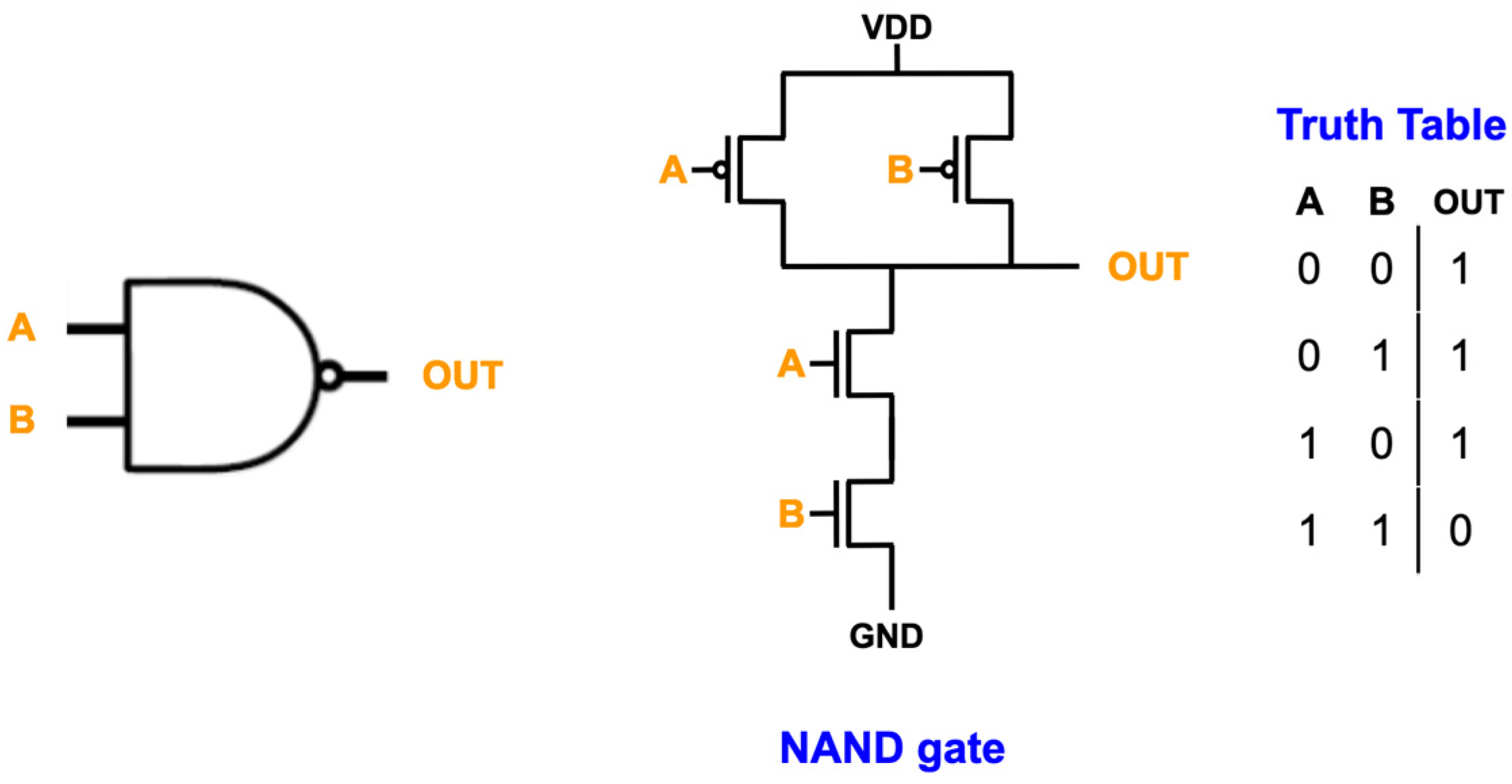
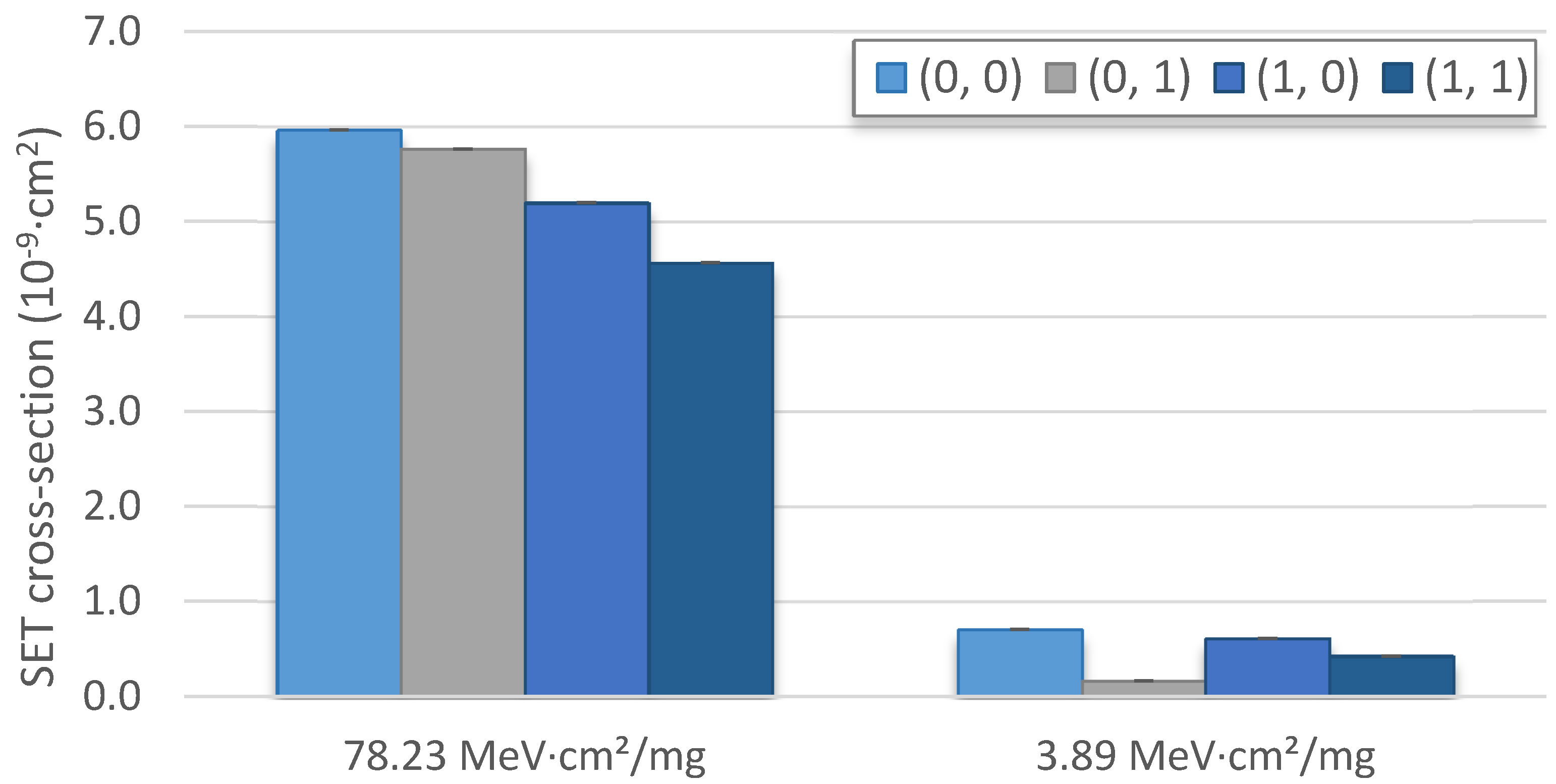
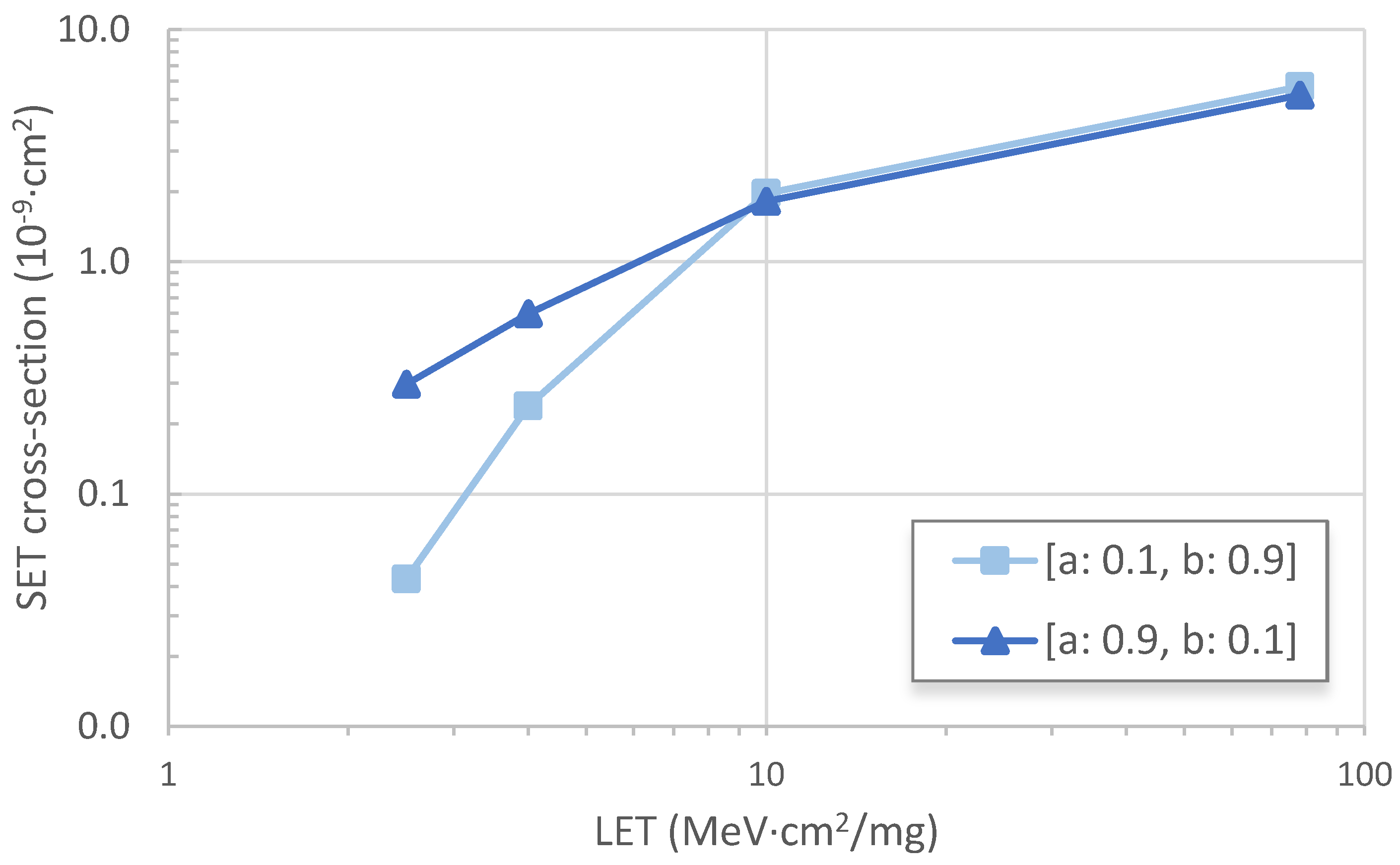
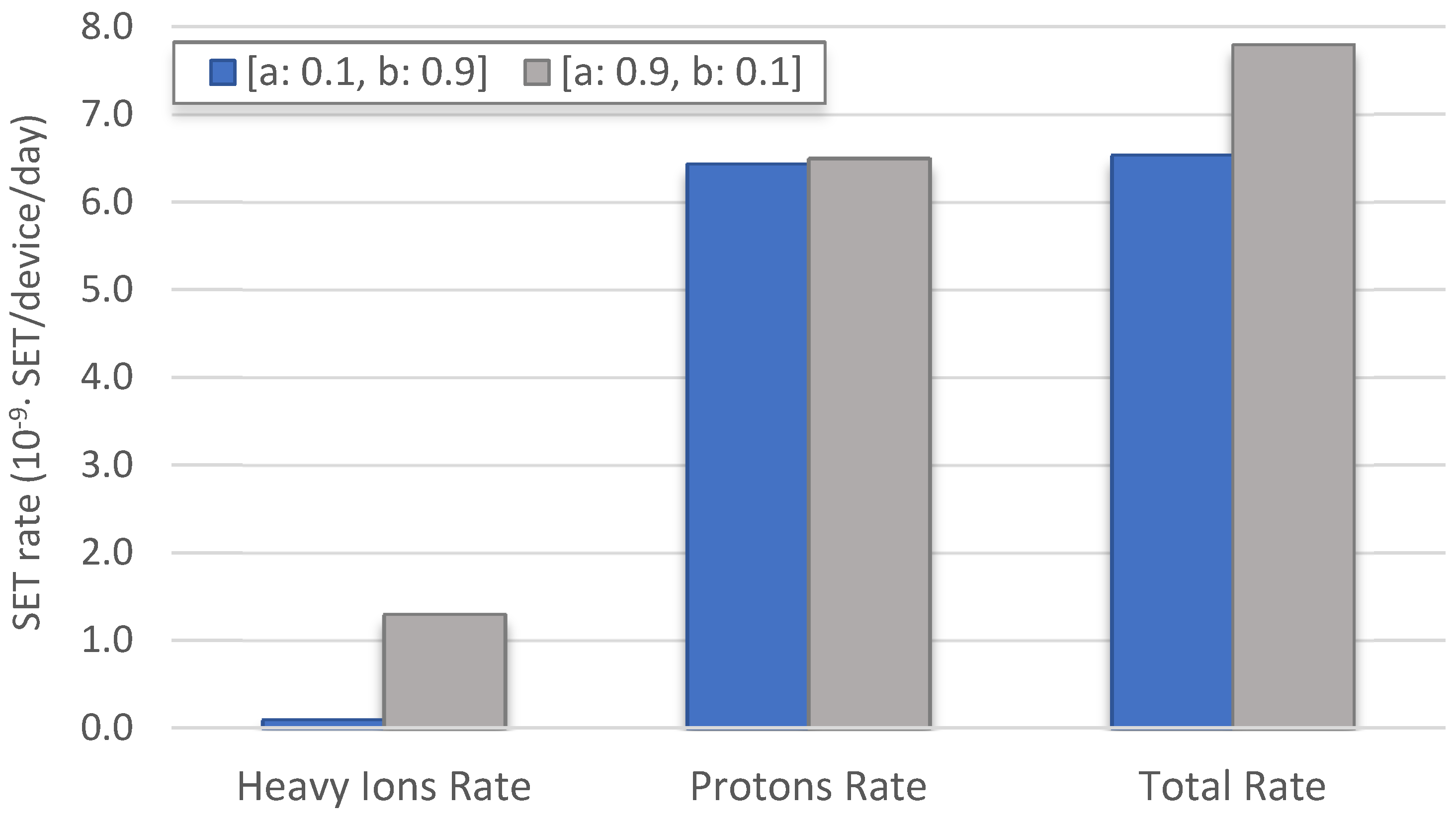
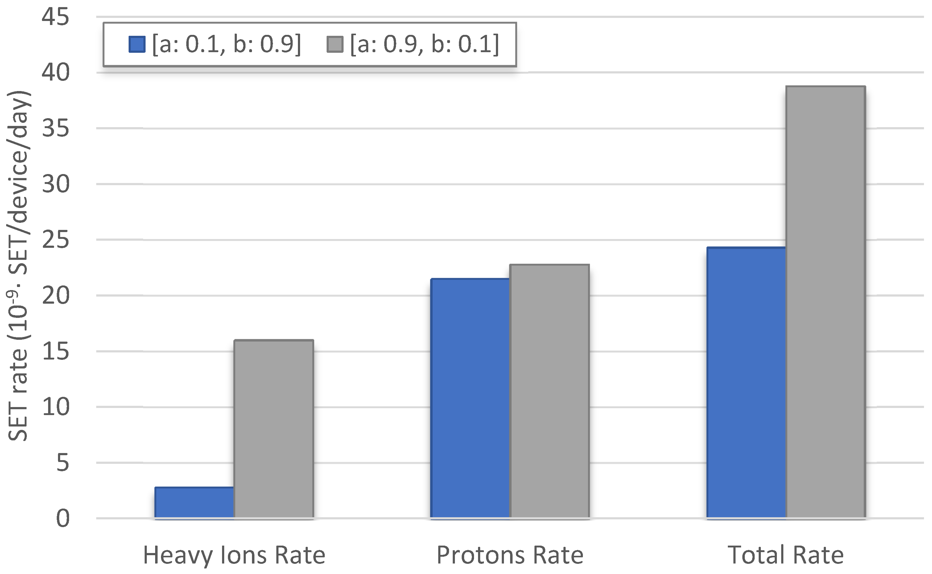
3.2. Impact of Signal Probability and Input Dependence

The SET characterization of logic gates presents an input dependence due to the different interplay relation of sensitive collecting drain areas and restoring current as shown in [32,35]. The signal switching activity is used to estimate power consumption in the design process of VLSI circuits, but it can also be used to support reliability analysis as shown in [46,47,48]. Until now, the SET cross-section calculation on this work has considered the arithmetic mean between the cross-section obtained for each input signal combination separately, i.e., the same probability to each input combination is considered. However, the proposed predictive SET characterization (Figure 2) can also consider the signal probability information of a given system application in order to estimate a more realistic cross-section. Moreover, by considering signal probabilities, it is possible to propose more application-efficient mitigation transformations on the circuit synthesis (Figure 3).
Consider the cross-section calculated for each input combination of the NAND2_X1 for heavy ion with LET = 78.23 MeV·cm2/mg, shown in Table 1. The gate-level and the transistor network representation of the NAND2_X1 is shown in Figure 7 along with its truth table. The most sensitive input combination is the (1, 1), with a cross-section of 6.75 × 10⁻⁹ cm2, when both PMOS transistors are in off-state, while the most robust is the vector (0, 0). Table 1 provides three scenarios of signal probability and the following notation is adopted: [a:p(a = 1), b:p(b = 1)], in which p(a = 1) and p(b = 1) are the probability of input a and input b to be high (i.e., logic value 1). Based on these probabilities, the input combination probability can be calculated. In the previous results presented in this section, the gate SET cross-sections were calculated considering the signal probability [a:0.5, b:0.5], as aforementioned. However, another two scenarios can be studied: When input a has a lower probability to be in high logic level than input b (for instance, [a:0.1, b:0.9]); and, when input a has a greater probability than input b (for instance, [a:0.9, b:0.1]). In these two scenarios, both input combinations (0, 0) and (1, 1) present the same probability, 0.09. However, input (0, 1) and (1, 0) can have a probability of 0.01 or 0.81, depending on the primary input probabilities. As observed in Table 1, the input combination (1, 0) presents a higher SET cross-section than input (0, 1) under an ion LET that equals to 78.23 MeV·cm2/mg. Therefore, to improve the reliability of the NAND gate, it is recommended to obtain the lowest input combination probability for (1, 0).
As shown in the truth table in Figure 7, the NAND logic function provides a symmetric input relationship, i.e., the output signal is determined whenever one of its input signals is in a low logic level, regardless of the input pin (a or b). Therefore, to improve the overall SET cross-section, the pin assignment in the logic synthesis must consider assigning the lowest signal probability to input a, so the combination (1, 0) achieves the lowest probability of occurrence. Using Equation (2), the gate SET cross-section can be calculated considering the signal probability:
G a t e   S E T   C r o s s   S e c t i o n   σ S E T   = i = 0 n σ S E T i × p ( i )
where n is the number of input combinations, σ S E T i is the SET cross-section for input i, and p(i) is the input combination probability. Applying Equation (2), the gate SET cross-section for each signal probability scenario is: 4.18 × 10⁻⁹ cm2, for [a:0.5, b:0.5]; 3.57 × 10⁻⁹ cm2, for [a:0.1, b:0.9]; and, 3.94 × 10⁻⁹ cm2, for [a:0.9, b:0.1]. As expected, a reduced cross-section is expected when input signal a has the lowest probability.
The same analysis can be done with each standard cell. In Figure 8, the cross-section for each input combination is shown for a 2-input NOR gate under 78.23 and 3.89 MeV·cm2/mg. Clearly, it can be observed that the input dependence of the SET cross-section is also dependent on the particle LET. In this case, for high LET, the largest cross-section is obtained for the input combination (0, 0) and (0, 1), while for low LET, it is the (0, 0) and (1, 0). This difference can be attributed to the variation of sensitive collecting area for each input combination. Analyzing the layout of the NOR gate, it is possible to verify that a larger collecting area is obtained when the input combination (0, 1) is considered. Thus, as the particle LET increases, more charges are collected due to the higher collection efficiency provided by the larger drain area. Therefore, to address this LET dependence, the SET-aware pin assignment strategy should take into account the characteristics of the radiation environment of the target mission in order to explore the maximum reduction on the overall cross-section. This can be seen in Figure 9 in which the SET cross-section curves for two signal probability scenarios are shown. For high LET, a slight reduction is observed in the cross-section when the lowest signal probability is assigned to the input pin b because it reduces the impact of the input combination (0, 1). On the other hand, for low LET, the cross-section can be drastically reduced if the lowest signal probability is assigned to the input pin a, instead. As the LET is reduced, the contribution of the input (1, 0) on the overall SET cross-section is increased, being comparable to the worst-case input scenario for this logic gate, the input (0, 0). A SET cross-section reduction of solely 9% can be obtained for the pin assignment [a:0.9, b:0.1] when the LET is 78.23 MeV·cm2/mg, while a reduction up to 86% is expected for [a:0.1, b:0.9] under 2.53 MeV·cm2/mg. To verify this impact based on a mission environment, the gate reliability can be analyzed in terms of in-orbit SET rates.
In Figure 10 and Figure 11, in-orbit SET rates were calculated with the OMERE tool [49] based on the cross-section curves obtained from the SET characterization and shown in Figure 9. The standard method to calculate the SEE rate specified by the European Cooperation for Space Standardization (ECSS) is used, i.e., the Integral Rectangular Parallelepiped (IRPP) method [50]. The SEE rate is calculated by the convolution of the cross-section data with the particle flux in the mission orbit. In this work, the SET rates were calculated considering a Geostationary Orbit (GEO) and the Low-Earth Orbit (LEO) International Space Station (ISS) orbit. With a fixed shielding of 1 g/cm2, the international standard ISO 15390 model is used for the Galactic Cosmic Rays (GCR) [51] and the NASA AP8MIN trapped radiation model is adopted for the trapped proton flux under solar minimum [52]. Results are divided into heavy-ion protons and total rates (heavy ion + protons rate). The greatest impact of the pin assignment is seen for the heavy-ion rates, with a reduction of approximately 83% and 92% on the SET rate for the GEO and ISS orbits, respectively. However, protons are expected to dominate the SEE rate in the ISS orbit, as shown in Figure 10. By considering heavy ions and protons contribution to the SET rate of the 2-input NOR gate, a SET-aware pin assignment can provide a reduction of 37% and 16% on its total SET rate for the GEO and ISS orbits, respectively. The same analysis can be performed for each gate of the library, considering the radiation environment of the mission and system application, to build a customized rules-based optimization and a SET-aware pin assignment in the logic synthesis.

4. Conclusions

In this work, a layout-based predictive methodology is proposed to characterize the SET immunity of circuit designs. A multi-scale and multi-physics methodology is adopted by using the Monte Carlo tool, MC-Oracle, and a SET analyzer. The SET characterization can be integrated into a full-custom design methodology in which the engineer can design the layout of the circuit and explore RHBD techniques at a layout level and assess its hardening efficiency. Additionally, it can also be integrated in a cell-based design development. Furthermore, the impact of adopting low-power techniques such as multiple VTH devices and dynamic voltage scaling can also be verified using the proposed methodology. Results show that adopting a low-power transistor technology or dynamic voltage scaling increases the SET sensitivity of the circuits due to the reduction on its driving capability. For a nominal scenario and high-performance transistor technology, the NAND gate is preferable in terms of SET cross-section than the NOR gate. On the other hand, for low-power systems, the NOR gate has shown a better performance under radiation effects. Additionally, to provide a more application-efficient optimization, signal probability analysis can be employed to build a set of SET-aware logic transformations that closely reflects the functionality of the studied system application. Due to the input dependence of SET sensitivity of a circuit, a SET-aware pin assignment was proposed based on the switching activity of the circuit. A reduction of 37% and 16% on the SET rate of a 2-input NOR gate can be achieved for a Geostationary Orbit (GEO) and the International Space Station (ISS) orbit, respectively.

Author Contributions

Conceptualization, Y.Q.A.; methodology, Y.Q.A. and F.W.; validation, F.W., J.-L.A., P.L., F.S., V.P., and A.D.T.; formal analysis, Y.Q.A.; data curation, Y.Q.A.; writing—original draft preparation, Y.Q.A.; writing—review and editing, Y.Q.A., F.W., J.-L.A., P.L., F.S., V.P., and A.D.T.; visualization, Y.Q.A.; supervision, F.W., J.-L.A., and P.L. All authors have read and agreed to the published version of the manuscript.

Funding

This work has received funding from the European Union’s Horizon 2020 research and innovation program under the Marie Sklodowska-Curie, grant agreement number 721624–RADSAGA.

Conflicts of Interest

The authors declare no conflict of interest.

References

  1. Baumann, R.C. The impact of technology scaling on soft error rate performance and limits to the efficacy of error correction. In Proceedings of the International Electron Devices Meeting (IEDM), San Francisco, CA, USA, 8–11 December 2002. [Google Scholar]
  2. Ferlet-Cavrois, V.; Massengill, L.W.; Gouker, P. Single Event Transients in Digital CMOS—A Review. IEEE Trans. Nucl. Sci. 2013, 60, 1767–1790. [Google Scholar] [CrossRef]
  3. Buchner, S.; Baze, M. Single-Event Transients in Fast Electronic Circuits. In Proceedings of the IEEE Nuclear Space Radiation Effects Conference (NSREC) Short Course, Section V, Vancouver, BC, Canada, 16 July 2001. [Google Scholar]
  4. Benedetto, J.M.; Eaton, P.H.; Mavis, D.G.; Gadlage, M.; Turflinger, T. Digital single event transient trends with technology node scaling. IEEE Trans. Nucl. Sci. 2006, 53, 3462–3465. [Google Scholar] [CrossRef]
  5. Gadlage, M.J.; Ahlbin, J.R.; Narashimham, B.; Bhuva, B.L.; Massengill, L.W.; Reed, R.A.; Schrimpf, R.D.; Vizkelethy, G. Scaling trend in SET pulse widths in sub-100 nm bulk CMOS processes. IEEE Trans. Nucl. Sci. 2010, 57, 3336–3341. [Google Scholar] [CrossRef]
  6. Mahatme, N.N.; Chatterjee, I.; Bhuva, B.L.; Ahlbin, J.R.; Massengill, L.W.; Shuler, R. Analysis of soft error rates in combinational and sequential logic and implications of hardening for advanced technologies. In Proceedings of the IEEE International Reliability Physics Symposium (IRPS), Anaheim, CA, USA, 17 June 2010. [Google Scholar]
  7. Sheu, B.J.; Scharfetter, D.L.; Ko, P.-K.; Jeng, M.-C. BSIM: Berkeley short-channel IGFET model for MOS transistors. IEEE J. Solid-State Circuits 1987, 22, 558–566. [Google Scholar] [CrossRef]
  8. Toh, K.-Y.; Ko, P.-K.; Meyer, R.G. An engineering model for short-channel MOS devices. IEEE J. Solid-State Circuits 1988, 23, 950–958. [Google Scholar] [CrossRef] [Green Version]
  9. Munteanu, D.; Autran, J.-L. Modeling and Simulation of Single-Event Effects in Digital Devices and ICs. IEEE Trans. Nucl. Sci. 2008, 55, 1854–1878. [Google Scholar] [CrossRef]
  10. Warren, K.M.; Sternberg, A.L.; Weller, R.A.; Baze, M.P.; Massengill, L.W.; Reed, R.A.; Mendenhall, M.H.; Schrimpf, R.D. Integrating circuit level simulation and Monte-Carlo radiation transport code for single event upset analysis in SEU hardened circuitry. IEEE Trans. Nucl. Sci. 2008, 55, 2886–2894. [Google Scholar] [CrossRef]
  11. Hubert, G.; Duzellier, S.; Inguimbert, C.; Boatella-Polo, C.; Bezerra, F.; Ecoffet, R. Operational SER Calculations on the SAC-C orbit using the multi scales single event phenomena predictive platform (MUSCA SEP3). IEEE Trans. Nucl. Sci. 2009, 56, 3032–3042. [Google Scholar] [CrossRef]
  12. Wrobel, F.; Saigné, F. MC-Oracle: A tool for predicting Soft Error Rate. Comp. Phys. Commun. 2011, 182, 317–321. [Google Scholar] [CrossRef]
  13. Artola, L.; Gaillardin, M.; Hubert, G.; Raine, M.; Paillet, P. Modeling Single Event Transients in Advanced Devices and ICs. IEEE Trans. Nucl. Sci. 2015, 62, 1528–1539. [Google Scholar] [CrossRef]
  14. Aguiar, Y.Q.; Artola, L.; Hubert, G.; Meinhardt, C.; Kastensmidt, F.L.; Reis, R. Evaluation of Radiation-Induced Soft Error in Majority Voters designed in 7nm FinFET Technology. Microelectron. Reliab. 2017, 76–77, 660–664. [Google Scholar] [CrossRef] [Green Version]
  15. Koontz, S.; Reddell, B.; Boeder, P. Calculating Spacecraft Single Event Environments with FLUKA: Investigating the Effects of Spacecraft Material Atomic Number on Secondary Particle Showers, Nuclear Reactions, and Linear Energy Transfer (LET) Spectra, Internal to Spacecraft Avionics Materials, at High Shielding Mass. In Proceedings of the IEEE Radiation Effects Data Workshop, Las Vegas, NV, USA, 25–29 July 2011. [Google Scholar]
  16. Reed, R.A.; Weller, R.A.; Akkerman, A.; Barak, J.; Culpepper, W.; Duzellier, S.; Foster, C.; Gaillardin, M.; Hubert, G.; Jordan, T.; et al. Anthology of the Development of Radiation Transport Tools as Applied to Single Event Effects. IEEE Trans. Nucl. Sci. 2013, 60, 1876–1911. [Google Scholar] [CrossRef]
  17. Calienes, W.B.; Aguiar, Y.Q.; Meinhardt, C.; Vladmirescu, A.; Reis, R. Evaluation of Heavy-Ion Impact on Bulk and FDSOI devices under ZTC condition. Microelectron. Reliab. 2017, 76–77, 655–659. [Google Scholar] [CrossRef]
  18. Aguiar, Y.Q.; Wrobel, F.; Autran, J.-L.; Leroux, P.; Saigné, F.; Touboul, A.D.; Pouget, V. Analysis of Charge Sharing Effect in SET sensitivity of bulk 45nm standard cell layouts under heavy ions. Microelectron. Reliab. 2018, 88–90, 920–924. [Google Scholar] [CrossRef] [Green Version]
  19. Taber, A.; Normand, E. Single Event Upset in Avionics. IEEE Trans. Nucl. Sci. 1993, 40, 120–126. [Google Scholar] [CrossRef]
  20. Gossett, C.A.; Hughlock, B.W.; Katoozi, M.; LaRue, G.S.; Wender, S.A. Single Event Phenomena in atmospheric neutron environment. IEEE Trans. Nucl. Sci. 1993, 40, 1845–1852. [Google Scholar] [CrossRef]
  21. Ziegler, J.F.; Biersack, J.P. The stopping and range of ions in matter. In Treatise on Heavy-Ion Science; Springer: Boston, MA, USA, 1985; pp. 93–129. [Google Scholar]
  22. Ziegler, J.F.; Ziegler, M.D.; Biersack, J.P. SRIM—The stopping and range of ions in matter (2010). In Nuclear Instruments and Methods in Physics Research Section B: Beam Interactions with Materials and Atoms; Elsevier: Amsterdam, The Netherlands, 2010; pp. 1818–1823. [Google Scholar] [CrossRef] [Green Version]
  23. Wrobel, F. Detailed history of recoiling ions induced by nucleons. Comp. Phys. Commun. 2008, 178, 88–104. [Google Scholar] [CrossRef]
  24. Mérelle, T.; Chabane, H.; Palau, J.-M.; Castellani-Coulié, K.; Wrobel, F.; Saigné, F.; Sagnes, B.; Boch, J.; Vaille, J.R.; Gasiot, G.; et al. Criterion for SEU Occurrence in SRAM Deduced from Circuit and Device Simulations in Case of Neutron-Induced SER. IEEE Trans. Nucl. Sci. 2005, 52, 1148–1155. [Google Scholar] [CrossRef]
  25. Zuchowski, P.S.; Reynolds, C.B.; Grupp, R.J.; Davis, S.G.; Cremen, B.; Troxel, B. A hybrid ASIC and FPGA architecture. In Proceedings of the IEEE/ACM International Conference on Computer Aided Design, San Jose, CA, USA, 10–14 November 2002. [Google Scholar]
  26. Kuon, I.; Rose, J. Measuring the gap between FPGAs and ASICs. IEEE Trans. Comput. Aided Des. Integr. Circuits Syst. 2007, 26, 203–215. [Google Scholar] [CrossRef] [Green Version]
  27. Entrena, L.; Lindoso, A.; Millan, E.S.; Pagliarini, S.; Almeida, F.; Kastensmidt, F. Constrained placement methodology for reducing SER under single-event-induced charge sharing effects. IEEE Trans. Nucl. Sci. 2012, 59, 811–817. [Google Scholar] [CrossRef]
  28. Limbrick, D.B.; Mahatme, N.N.; Robinson, W.H.; Bhuva, B.L. Reliability-aware synthesis of combinational logic with minimal performance penalty. IEEE Trans. Nucl. Sci. 2013, 60, 2776–2781. [Google Scholar] [CrossRef]
  29. Du, Y.; Chen, S.; Liu, B. A constrained layout placement approach to enhance pulse quenching effect in large combinational circuits. IEEE Trans. Device Mater. Reliab. 2014, 14, 268–274. [Google Scholar] [CrossRef]
  30. Vaz, P.I.; Both, T.H.; Vidor, F.F.; Brum, R.M.; Girth, G.I. Design Flow Methodology for Radiation Hardened by Design CMOS Enclosed-Layout-Transistor-Based Standard-Cell Library. J. Electron. Test. 2018, 34, 735–747. [Google Scholar] [CrossRef]
  31. Hassoun, S.; Sasao, T. Logic Synthesis and Verification; Kluwer Academic Publishers: Norwell, MA, USA, 2002. [Google Scholar]
  32. Aguiar, Y.Q.; Wrobel, F.; Autran, J.-L.; Leroux, P.; Saigné, F.; Touboul, A.D.; Pouget, V. Impact of Complex-Logic Cell Layout on the Single-Event Transient Sensitivity. IEEE Trans. Nucl. Sci. 2019, 66, 1465–1472. [Google Scholar] [CrossRef]
  33. Stine, J.E.; Castellanos, I.; Wood, M.; Henson, J.; Love, F.; Davis, W.R.; Franzon, P.D.; Bucher, M.; Basavarajaiah, S.; Oh, J.; et al. FreePDK: An open-source variation-aware design kit. In Proceedings of the IEEE International Conference on Microelectronics Systems Education, San Diego, CA, USA, 3–4 June 2007. [Google Scholar]
  34. Zhou, Q.; Mohanram, K. Gate sizing to radiation harden combinational logic. IEEE Trans. Comput. Aided Des. Integr. Circuits Syst. 2006, 25, 155–166. [Google Scholar] [CrossRef] [Green Version]
  35. Aguiar, Y.Q.; Wrobel, F.; Guagliardo, S.; Autran, J.-L.; Leroux, P.; Saigné, F.; Touboul, A.D.; Pouget, V. Radiation Hardening Efficiency of Gate Sizing and Transistor Stacking based on Standard Cells. Microelectron. Reliab. 2019, 100–101, 113457. [Google Scholar] [CrossRef] [Green Version]
  36. Sootkaneung, W.; Saluja, K.K. Soft Error Reduction through Gate Input Dependent Weighted Sizing in Combinational Circuits. In Proceedings of the International Symposium on Quality Electronics Design, Santa Clara, CA, USA, 14–16 March 2011. [Google Scholar]
  37. Raji, M.; Sabet, M.A.; Ghavami, B. Soft Error Reliability Improvement of Digital Circuits by Exploiting a Fast Gate Sizing Scheme. IEEE Access 2019, 7, 66485–66495. [Google Scholar] [CrossRef]
  38. Kao, J.T.; Chandrakasan, A.P. Dual-threshold voltage techniques for low-power digital circuits. IEEE J. Solid-State Circuits 2000, 7, 1009–1018. [Google Scholar] [CrossRef]
  39. Flach, G.; Reimann, T.; Posser, G.; Johann, M.; Reis, R. Effective Method for Simultaneous Gate Sizing and Vth Assignment Using Lagrangian Relaxation. IEEE Trans. Comput. Aided Des. Integr. Circuits Syst. 2014, 33, 546–557. [Google Scholar] [CrossRef]
  40. Aguiar, Y.Q.; Kastensmidt, F.L.; Meinhardt, C.; Artola, L.; Hubert, G.; Reis, R. Implications of Work-Function Fluctuation on Radiation Robustness of FinFET XOR circuits. In Proceedings of the European Conference on Radiation and Its Effects on Components and Systems (RADECS), Geneva, Switzerland, 2–6 October 2017. [Google Scholar]
  41. Zhang, H.; Jiang, H.; Assis, T.R.; Mahatme, N.N.; Narasimham, B.; Massengill, L.W.; Bhuva, B.L.; Wen, S.-J.; Wong, R. Effects of Threshold Voltage Variations on Single-Event Upset Response of Sequential Circuits at Advanced Technology Nodes. IEEE Trans. Nucl. Sci. 2017, 64, 457–463. [Google Scholar] [CrossRef]
  42. Harrington, R.C.; Maharrey, J.A.; Kauppila, J.S.; Nsengiyumva, P.; Ball, D.R.; Haeffner, T.D.; Zhang, E.X.; Bhuva, B.L.; Massengill, L.W. Effect of Transistor Variants on Single-Event Transients at the 14-/16-nm Bulk FinFET Technology Generation. IEEE Trans. Nucl. Sci. 2018, 65, 1807–1813. [Google Scholar] [CrossRef]
  43. Burd, T.D.; Pering, T.A.; Stratakos, A.J.; Brodersen, R.W. A dynamic voltage scaled microprocessor system. IEEE J. Solid-State Circuits 2000, 35, 1571–1580. [Google Scholar] [CrossRef]
  44. Hejimen, T.; Giot, D.; Roche, P. Factors that impact the critical charge of memory elements. In Proceedings of the IEEE International On-Line Testing Symposium (IOLTS), Lake Como, Italy, 10–12 July 2006. [Google Scholar]
  45. Kastensmidt, F.L.; Tonfat, J.; Both, T.; Rech, P.; Wirth, G.; Reis, R.; Bruguier, F.; Benoit, P.; Torres, L.; Frost, C. Voltage scaling and aging effects on soft error rate in SRAM-based FPGAs. Microelectron. Reliab. 2014, 54, 2344–2348. [Google Scholar] [CrossRef]
  46. Najm, F.N. Improved estimation of the switching activity for reliability prediction in VLSI circuits. In Proceedings of the IEEE Custom Integrated Conference, San Diego, CA, USA, 6 August 1994. [Google Scholar]
  47. Franco, D.T.; Vasconcelos, M.C.; Naviner, L.; Naviner, J.-F. Reliability analysis of logic circuits based on signal probability. In Proceedings of the IEEE International Conference on Electronics, Circuits and Systems (ICECS), St. Julien’s, Malta, 31 August–3 September 2008. [Google Scholar]
  48. Schvittz, R.; Franco, D.T.; Rosa, L.S.; Butzen, P.F. Probabilistic Method for Reliability Estimation of SP-Networks Considering Single Event Transient Faults. In Proceedings of the IEEE International Conference on Electronics, Circuits and Systems (ICECS), Bordeaux, France, 9–12 December 2018. [Google Scholar]
  49. The OMERE 5.3 Software by TRAD and CNES. Available online: http://www.trad.fr/en/space/omere-software (accessed on 10 October 2019).
  50. ECSS Secretariat. Space Engineering: Calculation of Radiation and its Effects and Margin Policy Handbook; ECSS-E-HB-10-12A; ESA Requirements and Standards Division: Noordwijk, The Netherlands, 17 December 2010. [Google Scholar]
  51. ISO/TC 20/SC 14. Space Environment (Natural and Artificial)—Galactic Cosmic Ray Model; ISO 15390; International Organization for Standardization (ISO): Vernier, Geneva, Switzerland, 2004. [Google Scholar]
  52. Sawyer, D.M.; Vette, J.I. AP-8 Trapped Proton Environment for Solar Maximum and Solar Minimum; NASA TM-X-72605; National Aeronautics and Space Administration: Washington, DC, USA, 1976.
Figure 1. Representation of the extraction of the collecting areas from the circuit design (GDSII file) and the energy deposition and charge collection calculation in MC-Oracle.
Aerospace 07 00012 g001
Figure 2. Simplified full custom design flow integrated to the Single-Event Transient (SET) characterization flow.
Aerospace 07 00012 g002
Figure 3. Integration of SET characterization of standard-cell library into the logic synthesis.
Aerospace 07 00012 g003
Figure 4. SET cross-section for eight standard-cell gates from the 45 nm NanGate [33], for Linear Energy Transfer (LET) = 78.23 and 9.94 MeV·cm2/mg.
Aerospace 07 00012 g004
Figure 5. Impact of different threshold voltage devices (High-Performance vs. Low-Power devices).
Aerospace 07 00012 g005
Figure 6. Estimation of the dynamic voltage scaling impact on the SET cross-section of the standard cells.
Aerospace 07 00012 g006
Figure 7. Gate-level and transistor-level representation of NAND2_X1 and its truth table.
Aerospace 07 00012 g007
Figure 8. SET cross-section of each input combination of the 2-input NOR gate under 78.23 and 3.89 MeV·cm2/mg.
Aerospace 07 00012 g008
Figure 9. SET cross-section curves for the 2-input NOR gate considering two signal probability scenarios: Lowest signal probability assigned to input pin a [a:0.1, b:0.9]; lowest signal probability assigned to input pin b [a:0.9, b:0.1].
Aerospace 07 00012 g009
Figure 10. In-orbit SET rate calculated with OMERE [49] based on the proposed SET characterization considering the International Space Station (ISS) orbit, 400 km, 51.64°.
Aerospace 07 00012 g010
Figure 11. In-orbit SET rate calculated with OMERE [49] based on the proposed SET characterization considering a Geostationary Orbit (GEO), 35,784 km.
Aerospace 07 00012 g011
Table 1. Input combination, SET cross-section under 78.23 MeV·cm2/mg, and three signal probability scenarios for the 2-input NAND gate from the 45 nm NanGate cell library [33].
Input Combination (a, b)SET Cross-Section
(10−9 cm2)
Signal Probability
[a:0.5, b:0.5][a:0.1, b:0.9][a:0.9, b:0.1]
(0, 0)2.920.250.090.09
(0, 1)3.290.250.810.01
(1, 0)3.750.250.010.81
(1, 1)6.750.250.090.09

