
Article

A Near-Field Communication (NFC) Multi-Sensor Node with Optimized Read Range and Adaptive Power Management for Remote Monitoring


by
Rishin Patra
,
Hilary Scott Nkimbeng Cho
and
Jin W. Choi
*
Department of Electrical and Computer Engineering, Michigan Technological University, Houghton, MI 49931, USA
*
Author to whom correspondence should be addressed.
J. Sens. Actuator Netw. 2026, 15(3), 42; https://doi.org/10.3390/jsan15030042
Submission received: 30 March 2026 / Revised: 10 May 2026 / Accepted: 11 May 2026 / Published: 26 May 2026

Abstract

This paper presents the design of a batteryless near-field communication (NFC) multi-sensor node with an integrated adaptive power-management system for sensing applications. The work focuses on harvesting energy from a 13.56 MHz NFC field to power an ultra-low power sensing platform. The design consists of the TI RF430FRL152H, an integrated NFC transponder with an embedded MSP430 microcontroller core and ferroelectric random-access memory (FRAM) non-volatile memory. The system combines an ISO/IEC 15693 NFC front end, a tuned loop antenna for optimized power harvesting, and multiple analog and digital sensor interfaces, and a firmware architecture for intermittent harvested energy operation. The aforementioned design performs on-demand data acquisition, logs measurements in the FRAM, and communicates the measured results through an ISO15693 compliant NFC link while powered entirely by the reader’s radio-frequency (RF) field. Since NFC provides only limited harvested power, efficient energy management is critical. The proposed scheme continuously monitors the storage capacitor voltage and activates each sensor only when sufficient energy is available. After every measurement, the system reassesses the stored charge before triggering the next acquisition, ensuring stable multi-sensor operation. A BMP390 temperature and pressure sensor and the on-chip temperature sensor demonstrate the platform’s capability. Experimental results show that the system harvests 1.064 mW (1.85 V, 560 µA), achieves a wireless operating range of up to 40 mm, and delivers a response time of 800 ms, demonstrating its suitability for low-power temperature and pressure sensing applications.

1. Introduction

Remote sensing involves gathering information about a subject from a distance without direct contact. In recent years, it has been widely utilized in environmental assessment [1], agricultural monitoring [2], hydrological studies [3], healthcare [4] and Earth observation systems [5]. Beyond large-scale satellite and aerial platforms, the concept of remote sensing has evolved to include short-range wireless communication technologies capable of retrieving localized physical or environmental data without wired connections such as near-field communication (NFC). NFC falls under high-frequency (HF) radio-frequency identification (RFID) which works at 13.56 MHz [6,7,8,9,10,11,12,13,14,15,16,17,18,19,20,21,22,23,24,25]. NFC can be powered passively or actively; active mode involves the use of an active power source which could be a battery [8] but in the case of a passive power source NFC antenna can be used to harvest energy thus eliminating the use of an active source [13,14,15,16,17,18,19,20,21,22,23,24,25].
Driven by environmental concerns associated with disposable batteries, reduced manufacturing costs, and the need for maintenance-free operation, recent studies have increasingly focused on batteryless NFC sensing platforms [18,19,20,21,22,23,24,25]. In [18], a battery-powered NFC sensor was developed for strain and temperature monitoring using a flexible seven-turn loop antenna (26 mm × 26 mm), achieving a voltage and current output of 1.5 V and 450 μA, and a maximum read range of 43 mm. However, the flexible structure introduced mechanical deformation that caused antenna detuning and misalignment, reducing communication performance. Another batteryless NFC antenna is reported by Salehnia et al. [19] presented a batteryless NFC antenna for gas sensing applications using a six-turn coil, generating an output of 1.5 V and 450 μA, and a maximum read range of 43 mm with a response time of 5000 ms. The authors in [20] proposed a batteryless NFC pressure sensor using a miniaturized three-turn antenna (12 mm × 16 mm), resulting in an overall size of 14 mm × 48 mm. The system generated 1.5 V and 450 μA. In [21], Lazaro et al. proposed a batteryless NFC sensor for mastitis detection in livestock, generating up to 2.5 V using a six-turn NFC antenna measuring 40 mm × 40 mm. The authors in [22] proposed a batteryless NFC-enabled multi-sensing platform using a circular loop antenna, achieving 3.6 V, 2.5 mA, and a maximum read distance of 40 mm. Kumar et al. [23] proposed a batteryless NFC antenna for cattle health monitoring using an NFC loop coil, achieving a maximum read distance of 12 mm. Also, in [24], the authors introduced a batteryless NFC pH sensor. A 6-turn loop antenna was utilized to achieve a sensing reading distance of 18 mm, but the energy harvested was not specified. In [25], the authors proposed a batteryless NFC sensor for capacitive moisture detection in diapers using a six-turn loop antenna measuring 25 mm × 25 mm. The system achieved a maximum sensing distance of 18 mm.
Reporting response time and implementing an active power-management strategy are critical for evaluating whether batteryless NFC systems can operate reliably under real-world conditions, particularly when multiple sensors are present and harvested energy fluctuates. However, despite demonstrating functional NFC-based sensing platforms, the aforementioned studies did not report response times [14,16,17,18,19,20,21] and did not incorporate or describe an active power-management strategy.
To address these limitations, this work presents a batteryless NFC multi-sensor platform that integrates an adaptive power-management strategy capable of operating solely from harvested NFC energy. The proposed design combines an ISO15693 [26]-compliant NFC transponder, a tuned loop antenna optimized for maximum power harvesting, and a firmware architecture designed for intermittent power conditions. The system intelligently schedules sensing tasks by monitoring the capacitor voltage in real time and enabling sensors only when adequate energy is available, thereby preventing premature shutdown during operation. A BMP390 temperature and pressure sensor and the internal temperature sensor are incorporated to validate multi-sensor operation under varying power demands. Experimental results show that the system successfully harvests 1.065 mW of power, delivering 1.85 V and 560 µA while achieving a wireless operating range of up to 40 mm and a response time of 800 ms. These outcomes demonstrate reliable sensing, data logging, and NFC using only harvested RF energy, establishing the platform as a practical and maintenance-free solution for low-power temperature and pressure sensing applications.
The specific contributions of this work, which collectively distinguish it from previously reported batteryless NFC sensing platforms, are as follows:
  • A closed loop voltage-feedback power-management scheme that continuously monitors the storage-capacitor voltage and gates each sensor activation based on instantaneous stored-energy availability, in contrast to the open-loop or fixed duty cycle approaches typically used in prior work.
  • A multi-sensor orchestration strategy that enables sequential readout of sensors with differing peak-current demands under a single 1.064 mW harvested-power budget, with stored-charge reassessment between successive activations.
  • A closed-form analytical envelope (Equations (3)–(5)) defining the sensor combinations supportable under the proposed architecture as joint constraints on MCU interface availability, storage capacitor energy, and recharge interval.
The remainder of this paper is organized as follows. Section 2 describes the hardware design, NFC antenna optimization, and the proposed adaptive power-management architecture. Section 3 presents the experimental characterization of the prototype. Section 4 provides a comparative analysis with previously reported batteryless NFC sensing platforms. Section 5 discusses the applicable scenarios and environmental limitations of the proposed system. Finally, Section 6 concludes the paper and outlines directions for future work.

2. Design and Optimization

The block diagram of the hardware design is shown in Figure 1 below. It consists of an antenna system on a printed circuit board (PCB), the RF430RF152H MCU + NFC transceiver, sensors, a power management system and a joint test action group (JTAG) for programming and debugging. To understand the complete system, each block is carefully described. For the PCB antenna system used in this design as shown in Figure 2, a Class 5 PCB rectangular antenna of size 50 × 25 mm was chosen, generally there are six classes of antennas according to the ISO/IEC 14443 [27] standard categories by physical size and range achievable. The Class 5 PCB rectangular antenna used is miniaturized by forming several bent looped structures with seven turns; this meandered-line structure increases the inductance of the design and the overall length of the structure that helps to achieve a low frequency resonance frequency with a miniaturized structure.
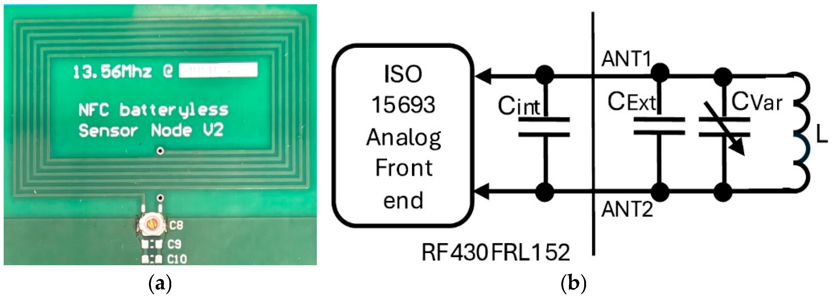
The meandered structure was placed on the top side of the dielectric substrate made of FR4 with a dielectric constant of 4.2 and a loss tangent of 0.02. The feedline placed at the bottom side of the substrate is connected to the antenna structure using one via on each end. NFC works at 13.56 MHz with a 1.8 MHz bandwidth, Thus, tuning the NFC antenna is important not only for data communication but also for power harvesting. The inductance of the antenna, which can be calculated using the equation shown below and external capacitor as shown in Figure 2. The inductance can be calculated as illustrated in Equation (1) below.
L = N × P × μ 0 π × 2 w + h + 2 h 2 + w 2 h × ln h + h 2 + w 2 w w × ln w + h 2 + w 2 w + h × ln 2 × h a + w × ln 2 × w a
where N is the number of turns, P is the correction factor, w is the average width of the rectangle, h is the average height of the rectangle, a is the trace width and μ0 is the permeability of the medium. Equation (1) is the modified Wheeler expression for a planar rectangular spiral inductor, originally derived in [28]. The correction factor P accounts for the rectangular geometry and winding fill ratio of the spiral; the dependence on the average loop dimensions (w, h) reflects the growth of magnetic flux linkage with loop area, and the dependence on N captures the mutual inductance between adjacent turns. Substituting the geometric parameters listed in Table 1 yields a calculated inductance of L = 1.776 µH. After the inductance and the capacitance are tuned, the resonance frequency for this design can be computed by using Equation (2) below.
F r e s o n a n t = 1 2 π × F × C t o t a l
where L is the inductance of the antenna and Ctotal is the total capacitance, which consists of the variable capacitance, CVar, in board and CExt, a variable capacitance with 1–10 pF variability for fine tuning. These are in parallel with the internal capacitors present in the NFC IC, which is 35 pF ±10%, CExt is C9 + C10 two 0805-inch surface mount devices (SMD). It should be noted that C10 and C8 are included only for prototype testing. For a real application, once the required total capacitance is calculated, C9 can either be added to meet that value or eliminated entirely if the antenna inductance is designed to resonate at 13.56 MHz using only the NFC IC’s internal tuning capacitor. In addition to the antenna self-inductance, the magnetic coupling between the reader antenna and the proposed tag antenna determines how efficiently energy is harvested. This coupling is characterized by the coupling coefficient
K = M L r e a d e r   × L t a g
where M is the mutual inductance between the two loops, computed using the Neumann formulation for coaxial rectangular loops and Lreader and Ltag denote the self-inductances of the reader and tag antennas, respectively.
Using the DLP-7970ABP reader antenna dimensions (approximately 47 × 34 mm, Lreader ≈ 1 µH), the proposed tag antenna dimensions (43 × 25 mm), and the operating separation of 30 mm, the coupling coefficient is estimated to be on the order of k ≈ 0.01–0.05. This weak coupling (k << 1) is characteristic of 13.56 MHz NFC operation and motivates the closed-loop power-management scheme proposed in this work, since harvested power scales approximately as k2.
For the NFC transceiver and microcontroller, the RF430FRL152H (Texas Instrument, Dallas, TX, USA) is used which is an all-in-one IC combining the NFC transceiver and a microcontroller. This gives the system a smaller footprint, though a separate NFC transceiver and microcontroller can be used, as shown in [23] where an STM32L03 MCU and ST25DV16K-JFR6D3 NFC transceiver from STMicroelectronics (Geneva, Switzerland) were employed. When choosing an NFC IC, it is much more desirable to select one with integrated NFC harvesting built-in; if not it can be constructed by implementing a full-bridge rectifier.
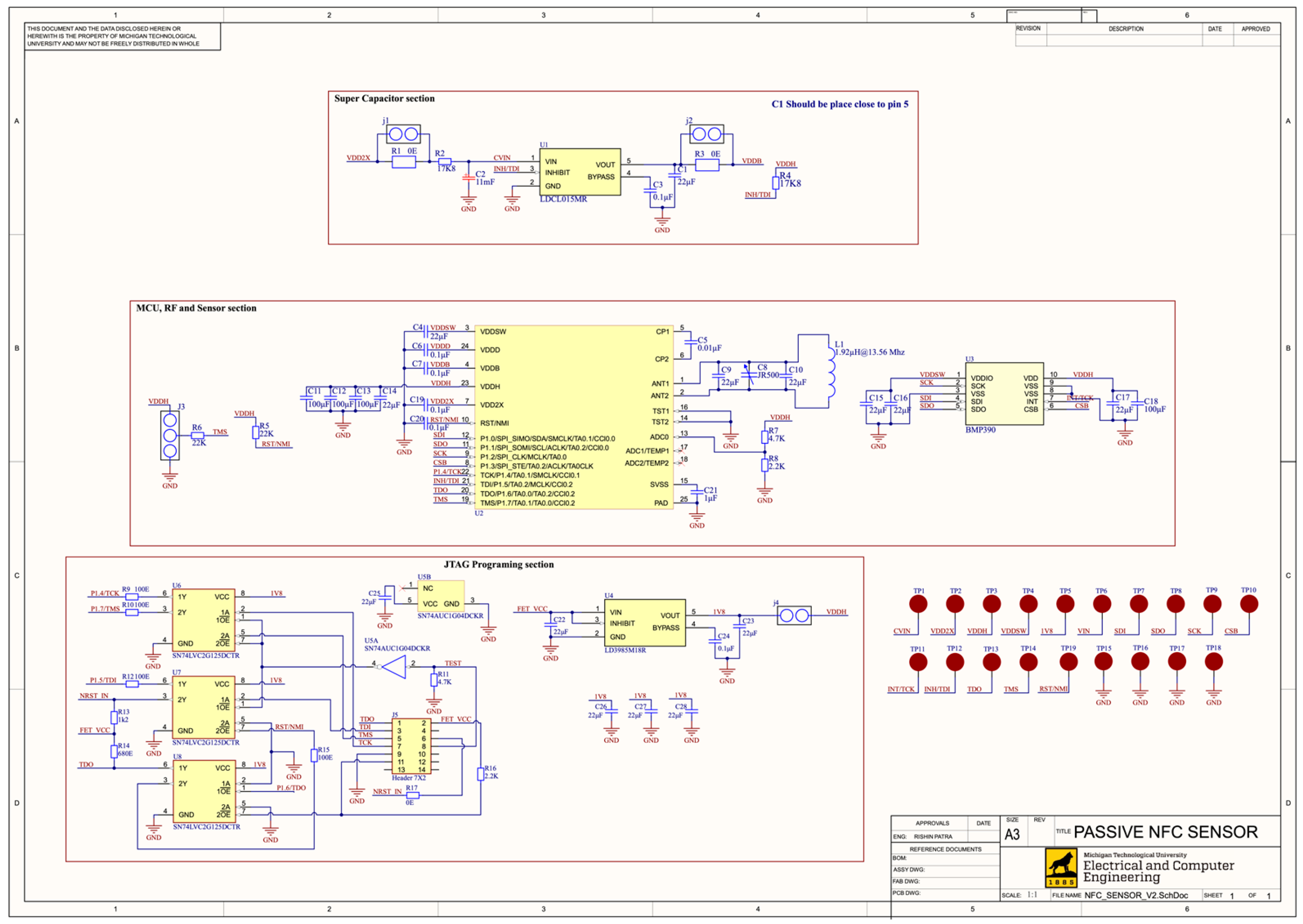
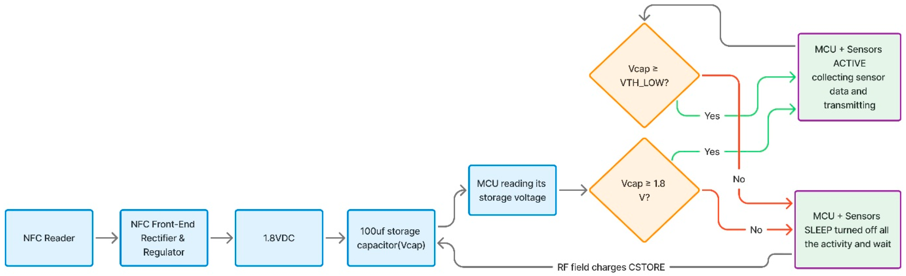
In this system design rectified voltage from the RF analog front end (VDDH) is used since it directs the raw output from the integrated rectifier, which ranges from 1.7 V to 2.1 V. When designing ultra-low-power designs, it is better to avoid using a regulator since even a low dropout (LDO) regulator consumes power. For the sensing unit, the BMP390 from Bosch (Gerlingen, Germany) is used; it is high-precision barometric with pressure and temperature sensor. Additionally, the internal temperature sensor of RF430FRL152H is used. The BMP390 is connected to the microcontroller unit (MCU) using the SPI protocol connection, as shown in the schematic in Figure 3. Power management is a crucial part of this design, as it plays a major role in obtaining obtain a reliable performance. The power-management system is shown in the block diagram presented in Figure 4 below.
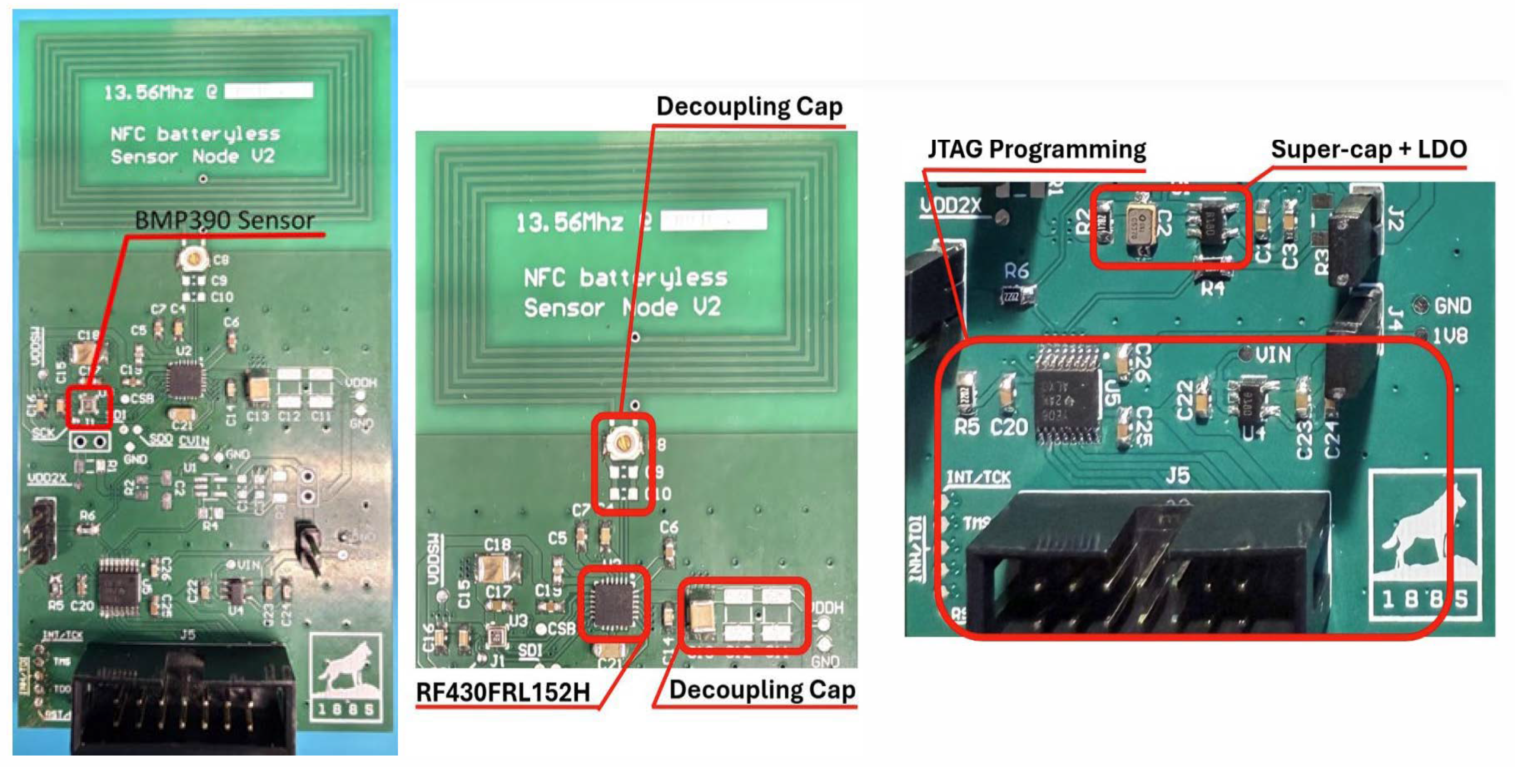
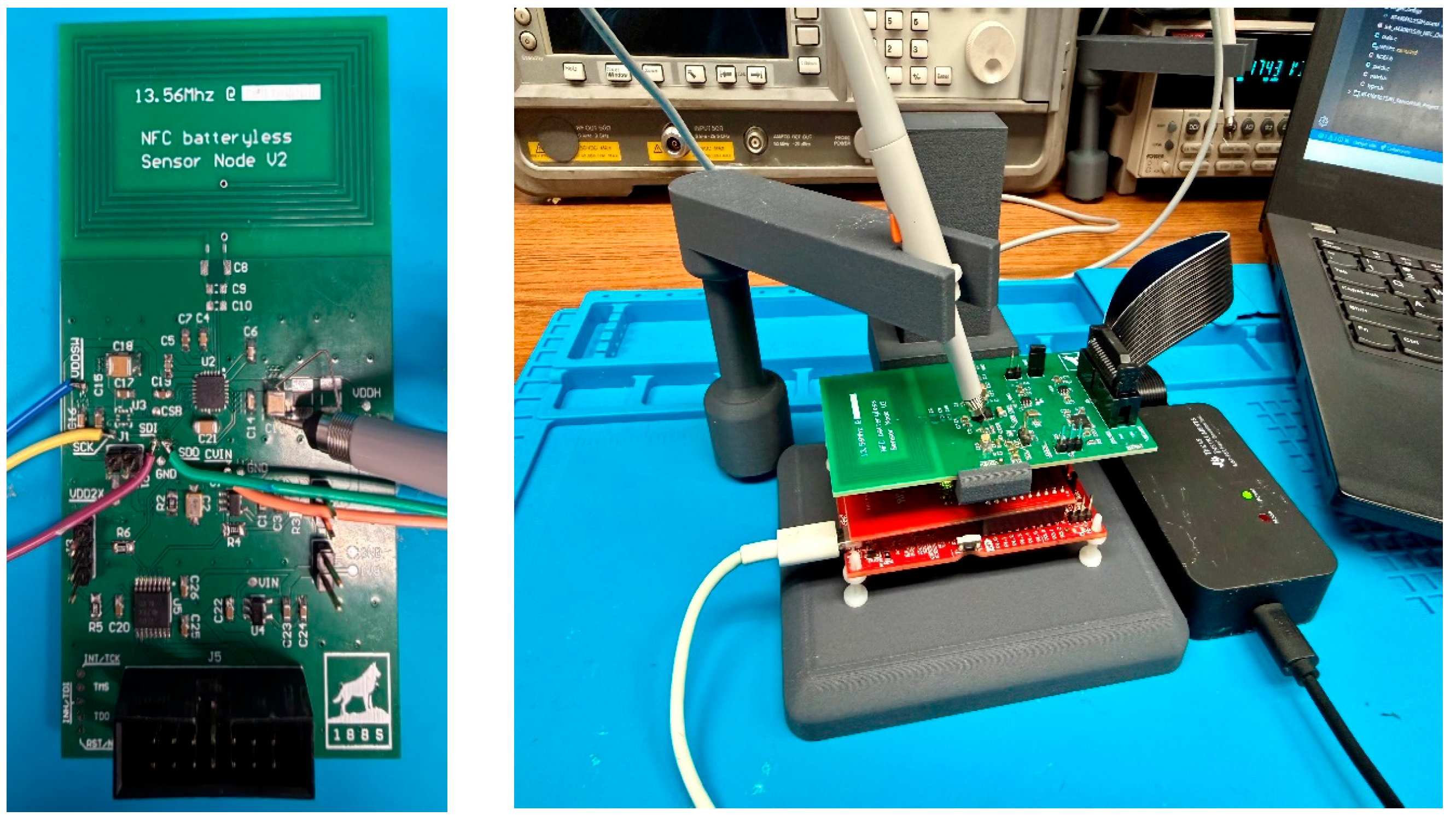
A regulator could have a 0.3 to 0.4 V drop across it; since in our prototype all the Ics, including the sensor can handle 2.1 V, so no LDO was used to maximize power usage. For the voltage feedback, ADC0 or pin13 of the RF430FRL152H is used though a resistor-voltage divider, since the maximum ADC input in this microcontroller is 0.7 V input. Figure 5 shows the hardware prototype of the proposed batteryless NFC multi-sensor node. The top section of the printed circuit board integrates the 13.56 MHz meandered NFC loop antenna, which is tuned for efficient energy harvesting and data communication. The central region hosts the RF430FRL152H NFC transponder with an embedded microcontroller, serving as the core processing and NFC interface unit. A BMP390 temperature and pressure sensor is integrated near the controller to minimize interconnect length and power consumption. Decoupling and energy storage capacitors are strategically placed close to the NFC IC and sensors to stabilize the harvested supply voltage and support transient current demands during sensing and communication. The bottom section of the board includes the JTAG interface for programming and debugging, along with auxiliary power conditioning components used during prototyping and evaluation. This layout reflects a compact and energy-aware hardware integration optimized for batteryless operation under NFC power constraints.
In this design, the MCU reads the voltage across the decoupling capacitor and ensures that it does not reach 1.8 V. Otherwise, it goes into sleep mode and waits for an ADC interrupt; this is done so that during operation the voltage does not drop below the burnout voltage of the sensor and the MCU. The total power consumption of the prototype under a 1.064 mW harvested-power budget is summarized in Table 2.
The maximum number of sensors that the proposed node can support is not determined solely by the average harvested power. It is jointly constrained by three independent limits: (i) the available hardware interfaces of the MCU; (ii) the energy that the storage capacitor can deliver during a single measurement, and (iii) the recharge interval required between measurements.
First, the RF430FRL152H provides a finite set of digital interfaces, namely a single I2C bus, an SPI bus, and a small number of GPIOs and analog inputs. The I2C bus can address multiple sensors using distinct slave addresses, while SPI requires a dedicated chip-select line per device. The maximum number of sensors that can be physically connected is therefore set by the MCU pin/bus configuration; for the present prototype, this corresponds to up to approximately six concurrently addressable I2C devices, or fewer when SPI/analog sensors are mixed in.
Second, even when an interface is available, each sensor activation must fit within the energy stored on the VDDH capacitor between its fully charged voltage Vmax and the MCU brownout threshold Vmin:
E c a p = 1 2 × C × V m a x 2 V m i n 2
For the prototype values Vmax = 1.85 V, Vmin = 1.3 V, and C = 100 µF, this gives Ecap ≈ 86.6 µJ per discharge cycle. A sensor with peak power Psensor and measurement time tmeas is supported only if Psensor x tmeasEcap, or equivalently:
C ≥ (2 × Psensor × tmeas)/(Vmax2Vmin2)
Third, after each activation the capacitor must be replenished from the harvested power, giving a recharge interval:
tcharge ≈ (Psensor × tmeas)/Pharvested
Equation (6) defines the practical limit: as Psensor grows, tcharge grows linearly, and the effective measurement duty cycle drops. As an example, a sensor drawing 50 mW for 1 ms requires 50 µJ per measurement, well within the 86.6 µJ available, with a recharge interval of approximately 47 ms, which is acceptable for periodic sensing applications. By contrast, a sensor drawing 100 mW for 10 ms would demand 1 mJ per measurement, far exceeding the available 86.6 µJ. Supporting it would require either a much larger storage element (in the millifarad range) or a recharge interval of approximately one second between measurements, neither of which is practical for the intended periodic-monitoring use cases.
On this basis, the proposed system can support any combination of sensors that simultaneously
  • Fits the MCU’s available I2C/SPI/GPIO interfaces
  • Draws an average power within the headroom shown in Table 2
  • Have a peak power–time product compatible with the storage capacitor and an acceptable recharge interval. For the present 100 µF design, this corresponds to a peak sensor power envelope of roughly Psensor ≤ 100 mW with sub-millisecond to a few millisecond measurement durations.
The design procedure for this adaptive power management is as follows:
  • The voltage across the decoupling capacitors starts to rise as the reader comes closer to NFC tag.
  • The MCU starts operating in ultra-low power mode as soon as the voltage reaches 1.1 V. It then checks the ADC0 pin to determine if it is at 1.8V; if not, it goes back to deep sleep for 0.1 ms.
  • It wakes up after 0.1 ms to check if the voltage has reached 1.8 V. If not the process repeats; if it has, it proceeds to the next step.
  • When the voltage reaches 1.8 V it starts collecting data while monitoring the voltage.
  • In any case, if the voltage falls below a set point which in prototype 1.3 V, since the BMP390 stops working below 1.2 V, the MCU saves the already collected data, goes back to sleep and waits for the decoupling capacitor to charge again.

3. Results and Analysis

The fabricated prototype is shown in Figure 6. The software version 1 is flashed using a JTAG connected to the Mixed-Signal Processor Flash Emulation Tool (MSP-FET) a programmer and a debugger from Texas Instrument. For testing, the sensor from BMP390 was set to ultra-high-resolution mode with the oversampling setting enabled. Two readers were used during characterization. The primary reader was the Texas Instruments DLP-7970ABP NFC/RFID BoosterPack (built around the TRF7970A multi-protocol NFC transceiver), interfaced with the MSP-EXP430FR4133 LaunchPad development board. A consumer NFC-enabled smartphone was also used to verify interoperability with off-the-shelf reader hardware.
Voltage and current at the harvested power output were measured using a Keithley digital multimeter, and the reader-to tag separation was set using a 3D-printed custom linear positioning stage.
The harvested power was measured as follows. The NFC tag was positioned coaxially with the DLP-7970ABP reader antenna at a separation of 20 mm. A 100 Ω resistive load was connected across the VDDH node, replacing the MCU and sensor supply path. This load value was selected based on initial bench characterization as the operating point yielding the maximum V × I product within the available current capacity. The steady-state voltage across the load was measured using a digital multimeter (Keithley 2000, Keithley Instruments, Cleveland, OH, USA), and the corresponding current was obtained as I = V/R, giving the reported 1.064 mW (1.85 V × 560 µA). The reader was operated in compliance with the ISO/IEC 15693 standard. The measurement was repeated N = 10 times under identical conditions, with trial-to-trial variation falling within the resolution of the multimeter.
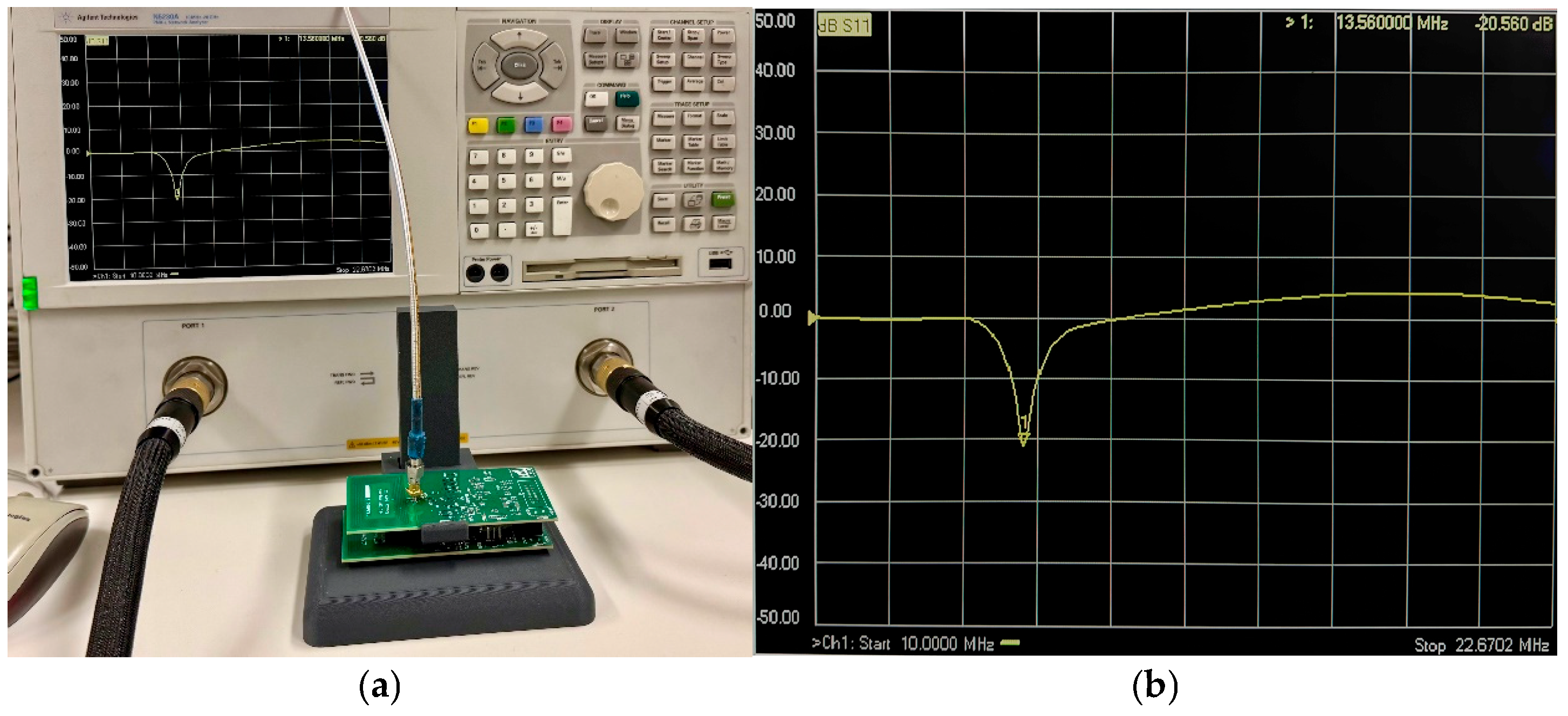
To measure the resonant frequency and quality factor, a vector network analyzer (Agilent Technologies N5230A, Agilent Technologies, Santa Clara, CA, USA) was used. For antenna characterization, the prototype sensing antenna was positioned at a 2 cm separation, as shown in Figure 7a. The measured S11 response shows a resonance frequency of 13.56 MHz, as illustrated in Figure 7b. The Q-factor of the loop antenna at the 13.56 MHz resonance was determined from the −3 dB bandwidth of the S11 response using Q = f0/Δf−3 dB, yielding a measured Q-factor of approximately Q ≈ 62, which is consistent with values reported for compact 13.56 MHz loop antennas of similar geometry.
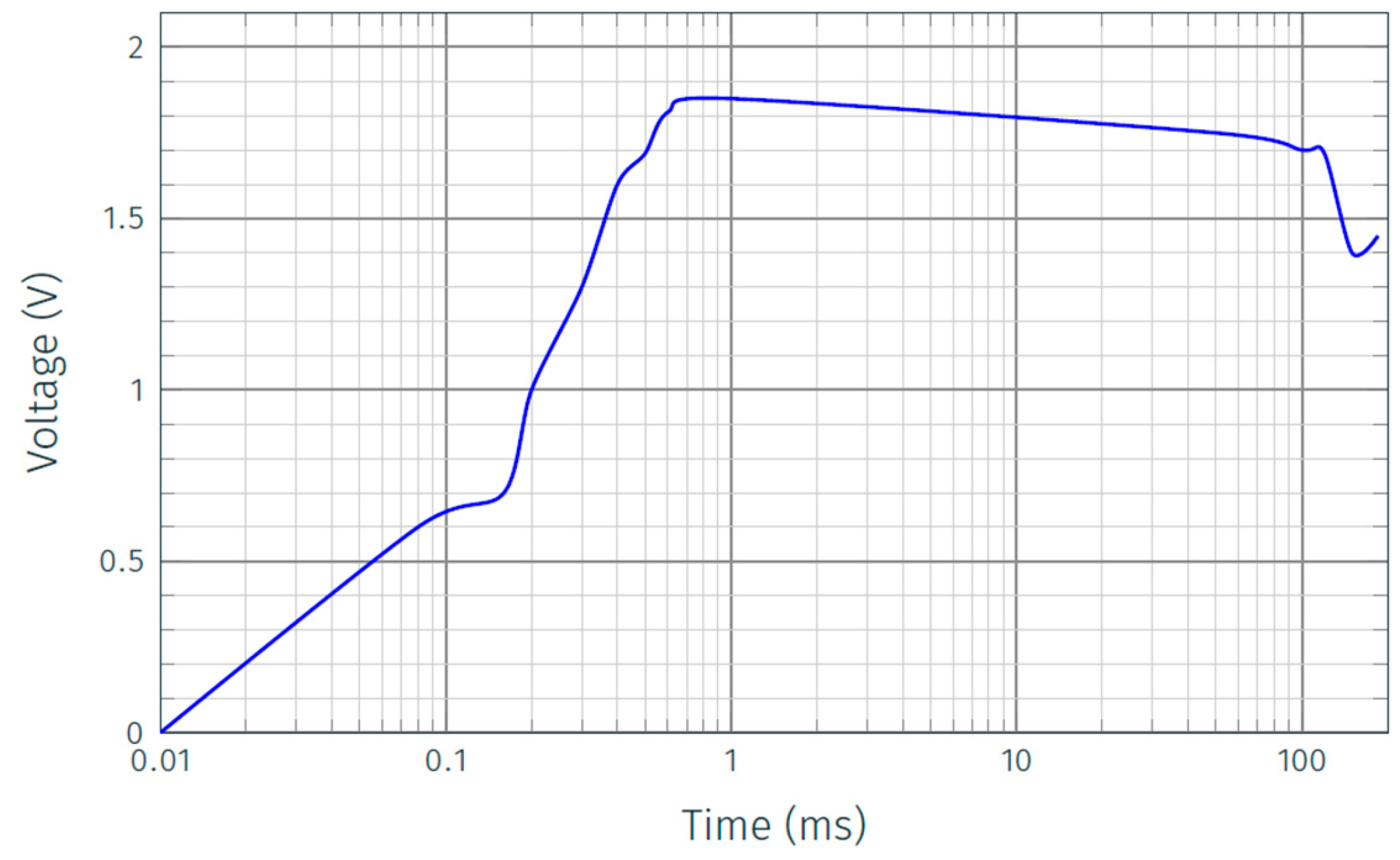
To measure the voltage across the decoupling capacitor and determine how the system is performing oscilloscope probe was connected across C13, a 100 μF capacitor close to the MCU. For the probe, a low impedance ground pin was used to lower noise, and the signal was averaged over 1000 samples, the result is shown in Figure 8. The voltage rise across the 100 µF storage capacitor is well described by a first order charging response driven by the harvested current source. Modeling the NFC front end as an ideal current source Ih = 560 µA charging the capacitor C, the time required to reach a target voltage V is given by:
t = C × V/Ih
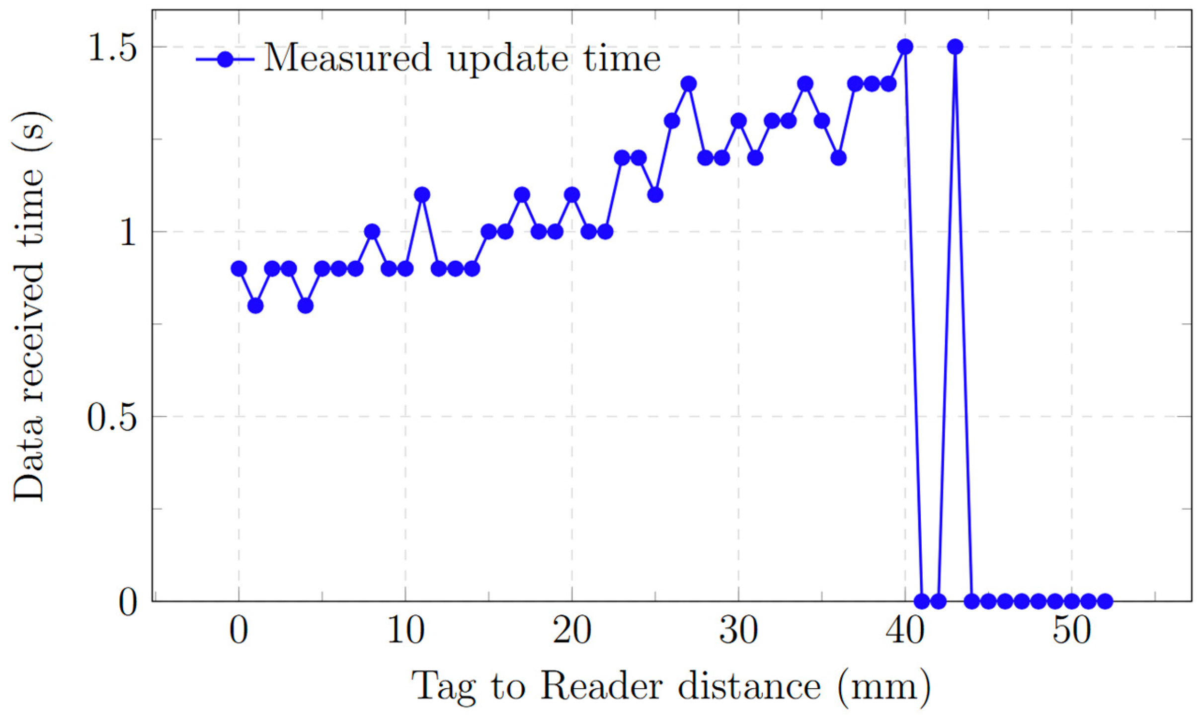
Substituting C = 100 µF, V = 1.8 V (the MCU operating threshold), and Ih = 560 µA yields a calculated rise time of approximately t ≈ 321 ms. The measured rise time observed in Figure 8 is approximately 0.5 s, in reasonable agreement with the ideal first order prediction. The small deviation between the calculated and measured values is attributed to rectifier turn-on delay at low input voltages and to the finite output impedance of the harvester, both of which are typical characteristics of practical 13.56 MHz RF-to-DC energy harvesting front ends. Once Vc reaches the 1.8 V operating threshold, the closed-loop power management scheme triggers sensor activation and NFC data transmission, after which the cycle repeats. Specifically, when the threshold of 1.8 V is met, data acquisition starts and the results are transmitted to the reader after 150 ms. For consistency, the response time is defined as the interval between the moment the NFC tag enters the reader’s field and the moment the first successfully decoded ISO/IEC 15693 data frame containing a valid sensor measurement is received at the reader. Figure 9 presents the measured data update (response) time versus distance. As the separation between the NFC tag and reader increases, the update time gradually rises due to reduced magnetic coupling and lower harvested power. The maximum reading range is defined as the largest reader-to-tag separation at which ten consecutive ISO/IEC 15693 reads succeed without error. Stable data transmission is maintained up to approximately 40 mm, beyond which the harvested energy becomes insufficient to sustain reliable operation, resulting in transmission dropouts.
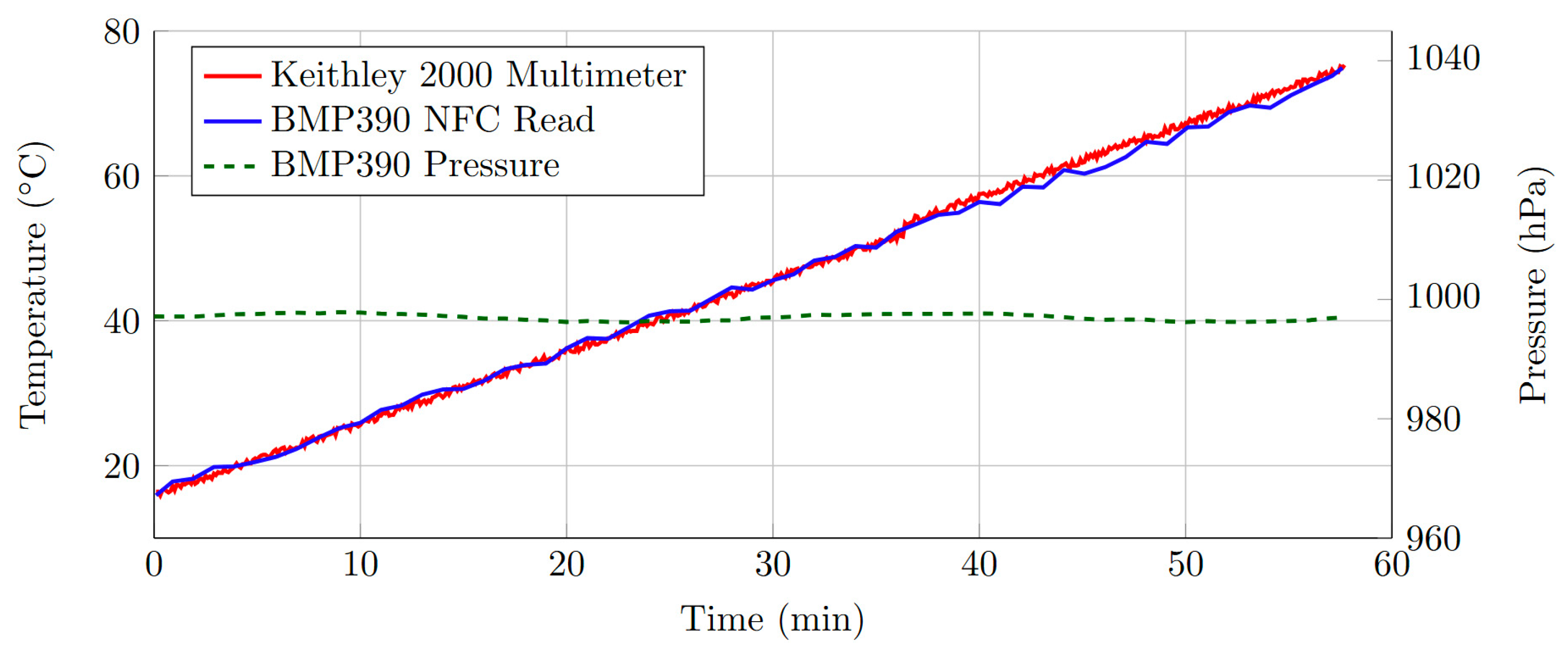
These results demonstrate the effectiveness of the proposed adaptive power-management strategy in maintaining reliable sensing and communication over the achievable wireless operating range. Figure 10 presents a comparison between the temperature data acquired by the proposed batteryless NFC sensor node using the BMP390 sensor and reference measurements obtained from a calibrated Keithley 2000 multimeter. The measurements were conducted with the NFC tag positioned 30 mm from the reader. The temperature readings obtained via NFC closely track the reference measurements over the full measurement duration. This confirms the accuracy and reliability of the BMP390 temperature sensing and NFC-based data transmission under continuous batteryless operation, powered solely by harvested RF energy. Simultaneously, the pressure data obtained from the BMP390 sensor remains stable over the entire measurement duration, exhibiting only minor variations consistent with ambient environmental conditions. This demonstrates the reliable acquisition and NFC-based wireless transmission of pressure data under continuous batteryless operation at a reader distance of 30 mm.
For the type of measurements reported in Figure 9 and Figure 10, the plotted quantities, harvested voltage, current, and response time, as a function of reader-to-tag distance are deterministic with respect to the measurement geometry: at a fixed distance, the magnetic field, harvested voltage, and resulting current are governed by RF-to-DC rectifier physics and do not exhibit trial-to-trial statistical variation beyond instrument-level quantization. This is consistent with how comparable batteryless NFC characterization plots are reported in the recent literature [12]. The instrument-level uncertainties associated with these measurements are smaller than the marker size used in Figure 9 and Figure 10. Where statistical variation is genuinely meaningful, namely the accuracy of the BMP390 sensor readings against the reference Keithley 2000 measurements shown in Figure 10, the residuals between the sensor and reference are visible directly in the overlay plot.

4. Comparison

Table 3 compares the proposed batteryless NFC multi-sensor system with previously reported NFC-based sensing platforms in [18,19,20,21,22,23,24]. The comparison considers key metrics, including the employed microcontroller unit (MCU), antenna size, harvested voltage and current levels, NFC response time, sensing application, wireless operating range, and power-management strategy.
Most existing works utilize ultra-low-power MCUs such as RF430FRL152H, ATtiny variants, ATSAMD21, and STM32L03, demonstrating the feasibility of batteryless NFC sensing across a wide range of applications, including strain and temperature sensing [18], gas sensing [19,22], force sensing [20], conductivity and temperature sensing [22], humidity sensing [22,23], and pH sensing [24]. However, a common characteristic across all reported systems in [18,19,20,21,22,23,24] is the absence of an active power management mechanism, with most designs operating without voltage regulation or feedback-based control. This limits their robustness under fluctuating harvested- power conditions and restricts scalability to multi-sensor operation. In addition, several prior works omit critical NFC response timings; specifically, the NFC response time was not provided in [18,20,22,23,24], making it difficult to assess the dynamic performance of these systems. Even in cases where response time was reported, such as in [19] (5000 ms) and [22] (~1 s), the values remain relatively long, which may limit applicability in time-sensitive sensing scenarios. Similarly, harvested voltage and current levels were either not reported or were limited to lower current values in multiple studies, constraining the supported sensor types and measurement frequency. From an antenna and wireless range perspective, previously reported designs achieve maximum read distances ranging from approximately 8 mm to 43 mm, depending on antenna size and number of turns. While larger antennas generally enable increased wireless range, they introduce a larger footprint, as seen in [21,24]. Compact designs, such as that in [20], exhibit significantly reduced read ranges.
In addition to the performance comparison shown in Table 3, a component-level cost analysis was carried out to compare the proposed prototype with the reference design in [22]. The bill of materials of the proposed prototype is summarized in Table 4 below. The design in [22] follows a two-chip architecture in which a discrete NFC tag IC (ST25DV-series, ~$1.10) is paired with a separate microcontroller (ARM Cortex-M0+, e.g., ATSAMD21G18A, ~$3.50). Together with additional sensors and signal-conditioning components, the estimated bare component cost is in the range of $10–14. The proposed prototype achieves a lower cost of approximately $8.00 because the single RF430FRL152H IC integrates both the NFC transceiver and the MSP430 microcontroller in one package, eliminating the cost and board area of a separate MCU as well as the associated inter-chip interconnects. In contrast, the proposed system integrates a voltage feedback-based closed-loop power-management strategy, which is not reported in any of the works compared.
By monitoring the storage capacitor voltage and enabling sensing operations only when sufficient energy is available, the proposed approach ensures stable operation under limited harvested power. This enables reliable multi-sensor functionality, supporting temperature, pressure, and altitude sensing within a single platform. Furthermore, the proposed design achieves a response time of 800–1500 ms, which is faster than or comparable to reported systems while providing a maximum wireless operating range of approximately 45 mm, the largest among the compared designs. This performance is achieved with a compact antenna size of 43 mm × 25 mm (6 turns) and a harvested voltage/current of 1.8 V/560 µA, highlighting the effectiveness of the closed-loop power-management scheme.
Overall, the comparison demonstrates that while earlier NFC-based sensing systems successfully validated batteryless operation, they generally lack response time characterization and active power management. The proposed system addresses these limitations by enabling a faster response, an extended wireless range, and reliable multi-sensor operation, thereby advancing the practicality of batteryless NFC sensing platforms.

5. Applicable Scenarios and Environmental Limitations

The proposed batteryless NFC multi-sensor node operates entirely from RF energy harvested during reader proximity and is therefore best suited to intermittent reading scenarios in which a reader can be brought within the ~40 mm operating range at the time of measurement.
The system is well suited to:
  • Cold chain and logistics monitoring, where temperature and pressure conditions are verified during warehouse audits or arrival inspections, especially for disposable packaging where batteryless operation is essential [29].
  • Smart packaging, where periodic quality checks at delivery or shelf inspection are performed by tapping a smartphone to the tag [30].
  • Industrial inspection, where technicians acquire data from sensor nodes during scheduled maintenance rounds [31].
  • Environmental and structural monitoring, where periodic readings are taken during routine walk-throughs without battery replacement, which is particularly advantageous in hard-to-access locations [32].
Conversely, the system is not suitable for:
  • Continuous real-time monitoring, such as always-on vital sign telemetry, which requires sustained energy availability and uninterrupted reader presence [33].
  • High-rate sensing such as vibration or acoustic capture, where sample rates and active-mode duty cycles exceed the energy and recharge limits described in Section 2 [34].
  • Always-on industrial condition monitoring, where continuous data steams are required [35].
  • Long range or unattended deployments, since data acquisition requires a reader within ~40 mm of the tag. Such applications are better served by an active or hybrid NFC-plus-battery design [36].
In summary, the proposed prototype is most useful in periodic, reader present, low duty-cycle measurement scenarios, where the elimination of batteries and the resulting maintenance-free operation outweigh the limitations of intermittent data availability.
In addition to the deployment scenarios outlined above, the proposed system is sensitive to several categories of environmental effects. Because the proposed system operates at 13.56 MHz and relies on inductive coupling between the reader and tag antennas, its performance influenced by three categories of environmental effects.
  • Metal surfaces: When the tag is placed directly on a metallic surface, eddy currents induced in the metal absorb the magnetic field and detune the antenna, reducing harvested power and read range. For metal-mount deployments, a thin ferrite isolator (typically 0.1–0.3 mm of NiZn or MnZn) is required between the tag and the metallic substrate to restore acceptable coupling. For non-metallic mounting, such as plastic, cardboard, glass, fabric, or biological tissue, no shielding is required and the prototype operates as characterized in Section 3.
  • Co-channel 13.56 MHz interference: In environments with multiple HF readers, overlapping reader fields can corrupt ISO/IEC 15693 framing. The ISO/IEC 15693 anti-collision protocol addresses multiple tags within a single field but not overlapping fields, so physical separation between readers or time-division operation is recommended in dense deployments.
  • Industrial EMI: Broadband noise from switching power supplies, motors, and variable frequency drives can degrade the signal-to-noise margin at the RF front end. Measurements in this work were performed in a standard indoor laboratory; reliable operation in heavy industrial settings may require additional PCB-level shielding or careful relocation away from dominant EMI sources.
Overall, the prototype performs as characterized in Section 3 under non-metallic mounting (or ferrite-shielded mounting on metal), absence of overlapping 13.56 MHz fields, and a typical office or laboratory EMI environment. Deployment outside these assumptions requires the corresponding mitigations and may further constrain the scenarios outlined in Section 5.

6. Conclusions and Future Work

This work presented the design and experimental validation of a batteryless NFC multi-sensor node incorporating an adaptive, closed-loop power-management strategy for reliable wireless sensing. The system was designed to operate exclusively from energy harvested at 13.56 MHz, eliminating the need for batteries while ensuring stable operation under the limited and variable power conditions inherent to NFC-based energy harvesting. The proposed platform integrates an ISO/IEC 15693-compliant RF430FRL152H NFC transponder with a compact, tuned loop antenna and energy-aware firmware that continuously monitors the storage capacitor voltage. Sensor acquisition and NFC transmissions are initiated only when sufficient energy is available, preventing brownout events and enabling dependable multi-sensor functionality. A BMP390 temperature and pressure sensor, together with the internal temperature sensor of the microcontroller, were used to validate system operation under varying power demands. Experimental results confirm that the system successfully harvests 1.064 mW of power, delivering an output voltage of 1.85 V and a current of 560 µA. The prototype achieves a wireless operating range of up to 40–41 mm and a response time of approximately 800 ms, demonstrating reliable sensing, data logging, and NFC communication powered entirely by harvested RF energy. Overall, the results demonstrate that combining a tuned NFC antenna, efficient energy harvesting, and voltage-feedback-based power management enables a compact and reliable batteryless multi-sensor node. The proposed architecture provides an effective foundation for maintenance-free NFC sensing platforms intended for low-power temperature and pressure monitoring applications.
Future work will focus on (i) extending the platform to support additional sensor modalities such as humidity, gas, and electrochemical sensors; (ii) integrating a flexible or printed antenna for wearable form factors; (iii) investigating adaptive tuning circuits to mitigate detuning caused by nearby metallic or biological media; and (iv) developing a lightweight on-chip data-compression scheme to reduce NFC transmission time and further lower energy required per measurement cycle.

Author Contributions

Conceptualization, R.P. and J.W.C.; methodology, R.P.; software, R.P.; validation, R.P. and H.S.N.C.; formal analysis, R.P. and H.S.N.C.; investigation, R.P.; resources, J.W.C.; data curation, R.P.; writing—original draft preparation, R.P.; writing—review and editing, H.S.N.C. and J.W.C.; visualization, R.P.; supervision, J.W.C.; project administration, J.W.C.; funding acquisition, J.W.C. All authors have read and agreed to the published version of the manuscript.

Funding

This work was supported in part by National Science Foundation (Award ID: 2335149).

Data Availability Statement

The data presented in this study is available on request from the corresponding author.

Conflicts of Interest

The authors declare no competing interests.

Abbreviations

The following abbreviations are used in this manuscript:
NFCNear field communication
MCUMicro controller unit
PCBPrinted circuit board

References

  1. West, H.; Quinn, N.; Horswell, M. Remote sensing for drought monitoring and impact assessment: Progress, past challenges and future opportunities. Remote Sens. Environ. 2019, 232, 111291. [Google Scholar] [CrossRef] [Scilit]
  2. Weiss, M.; Jacob, F.; Duveiller, G. Remote sensing for agricultural applications: A meta-review. Remote Sens. Environ. 2020, 236, 111402. [Google Scholar] [CrossRef] [Scilit]
  3. Zeng, J.; Long, D.; Zhang, Y.; Ryu, D.; Wigneron, J.-P.; Huang, Q. Emerging remote sensing techniques for hydrological applications. Remote Sens. Environ. 2025, 332, 115060. [Google Scholar] [CrossRef] [Scilit]
  4. Sun, X.; Zhao, C.; Li, H.; Yu, H.; Zhang, J.; Qiu, H.; Liang, J.; Wu, J.; Su, M.; Shi, Y.; et al. Wearable near-field communication sensors for healthcare: Materials, fabrication and application. Micromachines 2022, 13, 784. [Google Scholar] [CrossRef] [Scilit]
  5. Aldana-Martín, J.F.; García-Nieto, J.; Roldán-García, M.M.; Aldana-Montes, J.F. Semantic modelling of Earth observation remote sensing. Expert Syst. Appl. 2022, 187, 115838. [Google Scholar] [CrossRef] [Scilit]
  6. Kordzadeh, A.; Holzmann, D.; Binder, A.; Moldaschl, T.; Sturm, J.; Roshanghias, A. Miniaturized on-chip NFC antenna versus screen-printed antenna for the flexible disposable sensor strips. IoT 2020, 1, 309–319. [Google Scholar] [CrossRef] [Scilit]
  7. Aziza, H. NFC technology in mobile phone next-generation service. In Proceedings of the 2nd International Workshop on Near Field Communication, Monaco, Monaco, 20 April 2010; IEEE: Piscataway, NJ, USA, 2010; pp. 21–26. [Google Scholar]
  8. Zou, H.; Zhou, Z.; Huang, M.; Li, W.; Yang, B.; Zhao, X.; Li, T.; Xu, L.; Wang, T.; Wang, L. NFC/RFID-enabled wearables and implants for biomedical applications. Microsyst. Nanoeng. 2025, 11, 191. [Google Scholar] [CrossRef] [Scilit]
  9. Paret, D. Design Constraints for NFC Devices; Wiley: Hoboken, NJ, USA, 2016. [Google Scholar]
  10. Choi, J.; Visagie, I.; Chen, Y.; Abbel, R.; Parker, K. NFC-enabled dual-channel flexible printed sensor tag. Sensors 2023, 23, 6765. [Google Scholar] [CrossRef] [Scilit]
  11. Olenik, S.; Lee, H.S.; Güder, F. The future of near-field communication-based wireless sensing. Nat. Rev. Mater. 2021, 6, 286–288. [Google Scholar] [CrossRef] [Scilit]
  12. Lazaro, A.; Villarino, R.; Girbau, D. A survey of NFC sensors based on energy harvesting for IoT applications. Sensors 2018, 18, 3746. [Google Scholar] [CrossRef] [Scilit] [PubMed]
  13. Kang, M.H.; Lee, G.J.; Yun, J.H.; Song, Y.M. NFC-based wearable optoelectronics working with smartphone application for untact healthcare. Sensors 2021, 21, 878. [Google Scholar] [CrossRef] [Scilit]
  14. Fischbacher, R.; Görtschacher, L.; Auinger, B.; Bösch, W.; Grosinger, J. Batteryless NFC sensor tag for temperature threshold monitoring. In Proceedings of the International Symposium on Antennas and Propagation (ISAP), Incheon, Republic of Korea, 4–7 November 2024; IEEE: Piscataway, NJ, USA, 2024; pp. 1–2. [Google Scholar] [CrossRef] [Scilit]
  15. Lazaro, A.; Boada, M.; Villarino, R.; Girbau, D. Color measurement and analysis of fruit with a Batteryless NFC sensor. Sensors 2019, 19, 1741. [Google Scholar] [CrossRef] [Scilit]
  16. Lazaro, A.; Villarino, R.; Lazaro, M.; Canellas, N.; Prieto-Simon, B.; Girbau, D. Recent advances in batteryless NFC sensors for chemical sensing and biosensing. Biosensors 2023, 13, 775. [Google Scholar] [CrossRef] [Scilit]
  17. Lin, R.; Kim, H.J.; Achavananthadith, S.; Kurt, S.A.; Tan, S.C.C.; Yao, H.; Tee, B.C.K.; Lee, J.K.W.; Ho, J.S. Wireless battery-free body sensor networks using near-field-enabled clothing. Nat. Commun. 2020, 11, 444. [Google Scholar] [CrossRef] [Scilit] [PubMed]
  18. Escobedo, P.; Bhattacharjee, M.; Nikbakhtnasrabadi, F.; Dahiya, R. Smart bandage with wireless strain and temperature sensors and batteryless NFC tag. IEEE Internet Things J. 2021, 8, 5093–5100. [Google Scholar] [CrossRef] [Scilit]
  19. Salehnia, F.; Lazaro, A.; Villarino, R.; Lazaro, M.; Canyellas, N.; Vilanova, X.; Llobet, E.; Girbau, D. Battery-free NFC sub-ppm gas sensor for distributed gas monitoring applications at room temperature. IEEE J. Radio Freq. Identif. 2023, 7, 630–643. [Google Scholar] [CrossRef] [Scilit]
  20. Boada, M.; Lazaro, A.; Villarino, R.; Gil-Dolcet, E.; Girbau, D. Batteryless NFC bicycle tire pressure sensor based on a force-sensing resistor. IEEE Access 2021, 9, 103975–103987. [Google Scholar] [CrossRef] [Scilit]
  21. Lazaro, A.; Villarino, R.; Pacios, M.; Lazaro, M.; Canellas, N.; Girbau, D.; Prieto-Simon, B. Batteryless NFC conductivity sensor for bovine mastitis detection in farming 4.0. IEEE Access 2024, 12, 45824–45838. [Google Scholar] [CrossRef] [Scilit]
  22. Jalajamony, H.M.; De, S.; Fernandez, R.E. NFC-enabled batteryless AI-integrated sensing network for smart PPE system. IEEE Sens. J. 2024, 24, 26914–26925. [Google Scholar] [CrossRef] [Scilit]
  23. Kumar, S.; Gawade, D.R.; Simorangkir, R.B.V.B.; Moloudian, G.; Belcastro, M.; Torchia, P.; Federico, A.; Buckley, J.L.; O’Flynn, B. A Batteryless contact lens sensor prototype with enhanced performance for cattle health monitoring. In Proceedings of the IEEE Sensors Applications Symposium (SAS), Naples, Italy, 23–25 July 2024; IEEE: Piscataway, NJ, USA, 2024; pp. 1–5. [Google Scholar]
  24. Boada, M.; Lazaro, A.; Villarino, R.; Girbau, D. Batteryless NFC sensor for pH monitoring. IEEE Access 2019, 7, 33226–33239. [Google Scholar] [CrossRef] [Scilit]
  25. Lazaro, A.; Boada, M.; Villarino, R.; Girbau, D. Batteryless smart diaper based on NFC technology. IEEE Sens. J. 2019, 19, 10848–10858. [Google Scholar] [CrossRef] [Scilit]
  26. ISO/IEC 15693:2019; Cards and Security Devices for Personal Identification — Contactless Vicinity Objects. International Organization for Standardization: Geneva, Switzerland, 2019.
  27. ISO/IEC 14443:2018; Cards and Security Devices for Personal Identification — Contactless Proximity Objects. International Organization for Standardization: Geneva, Switzerland, 2018.
  28. Mohan, S.S.; del Mar Hershenson, M.; Boyd, S.P.; Lee, T.H. Simple accurate expressions for planar spiral inductances. IEEE J. Solid-State Circuits 1999, 34, 1419–1424. [Google Scholar] [CrossRef] [Scilit]
  29. Jedermann, R.; Ruiz-Garcia, L.; Lang, W. Spatial temperature profiling by semi-passive RFID loggers for perishable food transportation. Comput. Electron. Agric. 2009, 65, 145–154. [Google Scholar] [CrossRef] [Scilit]
  30. Catarinucci, L.; De Donno, D.; Mainetti, L.; Palano, L.; Patrono, L.; Stefanizzi, M.L.; Tarricone, L. An IoT-aware architecture for smart healthcare systems. IEEE Internet Things J. 2015, 2, 515–526. [Google Scholar] [CrossRef] [Scilit]
  31. Want, R. An introduction to RFID technology. IEEE Pervasive Comput. 2006, 5, 25–33. [Google Scholar] [CrossRef] [Scilit]
  32. Sample, A.P.; Yeager, D.J.; Powledge, P.S.; Mamishev, A.V.; Smith, J.R. Design of an RFID-based battery-free programmable sensing platform. IEEE Trans. Instrum. Meas. 2008, 57, 2608–2615. [Google Scholar] [CrossRef] [Scilit]
  33. Bennett, T.R.; Massey, B.; Wu, J.; Hayes, S.A.; Jafari, R. Motionsynthesis toolset (MoST): A toolset for human motion data synthesis and validation. In Proceedings of the 4th ACM MobiHoc Workshop on Pervasive Wireless Healthcare, Philadelphia, PA, USA, 11 August 2014; Association for Computing Machinery: New York, NY, USA, 2014; pp. 25–30. [Google Scholar] [CrossRef] [Scilit]
  34. Lu, X.; Wang, P.; Niyato, D.; Kim, D.I.; Han, Z. Wireless networks with RF energy harvesting: A contemporary survey. IEEE Commun. Surv. Tutor. 2015, 17, 757–789. [Google Scholar] [CrossRef] [Scilit]
  35. Lee, J.; Bagheri, B.; Kao, H.-A. A cyber-physical systems architecture for Industry 4.0-based manufacturing systems. Manuf. Lett. 2015, 3, 18–23. [Google Scholar] [CrossRef] [Scilit]
  36. Want, R. Near field communication. IEEE Pervasive Comput. 2011, 10, 4–7. [Google Scholar] [CrossRef] [Scilit]
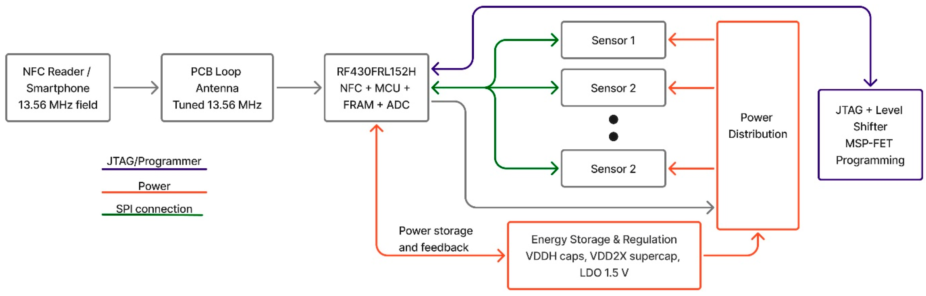
Figure 1. Block diagram of the system containing NFC sensor.
Jsan 15 00042 g001
Figure 2. Designed NFC antenna: (a) PCB antenna that was designed with C8 being the variable capacitor, C9 and C8 for external tuning capacitors and, (b) antenna connected to NFC transceiver IC.
Jsan 15 00042 g002
Figure 3. Schematic diagram of the hardware.
Jsan 15 00042 g003
Figure 4. Power management diagram.
Jsan 15 00042 g004
Figure 5. Picture of the fully populated hardware prototype.
Jsan 15 00042 g005
Figure 6. Fabricated prototype and testing setup.
Jsan 15 00042 g006
Figure 7. (a) Antenna measurement setup, and (b) resonance frequency.
Jsan 15 00042 g007
Figure 8. VDDH voltage curve vs. time.
Jsan 15 00042 g008
Figure 9. Data refresh rate at different distance between the reader and the sensor antennas.
Jsan 15 00042 g009
Figure 10. Obtained results of the developed NFC hardware sending measured temperature and pressure data from BMP390 at 30 mm from the reader reliably. For reference, a separate calibrated temperature probe was used.
Jsan 15 00042 g010
Table 1. Geometric and electrical parameters for inductance calculation.
ParameterValue
Number of turns, N6
Average Width, w37 mm
Average height, h19 mm
Outer height, hout25 mm
Outer width, wout43 mm
Inner height, hin13 mm
Inner width, win31 mm
Trace width, a0.5 mm
Correction factor, P1.8
Measured inductance, Lmeas1.8 μH
Calculated inductance, Lcalc1.776 ×10−6 H
Internal resonance capacitor, CINT35 pF (±10%)
Table 2. Power consumption budget.
ComponentModeVoltageCurrentPower
RF430FRL152H (MCU + NFC)Active (RX/TX)1.8 V350 µA630 µW
RF430FRL152HStandby (LPM3)1.8 V~2 µA~3.6 µW
BMP390 (pressure/temp)Forced measurement1.8 V3.4 µA avg6.1 µW
Voltage divider (ADC sense)Continuous1.8 V5 µA9 µW
Total used by current design~649 µW
Total available (harvested)1.85 V560 µA1064 µW
Average headroom~415 µW
Table 3. Comparison with existing NFC-based sensing systems.
Ref. No.MCUAntenna Size (mm2)Voltage/CurrentNFC
Response Time
Sensing
Application
Wireless
Range
(mm)
Power
Management
Method
[18]RF430FRL152H26 mm × 26 mm
(7 turns)
1.5 V/
450 μA
Not GivenStrain and temperatureMax ~43None
[19]ATTiny1614Not Given
(6 turns)
1.5 V/
450 μA
5000 msGas
Sensing (NO2)
Max ~32None
[20]ATTINY8512 mm × 16 mm
(3 turns)
1.5 V/
450 μA
Not GivenForce sensingMax ~8None
[21]ATTINY161440 mm × 40 mm
(6 turns)
2.5 V~<1 sconductivity and temperatureMax ~20None
[22]ATSAMD21G1829 mm diameter
(5 turns)
3.6 V/
2.5 mA
Not GivenGas and HumidityMax ~40None
[23]STM32L031G6U625 mm diameter
(19 turns)
Not GivenNot GivenTemperature and relative humidityMax ~12None
[24]Attiny8550 mm × 50 mm
(6 turns)
Not GivenNot GivenPH SensorMax ~18None
This workRF430FRL152H43 mm × 25mm
(6 turns)
1.8 V/
560 μA
800 ms to 1500 ms2× Temp, Pressure, Altitude sensorMax ~45Voltage feed-
back close loop
Table 4. Bill of Materials of the Proposed Prototype.
ItemPart/DescriptionUnit Cost (USD)
MCU + NFC transceiver (single chip)RF430FRL152HCRGER (Texas Instruments)$4.05
Pressure/temperature sensorBMP390 (Bosch)$3.15
Passives (decoupling and tuning capacitors, voltage divider resistors)Standard 0402/0603 SMD$0.30
PCB (FR4, 2-layer, 50 × 25 mm, with integrated NFC loop antenna)Standard board shop pricing$0.50
Total component cost$8.00
Disclaimer/Publisher’s Note: The statements, opinions and data contained in all publications are solely those of the individual author(s) and contributor(s) and not of MDPI and/or the editor(s). MDPI and/or the editor(s) disclaim responsibility for any injury to people or property resulting from any ideas, methods, instructions or products referred to in the content.