1. Introduction
There has been an increase in the interest of green energy sources (GES) to reduce the carbon footings and emissions. However, input power fluctuation of GES does not basically compete with the consumption of power by the consumers. Therefore, this causes reliability and stability concerns in the network of the power grid [
1]. In recent years, for these issues, during the period of higher power production, the energy can be stored, and this stored energy used during the period of lower power production was conducted in [
2]. Dependence of the extract power from various renewable energies on environmental requirements and poor dynamic response causes an energy storage element that is a battery to be required of these systems, where a battery is charged from a DC bus. Hence, an interface system is required to connect and convert the DC bus voltage to the battery voltage. Once there is low voltage, battery is charged from the DC bus and, if the power is required in the DC bus, the converter will become bidirectional in nature, hence the power can be delivered back [
3]. To transfer the energy among various DC sources, which is between batteries to an existing DC link in both directions of power flow, a bidirectional DC–DC converter can be used. In addition, the energy flow control in energy storage systems using super-capacitors and rechargeable batteries involves the use of bidirectional converters. These converters are broadly used for various applications in green energy which are eco-friendly and play a vital role in energy back-up systems. With swift and rapid load variations, wind energy or photovoltaic solar systems suffer from the shortcomings of providing steady power, which forces the usage of batteries in hybrid power systems [
4,
5,
6]. In [
7], a wide conversion of voltage can be seen by means of a single switch in the boost converter. Likewise, in this converter, switch voltage is a lesser amount of the output value and it is only for boosting the voltage. Various bi-directional converters are discussed in [
8]—among which the SEPIC converter performed well based on the range of ripple factor. An interleaved boost converter shown in [
9] has a low ripple in the input current, while the gain can be increased by means of varying the interleaving two or three windings coupled with inductors. In [
10], a three-winding tapping inductor is used to reduce the input current ripple. In addition, in [
11], a passive filter block is employed in which it utilizes two winding coupled inductors sequentially to cancel both the input and output current ripples. Based on [
12], non-insulated converters do not involve any transformers or coupled inductors and have normal restrictions for driving with wide voltage gain, due to no transformer relation to lift the voltage. These converters [
10,
11,
12] are all unidirectional power flow in nature.
In [
13], a high-gain high-efficiency bidirectional converter is proposed to attain the interface between the battery and the DC bus for a stand-alone PV system. An additional phase integrated makes the converter of [
14], which involves a switch, a coupled inductor, two capacitors, and three diodes per phase. Hence, Ref. [
14] is a two-phase converter which is interleaved, in order to obtain a wide voltage conversion, by setting the coupled inductors to a large turn ratio. In [
15], an energy management approach for a hybrid microgrid structured electric vehicle charging station is discussed and analyzed various technical issues like utilization, overloading, and the charging time, which provides the energy management strategy. Obtaining a high voltage gain, by connecting the Cuk converter and Boost converter in parallel for providing continuous current operation with the help of a single power switch, is discussed in [
16] and results in lesser voltage stress across the power switch and the diodes. A three port buck-boost converter is designed and developed in [
17]; it has an ability to handle diversified energy sources of various current and voltage characteristics applicable for electric vehicles and provides a large gain value. An ultra-high efficiency 50 kW bidirectional DC–DC converter is designed and a high-precision efficiency measurement method using a regenerative approach is discussed in [
18], which provides high efficiency under full load conditions. A bidirectional buck/boost converter having a high-frequency high-efficiency GaN device based interleaved critical current mode with an inverse coupled inductor is discussed in [
19] and mainly concentrates on a high switching frequency operation, which results in high efficiency. A more symmetric four-phase inverse coupled inductor structure, in order to substantially improve the multiphase interleaved bidirectional buck/boost converter, is presented in [
20] and provides high efficiency in both modes with lower voltage ripples. An optimized design process of high power multi-phase interleaved bidirectional boost converters is presented in [
21], in order to achieve a fast and accurate analysis and design for electrified power trains. Hence, the converters in [
18,
19,
20,
21] are suited for high power rating as well as high efficiency measurements.
A DC–DC converter of bidirectional type is presented in [
22] and involves three power switches and one coupled inductor, but its efficiency is sufficiently low for a higher voltage gain. In [
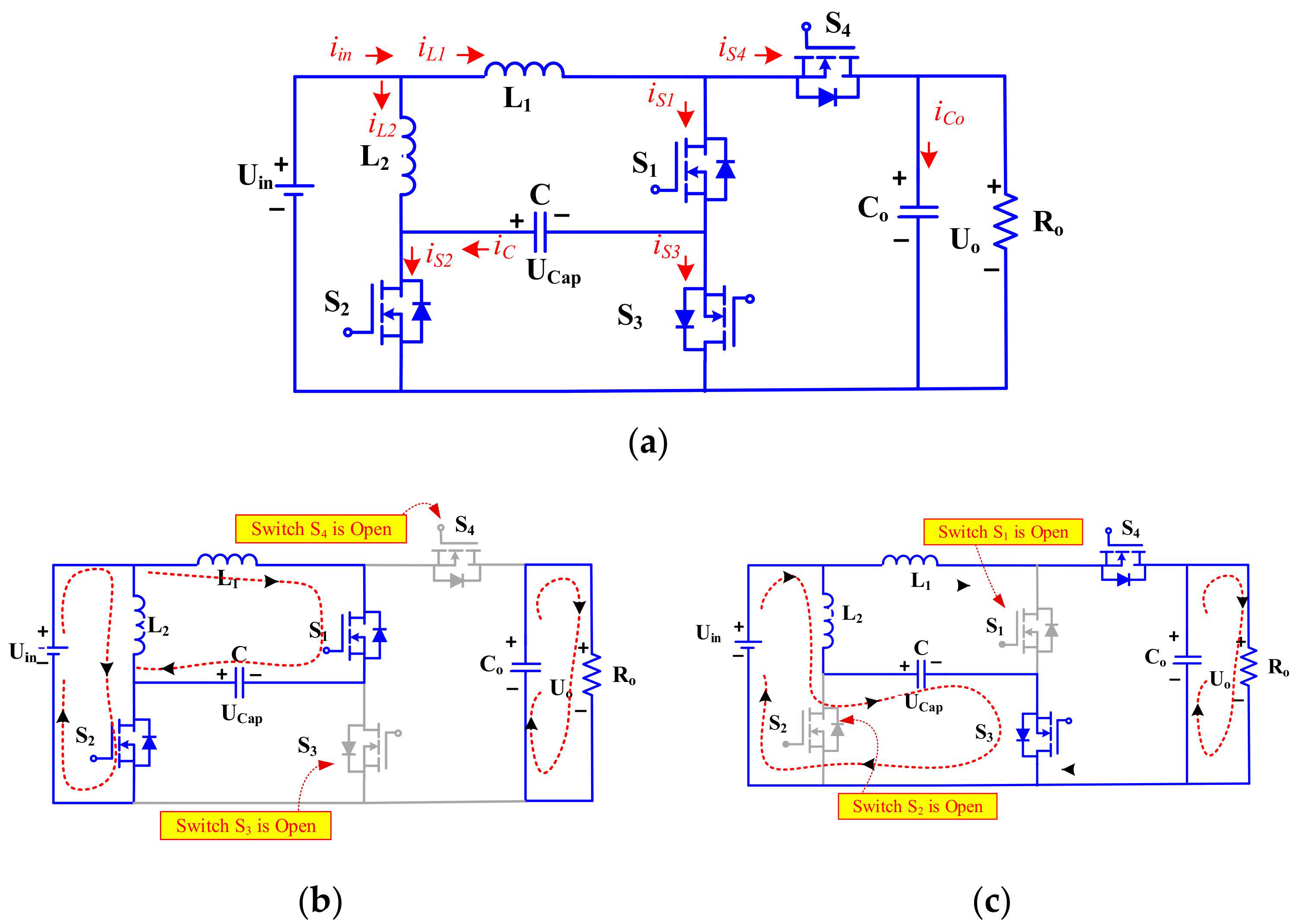
23], the circuit for the bidirectional converter is shown in
Figure 1, which contains four switches along with an inductor and wherein two capacitors are used to obtain the wide conversion range of voltage, but it has some constraints; during buck mode, the output voltage should have a maximum of half of the input voltage, while, during boost mode, the output voltage must be greater than twice the input voltage. In addition, due to the presence of one inductor in this circuit, its average value of the current is closer to the conventional converter. In [
24], an extensive voltage-gain can be realized in an H-bridge type converter short of a common ground which can be formed by associating in equivalent form of double power cells that are bidirectional in character. The deficit of [
24] is evaded in [
25] by using an asymmetric type H-bridge taking a common grounded form in which the pulse signals are by means of modulation indices along with the carrier waveforms. A combination of buck-boost nature of two-phase converter having an inter-leaved type along with a charge-pump on the high voltage-side and an unregulated type converter at the low voltage-end can be realized in [
26], which forms two phase switching control configuration. In [
27], a converter having phase shift of an isolated dual active configuration with a full bridge type is conferred in [
27], which is suitable for battery energy storage systems. A converter based on voltage-clamped along with a coupled-inductor chosen for the system had energy storage conferred in [
28], in order to obtain a wide gain by means of varying the inductor turns ratio. Various topologies of converter that are bidirectional studied to obtain a high gain as well as efficiency are reviewed in [
29]. Three sets of converters can be seen in [
30], among which the boost converter combined with any one of the Sepic/Cuk/Buck-Boost types to form the three structures and compared its feasibility. In [
31], to attain a high value of voltage-gain, the authors utilized a three winding style of a coupled inductor, though its design becomes complicated during structural implementation. In [
32], a high transformation ratio has been achieved with a three winding nature of a coupled inductor, which includes leakage inductance along with magnetizing inductance, which are complex to design owing to its dissimilar turn’s ratio. The configuration of conventional converter of boost/buck type is very simple as it involves less components and allows for the easiest way to control, but is restricted to obtain low voltage-gain value in both boost as well as buck operations. In addition, in the conventional converter, the inductor current is equal to the input current, which is similar to the switch current. The various converters discussed in this literature have several restrictions to accomplish high gain as well as high efficiency.
A modified topology is proposed based on [
22], by introducing one additional switch, an inductor, and a capacitor with the converter circuit in [
22]. The components count in this proposed topology involves the same number of switches but with two inductors and a capacitor is utilized when compared to the converter in [
23]. The proposed work effectively developed a converter with a high conversion ratio and improved efficiency. The values of the two inductors are different, hence its currents also differ, which results in the average of its current being less than the converter in [
23]. In order to enhance the voltage gain, the modified topology forms two boost converters. In addition, the input current is separated among the inductors, which results in reducing its size. It has been demonstrated that the proposed topology resulted in an enhanced voltage gain in comparison with the converters in [
22,
23]. During the step-down operation of the proposed work, among the four switches, one of the switches carries the sum of the two inductor currents which is very high when compared to the other switch currents. By using synchronous rectification instead of diode rectification in this particular switch, switching losses is greatly reduced, which results in an increase in efficiency. In addition, the proposed work should operate for a wide range of duty ratios under both boost and buck operations when compared to the converter [
22,
23]. This proposed bidirectional type of DC–DC converter during step-down operation is suitable for low output voltage with a high current of battery charging applications.
The following section involves the analysis of the proposed method; its operating principle and steady-state analysis are discussed in
Section 2. Comparisons and discussions of the proposed type with the conventional converters are described in
Section 3.
Section 4 presents the simulation study of the proposed topology. Experimental verifications are discussed in
Section 5, while
Section 6 presents the conclusions along with the summarization of outcomes.
3. Comparison and Discussion
A conventional cascaded type bidirectional buck/boost converter shown in
Figure 9 is compared with the proposed converter.
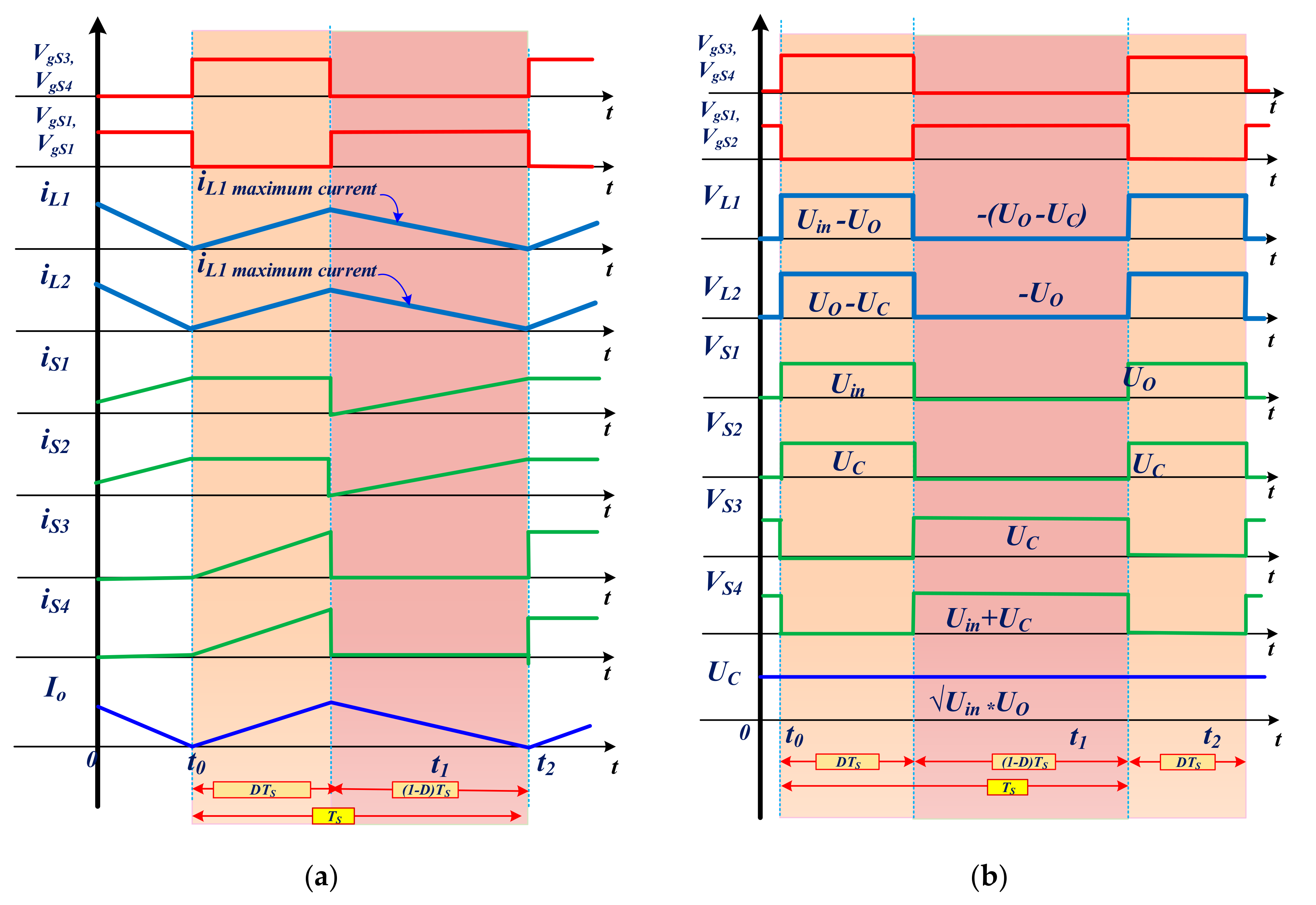
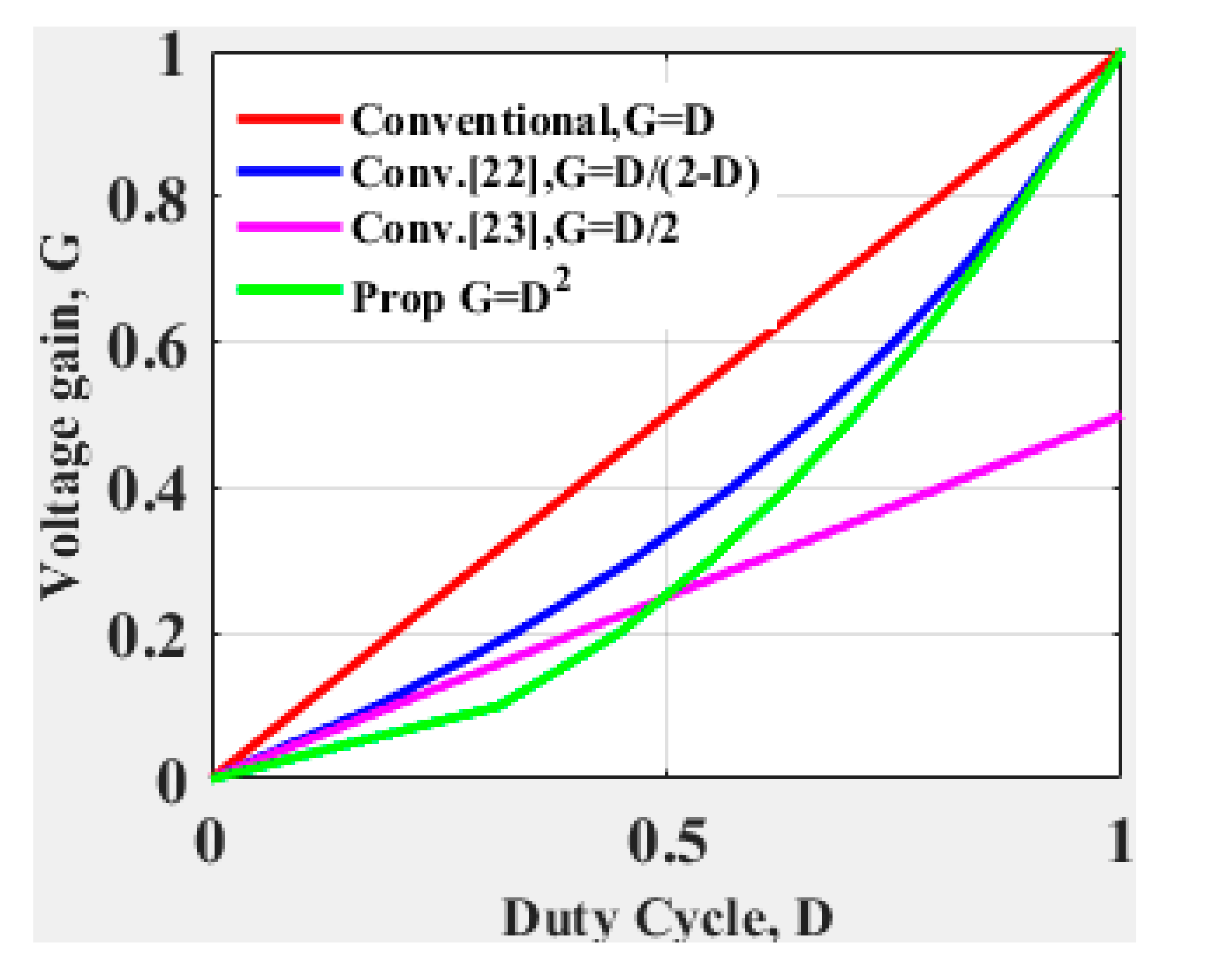
The voltage gains for boost operation and buck operation of the converter in the proposed topology are as follows:
The cascaded type and the proposed type are similar to the voltage gain, but the presented work has certain benefits that highlight additional applications. From the cascaded type, the inductor currents along with their ripples are expressed as
As voltage gain of cascaded type and the proposed converter are similar, the inductor currents as well as their ripples in the presented converter are seen to be
where U
in, U
0, and P
0 are the input-voltage side, output-voltage side, and the output power based on the boost or buck converters, respectively.
From the above Equations of cascaded type as well as the proposed one, it is identified that, in Equations (38) and (36), the inductor current IL1 of the presented type is similar to the inductor current IL2 of the cascaded type, whereas from Equations (40)–(34), it is shown that the inductor current IL2 of the presented converter is less significant than the inductor current IL1 of the cascaded type. This results in the size of inductor L2 of the presented type being smaller than the inductor L1 of the cascaded type.
The voltage and current stresses of the switching devices in the presented converter are:
The converter in [
23] is shown in
Figure 1. During step-up mode, the input current is equal to the inductor current and is shared among the switches based on the modes of operations. While during step-down operation, the input current is shared among the switches based on the modes of operations, but the inductor current is equal to the load current. Here, the average values of the switch currents are less than the conventional converter.
The proposed topology is shown in
Figure 2, and it contains two different values of inductors, resulting in the average values of the switch currents being different. From Equations (45)– (47), the current stresses of each switch can be determined, in that the currents in the switches S
1 and S
4 are the same and equivalent to the inductor current, I
L1, while the current in the switch S
3 has the value equal to the inductor current, I
L2. These values are lesser than the average values of the switch currents in the converter of [
23]. However, the current in switch S
2 is the addition of the two inductor currents, which has an edge over [
23] when this switch is used as a synchronous rectifier during step-down operation. In addition, in the proposed structure, the four switch current values during boost and buck modes are similar. For the step-up operation, for a gain value of less than or equal to 5, the converter [
23] is suitable, but, for the higher gain values, its duty cycle becomes large, which is shown in
Figure 5. For a large gain value of the converter [
23], the duty cycle becomes high, hence the switching losses increase, which reduces its efficiency. In addition, for the step-down operation, the converter [
23] has restrictions of the maximum gain value of 0.5, but the proposed converter results in less gain compared to the converter [
23], which is shown in
Figure 8. Hence, the proposed type is superior for large gains during step-up operation and lower gain during the step-down operation when compared to [
23].
Based on [
33], in bidirectional converters, synchronous rectification plays a key role in order to achieve higher efficiency. During step-down operation, the switches S
3 and S
4 are as power switches, whereas S
1 and S
2 are synchronous rectifiers. Hence, synchronous rectification can be utilized for switch S
2 of the proposed converter during step-down mode because its current value is very high, in which the efficiency has been increased when compared with the converter in [
23]. At the same time, the converter in [
23] has the constraints of maximum gain of 0.5 for the duty cycle of one during step-down mode; that is, gain value is always half of the duty cycle.
The cascaded type converter is shown in
Figure 9, and its switch stresses in total are seen to be
Voltage and current stresses in the switches are U
j and I
j, respectively. S represents total active switch stresses and is given by
Similarly, the overall active switch stresses in cascaded type is given by
From expressions (10)–(12) for the inductor currents, the input power as well as output power during the step-up operation is written as
The powers accompanying under step-down operation are
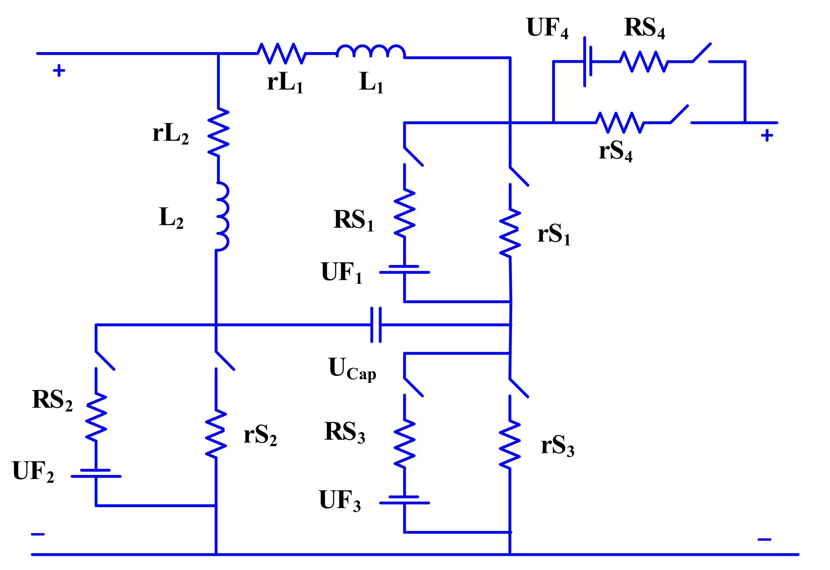
The equivalent circuit of the proposed topology is shown in
Figure 10, which include the conduction losses of the components and offset voltages of diodes while capacitors are assumed to be ideal. The current flow path under CCM for each mode of the equivalent circuit is identical to the main circuit.
From the equivalent circuit diagram of proposed work, the inductor voltages under the status of step-up can be seen as
Similarly, the inductor voltages during the status of step-down can be seen as
where r
s is the drain-source resistance of the power switches, and R
s is the on-state resistance of the body diode of the switches.
Based on [
34], the proposed topology under step-up mode, the switching losses on the MOSFET switches can be written as follows:
Ferrite core types of inductors are used in which the measurement of core loss [
34] needs some arrangements for evaluating flux density comprise the estimation of hysteresis B-H curve or loop areas. From the data sheet of the ferrite core, the curves related to B-H loop support to estimate the inductor core loss. Such B-H curve points to power loss density in terms of mW/cm
3, which is a function of switching frequency, fsw, and a peak-to-peak flux density ∆B. The voltage across the inductor based on Faraday’s law can be expressed as
Hence, in an inductor of a DC–DC converter, the peak flux density ∆B can be attained as
where U
L is the inductor voltage during the power switch is ON (DT
S), N is the number of turns around the inductor core, and A
C is the core area of an inductor. Therefore, the core loss can be attained as
where ℓ
mag is the magnetic path length of the core. By using (63), for the inductors L
1 and L
2, its core loss density (∆B) can be written as
Applying the voltage-second (V-S) balance technique on the inductor voltages, by using Equations (56) and (57), and the inductor current Equations in (11) and (12), and also considering the various losses using Equations (63) and (64), the efficiency of the presented work under step-up operation can be derived as
where
Similarly, from [
34], the proposed topology under step-down mode, the switching losses on the MOSFET switches can be expressed as follows:
In addition, the core-loss density (∆B) under step-down mode for the inductors L
1 and L
2 can be obtained as
For the same specifications of input and output voltages (UH, UL), switching frequency (fsw) and output power (P0) of the presented converter, the core loss on the inductors under step-up and step-down modes are identical.
Applying voltage-second (V-S) balance technique on the inductor voltages, by using Equations (58) and (59), and the inductor current Equations in (27) and (28), and also considering the various losses using Equations (63) and (64), the efficiency of the presented work under step-down operation can be derived as
where
Consider a voltage value of 180 V as output for the step-up and input for the step-down operations. Three cases of different gain values are to be discussed for both directions of the bidirectional DC–DC converters. In general, Gain step-down = 1/ Gain step-up
Case A: 12 V to 180 V; (Gain step-up = 15)
Case B: 18 V to 180 V; (Gain step-up = 10)
Case C: 24 V to 180 V; (Gain step-up = 7.5)
Comparisons of the efficiencies under different power ratings and gain values for the proposed topology with the converter in [
23] and the cascaded type under step-up and step-down operations have been carried out for three different cases. For all of the above-mentioned three cases, the parameters of converters are considered while comparisons of the proposed work with the cascaded type are as follows:
rS2 = rS3 = 55 mΩ, rS1 = rS4 = 0.27 Ω; RS1 = RS2 = RS3 = RS4 = 0.1 Ω; L1 = 200 µH, L2 = 15 µH, rL1 = rL2 = 0.1 Ω; fSw = 30 kHz, where rS and Rs are the drain to source resistance of the power switches and ON-state resistances of their body diodes and all the forward voltage drops UF of the switches are equal to 1 Volt.
By considering these three cases of voltage levels mentioned above, under various power ratings, using Equations (67) and (72), the calculated efficiency versus power for the proposed circuit along with the cascaded type, and the converter in [
23], are shown in
Figure 11a for step-up operation and
Figure 11b for step-down operation. It is evident that the proposed converter with large duty cycles has higher efficiency under various power ratings particularly when compared with the cascaded type and also with the converter in [
23].
The voltage gain of the proposed type purely depends on the duty cycles, the efficiency with the different values of duty cycles for two different power ratings are shown in
Figure 12a for step-up operation and
Figure 12b for step-down operation.
4. Simulation Study
The operation of presented circuit and its performance calculation was obtained using the MATLAB/Simulink package software, and its relevant results were discussed. The parameters as well as specifications relevant to the simulation work are as follows: for the step-up operation, the input voltage (U
in) of the converter = 12 V, and the output voltage (U
0) of the converter = 180 V, power associated in the converter = 200 W, maximum duty cycle for step-up mode, δ = 0.742 and switching frequency, f
sw = 30 kHz. The inductor values were L
1 = 200 µH and L
2 = 15 µH receptivity. The capacitors were C = C
0 = 220 μF.
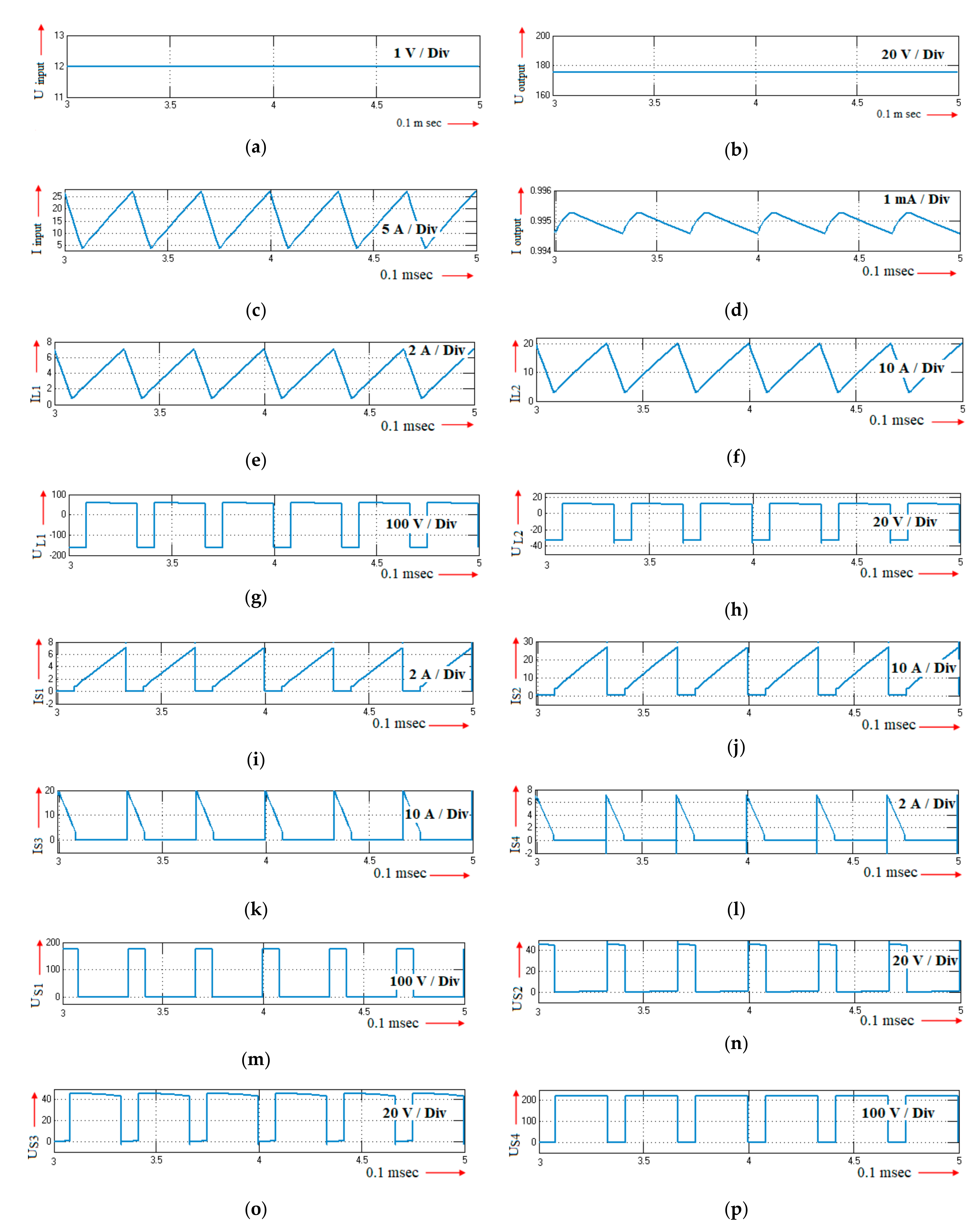
Figure 13 shows simulation results for the step-up operation of the proposed converter operating at switching frequency of 30 kHz and for a duty ratio of 74.2%, and the results perfectly match the theoretical values.
From
Figure 13a,b, when the duty ratio of the converter was kept at 0.742 for the applied voltage of 12 V, the converter provided a voltage of 176.8 V (14.733 times greater than the applied voltage) at the output terminals. During the operation of converter under CCM, the current in the inductor 1, I
L1 was saturated within the band range of 1 to 7.5 A, while the current in the inductor 2, I
L2 was saturated within the band range of 4 to 20 A and maintained continuously the input current of the converter shown in
Figure 13c.
Figure 13e,f show the inductor current waveforms, with I
L1 and I
L2 obtained from simulation. From these waveforms, it is identified that both the inductors L
1 and L
2 were uniformly charging and delivering the current continuously during conduction. From the simulation waveforms of the inductor currents, it can be inferred that the presented topology maintains the current in a continuous manner.
Figure 13d represents the output current waveform which has the value of approximately 0.995 A.
Figure 13g,h shows inductor voltages, U
L1 and U
L2, and
Figure 13m–p displays voltage across the power switches, U
S1 to U
S4, respectively. From these waveforms, it could be inferred that, during the operating period, the switches (MOSFET) followed their voltage in a maximum allowable range of 200 V and 500 V.
Figure 13i,l shows the switch current waveforms I
S1 to I
S4. From these waveforms, it is shown that the switch currents, I
S1 and I
S4, are equal to the inductor current I
L1, while I
S3 is equal to the inductor current I
L2, the switch current I
S2 is the sum of the two inductor currents, I
L1 and I
L2. From
Figure 13q, the capacitor voltage results in the square root of the product of the input and output voltages.
Figure 13r represents the waveform for the output capacitor voltage.
Similarly, for the step-down operation, the voltage input (U
in) of the converter = 180 V, and the voltage output (U
0) of the converter = 12 V, power associated in the converter = 200 W, maximum duty cycle for step-down mode, δ = 0.258 and operating at switching frequency f
sw = 30 kHz. The inductor values were L
1 = 200 µH and L
2 = 15 µH receptivity. The capacitors were C = C
0 = 220 μF.
Figure 14 shows simulation results for the step-down operation of the proposed converter operating at a switching frequency of 30 kHz and duty ratio of 25.8%; the results verified the theoretical values. From
Figure 14a,b, when the duty ratio of the converter was kept at 0.258 for the applied voltage of 180 V, the converter provided a voltage of 11.88 V (0.066 times smaller than the applied voltage) at the output terminals. During the operation of converter under CCM, the current in the inductor 1, I
L1 was saturated within the band range of 1 to 7.5 A, while the current in the inductor 2, I
L2 was saturated within the band range of 4 to 20 A and maintained continuously the input current of the converter shown in
Figure 14c.
Figure 14e,f shows the inductor current waveforms, and I
L1 and I
L2 were obtained from simulation. From these waveforms, it is identified that both of the inductors L
1 and L
2 were uniformly charging for the mentioned duty period of 25.8% and delivering the current continuously during conduction. From the simulation waveforms of the inductor currents, it can be inferred that the presented topology maintains the current in continuous manner.
Figure 14d represents the output current waveform which has the value of approximately 16.1 A.
Figure 14g,h shows inductor voltages, U
L1 and U
L2, and
Figure 14m–p displays voltage across the power switches, U
S1 to U
S4 respectively. From these waveforms, it could be inferred that, during the operating period, the switches (MOSFET) had their voltage in a maximum allowable range of 200 V and 500 V.
Figure 14i–l shows the switch current waveforms I
S1 to I
S4; from these waveforms, it is shown that the switch currents, I
S1 and I
S4, are equal to the inductor current I
L1, while I
S3 is equal to the inductor current I
L2, and the switch current I
S2 is the sum of the two inductor currents, I
L1 and I
L2. From
Figure 14q, the capacitor voltage results in the square root of the product of the input and output voltages.
Figure 14r represents the waveform for the output capacitor voltage.
From
Figure 13m–p and
Figure 14m–p, the voltage stress U
S1 is nearly equal to 176.8 V across the switch S
1. In addition, voltage stresses U
S2 and U
S3 are nearly equal to 46.4 V across the switches S
2 and S
3. Then, the voltage stress U
S4 is nearly equal to 223.2 V across the switch S
4. Similarly, the voltages across the inductors for the various statuses under boost and buck operations are equal. Considering the simulations waveforms of current shown in
Figure 13g–j and in
Figure 14g–j, from the switch currents, i
s1 and i
s4, it can be identified that its stresses are same, its values are i
s1peak = i
s4peak = 4.3 A. In addition, from the waveforms of the switch currents i
s2 and i
s3, the current stresses are the values as i
s2peak = 16.28 A and i
s3peak = 11.94 A, respectively.
From the above simulation waveforms of the proposed work, the simulation results agree well with the theoretical values.
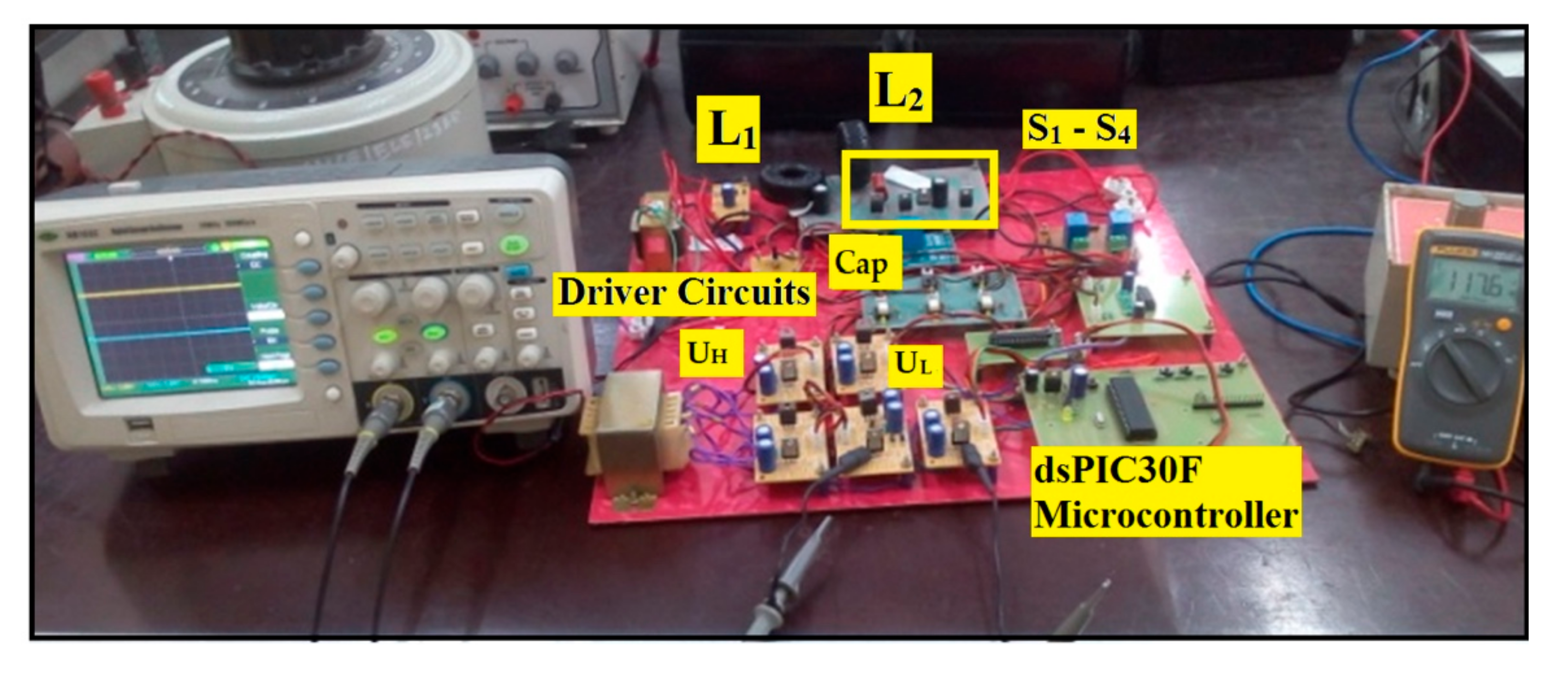
5. Experimental Verifications
In order to validate the theoretical and simulation results, a 12 V/180 V, 200 Watts prototype model of the presented bidirectional converter has been designed, implemented as well as examined to validate its performance. The experimental set-up for the presented topology is illustrated in
Figure 15. The hardware model of the presented topology is implemented by using a dsPIC30F microcontroller operating at a clock frequency of 30 MHz, which corresponds to a time period of 33.33 ns. Switching frequency of the converter is selected as 30 KHz, and appropriate numbers of clock signals are generated for each time interval. IRFP460 and IRFP260 were used for MOSFET switches S
1, S
4 and for S
2, S
3.
For the prototype model of the converter, the experimental relevant parameters are given in
Table 1.
The maximum rate of energy stored in capacitor in step-down operation for every cycle T
s is
From (29) and (30), the minimum value of the output capacitance (C
0) under step-down mode is derived as
The peak voltage across the equivalent series resistance (ESR) of the output capacitor under step-down mode can be expressed as
While considering a certain ripple value, the capacitor C
0 size is calculated by (72). After knowing the ESR of the selected capacitor, the voltage–ripple is determined as ∆U
C0ESR + ∆U
C0, to be patterned to be smaller than the desired value of the voltage–ripple. Hence, the sizes of capacitors C
0 in the step-up mode and Cap are expressed as
As per the capacitor value C
0 for the step-down mode described, then, after choosing the capacitor Cap and C
0 for the step-up mode, its ESR values can be found. Hence, the voltage drop and its ESR values for Cap and C
0 under step-up operation can be derived as
Conferring to the above-mentioned Equations, to provide the capacitor voltage ripple to be less than 5%, its values are chosen to be large and adequate.
During the step-up operation of the proposed topology, consider the input voltage side; that is, the low voltage and the output load resistor are U
in = 12 V and R
0 = 162 Ω, respectively. In order to drive the proposed topology under CCM, the inductance values of L
1 and L
2 for the duty cycle, D = 0.742, switching frequency, f
sw = 30 kHz and the output resistor, R
0 = 162 Ω can be obtained as L
1 ≥ 168 µH and L
2 ≥ 12 µH. Hence, the values of the two inductors are chosen as 200 µH and 15 µH, respectively. These inductor values are common for both boost and buck operations. The experimental results illustrated in
Figure 16 are for step-up operation. According to Equation (7), for the given parameters in
Table 1, the output voltage is attained as U
0 = 180 V. From
Figure 16d, the output voltage is nearly equal to 176.6 V, similar to the value obtained from the theoretical analysis.
Considering the waveforms from
Figure 16b, it can be shown that, across each of the switches, its voltage stress is similar to the simulated values. In addition, for the inductors, its voltages are determined by considering Equations (1)–(4), for an inductor1, U
L1 is equal to 58 V for mode I and −165.6 V for mode II. Similarly, for inductor 2, U
L2 is equal to 12 V for mode I and −34.1 V for mode II. From
Figure 16a, it can be observed that the voltages across the inductors are similar to the theoretical values.
For the step-up operation, switches S
1 and S
2 act as control switches and S
3 and S
4 are synchronous rectifiers.
Figure 16c shows the switch current waveforms for S
1 to S
4, which are similar to the simulation values. In addition, for the inductor currents, it can be seen that the values of L
1 and L
2 are found as 4.34 A and 11.94 A shown in
Figure 16a, which shows that its values are almost equal to the simulated values. In addition, for the power circuit for step-up operation shown in
Figure 3a, the input current is divided by the two inductors, and its value is also verified by
Figure 16a. In addition, the output current based on the load value of 162 Ω can be determined as I
0 = U
0/R
0, which is equal to 1.11 A, can be obtained as very close to the value of 1.08 A shown in
Figure 16d. Thus, the theoretical results and the prototype results are validated for the step-up operation.
In the step-down operation, consider the input voltage side, where the high voltage and the output load resistor for a 200 watts output power are kept as U
in = 180 Vand R
0 = 0.72 Ω for a duty cycle, D = 0.258, respectively. For the step-down operation, its experimental waveforms are illustrated in
Figure 17. The output voltage based on the parameters in step-down operation is obtained from the simulation results as 11.88 V and experimentally as 11.86 V, shown in
Figure 17 d. The voltage stress across each switch in buck and boost operations has similar values, shown in
Figure 16b and
Figure 17b. In addition, the voltage across the inductor 1, U
L1 is equal to 168.4 V for mode I and −57.96 V for mode II. Then, for an inductor L
2, U
L2 is equal to 34.24 V for mode I and −11.86 V for mode II, which are vice versa as per the step-up mode. From
Figure 17d, it can be observed that the voltages across the inductors are similar to the simulation and theoretical values.
During the step-down operation, switches S
3 and S
4 perform as switches and likewise S
1 and S
2 are synchronous rectifiers. By considering the switch current waveforms of is
1 and is
4 shown in
Figure 14g–j, the current stresses for the switches S
1 and S
4 are equal in magnitude, and its values are equal, which are as i
s1peak = i
s4peak = 4.32 A. In addition, the current stresses for the switches S
2 and S
3 are its values approximately are as i
s2peak = 16.26 A and i
s3peak = 11.94 A.
Figure 17c shows the current waveforms for all the switches, which are nearly equal to the simulation waveforms and also its values are almost identical. In addition, for the inductor currents, by considering Equations (34) and (36) and from the simulation waveforms, it can be seen that the values of L
1 and L
2 are found as 4.34 A and 11.94 A, which show that its values are almost equal as shown in
Figure 17a. In addition, for the power circuit for step-down operation shown in
Figure 6a, the average value of the output current in the step-down operation is the addition of the two inductor currents. Based on the 200 watts output power rating, its load resistance is 0.72 Ω, and the output current can be determined as I
0 = U
0/R
0, equal to 16.64 A, which can be obtained very close to the value as 16.56 A shown in
Figure 17d. For the step-down operation, the theoretical value that has been obtained as depicted in
Figure 7 is verified from the results experimentally as shown in
Figure 17.
When comparing the switch currents of the proposed type, its average values of the switch currents in S1, S3, S4 are lower, while the current in the switch S2 is high; this has as an advantage during step-down operation of the proposed type, due to the switch S2 being used as a synchronous rectifier. When the drain to source resistance of the power switch S2 is less than the on-state resistance of the body diode, synchronous rectification can be applied, where the efficiency plays a vital role. At the same time, if the synchronous rectification is applied to the switches S1, S3, S4, its efficiency is sufficiently less because of its drain to source resistance and also its less current values. Thus, the step-down operation has an advantage in this proposed type because of synchronous rectification for the switch S2 to attain higher value of efficiency under the power rating of 200 W.
Experimental results from the prototype model under the operations in step-up and step-down are depicted in
Figure 16;
Figure 17. The inductor currents I
L1 and I
L2 are about 4.34 A and 11.94 A verified, respectively, in both modes of operation under step-up and step-down. It is evident that the duty cycle of the proposed type indeed contributed to the increase in efficiency.
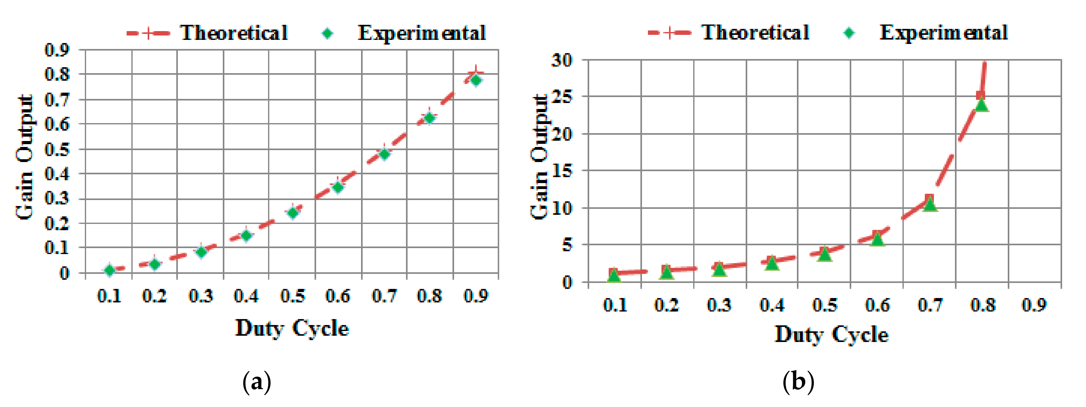
In order to validate the gain values with different duty cycles in terms of theoretical and experimental values of the proposed topology under continuous conduction mode, a curve between voltage gain output with duty cycle in the range of 0.05 to 0.75 were drawn for both step-up and step-down operations which are predicted in
Figure 18a,b. From these curves, it can be identified that the experimental gain values are very close to the theoretical values.
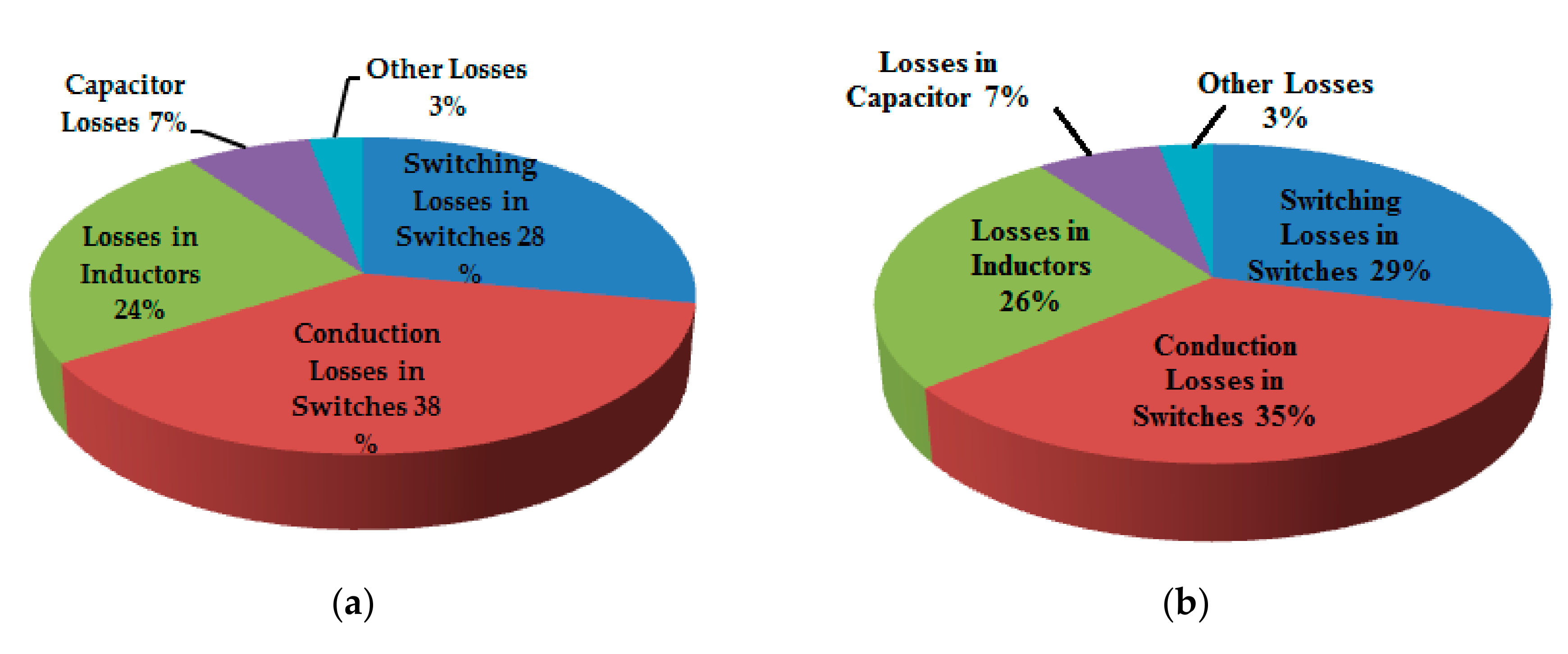
Figure 19a,b shows the loss distribution of the experimented converter under rated load condition for the duty cycle of D = 0.742 under step-up and D = 0.258 under step-down operations. The switching losses as well as the conduction losses across the power switches are about 65% of the total losses. The total losses of the experimented converter under step-up mode are nearly equal to the value of 16.4 watts, among which 10.82 watts are due to the switching and conduction losses in the power switches, 3.94 watts are due to the losses in the inductors, and the remaining losses are due to capacitors and the other losses, which are shown in
Figure 19a. Due to the synchronous rectification, the total losses in the step-down mode are about 12.38 watts. Out of these losses, 7.92 watts are due to the power switches and the remaining losses are due to the inductors, capacitors, and other losses which are predicted in
Figure 19b.
By considering with and without synchronous rectification method in the proposed work, the comparisons of the calculated and measured efficiencies under various different power ratings for both step-up and step-down operations are represented in
Figure 20.
The efficiency value under step-up operation is measured as 94.1% when compared to its calculated value of 97.1% because of the switch S2 working as the control switch, and its current stress is the summation of the two inductor currents, which is high; there are more switching losses, and the efficiency becomes 94.1%. During step-down operation, it is measured as 95.1% when compared to its calculated value of 95.5% because switch S2 is working as a synchronous rectifier; hence, the switching losses becomes lower and improves the efficiency during step-down operation. Hence, synchronous rectification can be used in the step-down operation particularly for the battery charging applications of low output voltage with high current.
From this, it should be clear that the proposed work not only attained a larger gain value, but its efficiency is also better when compared to the other bidirectional types under consideration. Some of the converters discussed achieve high efficiency, but it has a low amount of gain, while its gain is increased, which degrades its efficiency. Therefore, its input powers for the proposed work under both the operations of step-up and step-down are about 200 W. In the operation of step-down, the output power is measured from the current and voltage values as 184 W, whose efficiency is 94.1% for step-up and 95.1% for step-down operations. Thus, the proposed type gives a better efficiency with large voltage-gain value particularly when compared to the converters discussed.
Performance comparisons of various existing bidirectional type of converters discussed along with the proposed topology based on rated load condition are shown in
Table 2.
From
Table 2, when compared to various existing converters particularly in [
22,
28], coupled inductors are used, which are difficult to design by considering the effect of coefficient of coupling factor. In addition, for the existing converters in [
23,
24,
25], a single inductor is used which is suitable for the conversion of specified gain values. Beyond that, the size of the inductor becomes bulky. These limitations are overcome in the proposed converter by introducing two different values of inductors; hence, its current values differ, which becomes an advantage to enhance the voltage gain during step-up operation by means of forming two boost converters in the proposed topology and also resulting in high efficiency during step-down operation by using synchronous rectification. The existing converters mentioned in
Table 2 are suitable for providing high efficiency during a smaller range of gain values only. If the gain values of the existing converter increase, its efficiencies degrade. From these experimental results of the proposed converter, it is well suited for large gain values with high efficiency. The discussion and analysis, the experimental results, and the comparisons confirm the benefits and functionality of the proposed converter.


